 | –≠–ª–µ–∫—Ç—Ä–æ–Ω–Ω—ã–π –∫–æ–º–ø–æ–Ω–µ–Ω—Ç: CDB5321 | –°–∫–∞—á–∞—Ç—å:  PDF PDF  ZIP ZIP |
15
Copyright
©
Cirrus Logic, Inc. 1998
(All Rights Reserved)
Cirrus Logic, Inc.
Crystal Semiconductor Products Division
P.O. Box 17847, Austin, Texas 78760
(512) 445 7222 FAX: (512) 445 7581
http://www.crystal.com
CDB5321
Evaluation Board for CS5321 and CS5322
Features
l
DIP switch control of all CS5322 logic pins
l
Header control of all CS5322 logic pins
l
Supports manual operation of RESET and
SYNC
Description
The CDB5321 is an evaluation board that allows labora-
tory characterization of the CS5321/CS5322 A/D
converter chip-set. The chip-set supports seven different
selectable word rates: 4 kHz, 2 kHz, 1 kHz, 500 Hz
250 Hz, 125 Hz and 62.5 Hz. Input to the board is 9 volts
peak-to-peak. Output is via header connections to the
CS5322 serial interface.
ORDERING INFORMATION
CDB5321
Evaluation Board
I
Reference
Circuitry
CS5321
Headers
+5V
+5V Digital
+5V
DGND
-5V Analog
AGND
-15V
+15V
+5V Analog
AIN
SYNC
+5V
Regulator
-5V
Regulator
VREF+
AIN+
AINR
MSYNC
MCLK
MDATA
MFLG
MSYNC
MCLK
MDATA
MFLG
CS5322
DIP Switch
Selections
2.048 MHz
Oscillator/
Divider
CLKIN
8
+5V
RESET
9
DIP Switch
Selections
MAR `95
DS88DB2
IN
OUT
GND
78L05
+15 V
+15V
47
µ
F
D2
1N6276
0.1
µ
F
+
0.1
µ
F
0.1
µ
F
IN
OUT
GND
79L05
-15 V
-15V
47
µ
F
1N6276
0.1
µ
F
+
0.1
µ
F
- 5VA
47
µ
F
+
0.1
µ
F
+5V
+5V
DGND
6.8V
D1
C3
C4
C11
C12
C13
2
IN
6
5
OUT
TRIM
10K
R16
+5VA
+5VA
C14
VREF
(4.5 V)
4
D3
C16
C17
GND
C18
- 5VA
To
Figure 2
LT1019
4.5V
P6KE
3
U6
1
2
R2
2 K
10
µ
F
C7
+
U8
OPTIONAL
2
1
3
U9
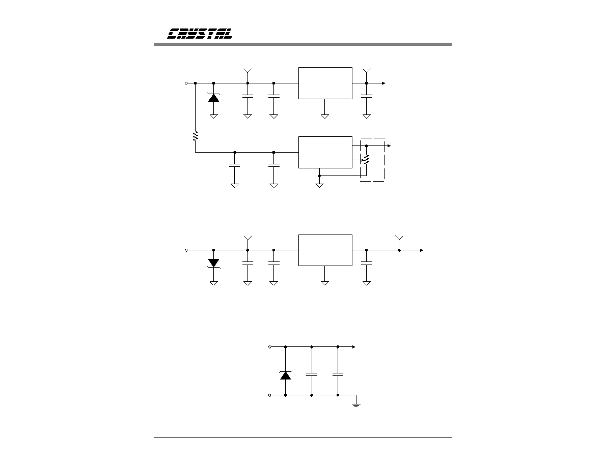
Figure 1. Power Supplies
CDB5321
16
DS88DB2
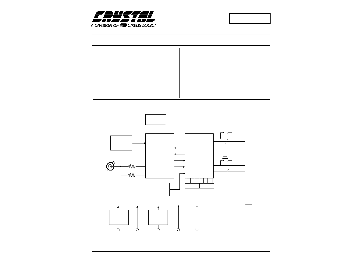
OVERVIEW
The CDB5321 evaluation board requires three
separate power supplies for proper operation.
Figure 1 illustrates the power supply connec-
tions. The required power supply input voltages
consist of +5V, +15V, and -15V. The CS5322
filter and logic support devices on the board op-
erate from the +5V supply. The +15V and
-15V inputs are regulated down to provide +5V
and -5V supplies necessary for the CS5321
modulator. Figure 1 also illustrates the LT1019
4.5V reference used with the CS5321 modulator.
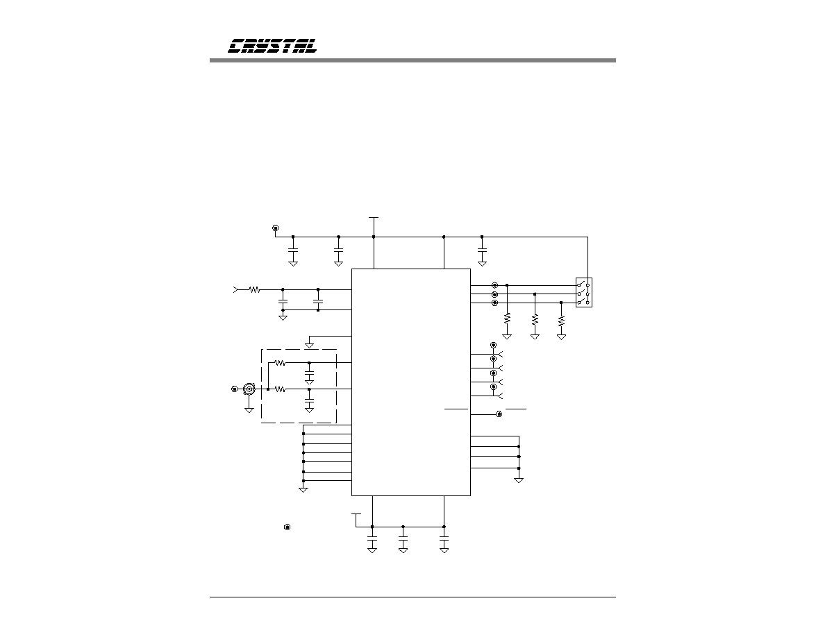
Figure 2 illustrates the CS5321 modulator cir-
cuitry, including the analog BNC input for the
test signal source. Most often switch selections
o n S 5 a r e s e t to HB R= 1 , LPW R= 0 , a nd
V1+
VREF+
VREF-
AIN-
AIN+
AINR
AGND1
AGND2
AGND3
AGND4
AGND5
AGND6
AGND7
V2+
OFST
LPWR
HBR
MCLK
MSYNC
MDATA
MFLG
DGND1
DGND2
DGND3
DGND4
V2-
V1-
2
5
6
8
9
10
3
1
4
7
11
12
13
14
22
28
27
26
20
25
18
17
24
23
19
16
15
21
U2
CS5321
C50
0.1
µ
F
C20
68
µ
F
R6
200
MDATA
MCLK
MSYNC
MDATA
MDATA
MFLG
VREF
-5 VA
C29
0.1
µ
F
C40
0.1
µ
F
TANT
AIN
R1
R5
402
C6
0.1
µ
F
NPO
402
C15
0.1
µ
F
NPO
R7
100k
R8
R9
100k
100k
+5 VA
C22
0.1
µ
F
C27
0.1
µ
F
C26
TANT
10
µ
F
TEST POINT
+
From
Figure 1.
C19
10
µ
F
+
To
Figure 4.
OFST
LPWR
HBR
See CS5321 Datasheet
S5
Figure 2. CS5321 Modulator Input Circuitry.
CDB5321
DS88DB2
17

OFST=1. Figure 3 illustrates the 2.048 MHz os-
cillator and dual D flip flop clock divider. Note
that both the oscillator and the divider are sepa-
rately decoupled from the +5V supply to reduce
clock jitter which can be introduced from noisy
supplies. Jumper J4 should be set in the CLK/2
position to source 1.024 MHz to the CS5322
chip for normal operation. If operation from
512 kHz clock is desired, the J4 jumper should
be changed to the CLK/4 position. The board
can be tested at 512 kHz without modification.
The digital interface pins to the CS5322 filter
chip are all available on the header connectors
J1, J2, and J3 as shown in Figures 4, 5, and 6.
Note that one row of pins on each of the headers
is ground. It is advised that any connections
made to control lines be done with twisted pair
ribbon cable; with each twisted pair containing
one signal and one ground connection. This
minimizes radiated noise.
CAUTION!
Caution is advised when interfacing the evalu-
ation board to any circuitry powered from
another source. For example, when interfacing
to a computer I/O card be sure that the evalu-
ation board and the computer are both powered
up before connecting to the evaluation board
headers. Always disconnect header connections
when powering down the board but not the com-
puter. Failure to follow this advice may cause
damage to either the computer I/O or to the
CS5322, because the computer outputs try to
power the CDB5321 board.
Q
CLK
Q
0.1
10
OSC
14 pin
10
+ 10
µ
F
7
74HC74
8
+5V
+5V
R3
C1
C2
R25
C33
2.048 MHz
14
U7
2
3
14
1
S
D
R
4
5
6
Q
CLK
Q
S
D
R
CLK/4 (512 kHz)
CLK/2 (1.024 MHz)
CLK (2.048 MHz)*
CLKIN (To Figure 4)
J4
10
9
8
13
11
12
U5A
U5B
*2.048 MHz
exceeds the
specified clock
frequency for
the CS5321
0.1
µ
F
Figure 3. Oscillator / Divider
CDB5321
18
DS88DB2
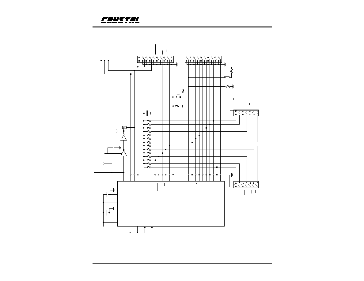
Figure 4. CS5322 Filter Interface
+5V
3
22
25
27
28
1
23
19
18
17
16
15
14
13
12
11
4
2
0.1
TP
100 k
RESET
5 k
DRDY
ORCAL
DECA
DECB
DECC
USEOR
PWDN
CSEL
TDATA
RST
SYNC
H/S
SID
RSEL
CS
ERROR
SCLK
SOD
26
24
+5V
47k
SIPS
+5V
R/W
0.1
µ
F
CLKIN
(From Figure 3)
SYNC
5K
+5VD
J3
J1
SID
RSEL
CS
ERR
R/W
ORCAL
USEOR
DECA
DECB
DECC
PWDN
CSEL
TDATA
H/S
DRDY
SCLK
SOD
To
Figure
5,6
4
3
1
2
U3A
U3B
C34
JP13
SW3
SW4
SCLK
100 k
R13
R12
R14
R11
0.1
µ
F
VD1+ DGND VD2+ DGND
CLKIN
DRDY
8
9
21
20
0.1
µ
F
MSYNC
MCLK
MDATA
MFLG
5
7
10
6
CS5322
ORCAL
DECA
DECB
DECC
USEOR
PWDN
CSEL
TDATA
RESET
SYNC
H/S
SID
RSEL
CS
ERROR
SCLK
SOD
+5V
R/W
To
Figure
2
C9
C8
CLKIN
U1
CDB5321
DS
88DB2
19