| –≠–Ľ–Ķ–ļ—ā—Ä–ĺ–Ĺ–Ĺ—č–Ļ –ļ–ĺ–ľ–Ņ–ĺ–Ĺ–Ķ–Ĺ—ā: CDB5333 | –°–ļ–į—á–į—ā—Ć:  PDF PDF  ZIP ZIP |
Advance Product Information
This document contains information for a new product.
Cirrus Logic reserves the right to modify this product without notice.
1
Copyright
©
Cirrus Logic, Inc. 2000
(All Rights Reserved)
P.O. Box 17847, Austin, Texas 78760
(512) 445 7222 FAX: (512) 445 7581
http://www.cirrus.com
Features
l
24-bit conversion
l
Supports 96 kHz sample rates
l
98 dB dynamic range at 3 V supply
l
-88 dBFS THD+N
l
1.8 to 3.3 volt supply
l
16-Pin TSSOP package
l
Low power consumption
≠ 11 mW at 1.8 V
l
Internal high pass filter to remove DC offsets
l
Linear phase digital anti-alias filter
Description
The CS5333 is a highly integrated, 24-bit, 96 kHz audio
ADC providing stereo analog-to-digital converters using
delta-sigma conversion techniques. This device includes
line level inputs in a 16-pin TSSOP package.
The CS5333 is based on delta-sigma modulation allow-
ing infinite adjustment of the sample rate between 2 kHz
and 100 kHz simply by changing the master clock
frequency.
The CS5333 operates from a +1.8 V to +3.3 V supply.
These features are ideal for set-top boxes, A/V receiv-
ers, DVD-karaoke players or any system which requires
optimal performance in a minimum of space.
ORDERING INFORMATION
CS5333-KZ
-10 to 70į C
16-pin TSSOP
CDB5333
Evaluation Board
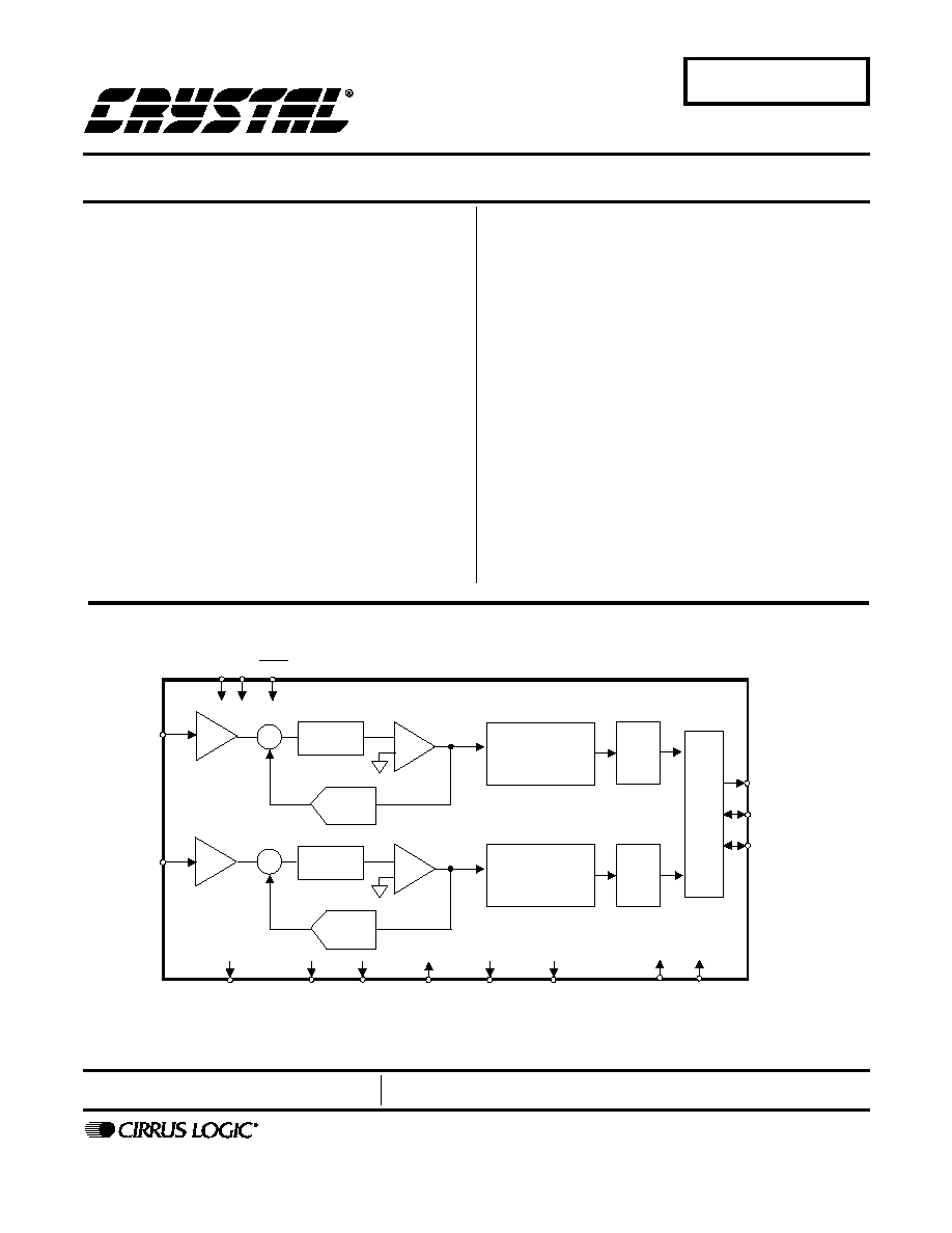
I I
M C L K
G N D
V Q
F I L T +
R E F _ G N D
S/H
S/H
C omparator
C omparator
DAC
DAC
LP Filter
LP Filter
+
-
+
-
+
-
+
-
AINR
AINL
Digital Decimation
Filter
Digital Decimation
Filter
HPF
HPF
Se
r
i
a
l
P
o
r
t
SDATA
LRCK
SCLK
V L
RS T
V A
D I V
D I F
TST
CS5333
24-Bit, 96 kHz Stereo A/D Converter
DEC `00
DS520PP1

CS5333
2
DS520PP1
TABLE OF CONTENTS
1. CHARACTERISTICS/SPECIFICATIONS ................................................................................. 4
ANALOG CHARACTERISTICS ................................................................................................ 4
ANALOG CHARACTERISTICS ................................................................................................ 5
POWER AND THERMAL CHARACTERISTICS....................................................................... 6
DIGITAL CHARACTERISTICS ................................................................................................. 7
ABSOLUTE MAXIMUM RATINGS ........................................................................................... 7
RECOMMENDED OPERATING CONDITIONS ....................................................................... 7
SWITCHING CHARACTERISTICS .......................................................................................... 8
2. TYPICAL CONNECTION DIAGRAM .................................................................................... 10
3. PIN DESCRIPTION ............................................................................................................... 11
4. APPLICATIONS ...................................................................................................................... 13
4.1 Grounding and Power Supply Decoupling ....................................................................... 13
4.2 Oversampling Modes ....................................................................................................... 13
4.3 Recommended Power-up Sequence ............................................................................... 13
4.4 Master/Slave Mode .......................................................................................................... 13
5. PARAMETER DEFINITIONS .................................................................................................. 17
6. REFERENCES ........................................................................................................................ 17
7. PACKAGE DIMENSIONS ....................................................................................................... 18
Contacting Cirrus Logic Support
For a complete listing of Direct Sales, Distributor, and Sales Representative contacts, visit the Cirrus Logic web site at:
http://www.cirrus.com/corporate/contacts/sales.cfm
Preliminary product information describes products which are in production, but for which full characterization data is not yet available. Advance product infor-
mation describes products which are in development and subject to development changes. Cirrus Logic, Inc. has made best efforts to ensure that the information
contained in this document is accurate and reliable. However, the information is subject to change without notice and is provided "AS IS" without warranty of
any kind (express or implied). Customers are advised to obtain the latest version of relevant information to verify, before placing orders, that information being
relied on is current and complete. All products are sold subject to the terms and conditions of sale supplied at the time of order acknowledgment, including those
pertaining to warranty, patent infringement, and limitation of liability. No responsibility is assumed by Cirrus Logic, Inc. for the use of this information, including
use of this information as the basis for manufacture or sale of any items, nor for infringements of patents or other rights of third parties. This document is the
property of Cirrus Logic, Inc. and by furnishing this information, Cirrus Logic, Inc. grants no license, express or implied under any patents, mask work rights,
copyrights, trademarks, trade secrets or other intellectual property rights of Cirrus Logic, Inc. Cirrus Logic, Inc., copyright owner of the information contained
herein, gives consent for copies to be made of the information only for use within your organization with respect to Cirrus Logic integrated circuits or other parts
of Cirrus Logic, Inc. The same consent is given for similar information contained on any Cirrus Logic website or disk. This consent does not extend to other
copying such as copying for general distribution, advertising or promotional purposes, or for creating any work for resale. The names of products of Cirrus Logic,
Inc. or other vendors and suppliers appearing in this document may be trademarks or service marks of their respective owners which may be registered in some
jurisdictions. A list of Cirrus Logic, Inc. trademarks and service marks can be found at
http://www.cirrus.com
.

CS5333
DS520PP1
3
LIST OF FIGURES
Figure 1. SCLK to LRCK and SDATA, Slave Mode ........................................................................ 9
Figure 2. SCLK to LRCK and SDATA, Master Mode ...................................................................... 9
Figure 3. Typical Connection Diagram.......................................................................................... 10
Figure 4. Base-Rate Stopband Rejection...................................................................................... 14
Figure 5. Base-Rate Transition Band............................................................................................ 14
Figure 6. Base-Rate Transition Band (Detail) ............................................................................... 14
Figure 7. Base-Rate Passband Ripple.......................................................................................... 14
Figure 8. High-Rate Stopband Rejection ...................................................................................... 14
Figure 9. High-Rate Transition Band............................................................................................. 14
Figure 10. High-Rate Transition Band (Detail) .............................................................................. 15
Figure 11. High-Rate Passband Ripple......................................................................................... 15
Figure 12. Line Input Test Circuit .................................................................................................. 15
Figure 13. CS5333 - Serial Audio Format 0 .................................................................................. 16
Figure 14. CS5333 - Serial Audio Format 1 .................................................................................. 16
LIST OF TABLES
Table 1. Common Clock Frequencies........................................................................................... 11
Table 2. Digital Interface Format - DIF.......................................................................................... 12
CS5333
4
DS520PP1
1. CHARACTERISTICS/SPECIFICATIONS
ANALOG CHARACTERISTICS
(T
A
= 25į C; GND = 0 V Logic "1" = VL = 1.8 V; Logic "0" =
GND = 0 V; MCLK = 12.288 MHz; Fs for Base-rate Mode = 48 kHz, SCLK = 3.072 MHz, Measurement Bandwidth
10 Hz to 20 kHz, unless otherwise specified; Fs for High-Rate Mode = 96 kHz, SCLK = 6.144 MHz, Measurement
Bandwidth 10 Hz to 20 kHz, unless otherwise specified.)
Notes: 1. Referenced to typical full-scale differential input voltage.
Parameter
Symbol
Base-rate Mode
High-rate Mode
Unit
Min
Typ
Max
Min
Typ
Max
Analog Input Characteristics for VA = 1.8 V
Dynamic Range
A-weighted
unweighted
TBD
TBD
91
88
-
-
TBD
TBD
94
91
-
-
dB
dB
Total Harmonic Distortion + Noise
(Note 1)
-1 dB
-20 dB
-60 dB
THD+N
-
-
-
-88
-68
-28
TBD
-
-
-
-
-
-88
-68
-31
TBD
-
-
dB
dB
dB
Analog Input Characteristics for VA = 3.0 V
Dynamic Range
A-weighted
unweighted
TBD
TBD
96
93
-
-
TBD
TBD
98
95
-
-
dB
dB
Total Harmonic Distortion + Noise
(Note 1)
-1 dB
-20 dB
-60 dB
THD+N
-
-
-
-88
-68
-33
TBD
-
-
-
-
-
-85
-65
-35
TBD
-
-
dB
dB
dB
Analog Input Characteristics for VA = 1.8 or 3.0 V
Interchannel Isolation
1 kHz
-
90
-
-
90
-
dB
Interchannel Gain Mismatch
-
0.1
-
-
0.1
-
dB
Offset Error
with High Pass Filter
-
-
0
-
-
0
LSB
Full Scale Input Voltage
TBD
VAų3.6
TBD
TBD
VAų3.6 TBD
Vrms
Voltage Common Mode
VAų2
VAų2
V
Gain Drift
-
100
-
-
100
-
ppm/įC
Input Resistance
10
-
-
10
-
-
k
Input Capacitance
-
-
15
-
-
15
pF
CS5333
DS520PP1
5
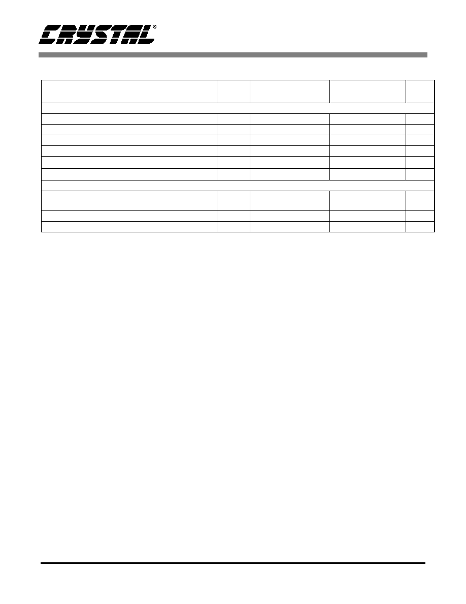
ANALOG CHARACTERISTICS
(Continued)
Notes: 2. Filter response is guaranteed by design.
3. Filter characteristics scale with output sample rate. For output sample rates, Fs, other than 48 kHz, the
0.01 dB passband edge is 0.4535x Fs and the stopband edge is 0.625x Fs.
4. The analog modulator samples the input at 6.144 MHz for an Fs equal to 48 kHz. There is no rejection
of input signals which are multiples of the sampling frequency (n x 6.144 MHz Ī21.8 kHz where
n = 0,1,2,3...).
5. Group delay for Fs = 48 kHz, t
gd
= 15/48 kHz = 312 Ķs.
Parameter
Symbol
Base-rate Mode
High-rate Mode
Unit
Min
Typ
Max
Min
Typ
Max
A/D Decimation Filter Characteristics (Note 2)
Passband
(Note 3)
0
-
23.5
0
-
47.5
kHz
Passband Ripple
-0.08
-
+0.17 -0.09
-
0
dB
Stopband
(Note 3)
27.5
-
-
64.1
-
-
kHz
Stopband Attenuation
(Note 4)
-60.3
-
-
-48.4
-
-
dB
Group Delay (Fs = Output Sample Rate)
(Note 5)
t
gd
-
10/Fs
-
-
2.7/Fs
-
s
Group Delay Variation vs. Frequency
t
gd
-
-
0.03
-
-
0.007
Ķs
High Pass Filter Characteristics
Frequency Response
-3 dB
(Note 3)
-0.1 dB
-
-
3.7
24.2
-
-
-
-
3.7
24.2
-
-
Hz
Hz
Phase Deviation
@ 20 Hz
(Note 3)
-
10
-
-
10
-
Degree
Passband Ripple (Note 2)
-
-
0.17
-
-
0.09
dB
CS5333
6
DS520PP1
POWER AND THERMAL CHARACTERISTICS
Notes: 6. Valid with the recommended capacitor values on FILT+ and VQ as shown in Figure 3.
7. Power Down Mode is defined as reset active with MCLK being applied. To lower power consumption
further, remove MCLK.
Base-rate Mode
High-Rate Mode
Parameters
Symbol
Min
Typ
Max
Min
Typ
Max
Units
Power Supplies
Power Supply Current-
VA=1.8 V
Normal Operation
VL=1.8 V
I
A
I
D_IO
-
-
6.0
150
-
-
-
-
7.6
300
-
-
mA
ĶA
Power Supply Current-
VA=1.8 V
Power Down Mode (Note 7)
VL=1.8 V
I
A
I
D_IO
-
-
100
0
-
-
-
-
250
0
-
-
ĶA
ĶA
Power Supply Current-
VA=3.0 V
Normal Operation
VL=3.0 V
I
A
I
D_IO
-
-
9
260
-
-
-
-
11.5
520
-
-
mA
ĶA
Power Supply Current-
VA=3.0 V
Power Down Mode
VL=3.0 V
I
A
I
D_IO
-
-
250
0
-
-
-
-
500
0
-
-
ĶA
ĶA
Total Power Dissipation-
All Supplies=1.8 V
Normal Operation
All Supplies=3.0 V
-
-
11
28
TBD
TBD
-
-
14.5
36
TBD
TBD
mW
mW
Package Thermal Resistance
JA
-
75
-
-
75
-
įC/Watt
Power Supply Rejection Ratio (1 kHz)
(Note 6)
(60 Hz)
PSRR
-
-
60
40
-
-
-
-
60
40
-
-
dB
dB
CS5333
DS520PP1
7
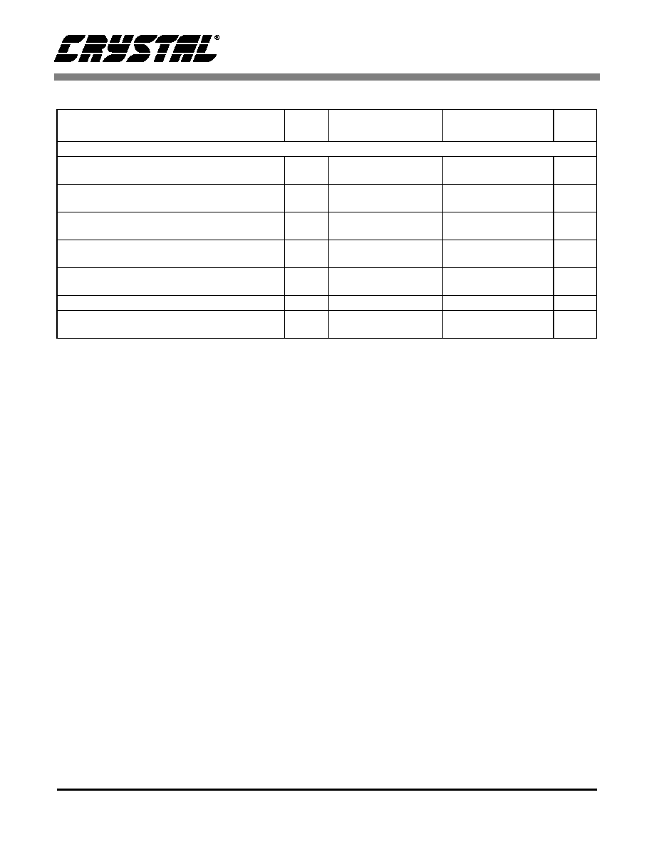
DIGITAL CHARACTERISTICS
(T
A
= 25į C; VL = 1.7 V - 3.6 V; GND = 0 V)
ABSOLUTE MAXIMUM RATINGS
(GND = 0 V; all voltages with respect to ground.)
WARNING: Operation at or beyond these limits may result in permanent damage to the device. Normal operation is
not guaranteed at these extremes.
RECOMMENDED OPERATING CONDITIONS
(GND = 0 V; all voltages with respect to ground.)
Parameters
Symbol Min
Typ
Max
Units
High-Level Input Voltage
V
IH
0.7∑VL
-
-
V
Low-Level Input Voltage
V
IL
-
-
0.3∑VL
V
High-Level Output Voltage
V
OH
0.7∑VL
-
-
V
Low-Level Output Voltage
V
OL
-
-
0.3∑VL
V
Leakage Current
I
in
-
-
Ī10
Ķ
A
Input Capacitance
-
8
-
pF
Parameters
Symbol
Min
Max
Units
DC Power Supplies:
Positive Analog
Digital I/O
VA
VL
-0.3
-0.3
4.0
4.0
V
V
Input Current, Any Pin Except Supplies
I
in
-
Ī10
mA
Digital Input Voltage
V
IND
-0.3
VL+0.4
V
Ambient Operating Temperature (power applied)
T
A
-55
125
įC
Storage Temperature
T
stg
-65
150
įC
Parameters
Symbol Min Typ
Max
Units
Ambient Temperature
T
A
-10
-
70
įC
DC Power Supplies:
Positive Analog
Digital I/O
VA
VL
1.7
1.7
-
-
3.6
3.6
V
V
CS5333
8
DS520PP1
SWITCHING CHARACTERISTICS
(T
A
= -10 to 70į C; VL = 1.7 V - 3.6 V; Inputs: Logic 0 = GND,
Logic 1 = VL, C
L
= 20 pF)
Parameters
Symbol Min Typ
Max
Units
Input Sample Rate
Base Rate Mode
High Rate Mode
Fs
Fs
2
50
-
-
50
100
kHz
kHz
MCLK Pulse Width High
MCLK/LRCK = 1024
8
-
-
ns
MCLK Pulse Width Low
MCLK/LRCK = 1024
8
-
-
ns
MCLK Pulse Width High
MCLK/LRCK = 768
10
-
-
ns
MCLK Pulse Width Low
MCLK/LRCK = 768
10
-
-
ns
MCLK Pulse Width High
MCLK/LRCK = 512
15
-
-
ns
MCLK Pulse Width Low
MCLK/LRCK = 512
15
-
-
ns
MCLK Pulse Width High MCLK / LRCK = 384 or 192
21
-
-
ns
MCLK Pulse Width Low MCLK / LRCK = 384 or 192
21
-
-
ns
MCLK Pulse Width High MCLK / LRCK = 256 or 128
31
-
-
ns
MCLK Pulse Width Low MCLK / LRCK = 256 or 128
31
-
-
ns
Master Mode
SCLK Falling to LRCK Edge
t
slrd
-20
-
20
ns
SCLK Falling to SDATA Valid
t
sdo
0
-
20
ns
SCLK Duty Cycle
40
50
60
%
Slave Mode
LRCK Duty Cycle
-
50
-
%
SCLK Pulse Width Low
t
sclkl
20
-
-
ns
SCLK Pulse Width High
t
sclkh
20
-
-
ns
SCLK Period
Base Rate Mode
High Rate Mode
t
sclkw
t
sclkw
-
-
-
-
ns
ns
SCLK Falling to LRCK Edge
t
slrd
-20
-
20
ns
SCLK Falling to SDATA Valid
Base Rate Mode
High Rate Mode
t
dss
t
dss
-
-
-
-
ns
ns
1
128
(
)
Fs
----------------------
1
64
( )
Fs
------------------
1
(512)Fs
1
(256)Fs
CS5333
DS520PP1
9
SCLK
LRCK
SDATA
t
sclkl
t
slrd
t
dss
MSB
t
sclkh
t
sclkw
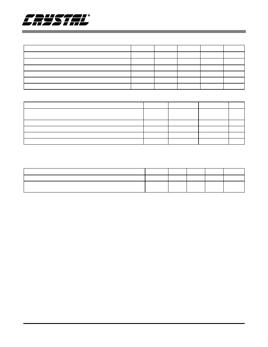
Figure 1. SCLK to LRCK and SDATA, Slave Mode
SCLK
LRCK
SDATA
t
slrd
t
sdo
MSB
MSB-1
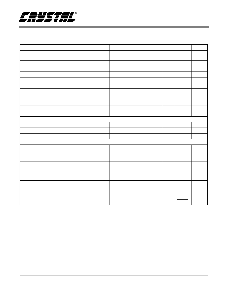
Figure 2. SCLK to LRCK and SDATA, Master Mode

CS5333
10
DS520PP1
2. TYPICAL CONNECTION DIAGRAM
VA
CS5333
1.8 to 3.3 V
Supply
1.0 ĶF
0.1 ĶF
+
1.8 to 3.3 V
Supply
1.0 ĶF
+
VL
5
1
0.47 Ķ F
150
0.47 Ķ F
150
AINL
AINR
**
14
13
0.01 ĶF
0.01 ĶF
0.1 ĶF
GND
6
TST
10
FILT+
REF_GND
1.0 ĶF +
11
12
VQ
1.0 ĶF
15
+
MCLK
LRCK
SCLK
Digital
Audio
Source
SDATA
2
7
3
4
RST
DIF
DIV
Mode
Configuration
16
9
8
47k
Connect to:
∑ VL for Master Mode
∑ GND for Slave Mode
* All capacitors located
on the analog input lines
should be of the type
COG or equivalent.
*
**Optional if analog input
circuit is biased within
Ī5% of CS5333 nominal
bias voltage
**
*
*
*
Figure 3. Typical Connection Diagram

CS5333
DS520PP1
11
3. PIN DESCRIPTION
Interface Power
VL
RST
Reset
Master Clock
MCLK
VQ
Quiescent Voltage
Serial Clock
SCLK
AINL
Left Channel Analog Input
Serial Data Output
SDATA
AINR
Right Channel Analog Input
Analog Power
VA
REF_GND Reference Ground
Ground
GND
FILT+
Positive Voltage Reference
Left Right Clock
LRCK
TST
Test Input
MCLK Divide
DIV
DIF
Digital Interface Format
1
2
3
4
5
6
7
8
5
1
2
6
16
15
14
13
12
11
10
9
1
2
3
4
5
6
7
8
5
1
2
6
16
15
14
13
12
11
10
9
Sample
Rate
(kHz)
MCLK (MHz)
HRM
BRM
128x
192x
256x*
384x*
256x
384x
512x
768x*
1024x*
32
4.0960
6.1440
8.1920
12.2880
8.1920
12.2880
16.3840
24.5760
32.7680
44.1
5.6448
8.4672
11.2896
16.9344
11.2896
16.9344
22.5792
32.7680
45.1584
48
6.1440
9.2160
12.2880
18.4320
12.2880
18.4320
24.5760
36.8640
49.1520
64
8.1920
12.2880
16.3840
24.5760
-
-
-
-
-
88.2
11.2896
16.9344
22.5792
33.8688
-
-
-
-
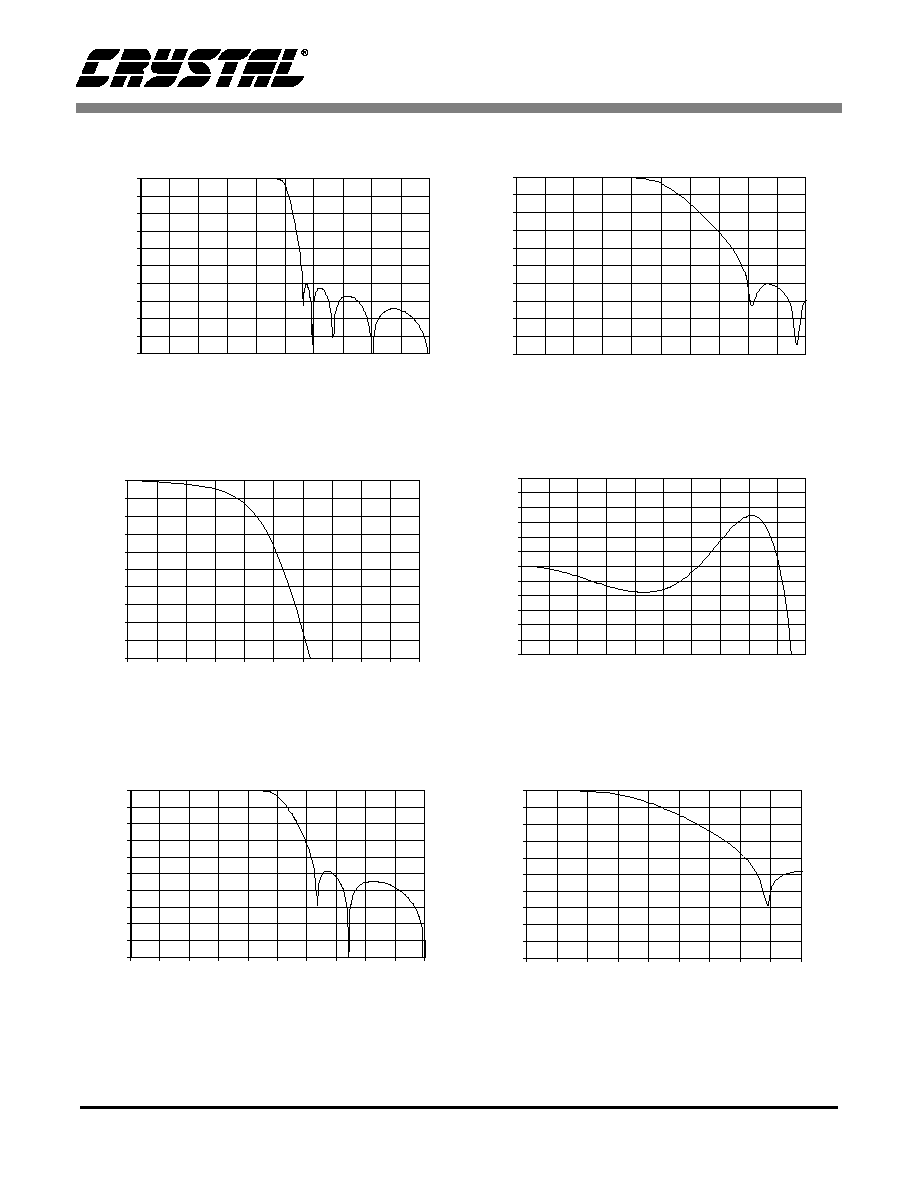
-
96
12.2880
18.4320
24.5760
36.8640
-
-
-
-
-
* DIV= Hi
Table 1. Common Clock Frequencies
Interface Power
1
VL (
Input) - Digital interface power supply. Typically 1.8 to 3.3 VDC.
Master Clock
2
MCLK (
Input) - The master clock frequency must be either 256x, 384x, 512x, 768x or
1024x the input sample rate in Base Rate Mode (BRM) and 128x, 192x, 256x, 384x the
input sample rate in High Rate Mode (HRM). Table 1 illustrates several standard audio
sample rates and the required master clock frequencies.
Serial Clock
3
SCLK (
Input/Output) - Clocks the individual bits of the serial data out of the SDOUT pin.
The required relationship between the Left/Right clock, serial clock and serial data is
defined by the DIF pin.
Serial Audio Data
Out (M/S select)
4
SDATA (
Output) - This pin serves two functions.
First: two's complement MSB-first serial data is output on this pin. The data is clocked out
of SDOUT via the serial clock and the channel is determined by the Left/Right clock. The
required relationship between the Left/Right clock, serial clock and serial data is defined
by the DIF pin.
Second: Master/Slave mode selection is determined, at startup, by a 47 kOhm pullup/pull-
down on this line. A pullup to VL selects Master mode and a pulldown to GND selects
Slave mode.
Analog Power
5
VA (
Input) - Analog power supply. Typically 1.8 to 3.3 VDC.
Ground
6
GND (
Input) - Ground Reference.

CS5333
12
DS520PP1
Left/Right Clock
7
LRCK (
Input/Output) - The Left/Right clock determines which channel is currently being
output on the serial audio data line SDOUT. The frequency of the Left/Right clock must be
at the input sample rate. The required relationship between the Left/Right clock, serial
clock and serial data is defined by the DIF pin.
MCLK Divide
Enable
8
DIV (
Input) - This pin serves different functions in Master and Slave modes.
In Master mode: When high, the chip will enter High Rate Mode; When this pin is low, the
chip will enter Base Rate Mode.
In Slave mode: When high, MCLK is divided internally by 2; When low, MCLK is not
changed.
Digital Interface
Format
9
DIF (
Input) - The required relationship between the Left/Right clock, serial clock and serial
data is defined by the Digital Interface Format.
Test Input
10
TST (
Input) - Must be connected directly to ground.
Positive Voltage
Reference
11
FILT+ (
Output) - Positive reference for internal sampling circuits. An external capacitor is
required from FILT+ to ground, as shown in Figure 3. The recommended value will typi-
cally provide 60 dB of PSRR at 1 kHz and 40 dB of PSRR at 60 Hz. FILT+ is not intended
to supply external current. FILT+ has a typical source impedance of 250 k
and any cur-
rent drawn from this pin will alter device performance.
Reference Ground
12
REF_GND (
Input) - Ground reference for the internal sampling circuits. Must be con-
nected to ground.
Analog Inputs
13,14
AINR, AINL (
Input) - The full scale analog input level is specified in the Analog Character-
istics specification table.
Quiescent Voltage
15
VQ (
Output) - Filter connection for internal A/D converter quiescent reference voltage. A
capacitor must be connected from VQ to ground. VQ is not intended to supply external
current. VQ has a typical source impedance of 250 k
and any current drawn from this pin
will alter device performance.
Reset
16
RST (
Input) - When low the device enters a low power mode and the part is in reset.
When high, the part returns to normal operation within 1024 LRCK cycles.
DIF
DESCRIPTION
0
I
2
S, up to 24-bit data
1
Left Justified, up to 24-bit data
Table 2. Digital Interface Format - DIF
CS5333
DS520PP1
13
4. APPLICATIONS
4.1
Grounding and Power Supply
Decoupling
As with any high resolution converter, the CS5333
requires careful attention to power supply and
grounding arrangements to optimize performance.
Figure 3 show the recommended power arrange-
ment with VA and VL connected to clean supplies.
Decoupling capacitors should be located as close to
the device package as possible.
4.2
Oversampling Modes
The CS5333 operates in one of two oversampling
modes. Base Rate Mode supports input sample
rates up to 50 kHz while High Rate Mode supports
input sample rates up to 100 kHz. See Table 1 for
more details.
4.3
Recommended Power-up Sequence
1) Hold RST low until the power supply, master,
and left/right clocks are stable. In this state, VQ
will remain low.
2) Bring RST high. The device will remain in a
low power state with VQ low and will initiate
the power-up sequence. This power-up se-
quence takes approximately 1024 LRCK cycles
to complete.
4.4
Master/Slave Mode
In Master, Base Rate Mode (Pull-up on SDATA,
DIV=0), the CS5333 requires a 256x MCLK and
provide a 64x SCLK. In Master, High Rate Mode
(Pull-up on SDATA, DIV=1), the CS5333 requires
a 128x MCLK and provide a 64x SCLK. The vari-
ous clocking ratios required in Slave Mode (Pull-
down on SDATA) are listed under the description
of MCLK, on page 11.
CS5333
14
DS520PP1
-100
-90
-80
-70
-60
-50
-40
-30
-20
-10
0
0
0.1
0.2
0.3
0.4
0.5
0.6
0.7
0.8
0.9
1
Frequency (normalized to Fs)
A
m
pl
i
t
ud
e
dB
-100
-90
-80
-70
-60
-50
-40
-30
-20
-10
0
0.4
0.42
0.44
0.46
0.48
0.5
0.52
0.54
0.56
0.58
0.6
Frequency (normalized to Fs)
A
m
pl
i
t
ude
dB
Figure 4. Base-Rate Stopband Rejection
Figure 5. Base-Rate Transition Band
-0.3
-0.25
-0.2
-0.15
-0.1
-0.05
0
0.05
0.1
0.15
0.2
0.25
0.3
0
0.05
0.1
0.15
0.2
0.25
0.3
0.35
0.4
0.45
0.5
Frequency (normalized to Fs)
A
m
pl
i
t
ude
dB
Figure 6. Base-Rate Transition Band (Detail)
Figure 7. Base-Rate Passband Ripple
-10
-9
-8
-7
-6
-5
-4
-3
-2
-1
0
0.45
0.46
0.47
0.48
0.49
0.5
0.51
0.52
0.53
0.54
0.55
Frequency (normalized to Fs)
A
m
pl
i
t
ude
d
B
-100
-90
-80
-70
-60
-50
-40
-30
-20
-10
0
0
0.1
0.2
0.3
0.4
0.5
0.6
0.7
0.8
0.9
1
Frequency (normalized to Fs)
A
m
pl
i
t
ude
dB
-100
-90
-80
-70
-60
-50
-40
-30
-20
-10
0
0.4
0.43
0.46
0.49
0.52
0.55
0.58
0.61
0.64
0.67
Frequency (normalized to Fs)
A
m
pl
i
t
ude
dB
Figure 8. High-Rate Stopband Rejection
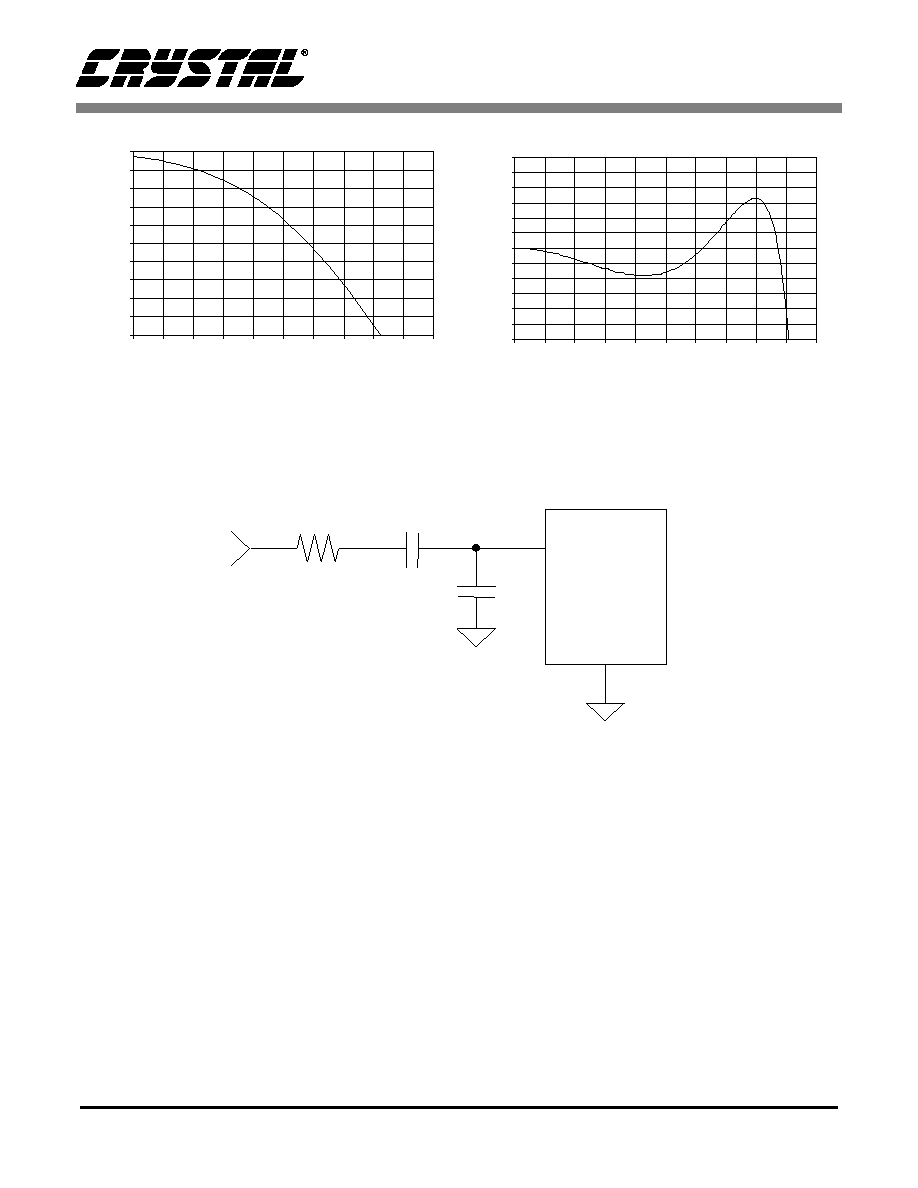
Figure 9. High-Rate Transition Band
CS5333
DS520PP1
15
-10
-9
-8
-7
-6
-5
-4
-3
-2
-1
0
0.45
0.46
0.47
0.48
0.49
0.5
0.51
0.52
0.53
0.54
0.55
Frequency (normalized to Fs)
A
m
pl
i
t
ude
d
B
-0.3
-0.25
-0.2
-0.15
-0.1
-0.05
0
0.05
0.1
0.15
0.2
0.25
0.3
0
0.05
0.1
0.15
0.2
0.25
0.3
0.35
0.4
0.45
0.5
Frequency (normalized to Fs)
A
m
pl
i
t
ude
dB
Figure 10. High-Rate Transition Band (Detail)
Figure 11. High-Rate Passband Ripple
GND
AINx
150
0.47 ĶF
0.01 ĶF
Figure 12. Line Input Test Circuit
CS5333
16
DS520PP1
LRCK
SCLK
Left Channel
Right Channel
SDATA
+3 +2 +1 LSB
+5 +4
MSB -1 -2 -3 -4 -5
+3 +2 +1 LSB
+5 +4
MSB -1 -2 -3 -4
I
2
S, up to 24-Bit Data. Data Valid on Rising Edge of
SCLK
Figure 13. CS5333 - Serial Audio Format 0
LRCK
SCLK
Left Channel
Right Channel
SDATA
+3 +2 +1 LSB
+5 +4
MSB -1 -2 -3 -4 -5
+3 +2 +1 LSB
+5 +4
MSB -1 -2 -3 -4
Left Justified, up to 24-Bit Data. Data Valid on Rising
Edge of SCLK.
Figure 14. CS5333 - Serial Audio Format 1

CS5333
DS520PP1
17
5. PARAMETER DEFINITIONS
Total Harmonic Distortion + Noise (THD+N)
The ratio of the rms value of the signal to the rms sum of all other spectral components over the specified
bandwidth (typically 10 Hz to 20 kHz), including distortion components. Expressed in decibels.
Dynamic Range
The ratio of the full scale rms value of the signal to the rms sum of all other spectral components over the
specified bandwidth. Dynamic range is a signal-to-noise measurement over the specified bandwidth
made with a -60 dBFS signal. 60 dB is then added to the resulting measurement to refer the measurement
to full scale. This technique ensures that the distortion components are below the noise level and do not
effect the measurement. This measurement technique has been accepted by the Audio Engineering So-
ciety, AES17-1991, and the Electronic Industries Association of Japan, EIAJ CP-307.
Interchannel Isolation
A measure of crosstalk between the left and right channels. Measured for each channel at the converter's
output with all zeros to the input under test and a full-scale signal applied to the other channel. Units in
decibels.
Interchannel Gain Mismatch
The gain difference between left and right channels. Units in decibels.
Gain Error
The deviation from the nominal full scale analog output for a full scale digital input.
Gain Drift
The change in gain value with temperature. Units in ppm/įC.
6. REFERENCES
1. "How to Achieve Optimum Performance from Delta-Sigma A/D & D/A Converters" by Steven Harris.
Paper presented at the 93rd Convention of the Audio Engineering Society, October 1992.
2. CDB5333 Evaluation Board Datasheet.
CS5333
18
DS520PP1
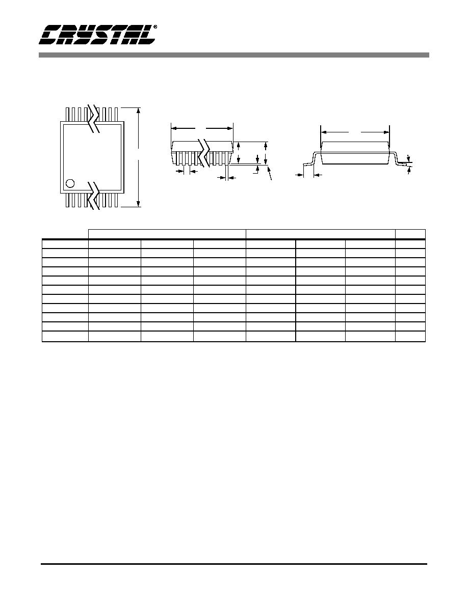
7. PACKAGE DIMENSIONS
Notes: 1. "D" and "E1" are reference datums and do not included mold flash or protrusions, but do include mold
mismatch and are measured at the parting line, mold flash or protrusions shall not exceed 0.20 mm per
side.
2. Dimension "b" does not include dambar protrusion/intrusion. Allowable dambar protrusion shall be
0.13 mm total in excess of "b" dimension at maximum material condition. Dambar intrusion shall not
reduce dimension "b" by more than 0.07 mm at least material condition.
3. These dimensions apply to the flat section of the lead between 0.10 and 0.25 mm from lead tips
INCHES
MILLIMETERS
NOTE
DIM
MIN
NOM
MAX
MIN
NOM
MAX
A
--
--
0.043
--
--
1.10
A1
0.002
0.004
0.006
0.05
--
0.15
A2
0.03346
0.0354
0.037
0.85
0.90
0.95
b
0.00748
0.0096
0.012
0.19
0.245
0.30
2,3
D
0.193
0.1969
0.201
4.90
5.00
5.10
1
E
0.248
0.2519
0.256
6.30
6.40
6.50
E1
0.169
0.1732
0.177
4.30
4.40
4.50
1
e
--
0.026 BSC
--
--
0.065 BSC
--
L
0.020
0.024
0.028
0.50
0.60
0.70
0į
4į
8į
0į
4į
8į
JEDEC #: MO-153
Controlling Dimension is Millimeters
16L TSSOP (4.4 mm BODY) PACKAGE DRAWING
E
N
1 2 3
e
b
2
A1
A2
A
D
SEATING
PLANE
E1
1
L
SIDE VIEW
END VIEW
TOP VIEW

∑ Notes ∑