 | –≠–ª–µ–∫—Ç—Ä–æ–Ω–Ω—ã–π –∫–æ–º–ø–æ–Ω–µ–Ω—Ç: CDB5360 | –°–∫–∞—á–∞—Ç—å:  PDF PDF  ZIP ZIP |
Document Outline
- CDB5334/35/60: Evaluation Board
- Features
- Description
- CDB5334/35/60 SYSTEM OVERVIEW
- Power Supply Circuitry and Grounding
- Reset Circuit and Offset Calibration
- Input Buffer and Protection Circuits
- CS5334, CS5335, and CS5360 A/D Converters
- CS8402A Digital Audio Interface
- Serial Output Interface
- ALTERA PLD AND PEAK SIGNAL LEVEL LEDS
- CS8402A Format Configuration
- CS8402A MCLK Generation
- Decoding PSL bits / Driving LEDs
- GROUNDING AND POWER SUPPLY DECOUPLING
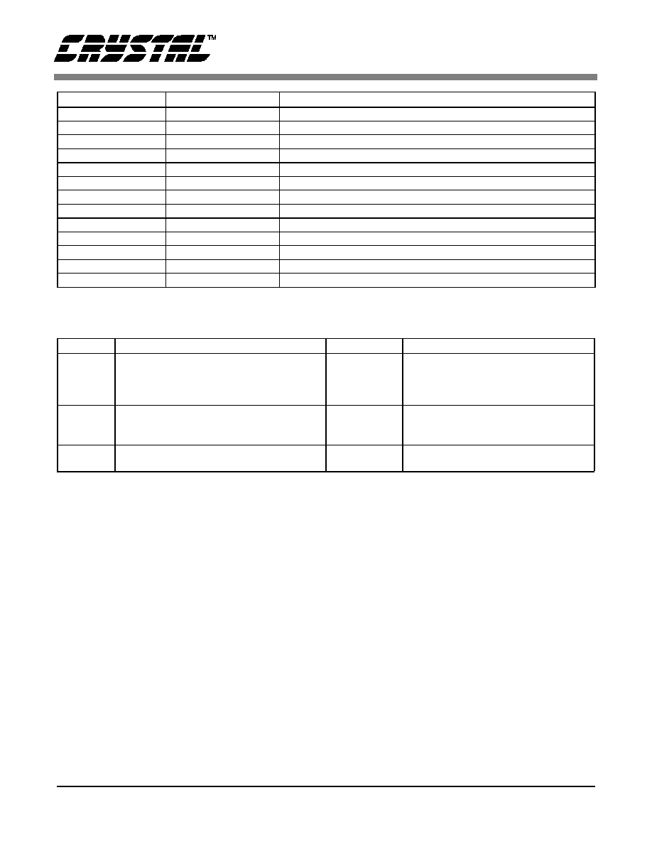
- Table 1. System Connections
- Table 2. Jumper Selectable Options
- Table 3. Switch Definitions
- Table 4. CS8402A Switch Definitions - Consumer Mode
- Table 5. CS8402A Switch Definitions - Professional Mode
- Figure 1. System Block Diagram and Signal Flow
- Figure 2. Power Supply and Reset Circuitry
- Figure 3. Analog Input Buffer
- Figure 4. CS5334, CS5335, and CS5360 Connections
- Figure 5. CS8402A Digital Audio Transmitter and Connections
- Figure 6. I/O Interface for Clocks and Data
- Figure 7. Decoupling Caps for PLD
- Figure 8. Altera PLD and Display LEDs
- Figure 9. CDB5334/35/60 Component side (top)
- Figure 10. CDB5334/35/60 Component side (bottom)
- Figure 11. CDB5334/35/60 Solder side (bottom)

Preliminary Product Information
This document contains information for a new product.
Cirrus Logic reserves the right to modify this product without notice.
1
Copyright
©
Cirrus Logic, Inc. 1997
(All Rights Reserved)
Cirrus Logic, Inc.
Crystal Semiconductor Products Division
P.O. Box 17847, Austin, Texas 78760
(512) 445 7222 FAX: (512) 445 7581
http://www.crystal.com
CDB5334/35/60
Evaluation Board for CS5334/CS5335/CS5360
Features
l
Demonstrates recommended layout and
grounding arrangements
l
CS8402A Generates AES/EBU, S/PDIF, &
EIAJ-340 Compatible Digital Audio
l
Buffered Serial Output Interface
l
Digital and Analog Patch Areas
l
On-board or externally supplied system
timing
Description
The CDB5334/35/60 evaluation board is an excellent
means for quickly evaluating the CS5334, CS5335, or
CS5360 stereo A/D converters. Evaluation requires a
digital signal processor, a low distortion analog signal
source and a power supply. Analog inputs are provided
via XLR connectors for both channels.
Also included is a CS8402A digital audio interface trans-
mitter which generates AES/EBU, S/PDIF, and EIAJ-340
compatible audio data. The digital audio data is available
via RCA phono, and optical connectors.
The evaluation board may also be configured to accept
external timing signals for operation in a user application
during system development.
ORDERING INFO
CDB5334/35/60
I
OCT `97
DS194DB3

CDB5334/35/60
2 DS194DB3
CDB5334/35/60 SYSTEM OVERVIEW
The CDB5334/35/60 evaluation boards are an ex-
cellent means of quickly evaluating the CS5334,
CS5335, or CS5360. The CS8402A digital audio
interface transmitter provides an easy interface to
digital audio signal processors, including the ma-
jority of digital audio test equipment. The evalua-
tion board has been designed to accept an analog
input, and provide optical and coaxial digital out-
puts. The evaluation board also allows the user to
access clocks and data through a 10-pin header for
system development. In addition, the evaluation
board supports the input level monitoring function
provided by the CS5334, CS5335, and CS5360.
The Peak Signal Level bits are displayed on bar-
graph LEDs or 7 segment displays for both left and
right channels.
The CDB5334/35/60 schematic has been parti-
tioned into 7 schematics shown in Figures 2
through 8. Each partitioned schematic is represent-
ed in the system diagram shown in Figure 1. Notice
that the system diagram also includes the connec-
tions between the partitioned schematics.
Power Supply Circuitry and Grounding
Power is supplied to the evaluation board by six
binding posts as shown in Figure 2. +5VA provides
5 Volt power to the converter and the reset circuit-
ry. The ±12 V binding posts provide power to the
analog input buffer. C1-C3 and C5-C7 provide
general power supply filtering for the analog sup-
plies. Z1-Z3 are transient suppression diodes which
also provide protection from incorrectly connected
power supply leads. +5VD supplies 5 Volt power
to the digital section of the board. C41 and C10 pro-
vide general power supply filtering. Z4 is a tran-
sient suppressor.
Localized decoupling for the CS5334, CS5335, or
CS5360 is provided by C16, C17, C32, and C33, as
shown in Figure 4. R10, C16, and C32 form a low
pass filter which isolates VA+ from noise on VD+.
The evaluation board uses separate analog and dig-
ital ground planes which are joined together under-
neath resistors R6, R41, and R52-R55. This
arrangement isolates the analog circuitry from the
digital logic.
Reset Circuit and Offset Calibration
Two methods of placing the CS5334, CS5335, or
CS5360 into power-down mode are provided on
the evaluation board. The CAL switch, shown in
Figure 8, pulls the DIF0 and DIF1 lines high on the
CS5334, CS5335, or CS5360, thus placing the
ADC into power-down mode. Releasing the CAL
switch causes the DIF0 and DIF1 settings to be re-
stored, upon which an initialization sequence be-
gins, as described in the CS5334/CS5335 and
CS5360 data sheets.
The reset circuit provided on the evaluation board
is shown in Figure 2. Upon power up, this circuit
sends a reset to the RST pin of the CS5334,
CS5335, or CS5360. Power-down, followed by
offset calibration, can also be performed by press-
ing and then releasing the RST switch. It should be
noted that only the RST method of powering down
the CS5334, CS5335, or CS5360 will include the
decision of master or slave operation.
Input Buffer and Protection Circuits
The differential input circuit shown in Figure 3 is
well-suited for the CS5334, CS5335, and CS5360
in professional applications. The circuit will accept
a differential or single-ended signal of either polar-
ity and provide a differential signal with the proper
DC offset to the CS5334, CS5335, or CS5360. The
circuit also incorporates 6 dB of attenuation to
scale down professional input levels to the input
voltage range of the CS5334, CS5335, or CS5360.
A nominal input level of 4 Volts rms to the evalua-
tion board will achieve a full scale digital output
from the CS5334, CS5335, or CS5360. The com-
mon mode rejection of the system is limited by the
passive component matching of the input buffer

CDB5334/35/60
DS194DB3 3
circuit. The analog input connector is a standard fe-
male XLR with Pin 2 positive, Pin 3 return, and Pin
1 shield.
R1, R5, and C8 form an RC network which pro-
vides anti-alias filtering and the optimum source
impedance for the CS5334, CS5335, or CS5360
right channel inputs. R2, R3, and C42 duplicate this
function for the left channel.
Space has been left on the evaluation board for in-
put protection diodes D1-D4 on the right channel,
and D8-D11 on the left channel, shown in Figure 3.
These diodes are optional as the CS5334, CS5335,
and CS5360 are able to withstand input currents of
100mA maximum, as stated in the
CS5334/CS5335 and CS5360 data sheets. The out-
put current from the op-amp used in the analog fil-
ter on the evaluation board is not able to deliver a
current that exceeds 100mA. Input protection di-
odes are recommended if there is a possibility that
over-range signals could be applied at the ADC in-
puts which exceed this level. See the application
note, "A/D Converter Input Protection Techniques"
in the 1994 Crystal Semiconductor Audio Da-
tabook.
CS5334, CS5335, and CS5360 A/D
Converters
The CS5334, CS5335, and CS5360 A/D converters
are shown in Figure 4. A description of these devic-
es are included in the CS5334/CS5335 and CS5360
data sheets.
CS8402A Digital Audio Interface
Figure 5 shows the circuitry for the CS8402A dig-
ital audio interface transmitter. The CS8402A can
implement AES/EBU, S/PDIF, and EIAJ-340 in-
terface standards. The Digital Interface Format
(DIF) for the transmitter is set automatically to
match the format chosen for the CS5334, CS5335,
or CS5360 (the DIF is selected by the DIF1 and
DIF0 switches on SW1, as defined in Table 3).
SW2 provides 8 DIP switches to select various
modes and bits for the CS8402A; switch defini-
tions and the default settings for SW2 are listed in
Tables 4 and 5. Digital outputs are provided on an
RCA connector via isolation transformer and on an
optical transmitter. For more detailed information
on the CS8402A and the digital audio standards,
see the CS8401A/CS8402A data sheet.
Serial Output Interface
A serial output interface is provided on HDR2, as
shown in Figure 6. When the SMODE1 and
SMODE2 jumpers, defined in Table 2, are set to
the MASTER position, MCLK, SCLK, LRCK,
SDATA, and FRAME signals are outputs. When
the SMODE1 and SMODE2 jumpers are in the
SLAVE position, MCLK, SDATA, and FRAME
are outputs, while SCLK and LRCK become in-
puts. Hence, in SLAVE mode, the SCLK and
LRCK signals must be externally derived from
MCLK to run the ADC. All signals are buffered in
order to isolate the converter from external circuit-
ry. Signal buffering is provided by a 74HCT243
transceiver (U10) and a 74HCT541 buffer (U11).
ALTERA PLD AND PEAK SIGNAL
LEVEL LEDS
The Altera EPM7128 programmable logic device
(PLD), shown in Figure 8, is designed to support
three major features on the evaluation board. First,
it automatically configures the CS8402A transmit-
ter to accept the Digital Interface Format chosen for
the CS5334, CS5335, or CS5360. Second, the PLD
provides a 128x Fs master clock for the CS8402A.
Third, it decodes and updates the Peak Signal Level
(PSL) bits which give information about the ampli-
tude of the input signal.
CS8402A Format Configuration
The CS5334, CS5335, and CS5360 support three
Digital Interface Formats for both master and slave
configurations. Format 0 has valid data on the ris-
ing edge of SCLK. The CS8402A transmitter has
no corresponding mode which matches Format 0,

CDB5334/35/60
4 DS194DB3
but inverting the SCLK so that data is valid on the
falling edge of SCLK will make the Format 0 inter-
face lines match the Format 1 interface lines on the
CS8402A. The PLD configures the CS8402A to
Format 1 and performs SCLK inversion automati-
cally when the DIF1, DIF0 switches on SW1 are set
to 00.
Digital Interface Format 1 on the CS5334, CS5335,
and CS5360 has valid data on the falling edge of
SCLK. This interface format matches Format 1 on
the CS8402A, so no modification is performed on
the digital interface lines. The PLD configures the
CS8402A to FORMAT 1 and passes the interface
lines from the CS5334, CS5335, or CS5360
through to the CS8402A unchanged when the
DIF1, DIF0 switches are set to 01.
Digital Interface Format 2 is the I2S compatible
mode. It matches Format 4 on the transmitter. The
PLD configures the CS8402A to Format 4 and
passes the interface lines from the CS5334,
CS5335, or CS5360 through to the CS8402A un-
changed when the DIF1, DIF0 switches are set to
10.
CS8402A MCLK Generation
When the CDB5334/35/60 is set up for SLAVE
mode, the crystal oscillator (U5) can be 256x,
384x, or 512x Fs. The CS8402A requires a master
clock frequency of 128x Fs to operate. The PLD
can be configured to divide MCLK_5335 (the os-
cillator output) by 2, 3, or 4 to generate
MCLK_8402, thus accommodating the various
possible frequencies of the oscillator. The switches
on SW1 labeled MCLK_S1 and MCLK_S0 select
the degree of clock division as defined in Table 3.
Decoding PSL bits / Driving LEDs
The PLD decodes and displays the Peak Signal
Level bits for both High Resolution and Bargraph
modes (for detailed information on the PSL bits,
see the CS5334/CS5335 and CS5360 datasheets).
When the TMODE1 and TMODE2 jumpers, de-
fined in Table 2, are set to BARGRAPH, the PLD
decodes the PSL bits and drives bargraph LEDs for
the left and right channels. When the TMODE1 and
TMODE2 jumpers are set to HI RES (High Reso-
lution mode), the PLD drives the 7 segment dis-
plays for left and right channels.
The PLD also provides a Peak Update (PU) signal,
which adjusts the rate at which the PSL bits are up-
dated. Four settings provide update rates ranging
from 42 ms to 2.7 s (for a 48 kHz sample rate). The
switches on SW1 labeled PU_S1 and PU_S0 select
the PU frequency as shown in Table 3.
GROUNDING AND POWER SUPPLY
DECOUPLING
The CS5334, CS5335, and CS5360 require careful
attention to power supply and grounding arrange-
ments to optimize performance. Figure 4 shows the
recommended power arrangements. The CS5334,
CS5335, or CS5360 is positioned over the analog
ground plane, near the digital/analog ground plane
split, to minimize the distance that the clocks trav-
el. The series resistors are present on the clock and
data lines to reduce the effects of transient currents
when driving a capacitive load in MASTER mode,
and to reduce clock overshoot when applying ex-
ternal clocks to the ADC in SLAVE mode.
This layout technique is used to minimize digital
noise and to insure proper power supply match-
ing/sequencing. The decoupling capacitors are lo-
cated as close to the ADC as possible. Extensive
use of ground plane fill on both the analog and dig-
ital sections of the evaluation board yield large re-
ductions in radiated noise effects.
CDB5334/35/60
DS194DB3 5
Table 1. System Connections
Table 2. Jumper Selectable Options
CONNECTOR INPUT/OUTPUT SIGNAL PRESENT
+5VA input +5 Volts for analog section
+5VD input +5 Volts for digital section
±12V input ±12 Volts for analog input
AGND input analog ground connection from power source
DGND input digital ground connection from power source
AINL input left channel differential/single ended analog input
AINR input right channel differential/single ended analog input
LRCK, SCLK input/output I/O for serial and left/right clocks
MCLK output master clock output
SDATA output serial data output
FRAME output framing signal output for PSL bits
coaxial output output CS8420A digital output via transformer
optical output output CS8420A digital output via optical transmitter
JUMPER PURPOSE POSITION FUNCTION SELECTED
SMODE1,
SMODE2
Selects master/slave operation for
CS5334, CS5335, and CS5360 and I/O
status of HDR2. SMODE1 and SMODE2
should always be set to the same position.
*MASTER
SLAVE
Timing generation onboard.
External clock generation, derived from
MCLK.
TMODE1,
TMODE2
Selects the functionality of the PSL bits.
TMODE1 and TMODE2 should always be
set to the same position.
HI RES
*BARGRAPH
PSL bits display the input level
PSL bits display the bargraph
HPSEL Enables or disables the input highpass filter
on the CS5334, CS5335, and CS5360
DEFEAT
*ENABLE
Defeats highpass filter
Enables highpass filter