Copyright
�
Cirrus Logic, Inc. 2004
(All Rights Reserved)
http://www.cirrus.com
F
EATURES
20-Pin TSSOP package
1.8 V to 3.3 V supply
24-bit conversion / 96 kHz sample rate
98 dB dynamic range at 3 V supply
-88 dBFS THD+N
Low power consumption
� 11 mW at 1.8 V
Up to 32 dB gain
� 20 dB gain step
� 12 dB variable input gain, 1 dB steps
� Changes made at zero crossings
Stereo inputs
Digital volume control
� 96 dB attenuation, 1 dB step size
� Mute
� Soft ramping
2:1 Input mux
D
ESCRIPTION
The CS53L32A is a highly integrated, 24-bit, 96 kHz au-
dio ADC providing stereo analog-to-digital converters
using delta-sigma conversion techniques. This device in-
cludes volume control and line level inputs in a 20-pin
TSSOP package.
The CS53L32A is based on delta-sigma modulation al-
lowing infinite adjustment of the sample rate between
2 kHz and 100 kHz simply by changing the master clock
frequency.
The CS53L32A contains adjustable analog gain, a 2:1
input mux, and digital attenuation.
The CS53L32A operates from a +1.8 V to +3.3 V supply.
These features are ideal for portable MP3 players, MD
recorders/players, digital camcorders, PDAs, set-top
boxes, and other portable systems that require extreme-
ly low power consumption in a minimum of space.
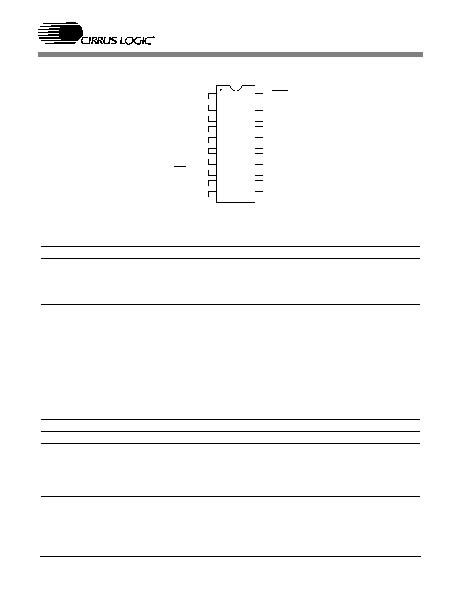
ORDERING INFORMATION
CS53L32A-KZ
20-pin TSSOP
-10 to 70 �C
CS53L32A-KZZ 20-pin TSSOP
-10 to 70 �C Lead free
CS53L32A-BZ
20-pin TSSOP
-40 to 85 �C
CDB53L32A
Evaluation Board
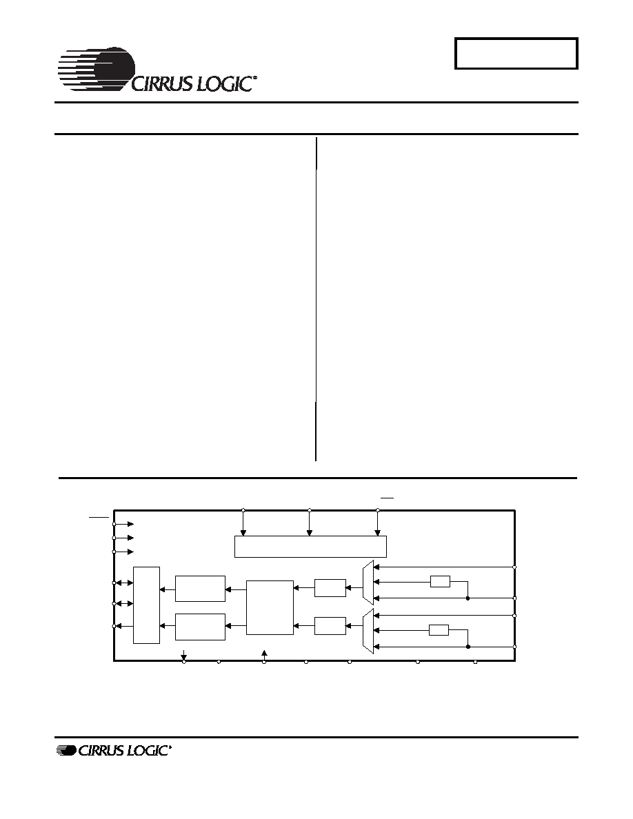
I I
SCL/CCLK/
SDA/CDIN/DIF
Control Port
RST
LRCK
SCLK
Se
r
i
a
l
P
o
r
t
MCLK
VA
GND
VQ
FILT+ REF_GND
AIN_L1
AIN_L2
AIN_R1
AIN_R2
ADC
ADC
Digital
Filters
Attenuator
0-96 dB
SDOUT
AD0/CS/DIV
Attenuator
0-96 dB
Gain
Gain
AFLTL
AFLTR
ChSEL
VL
CS53L32A
Low Voltage, Stereo A/D Converter
OCT `04
DS513F1

CS53L32A
2
DS513F1
TABLE OF CONTENTS
1. CHARACTERISTICS/SPECIFICATIONS ................................................................................. 4
ANALOG CHARACTERISTICS ................................................................................................ 4
ANALOG CHARACTERISTICS ................................................................................................ 5
POWER AND THERMAL CHARACTERISTICS....................................................................... 8
DIGITAL CHARACTERISTICS ................................................................................................. 9
ABSOLUTE MAXIMUM RATINGS ........................................................................................... 9
RECOMMENDED OPERATING CONDITIONS ....................................................................... 9
SWITCHING CHARACTERISTICS ........................................................................................ 10
SWITCHING CHARACTERISTICS - CONTROL PORT - TWO WIRE MODE....................... 12
SWITCHING CHARACTERISTICS - CONTROL PORT - SPI MODE.................................... 13
2. TYPICAL CONNECTION DIAGRAM .................................................................................... 14
3. REGISTER QUICK REFERENCE .......................................................................................... 15
3.1 I/O and Power Control (address 01h) ............................................................................... 15
3.2 Interface Control (address 02h) ........................................................................................ 15
3.3 Analog I/O Control (address 03h) ..................................................................................... 16
3.4 Left Channel Digital Volume Control (address 04h).......................................................... 17
3.5 Right Channel Digital Volume Control (address 05h) ....................................................... 17
3.6 Analog Gain Control (address 06h) .................................................................................. 17
3.7 Clip Detection Status (address 07h) ................................................................................. 17
4. REGISTER DESCRIPTION .................................................................................................... 18
4.1 Gain Enable ...................................................................................................................... 18
4.2 Analog Input Multiplexer ................................................................................................... 18
4.3 Power-Down ..................................................................................................................... 19
4.4 Control Port Enable........................................................................................................... 19
4.5 Master Clock Divide .......................................................................................................... 20
4.6 Master Clock Ratio............................................................................................................ 20
4.7 Master Mode ..................................................................................................................... 21
4.8 Digital Interface Format..................................................................................................... 21
4.9 Left/Right Channel Mute ................................................................................................... 22
4.10 Soft Ramp and Zero Cross Enable ................................................................................. 22
4.11 Independent Volume Control Enable .............................................................................. 23
4.12 Left Channel Volume = Right Channel Volume .............................................................. 24
4.13 High-Pass Filter Freeze .................................................................................................. 24
4.14 Volume Control ............................................................................................................... 25
4.15 Left/Right Analog Gain.................................................................................................... 26
4.16 Clip Detection.................................................................................................................. 26
5. PIN DESCRIPTION ................................................................................................................. 27
6. PIN DESCRIPTION ................................................................................................................. 28
6. PIN DESCRIPTION ................................................................................................................. 28
6. APPLICATIONS ...................................................................................................................... 30
6.1 Grounding and Power Supply Decoupling ....................................................................... 30
6.2 Oversampling Modes ....................................................................................................... 30
6.3 Recommended Power-up Sequence ............................................................................... 30
7. CONTROL PORT INTERFACE ............................................................................................. 30
7.1 SPI Mode ......................................................................................................................... 30
7.2 Two Wire Mode ................................................................................................................ 31
7.3 Memory Address Pointer (MAP) ....................................................................................... 31
8. PARAMETER DEFINITIONS .................................................................................................. 38
9. REFERENCES ........................................................................................................................ 38
10. PACKAGE DIMENSIONS ..................................................................................................... 39
11. CHANGE HISTORY .............................................................................................................. 40

CS53L32A
DS513F1
3
LIST OF FIGURES
Figure 1. SCLK to LRCK and SDOUT, Slave Mode ..................................................................... 11
Figure 2. SCLK to LRCK and SDOUT, Master Mode ................................................................... 11
Figure 3. Relationship Required Between LRCK and MCLK in Slave Mode ................................ 11
Figure 4. Control Port Timing - Two Wire Mode............................................................................ 12
Figure 5. Control Port Timing - SPI Mode ..................................................................................... 13
Figure 6. Typical Connection Diagram .......................................................................................... 14
Figure 7. Control Port Timing, SPI Mode ...................................................................................... 32
Figure 8. Control Port Timing, Two Wire Mode............................................................................. 32
Figure 9. Base-Rate Stopband Rejection...................................................................................... 33
Figure 10. Base-Rate Transition Band.......................................................................................... 33
Figure 11. Base-Rate Transition Band (Detail) ............................................................................. 33
Figure 12. Base-Rate Passband Ripple........................................................................................ 33
Figure 13. High-Rate Stopband Rejection .................................................................................... 33
Figure 14. High-Rate Transition Band........................................................................................... 33
Figure 15. High-Rate Transition Band (Detail) .............................................................................. 34
Figure 16. High-Rate Passband Ripple......................................................................................... 34
Figure 17. Line Input Test Circuit .................................................................................................. 34
Figure 18. CS53L32A Control Port Mode - Serial Audio Format 0 (I
2
S) ....................................... 34
Figure 19. CS53L32A Control Port Mode - Serial Audio Format 1 ............................................... 35
Figure 20. CS53L32A Control Port Mode - Serial Audio Format 3 ............................................... 35
Figure 21. CS53L32A Control Port Mode - Serial Audio Format 4 ............................................... 35
Figure 22. CS53L32A Control Port Mode - Serial Audio Format 5 ............................................... 36
Figure 23. CS53L32A Control Port Mode - Serial Audio Format 6 ............................................... 36
Figure 24. CS53L32A Stand-Alone Mode - Serial Audio Format 0 (I
2
S) ...................................... 36
Figure 25. CS53L32A Stand-Alone Mode - Serial Audio Format 1............................................... 37
LIST OF TABLES
Table 1. Analog Input Options....................................................................................................... 18
Table 2. Power-Down Enable ....................................................................................................... 19
Table 3. Control Port Enable......................................................................................................... 19
Table 4. Master Clock Divide Select ............................................................................................. 20
Table 5. MCLK/LRCK Ratios ........................................................................................................ 20
Table 6. Master/Slave Mode Selection ......................................................................................... 21
Table 7. Digital Interface Format................................................................................................... 21
Table 8. Left/Right Channel Mute Enable ..................................................................................... 22
Table 9. Analog Volume Control ................................................................................................... 23
Table 10. Digital Volume Control .................................................................................................. 23
Table 11. Independent Volume Control Enable ............................................................................ 23
Table 12. High-Pass Filter Enable ................................................................................................ 24
Table 13. Example Volume Settings ............................................................................................. 25
Table 14. Example Gain Settings.................................................................................................. 26
Table 15. Clip Detection Status Bits.............................................................................................. 26
Table 16. Common Clock Frequencies......................................................................................... 28
Table 17. Digital Interface Format - DIF (Stand-Alone Mode)....................................................... 28
Table 18. Channel Select Options ................................................................................................ 28
Table 19. Revision Table .............................................................................................................. 40
CS53L32A
4
DS513F1
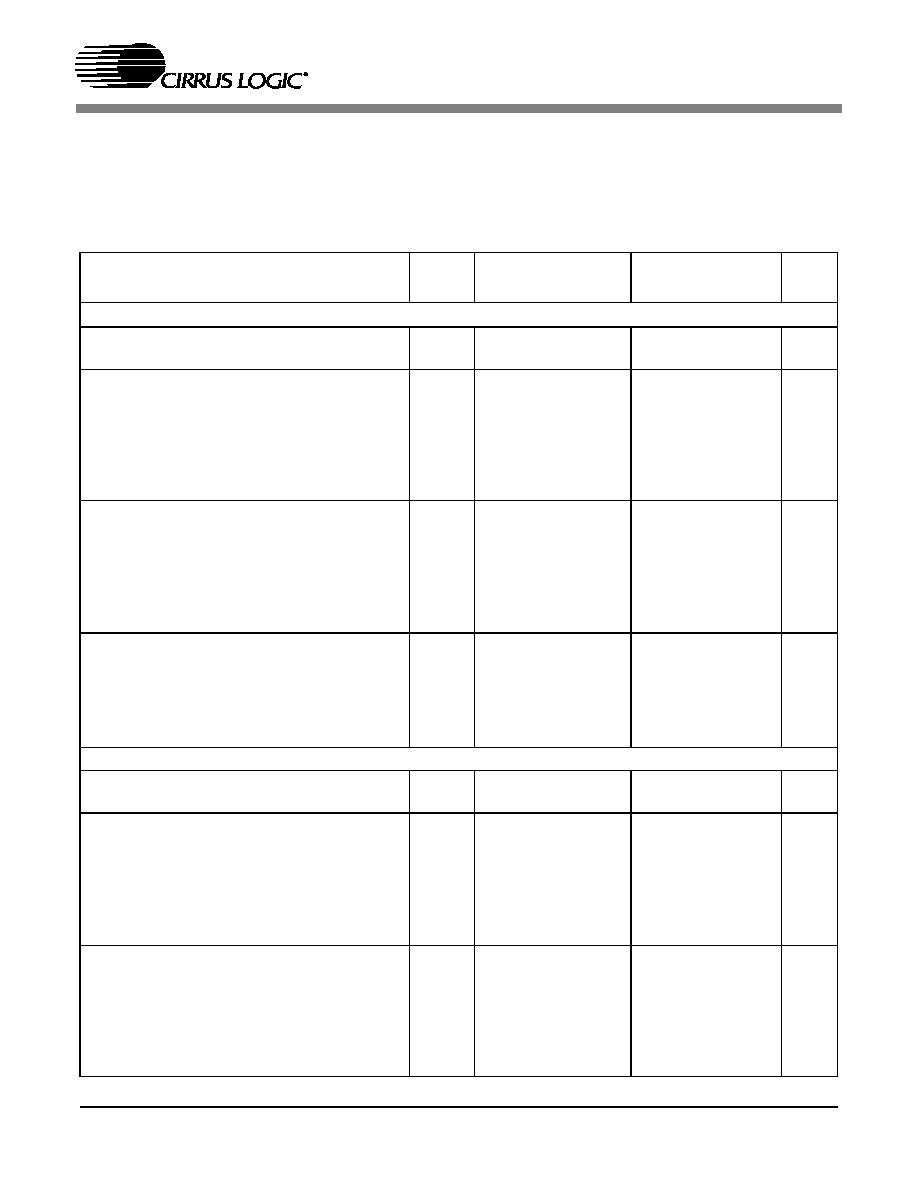
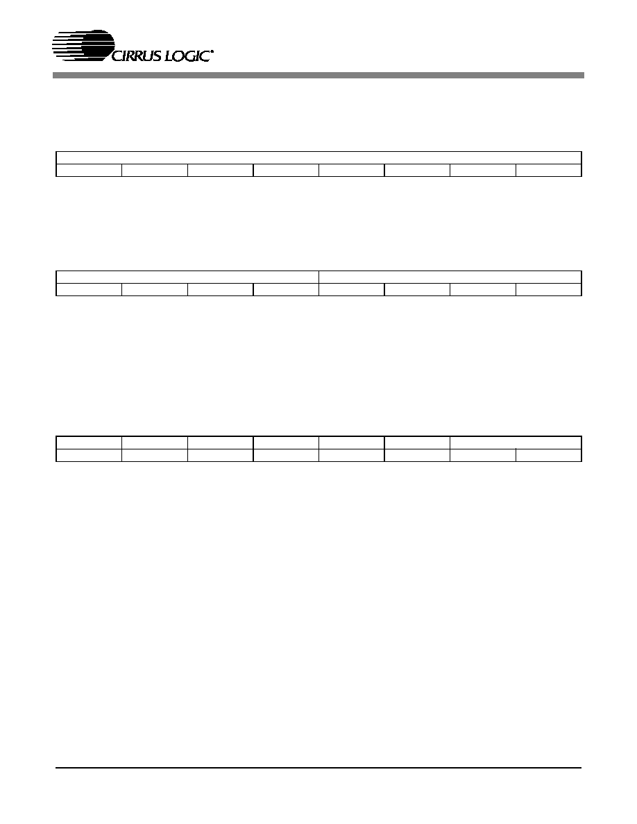
1.
CHARACTERISTICS/SPECIFICATIONS
ANALOG CHARACTERISTICS
(T
A
= 25� C; Logic "1" = VL = 1.8 V; Logic "0" = GND = 0 V; MCLK =
12.288 MHz; Fs for Base-rate Mode = 48 kHz, SCLK = 3.072 MHz, Measurement Bandwidth 10 Hz to 20 kHz,
unless otherwise specified. Fs for High-Rate Mode = 96 kHz, SCLK = 6.144 MHz, Measurement Bandwidth 10 Hz
to 20 kHz, unless otherwise specified. Input signal is a 997 Hz sine wave.)
Parameter
Symbol
Base-rate Mode
High-rate Mode
Unit
Min
Typ
Max
Min
Typ
Max
CS53L32A-KZ/KZZ Analog Input Characteristics for VA = 1.8 V
Dynamic Range
A-weighted
unweighted
88
85
93
90
-
-
89
86
94
91
-
-
dB
dB
Total Harmonic Distortion + Noise
(Note 1)
18 to 24-Bit
-1 dB
-20 dB
-60 dB
16-Bit
-1 dB
-20 dB
-60 dB
THD+N
-
-
-
-
-
-
-88
-70
-30
-86
-68
-28
-83
-
-
-
-
-
-
-
-
-
-
-
-88
-71
-31
-86
-68
-28
-83
-
-
-
-
-
dB
dB
dB
dB
dB
dB
Dynamic Range (PGA on)*
0 dB Gain
A-weighted
unweighted
12 dB Gain
A-weighted
unweighted
-
-
-
-
90
87
85
82
-
-
-
-
-
-
-
-
89
86
86
83
-
-
-
-
dB
dB
dB
dB
Total Harmonic Distortion + Noise (PGA on)*
(Note 1)
0 dB Gain
18 to 24-Bit -1 dB
12 dB Gain
18 to 24-Bit -1 dB
THD+N
-
-
85
83
-
-
-
-
84
82
-
-
dB
dB
CS53L32A-KZ/KZZ Analog Input Characteristics for VA = 3.0 V
Dynamic Range
A-weighted
unweighted
91
88
96
93
-
-
93
90
98
95
-
-
dB
dB
Total Harmonic Distortion + Noise
(Note 1)
18 to 24-Bit
-1 dB
-20 dB
-60 dB
16-Bit
-1 dB
-20 dB
-60 dB
THD+N
-
-
-
-
-
-
-88
-73
-33
-86
-68
-28
-83
-
-
-
-
-
-
-
-
-
-
-
-85
-75
-35
-83
-65
-28
-80
-
-
-
-
-
dB
dB
dB
dB
dB
dB
Dynamic Range (PGA on)*
0 dB Gain
A-weighted
unweighted
12 dB Gain
A-weighted
unweighted
-
-
-
-
93
90
88
85
-
-
-
-
-
-
-
-
92
89
89
86
-
-
-
-
dB
dB
dB
dB

CS53L32A
DS513F1
5
ANALOG CHARACTERISTICS
(CONTINUED)
Parameter
Symbol
Base-rate Mode
High-rate Mode
Unit
Min
Typ
Max
Min
Typ
Max
Total Harmonic Distortion + Noise (PGA on)*
(Note 1)
0 dB Gain
18 to 24-Bit -1 dB
12 dB Gain
18 to 24-Bit -1 dB
THD+N
-
-
78
73
-
-
-
-
77
76
-
-
dB
dB
CS53L32A-KZ/KZZ Analog Input Characteristics for VA=1.8 V - 3.3 V
Interchannel Isolation
1 kHz
-
90
-
-
90
-
dB
Interchannel Gain Mismatch
-
0.1
-
-
0.1
-
dB
Offset Error with High Pass Filter
-
-
0
-
-
0
LSB
Full Scale Input Voltage
-5%
VA/3.6
+5%
-5%
VA/3.6 +5%
Vrms
Gain Drift
-
100
-
-
100
-
ppm/�C
Input Resistance
10
-
-
10
-
-
k
Input Capacitance
-
-
15
-
-
15
pF
CS53L32A-BZ Analog Input Characteristics for VA = 1.8 V
Dynamic Range
A-weighted
unweighted
86
83
93
90
-
-
87
84
94
91
-
-
dB
dB
Total Harmonic Distortion + Noise
(Note 1)
18 to 24-Bit
-1 dB
-20 dB
-60 dB
16-Bit
-1 dB
-20 dB
-60 dB
THD+N
-
-
-
-
-
-
-88
-70
-30
-86
-68
-28
-81
-
-
-
-
-
-
-
-
-
-
-
-88
-71
-31
-86
-68
-28
-81
-
-
-
-
-
dB
dB
dB
dB
dB
dB
Dynamic Range (PGA on)*
0 dB Gain
A-weighted
unweighted
12 dB Gain
A-weighted
unweighted
-
-
-
-
90
87
85
82
-
-
-
-
-
-
-
-
89
86
86
83
-
-
-
-
dB
dB
dB
dB
Total Harmonic Distortion + Noise (PGA on)*
(Note 1) 0 dB Gain
18 to 24-Bit -1 dB
12 dB Gain
18 to 24-Bit -1 dB
THD+N
-
-
85
83
-
-
-
-
84
82
-
-
dB
dB
CS53L32A-BZ Analog Input Characteristics for VA = 3.0 V
Dynamic Range
A-weighted
unweighted
89
86
96
93
-
-
91
88
98
95
-
-
dB
dB
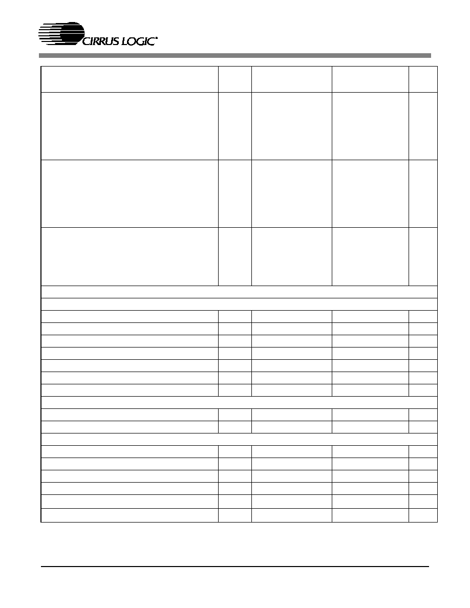
CS53L32A
6
DS513F1
Total Harmonic Distortion + Noise
(Note 1)
18 to 24-Bit
-1 dB
-20 dB
-60 dB
16-Bit
-1 dB
-20 dB
-60 dB
THD+N
-
-
-
-
-
-
-88
-73
-33
-86
-68
-28
-81
-
-
-
-
-
-
-
-
-
-
-
-85
-75
-35
-83
-65
-28
-78
-
-
-
-
-
dB
dB
dB
dB
dB
dB
Dynamic Range (PGA on)*
0 dB Gain
A-weighted
unweighted
12 dB Gain
A-weighted
unweighted
-
-
-
-
93
90
88
85
-
-
-
-
-
-
-
-
92
89
89
86
-
-
-
-
dB
dB
dB
dB
Total Harmonic Distortion + Noise (PGA on)*
(Note 1)
0 dB Gain
18 to 24-Bit -1 dB
12 dB Gain
18 to 24-Bit -1 dB
THD+N
-
-
78
73
-
-
-
-
77
76
-
-
dB
dB
* PGA = Programmable Gain Amplifier
CS53L32A-BZ Analog Input Characteristics for VA=1.8 - 3.3V
Interchannel Isolation
1 kHz
-
90
-
-
90
-
dB
Interchannel Gain Mismatch
-
0.1
-
-
0.1
-
dB
Offset Error with High Pass Filter
-
-
0
-
-
0
LSB
Full Scale Input Voltage
-7%
VA/3.6
+7%
-7%
VA/3.6 +7%
Vrms
Gain Drift
-
100
-
-
100
-
ppm/�C
Input Resistance
10
-
-
10
-
-
k
Input Capacitance
-
-
15
-
-
15
pF
Programmable Gain Characteristics
Gain Step Size
-
1.0
-
-
1.0
-
dB
Absolute Gain Step Error
-
-
0.3
-
-
0.3
dB
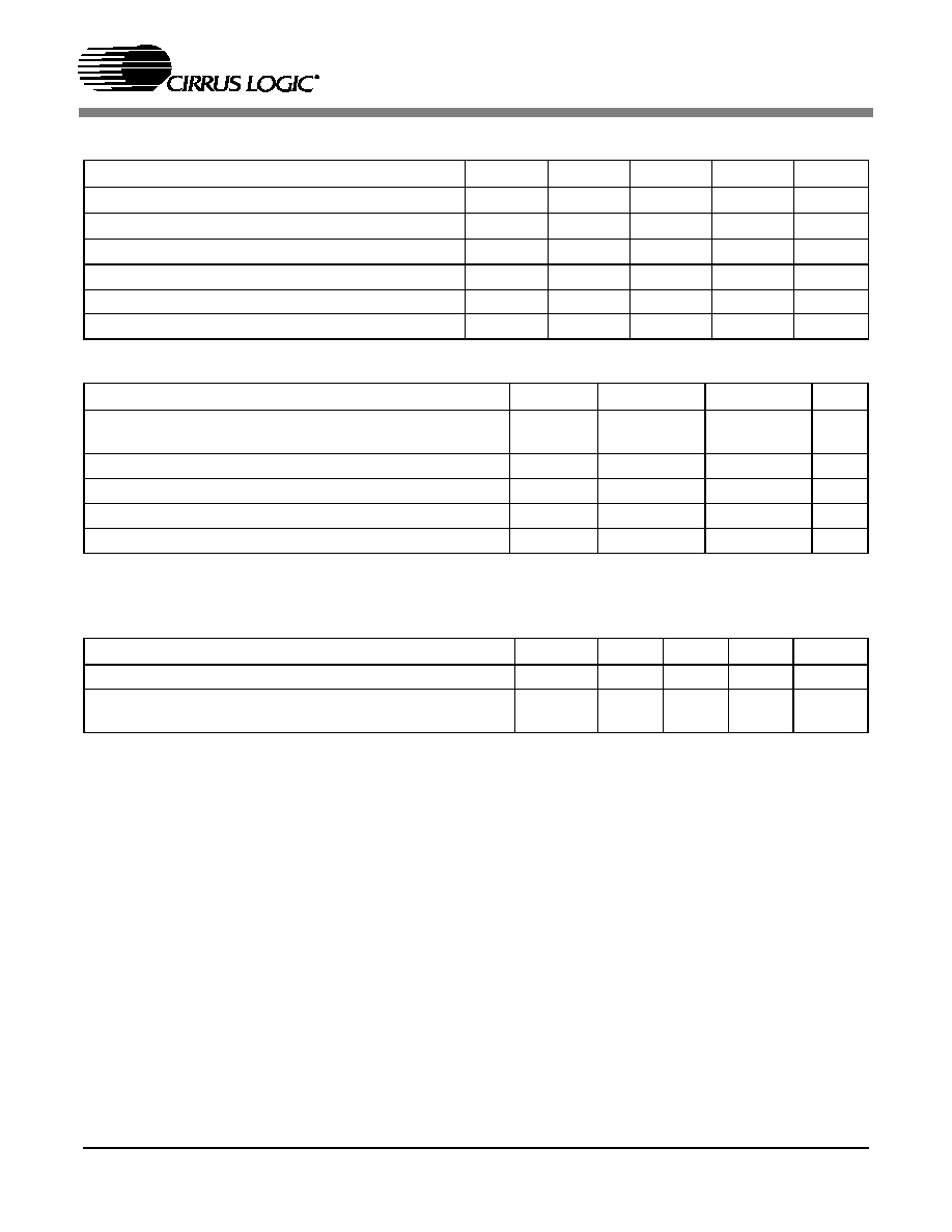
A/D Decimation Filter Characteristics
(Note 2)
Passband
(Note 3)
0
-
23.5
0
-
47.5
kHz
Passband Ripple
-0.08
-
+0.17 -0.09
-
0
dB
Stopband
(Note 3)
27.5
-
-
64.1
-
-
kHz
Stopband Attenuation
(Note 4)
-60.3
-
-
-48.4
-
-
dB
Group Delay (Fs = Output Sample Rate)
(Note 5)
t
gd
-
10/Fs
-
-
2.7/Fs
-
s
Group Delay Variation vs. Frequency
t
gd
-
-
0.03
-
-
0.007
�s
Parameter
Symbol
Base-rate Mode
High-rate Mode
Unit
Min
Typ
Max
Min
Typ
Max

CS53L32A
DS513F1
7
Notes: 1. Referenced to typical full-scale input voltage (0.5 Vrms).
2. Filter response is not tested but is guaranteed by design.
3. Filter characteristics scale with output sample rate. For output sample rates, Fs, other than 48 kHz, the
0.01 dB passband edge is 0.4535x Fs and the stopband edge is 0.625x Fs.
4. The analog modulator samples the input at 6.144 MHz for an Fs equal to 48 kHz. There is no rejection
of input signals which are multiples of the sampling frequency (n x 6.144 MHz �21.8 kHz where
n = 0,1,2,3...).
5. Group delay for Fs = 48 kHz, t
gd
= 10/48 kHz = 208 �s.
High Pass Filter Characteristics
Frequency Response
-3 dB
(Note 2)
-0.1 dB
-
-
3.7
24.2
-
-
-
-
3.7
24.2
-
-
Hz
Hz
Phase Deviation
@ 20 Hz
(Note 2)
-
10
-
-
10
-
Degree
Passband Ripple (Note 2)
-
-
0.17
-
-
0.09
dB
Parameter
Symbol
Base-rate Mode
High-rate Mode
Unit
Min
Typ
Max
Min
Typ
Max

CS53L32A
8
DS513F1
POWER AND THERMAL CHARACTERISTICS
Notes: 6. Power Down Mode is defined as the chip being held in reset with MCLK running. To lower power
consumption further, remove MCLK.
7. Valid with the recommended capacitor values on FILT+ and VQ as shown in Figure 6.
Base-Rate Mode
High-Rate Mode
Parameters
Symbol
Min
Typ
Max
Min
Typ
Max
Units
Power Supplies
Power Supply Current-
VA=1.8 V
Normal Operation
VL=1.8 V
I
A
I
D_IO
-
-
6.0
150
-
-
-
-
7.6
300
-
-
mA
�A
Power Supply Current-
VA=1.8 V
Power Down Mode (Note 6)
VL=1.8 V
I
A
I
D_IO
-
-
100
0
-
-
-
-
250
0
-
-
�A
�A
Power Supply Current-
VA=3.0 V
Normal Operation
VL=3.0 V
I
A
I
D_IO
-
-
9
260
-
-
-
-
11.5
520
-
-
mA
�A
Power Supply Current-
VA=3.0 V
Power Down Mode
VL=3.0 V
I
A
I
D_IO
-
-
250
0
-
-
-
-
500
0
-
-
�A
�A
Total Power Dissipation-
All Supplies=1.8 V
Normal Operation
All Supplies=3.0 V
-
-
11
28
12
31
-
-
14.5
36
16
40
mW
mW
Package Thermal Resistance
JA
-
75
-
-
75
-
�C/Watt
Power Supply Rejection Ratio (1 kHz)
(Note 7)
(60 Hz)
PSRR
-
-
60
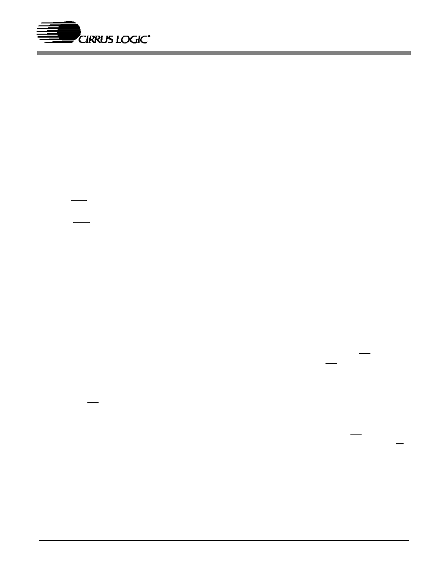
40
-
-
-
-
60
40
-
-
dB
dB
CS53L32A
DS513F1
9
DIGITAL CHARACTERISTICS
(T
A
= 25� C; VL = 1.7 V - 3.6 V; GND = 0 V)
ABSOLUTE MAXIMUM RATINGS
(GND = 0 V; all voltages with respect to ground.)
WARNING: Operation at or beyond these limits may result in permanent damage to the device. Normal operation is
not guaranteed at these extremes.
RECOMMENDED OPERATING CONDITIONS
(GND = 0V; all voltages with respect to ground.)
Parameters
Symbol Min
Typ
Max
Units
High-Level Input Voltage
V
IH
0.7�VL
-
-
V
Low-Level Input Voltage
V
IL
-
-
0.3�VL
V
High-Level Output Voltage
V
OH
0.7�VL
-
-
V
Low-Level Output Voltage
V
OL
-
-
0.3�VL
V
Leakage Current
I
in
-
-
�10
�A
Input Capacitance
-
8
-
pF
Parameters
Symbol
Min
Max
Units
DC Power Supplies:
Positive Analog
Digital I/O
VA
VL
-0.3
-0.3
4.0
4.0
V
V
Input Current, Any Pin Except Supplies
I
in
-
�10
mA
Digital Input Voltage
V
IND
-0.3
VL+0.4
V
Ambient Operating Temperature (power applied)
T
A
-55
125
�C
Storage Temperature
T
stg
-65
150
�C
Parameters
Symbol Min Typ
Max
Units
Ambient Temperature
T
A
-10
-
70
�C
DC Power Supplies:
Positive Analog
Digital I/O
VA
VL
1.7
1.7
-
-
3.6
3.6
V
V
CS53L32A
10
DS513F1
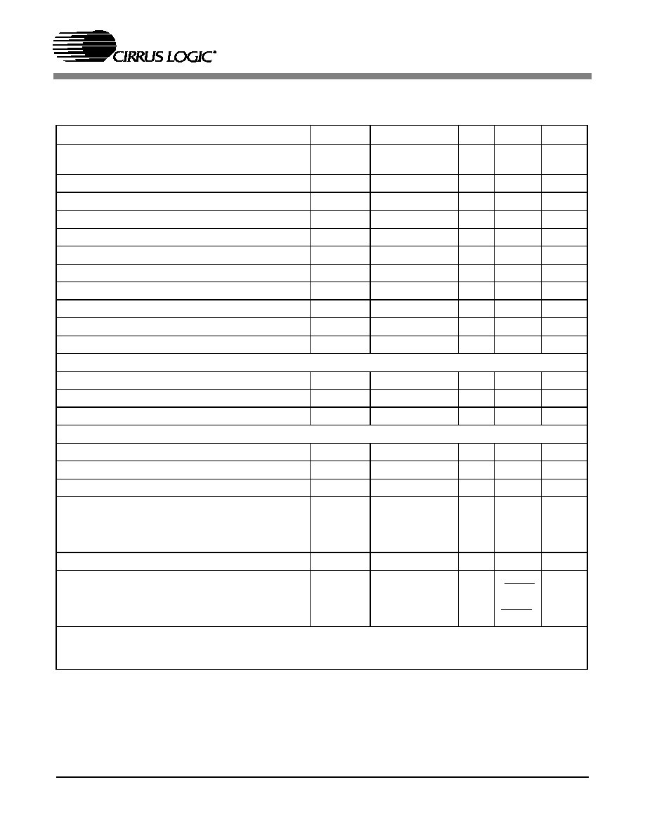
SWITCHING CHARACTERISTICS
(T
A
= -10 to 70� C; VA = 1.7 V - 3.6 V; Inputs: Logic 0 = GND,
Logic 1 = VL, C
L
= 20 pF)
8. There must be exactly 32, 48, 64, or 128 SCLK periods per LRCK transition.
9. Slave Mode operation requires an exact 50% duty cycle. Otherwise the CS53L32A will produce
erroneous data.
Parameters
Symbol Min Typ
Max
Units
Input Sample Rate
Base Rate Mode
High Rate Mode
Fs
Fs
2
50
-
-
50
100
kHz
kHz
MCLK Pulse Width High
MCLK/LRCK = 1024
8
-
-
ns
MCLK Pulse Width Low
MCLK/LRCK = 1024
8
-
-
ns
MCLK Pulse Width High
MCLK/LRCK = 768
10
-
-
ns
MCLK Pulse Width Low
MCLK/LRCK = 768
10
-
-
ns
MCLK Pulse Width High
MCLK/LRCK = 512
15
-
-
ns
MCLK Pulse Width Low
MCLK/LRCK = 512
15
-
-
ns
MCLK Pulse Width High MCLK / LRCK = 384 or 192
21
-
-
ns
MCLK Pulse Width Low MCLK / LRCK = 384 or 192
21
-
-
ns
MCLK Pulse Width High MCLK / LRCK = 256 or 128
31
-
-
ns
MCLK Pulse Width Low MCLK / LRCK = 256 or 128
31
-
-
ns
Master Mode
SCLK Falling to LRCK Edge
t
slrd
-20
-
20
ns
SCLK Falling to SDOUT Valid
t
sdo
0
-
20
ns
SCLK Duty Cycle
40
50
60
%
Slave Mode
LRCK Duty Cycle Notes 8, 9
-
50
-
%
Rise Time of Both LRCK and SCLK
t
r
-
-
10
ns
Fall Time of Both LRCK and SCLK
t
f
-
-
10
ns
SCLK Period
Base Rate Mode
High Rate Mode
t
sclkw
t
sclkw
-
-
-
-
ns
ns
SCLK Falling to LRCK Edge
t
slrd
-20
-
20
ns
SCLK Falling to SDOUT Valid
Base Rate Mode
High Rate Mode
t
dss
t
dss
-
-
-
-
ns
ns
NOTE: When operating the CS53L32A Revision C in Slave Mode, Base Rate Mode, certain timing requirements
must be met in addition to those specified above. The required timing relationship between the MCLK and LRCK
is shown in Figures 3. An MCLK rising edge cannot lead an LRCK transition by 6ns to 10ns.
1
128
(
)Fs
----------------------
1
64
( )Fs
------------------
1
(512)Fs
1
(256)Fs

CS53L32A
DS513F1
11
SCLK
LRCK
SDOUT
t
sclkl
t
slrd
t
dss
MSB
t
sclkh
t
sclkw
Figure 1. SCLK to LRCK and SDOUT, Slave Mode
SCLK
LRCK
SDOUT
t
slrd
t
sdo
MSB
MSB-1
Figure 2. SCLK to LRCK and SDOUT, Master Mode
LRCK Input
6 ns
10 ns
No rising edge of MCLK allowed within this
timing window.
MCLK Input
Figure 3. Relationship Required Between LRCK and MCLK in Slave Mode

CS53L32A
12
DS513F1
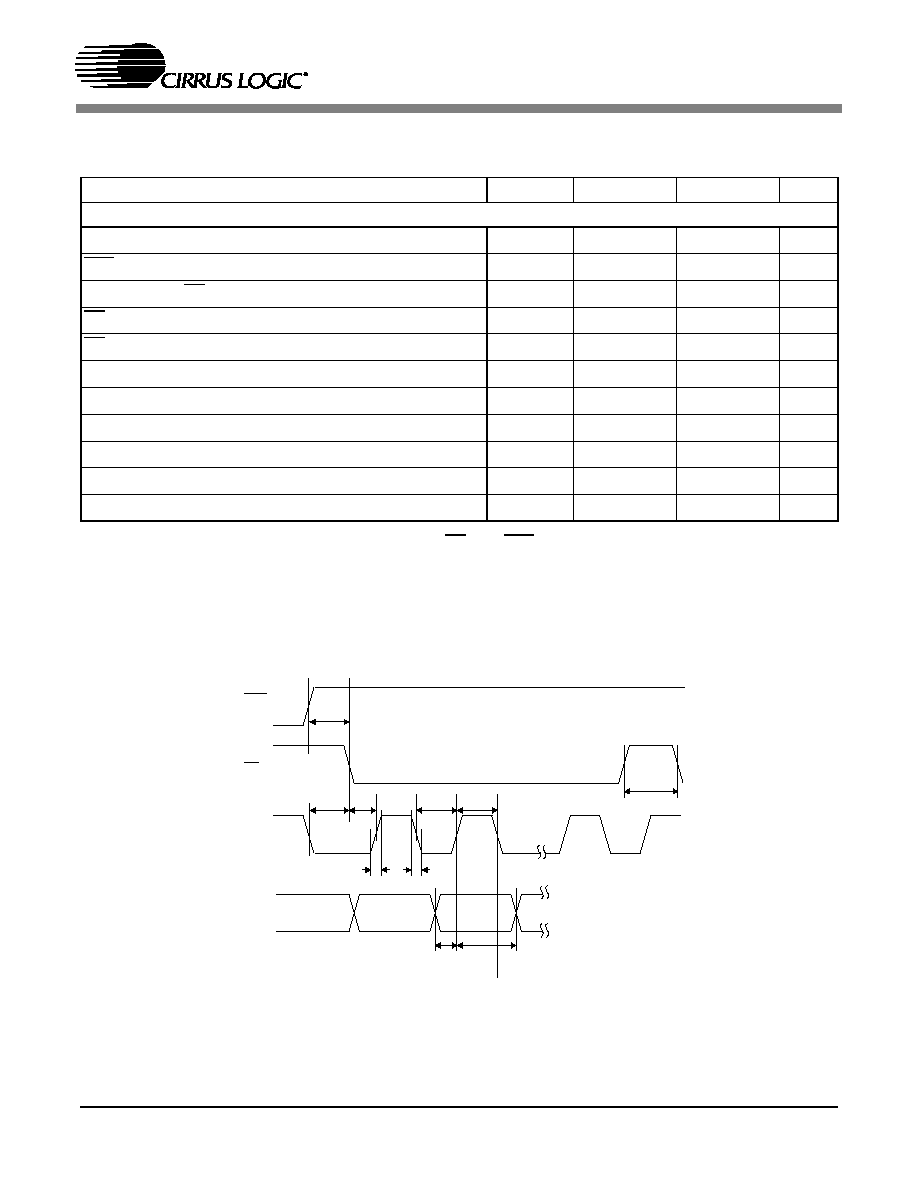
SWITCHING CHARACTERISTICS - CONTROL PORT - TWO WIRE MODE
(T
A
= 25� C; VL = 1.7 V - 3.6 V; Inputs: logic 0 = GND, logic 1 = VL, C
L
= 30 pF)
Note: 10. Data must be held for sufficient time to bridge the transition time, t
f
, of SCL
.
Parameter
Symbol
Min
Max
Unit
Two Wire Mode
SCL Clock Frequency
f
scl
-
100
KHz
RST Rising Edge to Start
t
irs
500
-
ns
Bus Free Time Between Transmissions
t
buf
4.7
-
�s
Start Condition Hold Time (prior to first clock pulse)
t
hdst
4.0
-
�s
Clock Low time
t
low
4.7
-
�s
Clock High Time
t
high
4.0
-
�s
Setup Time for Repeated Start Condition
t
sust
4.7
-
�s
SDA Hold Time from SCL Falling
(Note 10)
t
hdd
0
-
�s
SDA Setup time to SCL Rising
t
sud
250
-
ns
Rise Time of SCL
t
rc
-
25
ns
Fall Time of SCL
t
fc
-
25
ns
Rise Time of SDA
t
rd
-
1
us
Fall Time of SDA
t
fd
-
300
ns
Setup Time for Stop Condition
t
susp
4.7
-
�s
t
buf
t
hdst
t
hdst
t
low
t r
t f
t
hdd
t high
t sud
t sust
t susp
Stop
Start
Start
Stop
Repeated
SDA
SCL
t
irs
RST
Figure 4. Control Port Timing - Two Wire Mode
t
buf
t
hdst
t
hdst
t
low
t r
t f
t
hdd
t high
t sud
t sust
t susp
Stop
Start
Start
Stop
Repeated
SDA
SCL
t
irs
RST
CS53L32A
DS513F1
13
SWITCHING CHARACTERISTICS - CONTROL PORT - SPI MODE
(T
A
= 25 �C; VL = 1.7V - 3.6V; Inputs: logic 0 = GND, logic 1 = VL, C
L
= 30 pF)
Notes: 11. t
spi
only needed before first falling edge of CS after RST rising edge. t
spi
= 0 at all other times.
12. Data must be held for sufficient time to bridge the transition time of CCLK.
13. For F
SCLK
< 1 MHz.
Parameter
Symbol
Min
Max
Unit
SPI Mode
CCLK Clock Frequency
f
sclk
-
6
MHz
RST Rising Edge to CS Falling
t
srs
500
-
ns
CCLK Edge to CS Falling
(Note 11)
t
spi
500
-
ns
CS High Time Between Transmissions
t
csh
1.0
-
�s
CS Falling to CCLK Edge
t
css
20
-
ns
CCLK Low Time
t
scl
66
-
ns
CCLK High Time
t
sch
66
-
ns
CDIN to CCLK Rising Setup Time
t
dsu
40
-
ns
CCLK Rising to DATA Hold Time
(Note 12)
t
dh
15
-
ns
Rise Time of CCLK and CDIN
(Note 13)
t
r2
-
100
ns
Fall Time of CCLK and CDIN
(Note 13)
t
f2
-
100
ns
t r2
t f2
t dsu t dh
t sch
t scl
CS
CCLK
CDIN
t css
t csh
t spi
t srs
RST
Figure 5. Control Port Timing - SPI Mode
CS53L32A
14
DS513F1
2.
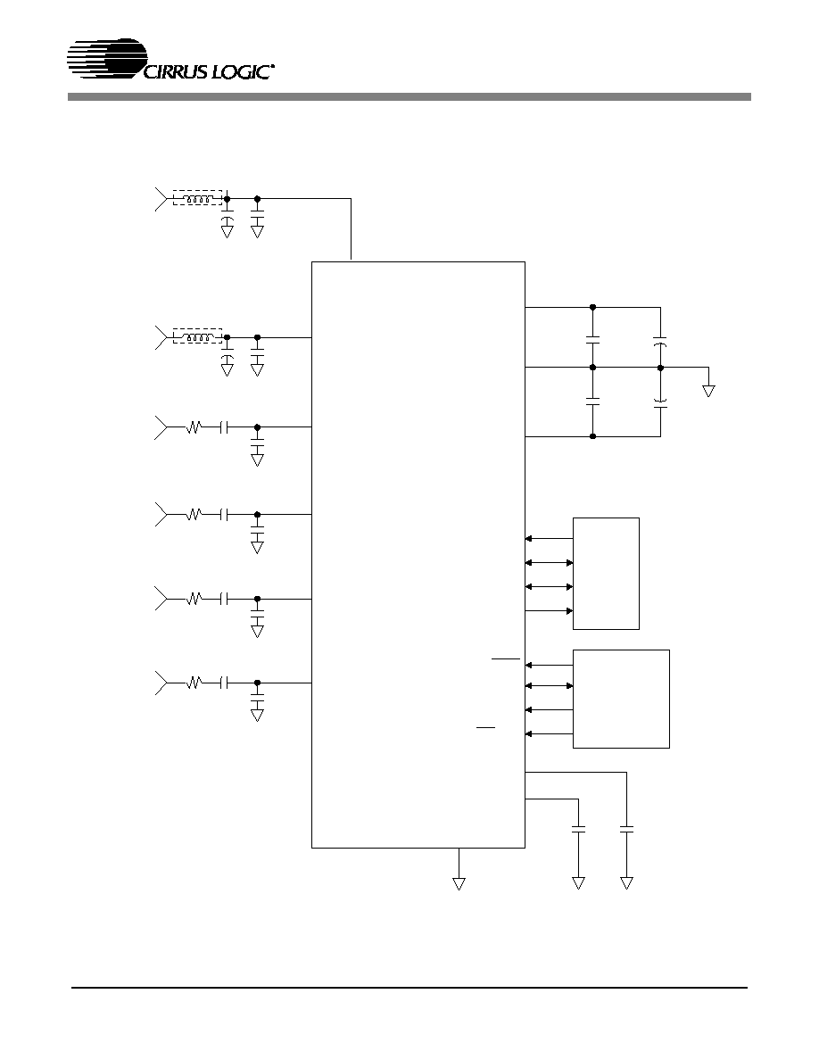
TYPICAL CONNECTION DIAGRAM
MCLK
LRCK
SCLK
RST
SDA/CDIN/DIF
SCL/CCLK/ChSEL
AD0/CS/DIV
GND
�c/
Digital
Audio
Source
VA
FILT+
REF_GND
CS53L32A
1.8 to 3.3 V
Supply
*Ferrite
bead
1.0 �F
0.1 �F
+
1.0 �F
1.8 to 3.3 V
Supply
1.0 �F
+
VL
*Ferrite
bead
+
5
1
13
16
6
Mode
Configuration
0.47 �F
150
0.47 �F
150
0.47 �F
150
0.01 �F
0.47 �F
150
AIN_L1
AIN_R1
AIN_L2
AIN_R2
**
**
**
**
SDOUT
**Optional if analog input
circuit is biased within
�5% of CS53L32A
nominal bias voltage
* Optional
VQ
1.0 �F
19
18
17
15
14
AFLTL
2
7
3
4
20
9
10
8
12
AFLTR
11
0.01 �F
0.01 �F
0.01 �F
0.1 �F
1 nF
1 nF
+
0.1 �F
0.1 �F
Figure 6. Typical Connection Diagram
CS53L32A
DS513F1
15
3.
REGISTER QUICK REFERENCE
** "default" ==> bit status after power-up-sequence or reset.
3.1
I/O and Power Control (address 01h)
BOOST
20 dB Digital Gain
Default = `0'
0 - Disabled
1 - Enabled
AINMUX Analog
Input
Multiplexer
Default ='0'.
0 - AIN_L1/AIN_R1 direct to A/D (default)
1 - AIN_L2/AIN_R2 direct to A/D
2 - AIN_L2/AIN_R2 through PGA to A/D
3 - Reserved
PDN Power-Down
Default ='1'.
0 - Disabled
1 - Enabled
CP_EN
Control Port Enable
Default ='0'.
0 - Disabled
1 - Enabled
3.2
Interface Control (address 02h)
MCLKDIV Master
Clock
Divider
Default ='0'.
0 - Disabled
1 - Enabled
RATIO1-0
Master Clock Ratio
Default ='0'.
0 - 128x (default)
1 - 192x
2 - 256x
3 - 384x
MASTER Master
Mode
Default ='0'.
0 - Slave Mode
1 - Master Mode
7
6
5
4
3
2
1
0
RESERVED
BOOST
AINMUX1
AINMUX0
RESERVED
RESERVED
PDN
CP_EN
0
0
0
0
0
0
1
0
7
6
5
4
3
2
1
0
RESERVED
MCLKDIV
RATIO1
RATIO0
MASTER
DIF2
DIF1
DIF0
0
0
0
0
0
0
0
0

CS53L32A
16
DS513F1
DIF2-0
Digital Interface Format
Default = `0'.
0 - I
2
S, up to 24-bit Data, Data valid on positive edge of SLCK (default)
1 - Left Justified, up to 24-bit Data, Data valid on positive edge of SLCK
2 - Reserved
3 - Right Justified, 16-bit Data, Data valid on positive edge of SLCK
4 - Right Justified, 24-bit Data, Data valid on positive edge of SLCK
5 - Right Justified, 18-bit Data, Data valid on positive edge of SLCK
6 - Right Justified, 20-bit Data, Data valid on positive edge of SLCK
7 - Reserved
3.3
Analog I/O Control (address 03h)
MUTEL Left
Channel
Mute
Default = `0'.
0 - Disabled
1 - Enabled
MUTER Right
Channel
Mute
Default = `0'.
0 - Disabled
1 - Enabled
SOFT
Soft Digital/Analog Volume Control
Default = `1'.
0 - Disabled
1 - Enabled
ZC
Analog Zero Cross Detection Control
Default = `1'.
0 - Disabled
1 - Enabled
INDVC
Independent Volume Control Enable
Default = `0'.
0 - Disabled
1 - Enabled
L=R
Left Channel Volume = Right Channel Volume
Default = `0'.
0 - Left channel volume is determined by the left channel volume control registers and right
channel volume is determined by the right channel volume control registers.
1 - Left and right channel volumes are determined by the left channel volume control registers
and the right channel volume control registers are ignored.
HPFREEZE
High-pass filter freeze
Default = `0'.
0 - Disabled
1 - Enabled
7
6
5
4
3
2
1
0
MUTEL
MUTER
SOFT
ZC
RESERVED
INDVC
L=R
HPFREEZE
0
0
1
1
0
0
0
0
CS53L32A
DS513F1
17
3.4
Left Channel Digital Volume Control (address 04h)
3.5
Right Channel Digital Volume Control (address 05h)
VOL7-0
Volume
Default = `0'.
(Refer to Table 13)
3.6
Analog Gain Control (address 06h)
LVOL3-0
Left Analog Gain
Default = `0'.
(Refer to Table 14)
RVOL3-0
Right Analog Gain
Default = `0'.
(Refer to Table 14)
3.7
Clip Detection Status (address 07h)
CLIP_L_FLAG
Left Channel Clip Detection
CLIP_R_FLAG
Right Channel Clip Detection
Default = `0'.
0 - No Clipping Detected
1 - Clipping Detected
7
6
5
4
3
2
1
0
VOL7
VOL6
VOL5
VOL4
VOL3
VOL2
VOL1
VOL0
0
0
0
0
0
0
0
0
7
6
5
4
3
2
1
0
LVOL3
LVOL2
LVOL1
LVOL0
RVOL3
RVOL2
RVOL1
RVOL0
0
0
0
0
0
0
0
0
7
6
5
4
3
2
1
0
RESERVED
RESERVED
RESERVED
RESERVED
RESERVED
RESERVED
CLIP_L_FLAG CLIP_R_FLAG
0
0
0
0
0
0
0
0

CS53L32A
18
DS513F1
4.
REGISTER DESCRIPTION
4.1
GAIN ENABLE
I/O and Power Control Register (address 01h)
Access:
R/W in Two Wire Mode and write only in SPI.
Default:
0 - Disabled
Function:
Applies a 20 dB digital gain to the input signal, regardless of the input path.
4.2
ANALOG INPUT MULTIPLEXER
I/O and Power Control Register (address 01h)
Access:
R/W in Two Wire Mode and write only in SPI.
Default:
0 - AIN_L1/AIN_R1 direct to A/D
Function:
The analog input multiplexer selects the input channel as well as the input path associated with vari-
ous gain stages.
7
6
5
4
3
2
1
0
RESERVED
BOOST
AINMUX1
AINMUX0
RESERVED
RESERVED
PDN
CP_EN
7
6
5
4
3
2
1
0
RESERVED
BOOST
AINMUX1
AINMUX0
RESERVED
RESERVED
PDN
CP_EN
AINMUX
MODE
0
AIN_L1/AIN_R1 direct to A/D
1
AIN_L2/AIN_R2 direct to A/D
2
AIN_L2/AIN_R2 through PGA to A/D
3
Reserved
Table 1. Analog Input Options
CS53L32A
DS513F1
19
4.3
POWER-DOWN
I/O and Power Control Register (address 01h)
Access:
R/W in Two Wire Mode and write only in SPI.
Default:
1 - Enabled
Function:
The entire device will enter a low-power state whenever this function is activated. The power-down
bit defaults to `enabled' on power-up and must be disabled before normal operation will begin. The
contents of the control registers are retained when this mode is enabled.
4.4
CONTROL PORT ENABLE
I/O and Power Control Register (address 01h)
Access:
R/W in Two Wire Mode and write only in SPI.
Default:
0 - Disabled
Function:
The CS53L32A will enter Control Port mode when this bit is enabled. Stand-Alone is the default power
up mode. See Section 6.3,
Recommended Power-up Sequence,
for more details.
7
6
5
4
3
2
1
0
RESERVED
BOOST
AINMUX1
AINMUX0
RESERVED
RESERVED
PDN
CP_EN
PDN
MODE
0
Disabled
1
Enabled
Table 2. Power-Down Enable
7
6
5
4
3
2
1
0
RESERVED
BOOST
AINMUX1
AINMUX0
RESERVED
RESERVED
PDN
CP_EN
CP_EN
MODE
0
Disabled
1
Enabled
Table 3. Control Port Enable
CS53L32A
20
DS513F1
4.5
MASTER CLOCK DIVIDE
Interface Control Register (address 02h)
Access:
R/W in Two Wire Mode and write only in SPI.
Default:
0 - Disabled
Function:
Divides MCLK by two prior to all other chip circuitry.
4.6
MASTER CLOCK RATIO
Interface Control Register (address 02h)
Access:
R/W in Two Wire Mode and write only in SPI.
Default:
0 - 128x
Function:
Sets the ratio of MCLK to LRCK.
7
6
5
4
3
2
1
0
RESERVED
MCLKDIV
RATIO1
RATIO0
MASTER
DIF2
DIF1
DIF0
MCLKDIV
MODE
0
Disabled
1
Enabled
Table 4. Master Clock Divide Select
7
6
5
4
3
2
1
0
RESERVED
MCLKDIV
RATIO1
RATIO0
MASTER
DIF2
DIF1
DIF0
RATIO1,0
MCLK/LRCK RATIO (MCLKDIV=0)
MCLK/LRCK RATIO (MCLKDIV=1)
0
128x
256x
1
192x
384x
2
256x
512x
3
384x
768x
Table 5. MCLK/LRCK Ratios
CS53L32A
DS513F1
21
4.7
MASTER MODE
Interface Control Register (address 02h)
Access:
R/W in Two Wire Mode and write only in SPI.
Default:
0 - Slave Mode
Function:
Configures the device for master or slave operation when in Control Port mode.
4.8
DIGITAL INTERFACE FORMAT
Interface Control Register (address 02h)
Access:
R/W in Two Wire Mode and write only in SPI.
Default:
0 - Format 0 (I
2
S, up to 24-bit data, Data valid on positive edge of SCLK)
Function:
The required relationship between the Left/Right clock, serial clock and serial data is defined by the
Digital Interface Format and the options are detailed in Figures 18 through 21.
7
6
5
4
3
2
1
0
RESERVED
MCLKDIV
RATIO1
RATIO0
MASTER
DIF2
DIF1
DIF0
MASTER
MODE
0
Slave Mode
1
Master Mode
Table 6. Master/Slave Mode Selection
7
6
5
4
3
2
1
0
RESERVED
MCLKDIV
RATIO1
RATIO0
MASTER
DIF2
DIF1
DIF0
DIF2 DIF1 DIF0
DESCRIPTION
Format
FIGURE
0
0
0
I
2
S, up to 24-bit Data, Data valid on positive edge of SCLK
0
18
0
0
1
Left Justified, up to 24-bit Data, Data valid on positive edge of SCLK
1
19
0
1
0
Reserved
2
-
0
1
1
Right Justified, 16-bit Data, Data valid on positive edge of SCLK
3
18
1
0
0
Right Justified, 24-bit Data, Data valid on positive edge of SCLK
4
19
1
0
1
Right Justified, 18-bit Data, Data valid on positive edge of SCLK
5
20
1
1
0
Right Justified, 20-bit Data, Data valid on positive edge of SCLK
6
21
1
1
1
Reserved
7
-
Table 7. Digital Interface Format
CS53L32A
22
DS513F1
4.9
LEFT/RIGHT CHANNEL MUTE
Analog I/O Control (address 03h)
Access:
R/W in Two Wire Mode and write only in SPI.
Default:
0 - Disabled
Function:
Digital mute of the left and right channels.
4.10
SOFT RAMP AND ZERO CROSS ENABLE
Analog I/O Control Register (address 03h)
Access:
R/W in Two Wire Mode and write only in SPI.
Default:
11 - Soft Ramp and Zero Cross enabled
Function:
Soft Ramp Enable
Soft Ramp allows level changes, both muting and attenuation, to be implemented via an incremental
ramp. Digital volume control is ramped from the current level to the new level at a rate of 1/8 dB per
left/right clock period. Analog volume control is ramped in 1 dB steps every 8 left/right clock periods
in Base Rate mode, and 1 dB every 16 left/right clock periods in High Rate mode.
Zero Cross Enable
Zero Cross Enable dictates that signal level changes, either by attenuation changes or muting, will
occur on a signal zero crossing to minimize audible artifacts. The requested level change will occur
after a timeout period of 512 sample periods in BRM or 1024 sample periods in HRM (approximately
10.7 ms at 48 kHz sample rate) if the signal does not encounter a zero crossing. The zero cross func-
tion is independently monitored and implemented for each channel.
7
6
5
4
3
2
1
0
MUTEL
MUTER
SOFT
ZC
RESERVED
INDVC
L=R
HPFREEZE
MUTEL/
MUTER
MODE
0
Disabled
1
Enabled
Table 8. Left/Right Channel Mute Enable
7
6
5
4
3
2
1
0
MUTEL
MUTER
SOFT
ZC
RESERVED
INDVC
L=R
HPFREEZE
CS53L32A
DS513F1
23
Soft Ramp and Zero Cross Enable
Soft Ramp and Zero Cross Enable dictates that signal level changes, either by attenuation changes
or muting, will occur in 1 dB steps and be implemented on a signal zero crossing. The level change
will occur after a timeout period of 512 sample periods in BRM or 1024 sample periods in HRM (ap-
proximately 10.7 ms at 48 kHz sample rate) if the signal does not encounter a zero crossing. The zero
cross function is independently monitored and implemented for each channel.
.
4.11
INDEPENDENT VOLUME CONTROL ENABLE
Analog I/O Control Register (address 03h)
Access:
R/W in Two Wire Mode and write only in SPI.
Default:
0 - Enabled
Function:
When this function is disabled, the AIN_L and AIN_R volume levels are controlled by the Left and
Right Volume Control registers and the Independent Analog Gain Control registers are ignored.
When this function is enabled, the volume levels are determined by both the Volume Control registers
and the Independent Analog Gain Control registers.
SOFT/ZC
ANALOG VOLUME CONTROL MODES
00
Change volume immediately
01
Change volume at next zero cross time
10
Change volume in 1 dB steps
11
Change volume in 1 dB steps at every zero cross time
Table 9. Analog Volume Control
SOFT
DIGITAL VOLUME CONTROL MODES
0
Change volume immediately
1
Change volume in1/8 dB steps
Table 10. Digital Volume Control
7
6
5
4
3
2
1
0
MUTEL
MUTER
SOFT
ZC
RESERVED
INDVC
L=R
HPFREEZE
INDVC
MODE
0
Enabled
1
Frozen
Table 11. Independent Volume Control Enable
CS53L32A
24
DS513F1
4.12
LEFT CHANNEL VOLUME = RIGHT CHANNEL VOLUME
Analog I/O Control (address 03h)
Access:
R/W in Two Wire Mode and write only in SPI.
Default:
0 - Disabled
Function:
When this function is disabled, the left channel volume is determined by the left channel volume con-
trol register and right channel volume is determined by the right channel volume control register.
When enabled, the left and right channel volumes are determined by the left channel volume control
register and the right channel volume control register is ignored.
4.13
HIGH-PASS FILTER FREEZE
Analog I/O Control Register (address 03h)
Access:
R/W in Two Wire Mode and write only in SPI.
Default:
0 - Enabled
Function:
The high-pass filter works by continuously subtracting a measure of the dc offset from the output of
the decimation filter. If the HPFREEZE bit is taken low during normal operation, the current value of
the dc offset is frozen and this dc offset will continue to be subtracted from the conversion result. This
feature makes it possible to perform a system calibration by:
1) removing the signal source at the input to the subsystem containing the CS53L32A,
2) running the CS53L32A with the HPFREEZE bit high until the filter settles, approximately
one second,
3) taking the HPFREEZE bit low, thus disabling the high-pass filter and freezing the stored dc offset.
A system calibration performed in this way will eliminate offsets anywhere in the signal path between
the calibration point and the CS53L32A.
7
6
5
4
3
2
1
0
MUTEL
MUTER
SOFT
ZC
RESERVED
INDVC
L=R
HPFREEZE
7
6
5
4
3
2
1
0
MUTEL
MUTER
SOFT
ZC
RESERVED
INDVC
L=R
HPFREEZE
HPFREEZE
MODE
0
Enabled
1
Frozen
Table 12. High-Pass Filter Enable
CS53L32A
DS513F1
25
4.14
VOLUME CONTROL
Left Channel Volume Control Register (address 04h)
Right Channel Volume Control Register (address 05h)
Access:
R/W in Two Wire Mode and write only in SPI.
Default:
0 - 0 dB (No attenuation)
Function:
The Volume Control allows the user to alter the signal level in 1 dB increments from +12 to -96 dB, when
the INDVC bit is disabled. When INDVC is enabled, the Volume Control can be altered in 1 dB increments
from 0 to -96 dB. Volume settings are decoded as shown in Table 13, using a 2's complement code. The
volume changes are implemented as dictated by the Soft and Zero Cross bits in the Analog I/O Control
register. All volume settings less than -96 dB are equivalent to muting the channel.
7
6
5
4
3
2
1
0
VOL7
VOL6
VOL5
VOL4
VOL3
VOL2
VOL1
VOL0
Binary Code
Decimal Value
Volume Setting
00001010
12
+12 dB
00000111
7
+7 dB
00000000
0
0 dB
11000100
-60
-60 dB
10100110
-90
-90 dB
Table 13. Example Volume Settings
CS53L32A
26
DS513F1
4.15
LEFT/RIGHT ANALOG GAIN
ADC Independent Analog Gain Control Register (address 06h)
Access:
R/W in Two Wire Mode and write only in SPI.
Default:
0 - 0 dB (No Gain)
Function:
The level of the left and right analog channels can be adjusted in 1 dB increments as dictated by the
Soft Ramp and Zero Cross bits from 0 to +12 dB when routed through the PGA via the AINMUX bits
in Control Port mode or the CH_SEL pins in Stand-Alone mode. Levels are decoded as shown in
Table 14. Levels above +12 dB are interpreted as +12 dB.
4.16
CLIP DETECTION
Clip Detection Status Register (address 07h)
Access:
Read only in Two Wire Mode and unavailable in SPI.
Default:
0 - No Clipping Detected
Function:
The Clip Flags indicate when there is an over-range condition anywhere in the CS53L32A internal signal
path. These bits are "sticky". They constantly monitor the ADC signal path and are set to 1 when an over-
range condition occurs. They are reset to 0 when read.
7
6
5
4
3
2
1
0
LVOL3
LVOL2
LVOL1
LVOL0
RVOL3
RVOL2
RVOL1
RVOL0
Binary Code
Decimal Value
Volume Setting
0000
0
0 dB
0010
2
+2 dB
1010
6
+6 dB
1001
9
+9 dB
1100
12
+12 dB
Table 14. Example Gain Settings
7
6
5
4
3
2
1
0
RESERVED
RESERVED
RESERVED
RESERVED
RESERVED
RESERVED
CLIP_L_FLAG CLIP_R_FLAG
CLIP_L_FLAG
CLIP_R_FLAG
Condition
0
Signal within normal range
1
Signal is over-range
Table 15. Clip Detection Status Bits
CS53L32A
DS513F1
27
5.
PIN DESCRIPTION
Interface Power
VL
RST
Reset
Master Clock
MCLK
VQ
Quiescent Voltage
Serial Clock
SCLK
AIN_L1 Analog Input 1 Left
Serial Audio Data Out
SDOUT
AIN_R1
Analog Input 1 Right
Analog Power
VA
REF_GND
Reference Ground
Ground
GND
AIN_L2 Analog Input 2 Left
Left/Right Clock
LRCK
AIN_R2 Analog Input 2 Right
AD0/CS/DIV AD0/CS/DIV
FILT+
Positive Voltage Reference
SDA/CDIN/DIF SDA/CDIN/DIF
AFLTL
Anti-Aliasing Capacitor
SCL/CCLK/ChSEL SCL/CCLK/ChSEL
AFLTR Anti-Aliasing Capacitor
1
2
3
4
5
6
7
8
9
10
11
12
5
1
2
6
20
19
18
17
16
15
14
13
Interface Power
1
VL
(
Input) - Digital interface power supply. Typically 1.8 to 3.3 VDC.
Master Clock
2
MCLK
(
Input) - The master clock frequency must be either 256x, 384x,
512x, 768x or 1024x the input sample rate in Base Rate Mode (BRM) and
128x, 192x, 256x, 384x the input sample rate in High Rate Mode (HRM).
Table 16 illustrates several standard audio sample rates and the required
master clock frequencies.
Serial Clock
3
SCLK
(
Input/Output) - Clocks the individual bits of the serial data out of the
SDOUT pin. The required relationship between the Left/Right clock, serial
clock and serial data is defined by the DIF2-0 bytes when in Control Port
mode or by the DIF1-0 pins when in Stand-Alone mode.
Serial Audio Data Out
4
SDOUT
(
Output) - This pin serves two functions.
First: Two's complement MSB-first serial data is output on this pin. The data
is clocked out of SDOUT via the serial clock and the channel is determined
by the Left/Right clock. The required relationship between the Left/Right
clock, serial clock and serial data is defined by the DIF2-0 bytes when in
Control Port mode or by the DIF pin when in Stand-Alone mode.
Second: In Stand-alone mode, Master/Slave mode selection is determined,
at start-up, by a 47 kOhm pull-up/pull-down on this line. A pull-up to VL
selects Master mode and a pull-down to GND selects Slave mode.
Analog Power
5
VA
(
Input) - Analog power supply. Typically 1.8 to 3.3 VDC.
Ground
6
GND
(
Input) - Ground Reference.
Left/Right Clock
7
LRCK
(
Input/Output) - The Left/Right clock determines which channel is cur-
rently being output on the serial audio data line SDOUT. The frequency of
the Left/Right clock must be at the input sample rate. The required relation-
ship between the Left/Right clock, serial clock and serial data is defined by
the DIF2-0 bytes when in Control Port mode or by the DIF pin when in
Stand-Alone mode.
CS53L32A
28
DS513F1
Address Bit
8
AD0/CS (Control Port Mode)
(
Input) - In Two Wire mode, AD0 is a chip
address bit. CS is used to enable the control port interface in SPI mode.
MCLK Divide Enable
8
DIV (Stand-Alone Mode)
(
Input) - When high, the chip will enter High Rate
Mode. When this pin is low, the chip will enter Base Rate Mode.
Serial Control Data I/O
9
SDA/CDIN (Control Port Mode)
(
Input/Output) - In Two Wire mode, SDA is
a data I/O line. CDIN is the input data line for the control port interface in SPI
mode.
Digital Interface Format
9
DIF (Stand-Alone Mode)
(
Input) - The required relationship between the
Left/Right clock, serial clock and serial data is defined by the Digital Interface
Format.
Serial Control
Interface Clock
10
SCL/CCLK (Control Port Mode)
(
Input) - Clocks the serial control data into
or from SDA/CDIN/DIF.
Channel Select
10
ChSEL (Stand-Alone Mode)
(
Input) - The analog data path is determined
by the Channel Select bit. These options are detailed in Table 18.
Anti-Aliasing Capacitors
11, 12
AFLTR, AFLTL
(
Output) - Anti-aliasing capacitors for the left and right chan-
nels. An external capacitor is required from AFLTR and AFLTL to ground, as
shown in Figure 5. AFLTR and AFLTL are not intended to supply external
current, and any current drawn from these pins will alter device perfor-
mance.
Positive Voltage
Reference
13
FILT+
(
Output) - Positive reference for internal sampling circuits. An external
capacitor is required from FILT+ to ground, as shown in Figure 6. The rec-
ommended value will typically provide 60 dB of PSRR at 1 kHz and 40 dB of
PSRR at 60 Hz. FILT+ is not intended to supply external current. FILT+ has
a typical source impedance of 250 k
and any current drawn from this pin
will alter device performance.
Analog Inputs
14, 15, 17, and 18
AIN_R1, AIN_L1, AIN_R2, AIN_L2
(
Input) - Channel 1/Channel 2 analog
inputs.
Sample
Rate
(kHz)
MCLK (MHz)
HRM
BRM
128x
192x
256x*
384x*
256x
384x
512x
768x*
1024x*
32
4.0960
6.1440
8.1920
12.2880
8.1920
12.2880
16.3840
24.5760
32.7680
44.1
5.6448
8.4672
11.2896
16.9344
11.2896
16.9344
22.5792
32.7680
45.1584
48
6.1440
9.2160
12.2880
18.4320
12.2880
18.4320
24.5760
36.8640
49.1520
64
8.1920
12.2880
16.3840
24.5760
-
-
-
-
-
88.2
11.2896
16.9344
22.5792
33.8688
-
-
-
-
-
96
12.2880
18.4320
24.5760
36.8640
-
-
-
-
-
* MCLKDIV = 1 in Control Port mode or DIV= Hi when in Stand-Alone mode
Table 16. Common Clock Frequencies
DIF
DESCRIPTION
0
I
2
S, up to 24-bit data
1
Left Justified, up to 24-bit data
Table 17. Digital Interface Format - DIF (Stand-Alone Mode)
ChSEL
DESCRIPTION
0
Channel 1 directly to A/D
1
Channel 2 with 32dB of gain
Table 18. Channel Select Options
CS53L32A
DS513F1
29
Reference Ground
16
REF_GND
(
Input) - Ground reference for the internal sampling circuits. Must
be connected to ground.
Quiescent Voltage
19
VQ
(
Output) - Filter connection for internal A/D converter quiescent refer-
ence voltage. A capacitor must be connected from VQ to ground. VQ is not
intended to supply external current. VQ has a typical source impedance of
250 k
and any current drawn from this pin will alter device performance.
Reset
20
RST
(
Input) - The device enters a low power mode and all internal registers
are reset to their default settings, including the control port, when low. When
high, the control port becomes operational and the PDN bit must be cleared
before normal operation will occur. The control port cannot be accessed
when Reset is low.
CS53L32A
30
DS513F1
6. APPLICATIONS
6.1
GROUNDING AND POWER SUPPLY DECOUPLING
As with any high resolution converter, the CS53L32A requires careful attention to power supply and
grounding arrangements to optimize performance. Figure 6 shows the recommended power arrangement
with VA and VL connected to clean supplies. Decoupling capacitors should be located as close to the de-
vice package as possible.
6.2
OVERSAMPLING MODES
The CS53L32A operates in one of two oversampling modes. Base Rate Mode supports input sample
rates up to 50 kHz while High Rate Mode supports input sample rates up to 100 kHz. See Table 16 for
more details.
6.3
RECOMMENDED POWER-UP SEQUENCE
1) Hold RST low until the power supply, master, and left/right clocks are stable. In this state, the control
port is reset to its default settings and VQ will remain low.
2) Bring RST high. The device will remain in a low power state with VQ low and will initiate the Stand-
Alone power-up sequence. The control port will be accessible at this time. If control port operation is
desired, write the CP_EN bit prior to the completion of the Stand-Alone power-up sequence, approx-
imately 1024 LRCK cycles. Writing this bit will halt the Stand-Alone power-up sequence and initialize
the control port to its default settings. The desired register settings can be loaded while keeping the
PDN bit set to 1.
3) If Control Port mode is selected via the CP_EN bit, set the PDN bit to 0 which will initiate the power-
up sequence, which requires approximately 50 �S.
7. CONTROL PORT INTERFACE
The control port is used to load all the internal settings. The operation of the control port may be complete-
ly asynchronous with the audio sample rate. However, to avoid potential interference problems, the con-
trol port pins should remain static if no operation is required.
The control port has 2 modes: SPI and Two Wire. If Two Wire operation is desired, AD0/CS should be
tied to VL or GND. If the CS53L32A ever detects a high to low transition on AD0/CS after power-up, SPI
mode will be selected.
7.1
SPI MODE
In SPI mode, CS is the CS53L32A chip select signal, CCLK is the control port bit clock, CDIN is the input
data line from the microcontroller and the chip address is 0010000. All signals are inputs and data is
clocked in on the rising edge of CCLK. All CS53L32A registers are write-only in SPI mode.
Figure 7 shows the operation of the control port in SPI mode. To write to a register, bring CS low. The first
7 bits on CDIN form the chip address, and must be 0010000. The eighth bit is a read/write indicator (R/W),
which must be low to write. The next 8 bits form the Memory Address Pointer (MAP), which is set to the
address of the register that is to be updated. The next 8 bits are the data which will be placed into the
register designated by the MAP.
The CS53L32A has a MAP auto increment capability, enabled by the INCR bit in the MAP. If INCR is a
zero, then the MAP will stay constant for successive writes. If INCR is set to a 1, then MAP will auto in-
crement after each byte is written, allowing block writes of successive registers.

CS53L32A
DS513F1
31
7.2
TWO WIRE MODE
In Two Wire mode, SDA is a bidirectional data line. Data is clocked into and out of the part by the clock,
SCL, with the clock to data relationship as shown in Figure 8. There is no CS pin. Pin AD0 forms the partial
chip address and should be tied to VL or GND as required. The upper 6 bits of the 7 bit address field must
be 001000. To communicate with the CS53L32A the LSB of the chip address field, which is the first byte
sent to the CS53L32A, should match the setting of the AD0 pin. The eighth bit of the address byte is the
R/W bit (high for a read, low for a write). If the operation is a write, the next byte is the Memory Address
Pointer which selects the register to be read or written. See Section 7.3,
Memory Address Pointer (MAP).
If the operation is a read, the contents of the register pointed to by the Memory Address Pointer will be
output. Setting the auto increment bit in MAP, allows successive reads or writes of consecutive registers.
Each byte is separated by an acknowledge bit.
Note: The Two-Wire control port mode is compatible with the I
2
C protocol.
7.3
MEMORY ADDRESS POINTER (MAP)
INCR (Auto MAP Increment Enable)
Default = `0'.
0 - Disabled
1 - Enabled
MAP0-2 (Memory Address Pointer)
Default = `000'.
7
6
5
4
3
2
1
0
INCR
Reserved
Reserved
Reserved
Reserved
MAP2
MAP1
MAP0
0
0
0
0
0
0
0
0
CS53L32A
32
DS513F1
MAP
MSB
LSB
DATA
byte 1
byte n
R/W
MAP = Memory Address Pointer
ADDRESS
CHIP
CDIN
CCLK
CS
0010000
Figure 7. Control Port Timing, SPI Mode
SDA
SCL
001000
ADDR
AD0
R/W
Start
ACK
DATA
1-8
ACK
DATA
1-8
ACK
Stop
Note: If operation is a write, this byte contains the Memory Address Pointer, MAP.
Note 1
Figure 8. Control Port Timing, Two Wire Mode
CS53L32A
DS513F1
33
-100
-90
-80
-70
-60
-50
-40
-30
-20
-10
0
0
0.1
0.2
0.3
0.4
0.5
0.6
0.7
0.8
0.9
1
Frequency (normalized to Fs)
A
m
pl
i
t
ude
dB
-100
-90
-80
-70
-60
-50
-40
-30
-20
-10
0
0.4
0.42
0.44
0.46
0.48
0.5
0.52
0.54
0.56
0.58
0.6
Frequency (normalized to Fs)
A
m
pl
i
t
ude
dB
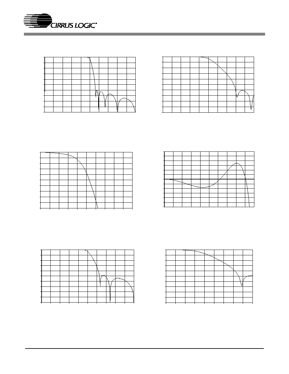
Figure 9. Base-Rate Stopband Rejection
Figure 10. Base-Rate Transition Band
-0.3
-0.25
-0.2
-0.15
-0.1
-0.05
0
0.05
0.1
0.15
0.2
0.25
0.3
0
0.05
0.1
0.15
0.2
0.25
0.3
0.35
0.4
0.45
0.5
Frequency (normalized to Fs)
A
m
pl
i
t
ude
dB
Figure 11. Base-Rate Transition Band (Detail)
Figure 12. Base-Rate Passband Ripple
-10
-9
-8
-7
-6
-5
-4
-3
-2
-1
0
0.45
0.46
0.47
0.48
0.49
0.5
0.51
0.52
0.53
0.54
0.55
Frequency (normalized to Fs)
A
m
pl
i
t
ude
dB
-100
-90
-80
-70
-60
-50
-40
-30
-20
-10
0
0
0.1
0.2
0.3
0.4
0.5
0.6
0.7
0.8
0.9
1
Frequency (normalized to Fs)
A
m
pl
i
t
ude
dB
-100
-90
-80
-70
-60
-50
-40
-30
-20
-10
0
0.4
0.43
0.46
0.49
0.52
0.55
0.58
0.61
0.64
0.67
Frequency (normalized to Fs)
A
m
pl
i
t
ude
dB
Figure 13. High-Rate Stopband Rejection
Figure 14. High-Rate Transition Band
CS53L32A
34
DS513F1
-10
-9
-8
-7
-6
-5
-4
-3
-2
-1
0
0.45
0.46
0.47
0.48
0.49
0.5
0.51
0.52
0.53
0.54
0.55
Frequency (normalized to Fs)
A
m
pli
t
ude
dB
-0.3
-0.25
-0.2
-0.15
-0.1
-0.05
0
0.05
0.1
0.15
0.2
0.25
0.3
0
0.05
0.1
0.15
0.2
0.25
0.3
0.35
0.4
0.45
0.5
Frequency (normalized to Fs)
A
m
pli
t
ude
dB
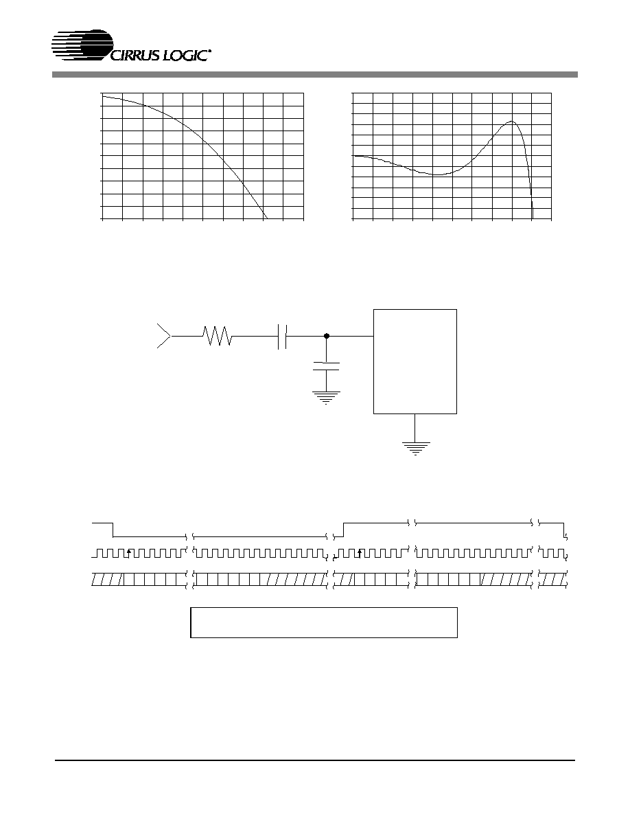
Figure 15. High-Rate Transition Band (Detail)
Figure 16. High-Rate Passband Ripple
GND
AIN_xx
150
0.47 �F
0.01 �F
Figure 17. Line Input Test Circuit
LRCK
SCLK
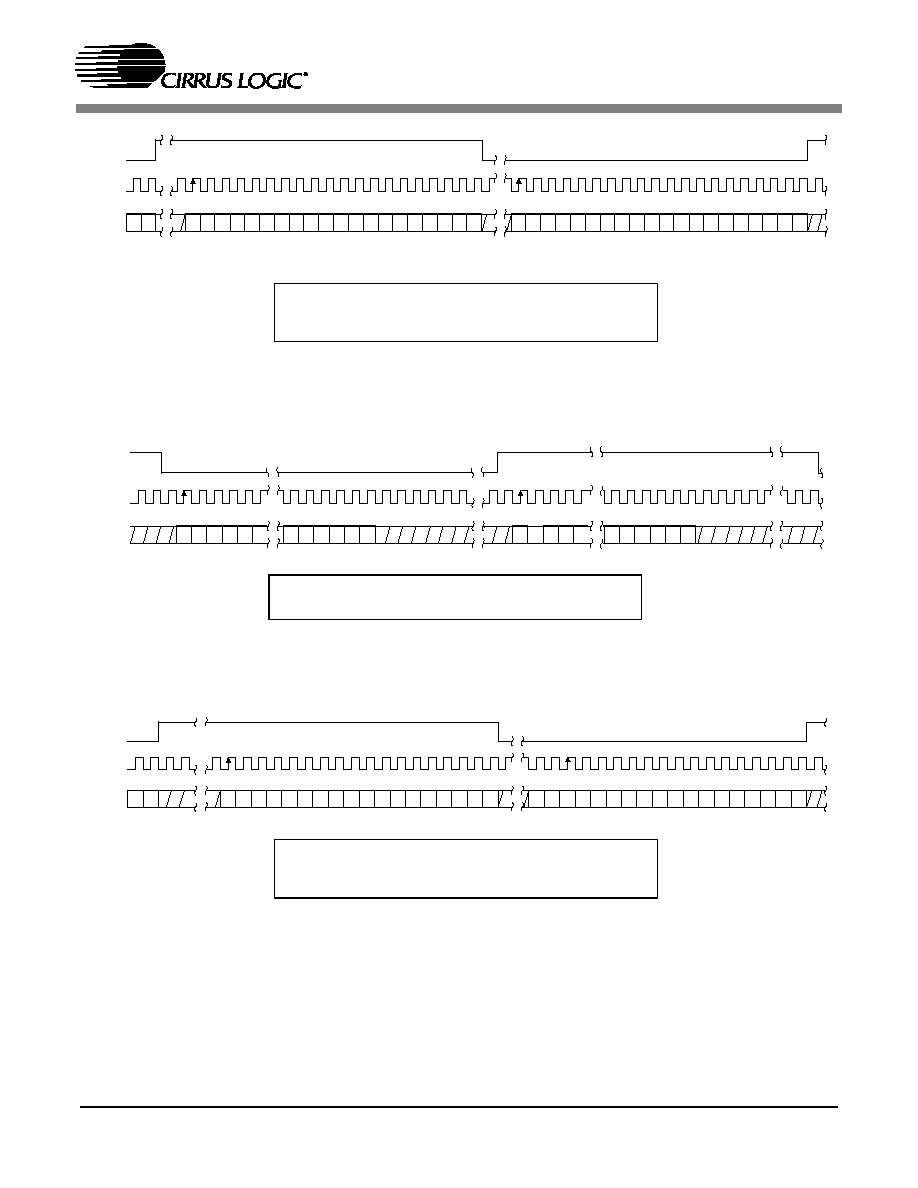
Left Channel
Right Channel
SDATA
+3 +2 +1 LSB
+5 +4
MSB -1 -2 -3 -4 -5
+3 +2 +1 LSB
+5 +4
MSB -1 -2 -3 -4
I
2
S, up to 24-Bit Data. Data Valid on Rising Edge of
SCLK.
Figure 18. CS53L32A Control Port Mode - Serial Audio Format 0 (I
2
S)

CS53L32A
DS513F1
35
LRCK
SCLK
Left Channel
Right Channel
SDATA
+3 +2 +1 LSB
+5 +4
MSB -1 -2 -3 -4 -5
+3 +2 +1 LSB
+5 +4
MSB -1 -2 -3 -4
Left Justified, up to 24-Bit Data. Data Valid on Rising
Edge of SCLK.
Figure 19. CS53L32A Control Port Mode - Serial Audio Format 1
LRCK
SCLK
Left Channel
Right Channel
SDATA
6
5
4
3
2
1
0
9
8
7
15 14 13 12 11 10
6
5
4
3
2
1
0
9
8
7
15 14 13 12 11 10
32 clocks
Right Justified, 16-Bit Data. Data Valid on Rising Edge of
SCLK. SCLK Must Have at Least 32 Cycles per LRCK
Period.
Figure 20. CS53L32A Control Port Mode - Serial Audio Format 3
Figure 21. CS53L32A Control Port Mode - Serial Audio Format 4
LRCK
SCLK
Left Channel
SDATA
6
5
4
3
2
1
0
7
23 22 21 20 19 18
6
5
4
3
2
1
0
7
23 22 21 20 19 18
32 clocks
0
Right Channel
Right Justified, 24-Bit Data. Data Valid on Rising Edge of
SCLK. SCLK Must Have at Least 48 Cycles per LRCK
Period.
CS53L32A
36
DS513F1
LRCK
SCLK
Left Channel
Right Channel
SDATA
6
5
4
3
2
1
0
9
8
7
15 14 13 12 11 10
1
0
6
5
4
3
2
1
0
9
8
7
15 14 13 12 11 10
17 16
17 16
32 clocks
Figure 22. CS53L32A Control Port Mode - Serial Audio Format 5
Right Justified, 18-Bit Data.
Data Valid on Rising Edge of SCLK.
SCLK Must Have at Least 36 Cycles per LRCK Period.
LRCK
SCLK
Left Channel
Right Channel
SDATA
6
5
4 3
2
1
0
9
8
7
15 14 13 12 11 10
1
0
6
5
4
3
2
1
0
9
8
7
15 14 13 12 11 10
17 16
17 16
32 clocks
19 18
19 18
Right Justified, 20-Bit Data. Data Valid on Rising Edge of
SCLK. SCLK Must Have at Least 40 Cycles per LRCK
Period.
Figure 23. CS53L32A Control Port Mode - Serial Audio Format 6
LRCK
SCLK
Left Channel
Right Channel
SDATA
+3 +2 +1 LSB
+5 +4
MSB
-1 -2 -3 -4 -5
+3 +2 +1 LSB
+5 +4
MSB
-1 -2 -3 -4
I
2
S, up to 24-Bit Data. Data Valid on Rising Edge of
SCLK
Figure 24. CS53L32A Stand-Alone Mode - Serial Audio Format 0 (I
2
S)

CS53L32A
DS513F1
37
LRCK
SCLK
Left Channel
Right Channel
SDATA
+3 +2 +1 LSB
+5 +4
MSB
-1 -2 -3 -4 -5
+3 +2 +1 LSB
+5 +4
MSB
-1 -2 -3 -4
Left Justified, up to 24-Bit Data. Data Valid on Rising
Edge of SCLK.
Figure 25. CS53L32A Stand-Alone Mode - Serial Audio Format 1

CS53L32A
38
DS513F1
8. PARAMETER DEFINITIONS
Total Harmonic Distortion + Noise (THD+N)
The ratio of the rms value of the signal to the rms sum of all other spectral components over the specified
bandwidth (typically 10 Hz to 20 kHz), including distortion components. Expressed in decibels.
Dynamic Range
The ratio of the full scale rms value of the signal to the rms sum of all other spectral components over the
specified bandwidth. Dynamic range is a signal-to-noise measurement over the specified bandwidth
made with a -60 dBFS signal. 60 dB is then added to the resulting measurement to refer the measurement
to full scale. This technique ensures that the distortion components are below the noise level and do not
effect the measurement. This measurement technique has been accepted by the Audio Engineering So-
ciety, AES17-1991, and the Electronic Industries Association of Japan, EIAJ CP-307.
Interchannel Isolation
A measure of crosstalk between the left and right channels. Measured for each channel at the converter's
output with all zeros to the input under test and a full-scale signal applied to the other channel. Units in
decibels.
Interchannel Gain Mismatch
The gain difference between left and right channels. Units in decibels.
Gain Error
The deviation from the nominal full scale analog output for a full scale digital input.
Gain Drift
The change in gain value with temperature. Units in ppm/�C.
9. REFERENCES
1. "How to Achieve Optimum Performance from Delta-Sigma A/D & D/A Converters" by Steven Harris.
Paper presented at the 93rd Convention of the Audio Engineering Society, October 1992.
2. CDB53L32 Evaluation Board Datasheet.
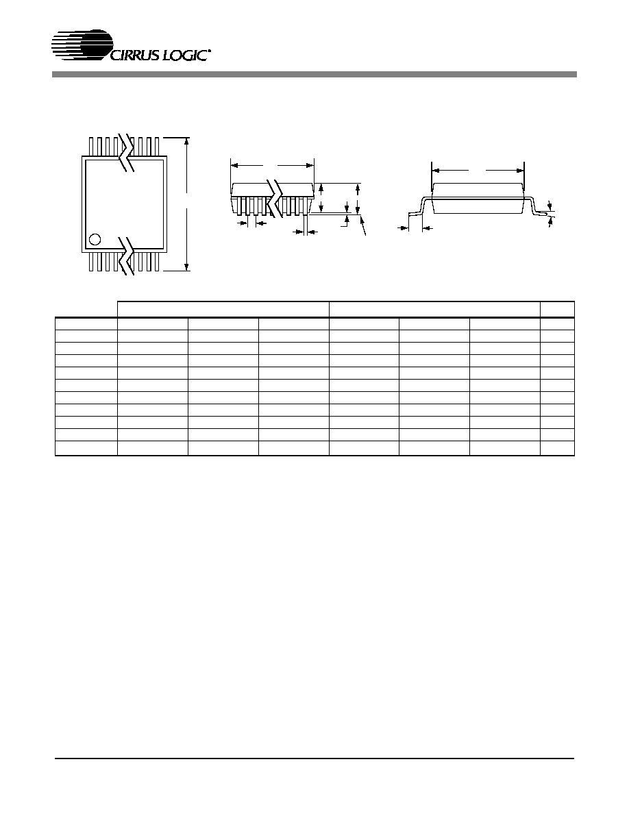
CS53L32A
DS513F1
39
10.PACKAGE DIMENSIONS
Notes: 1. "D" and "E1" are reference datums and do not included mold flash or protrusions, but do include mold
mismatch and are measured at the parting line, mold flash or protrusions shall not exceed 0.20 mm per
side.
2. Dimension "b" does not include dambar protrusion/intrusion. Allowable dambar protrusion shall be
0.13 mm total in excess of "b" dimension at maximum material condition. Dambar intrusion shall not
reduce dimension "b" by more than 0.07 mm at least material condition.
3. These dimensions apply to the flat section of the lead between 0.10 and 0.25 mm from lead tips.
INCHES
MILLIMETERS
NOTE
DIM
MIN
NOM
MAX
MIN
NOM
MAX
A
--
--
0.043
--
--
1.10
A1
0.002
0.004
0.006
0.05
--
0.15
A2
0.03346
0.0354
0.037
0.85
0.90
0.95
b
0.00748
0.0096
0.012
0.19
0.245
0.30
2,3
D
0.252
0.256
0.259
6.40
6.50
6.60
1
E
0.248
0.2519
0.256
6.30
6.40
6.50
E1
0.169
0.1732
0.177
4.30
4.40
4.50
1
e
--
--
0.026
--
--
0.65
L
0.020
0.024
0.028
0.50
0.60
0.70
0�
4�
8�
0�
4�
8�
JEDEC #: MO-153
Controlling Dimension is Millimeters.
20L TSSOP (4.4 mm BODY) PACKAGE DRAWING
E
N
1 2 3
e
b
2
A1
A2
A
D
SEATING
PLANE
E1
1
L
SIDE VIEW
END VIEW
TOP VIEW
CS53L32A
40
DS513F1
11.CHANGE HISTORY
Table 19. Revision Table
Revision
Date
Change
PP1
July 2000
Initial release
PP2
September 2004
Added part number CS53L32A-KZZ, lead free package option.
F1
October 2004
Updated Min/Max Specifications
Integrated Errata ER513B1
Integrated Errata ER513B2
Integrated Errata ER513C1
Contacting Cirrus Logic Support
For a complete listing of Direct Sales, Distributor, and Sales Representative contacts, visit the Cirrus Logic web site at:
http://www.cirrus.com/
Cirrus Logic, Inc. and its subsidiaries ("Cirrus") believe that the information contained in this document is accurate and reliable. However, the information is subject
to change without notice and is provided "AS IS" without warranty of any kind (express or implied). Customers are advised to obtain the latest version of relevant
information to verify, before placing orders, that information being relied on is current and complete. All products are sold subject to the terms and conditions of sale
supplied at the time of order acknowledgment, including those pertaining to warranty, patent infringement, and limitation of liability. No responsibility is assumed by
Cirrus for the use of this information, including use of this information as the basis for manufacture or sale of any items, or for infringement of patents or other rights
of third parties. This document is the property of Cirrus and by furnishing this information, Cirrus grants no license, express or implied under any patents, mask work
rights, copyrights, trademarks, trade secrets or other intellectual property rights. Cirrus owns the copyrights associated with the information contained herein and
gives consent for copies to be made of the information only for use within your organization with respect to Cirrus integrated circuits or other products of Cirrus. This
consent does not extend to other copying such as copying for general distribution, advertising or promotional purposes, or for creating any work for resale.
CERTAIN APPLICATIONS USING SEMICONDUCTOR PRODUCTS MAY INVOLVE POTENTIAL RISKS OF DEATH, PERSONAL INJURY, OR SEVERE PROP-
ERTY OR ENVIRONMENTAL DAMAGE ("CRITICAL APPLICATIONS"). CIRRUS PRODUCTS ARE NOT DESIGNED, AUTHORIZED OR WARRANTED FOR USE
IN AIRCRAFT SYSTEMS, MILITARY APPLICATIONS, PRODUCTS SURGICALLY IMPLANTED INTO THE BODY, LIFE SUPPORT PRODUCTS OR OTHER
CRITICAL APPLICATIONS (INCLUDING MEDICAL DEVICES, AIRCRAFT SYSTEMS OR COMPONENTS AND PERSONAL OR AUTOMOTIVE SAFETY OR SE-
CURITY DEVICES). INCLUSION OF CIRRUS PRODUCTS IN SUCH APPLICATIONS IS UNDERSTOOD TO BE FULLY AT THE CUSTOMER'S RISK AND CIR-
RUS DISCLAIMS AND MAKES NO WARRANTY, EXPRESS, STATUTORY OR IMPLIED, INCLUDING THE IMPLIED WARRANTIES OF MERCHANTABILITY
AND FITNESS FOR PARTICULAR PURPOSE, WITH REGARD TO ANY CIRRUS PRODUCT THAT IS USED IN SUCH A MANNER. IF THE CUSTOMER OR
CUSTOMER'S CUSTOMER USES OR PERMITS THE USE OF CIRRUS PRODUCTS IN CRITICAL APPLICATIONS, CUSTOMER AGREES, BY SUCH USE, TO
FULLY INDEMNIFY CIRRUS, ITS OFFICERS, DIRECTORS, EMPLOYEES, DISTRIBUTORS AND OTHER AGENTS FROM ANY AND ALL LIABILITY, INCLUD-
ING ATTORNEYS' FEES AND COSTS, THAT MAY RESULT FROM OR ARISE IN CONNECTION WITH THESE USES.
Cirrus Logic, Cirrus, and the Cirrus Logic logo designs are trademarks of Cirrus Logic, Inc. All other brand and product names in this document may be trademarks
or service marks of their respective owners.