| –≠–ª–µ–∫—Ç—Ä–æ–Ω–Ω—ã–π –∫–æ–º–ø–æ–Ω–µ–Ω—Ç: CDB61581 | –°–∫–∞—á–∞—Ç—å:  PDF PDF  ZIP ZIP |
Document Outline
- CDB61581: Universal Line Interface Unit
- Features
- Description
- TABLE OF CONTENTS
- LIST OF FIGURES
- LIST OF TABLES
- Contacting Cirrus Logic Support
- 1. POWER SUPPLY
- 2. BOARD CONFIGURATION
- 2.1. Hardware Mode
- 2.2. Hardware-Coder Mode
- 2.3. Host Mode
- 3. TRANSMIT CIRCUIT
- 4. RECEIVE CIRCUIT
- 5. REFERENCE CLOCK
- 5.1. Quartz Crystal
- 5.2. External Reference
- 6. LED INDICATORS
- 7. BUFFERING
- 8. TRANSFORMER SELECTION
- Table 2. Transformer and Resistor Options
- 9. PROTOTYPING AREA
- 10. EVALUATION HINTS
- Table 3. Jumper Selections
- 11. CDB61581 SOFTWARE
- 11.1. Configure PC
- 11.2. Configure Part
- 11.3. Control Register Configuration
- Figure 1. Register Configuration Window
- 11.4. Transmitter Ram Configuration
- Figure 2. Transmitter RAM Configuration Window
- Modify Unit Interval
- Read from File
- Load to File
- Read from RAM
- Write to RAM
- Exit
- 11.5. Modify Unit Interval
- Figure 3. Modify Unit Interval Window
- Figure 4. CDB61581 Evaluation Board Schematic
- Figure 5. Board Layout - Top Layer
- Figure 6. Board Layout - Bottom Laver
- Figure 7. Evaluation Board Silkscreen
Preliminary Product Information
This document contains information for a new product.
Cirrus Logic reserves the right to modify this product without notice.
1
Copyright
©
Cirrus Logic, Inc. 1999
(All Rights Reserved)
P.O. Box 17847, Austin, Texas 78760
(512) 445 7222 FAX: (512) 445 7581
http://www.cirrus.com
Features
s
Socketed CS61581 Universal Line Interface
s
All Required Components for CS61581 Evaluation
s
LED Status Indications for Alarm Conditions and
Operating Status
s
Support for Hardware and Host Modes
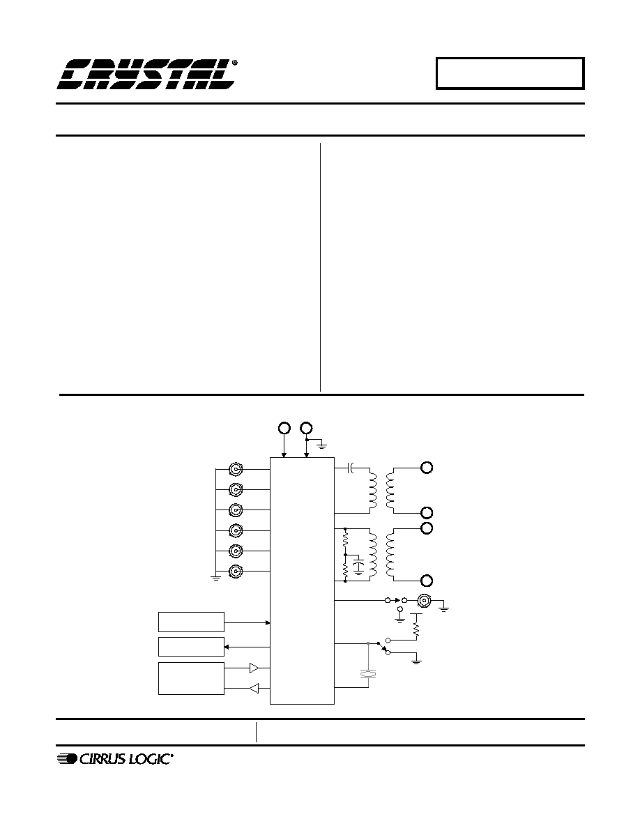
Description
The evaluation board includes a socketed CS61581 line
interface device and all support components necessary
for evaluation. The board is powered by an external
+5 Volt supply.
The board may be configured for 100
twisted-pair T1,
75
coax E1, or 120
twisted-pair E1 short and long
haul operations. Binding posts and bantam jacks are
provided for the line interface connections. Several
BNC connectors provide clock and data I/O at the sys-
tem interface. Reference timing may be derived from a
quartz crystal or an external reference clock. Four LED
indicators monitor device alarm conditions and operat-
ing status.
ORDERING INFO:
CDB61581
TTIP
RTIP
5V+
0V
TCLK
TPOS
TNEG
RCLK
RPOS
RNEG
Hardware Control
and Mode Circuit
LED Status
Indicators
Serial Interface
Control Circuit
CS61581
XTL
MCLK
XTALOUT
XTALIN
+5V
4.7 k
TRING
RRING
(optional)
OCT `99
DS211DB2
Universal Line Interface Unit
CDB61581

CDB61581
2
DS211DB2
TABLE OF CONTENTS
1.
POWER SUPPLY ................................................................................................ 3
2.
BOARD CONFIGURATION ................................................................................. 3
2.1.
Hardware Mode .......................................................................................... 3
2.1.1.
Network Loopback ......................................................................... 3
2.2.
Hardware-Coder Mode ............................................................................... 3
2.3.
Host Mode .................................................................................................. 3
3.
TRANSMIT CIRCUIT ........................................................................................... 4
4.
RECEIVE CIRCUIT .............................................................................................. 4
5.
REFERENCE CLOCK ......................................................................................... 4
5.1.
Quartz Crystal ............................................................................................. 4
5.2.
External Reference ..................................................................................... 4
6.
LED INDICATORS ............................................................................................... 5
7.
BUFFERING ........................................................................................................ 5
8.
TRANSFORMER SELECTION ............................................................................ 5
9.
PROTOTYPING AREA ........................................................................................ 5
10. EVALUATION HINTS .......................................................................................... 6
11. CDB61581 SOFTWARE ...................................................................................... 7
11.1. Configure PC .............................................................................................. 7
11.2. Configure Part ............................................................................................. 7
11.3. Control Register Configuration ................................................................... 7
11.4. Transmitter Ram Configuration ................................................................... 9
11.5. Modify Unit Interval ................................................................................... 10
LIST OF FIGURES
Figure 1. Register Configuration Window ......................................................................... 8
Figure 2. Transmitter RAM Configuration Window ........................................................... 9
Figure 3. Modify Unit Interval Window ............................................................................ 10
Figure 4. CDB61581 Evaluation Board Schematic ........................................................ 11
Figure 5. Board Layout - Top Layer ............................................................................... 12
Figure 6. Board Layout - Bottom Laver .......................................................................... 13
Figure 7. Evaluation Board Silkscreen ........................................................................... 14
LIST OF TABLES
Table 1. LATN Settings ...................................................................................................... 5
Table 2. Transformer and Resistor Options ....................................................................... 5
Table 3. Jumper Selections................................................................................................ 6
Contacting Cirrus Logic Support
For a complete listing of Direct Sales, Distributor, and Sales Representative contacts, visit the Cirrus Logic web site at:
http://www.cirrus.com/corporate/contacts/
Preliminary product information describes products which are in production, but for which full characterization data is not yet available. Advance product infor-
mation describes products which are in development and subject to development changes. Cirrus Logic, Inc. has made best efforts to ensure that the information
contained in this document is accurate and reliable. However, the information is subject to change without notice and is provided "AS IS" without warranty of
any kind (express or implied). No responsibility is assumed by Cirrus Logic, Inc. for the use of this information, nor for infringements of patents or other rights
of third parties. This document is the property of Cirrus Logic, Inc. and implies no license under patents, copyrights, trademarks, or trade secrets. No part of
this publication may be copied, reproduced, stored in a retrieval system, or transmitted, in any form or by any means (electronic, mechanical, photographic, or
otherwise) without the prior written consent of Cirrus Logic, Inc. Items from any Cirrus Logic website or disk may be printed for use by the user. However, no
part of the printout or electronic files may be copied, reproduced, stored in a retrieval system, or transmitted, in any form or by any means (electronic, mechanical,
photographic, or otherwise) without the prior written consent of Cirrus Logic, Inc.Furthermore, no part of this publication may be used as a basis for manufacture
or sale of any items without the prior written consent of Cirrus Logic, Inc. The names of products of Cirrus Logic, Inc. or other vendors and suppliers appearing
in this document may be trademarks or service marks of their respective owners which may be registered in some jurisdictions. A list of Cirrus Logic, Inc. trade-
marks and service marks can be found at http://www.cirrus.com.

CDB61581
DS211DB2
3
1. POWER SUPPLY
As shown on the evaluation board schematic in
Figure 1, power is supplied to the board from an ex-
ternal +5 Volt supply connected to the two binding
posts labeled V+ and GND. Zener diode Z1 pro-
tects the components on the board from reversed
supply connections and over-voltage damage. Ca-
pacitor C1 provides power supply decoupling and
ferrite bead L1 helps isolate the CS61581 and buff-
er supplies. Capacitors C4, C5 and C6 provide
power supply decoupling for the CS61581. The
buffer U2 is decoupled using capacitor C15. Ferrite
bead L7 helps isolates the devices U2, U3 and U4.
2. BOARD CONFIGURATION
Slide switch S1 selects hardware, host or hardware-
coder mode operation by sliding it into HW, SW or
HWCDR positions, respectively.
2.1. Hardware Mode
In Hardware mode operation, the evaluation board
is configured using the DIP switch SW1. In this
mode, the switch establishes the digital control in-
puts for both line interface channels. Closing a DIP
switch away from the label sets the CS61581 con-
trol pin of the same name to a logic 1. The host pro-
cessor interface J1 should not be used in the
Hardware mode.
The CDB61581 switches and functions are listed
below:
-
TAOS: transmit all ones;
-
LLOOP: local loopback;
-
RLOOP: remote loopback;
-
JASEL: jitter attenuator path selection;
-
LBO1, LBO2: line build out settings.
All switch inputs are pulled-high using resistor net-
work RN1.
2.1.1. Network Loopback
NLOOP is enabled in the hardware mode by clos-
ing HDR11 (HW_NLOOP) and then pressing S2. It
can also be done by sliding the switches RLOOP,
LLOOP and TAOS on SW1 towards the labels,
pulling them high, and then pulling them back to
low by sliding RLOOP, LLOOP and TAOS to OFF
(away from the labels), in that order. NLOOP can
then be turned on by sending 1-in-5 pattern on the
RTIP and RRING pins for five seconds. The
NLOOP LED will light up at this point if HDR6 is
jumped to NLOOP_LED position. NLOOP can be
turned off by sending a 1-in-3 pattern on the pins
RTIP and RRING or five seconds.
2.2. Hardware-Coder Mode
This mode is essentially the same as the Hardware
mode with the B8ZS or HDB3 encoder/decoder en-
abled.
2.3. Host Mode
In Host mode operation, the evaluation board sup-
ports serial-port operation over interface port J1 us-
ing the printer port of a host PC running the
enclosed software. The evaluation board is con-
nected to the host PC using a DB-25 male-to-male
cable (included). Ferrite beads L2-L6 help reduce
incoming noise from the host interface. The SW1
switch must be open (all switches slid away from
the labels) to enable serial-port operation.
An external microprocessor may also interface to
the evaluation board to facilitate system software
development. The CS61581 interrupt pin, INT, is

CDB61581
4
DS211DB2
3. TRANSMIT CIRCUIT
The transmit clock and data signals are supplied on
BNC inputs labeled TCLK, TPOS, and TNEG. In
Hardware and Host mode (with coder mode dis-
abled), data is supplied on the TPOS and TNEG
BNC inputs. In Host mode with coder mode en-
abled, data is supplied on the TDATA BNC input.
The transmitter output is transformer coupled to the
line through the step-up transformer T2. The signal
is available at either the Transmit binding posts
(J11, J13) or the Transmit bantam jack. Capacitor
C12 prevents output stage imbalances from pro-
ducing a DC current that may saturate the trans-
former, thus degrading its performance.
4. RECEIVE CIRCUIT
The receive signal is input at either the Receive
binding posts (J4, J10) or the Receive bantam jack.
The receive signal is transformer coupled to the
CS61581 through 1:1 transformer T1.
The receive line is terminated by resistors R1-R2 to
provide impedance matching and receiver return
loss. They are socketed so the values may be
changed according to the application. The evalua-
tion board is supplied from the factory with 50
resistors for terminating
100
twisted-pair T1
lines, 60
resistors for terminating 120
twisted-
pair E1 lines, and 37.5
resistors
for terminating
75
coaxial E1 lines. Capacitor C3 provides an
AC ground reference for the differential input.
The recovered clock and data signals are available
on BNC outputs labeled RCLK, RPOS, and RNEG.
In Hardware and Host mode (with coder mode dis-
abled), data is available on the RPOS and RNEG
BNC. With coder mode enabled, data is available
on the RDATA BNC output in unipolar format and
bipolar violations are reported on the RNEG BNC
connector.
5. REFERENCE CLOCK
The CDB61581 requires a T1 or E1 reference clock
for operation. This clock can be supplied by either
a quartz crystal or an external reference. The eval-
uation board is supplied from the factory with two
quartz crystals for T1 and E1 operations, respec-
tively. In the case that both the external reference
and the quartz crystal are applied, the external ref-
erence takes precedence.
5.1. Quartz Crystal
A quartz crystal may be inserted at socket Y1. The
quartz crystals operate at 4X the frequency of oper-
ation i.e. the T1 quartz crystal runs at 6.176 MHz
and the E1 quartz crystal at 8.192 MHz.
5.2. External Reference
An external reference of 1.544 MHz or 2.048 MHz
may be provided at the REFCLK BNC input for T1
or E1 applications, respectively. Header HDR7
must be jumpered in the "MCLK" position to pro-
vide connectivity to the MCLK pin of the
CS61581.
CDB61581
DS211DB2
5
6. LED INDICATORS
The four-LED pack D1 indicates signal states on
LATN1, LATN2, LOS and NLOOP. The LOS
LED indicator illuminates when the line interface
receiver has detected a loss of signal. The NLOOP
LED indicates if Network Loopback is in opera-
tion. The LATN1/LATN2 LED's indicate the at-
tenuation level of the received signal; reading how
much the incoming signal is below the nominal ex-
pected signal level. See Table 1 for details.
7. BUFFERING
Buffer U2 provides additional drive capability for
the SW1 and Host mode connections. The buffer
outputs are filtered with an (optional) RC network
(not initially populated) to reduce the transients
caused by buffer switching.
8. TRANSFORMER SELECTION
The evaluation board is supplied from the factory
with PE-64936 (1:1), PE-65351 (1:2) and T-1054
(1:1.5) transformers by Pulse Engineering. The
socket T1 on the board is for receive side trans-
former and T2 is for the transmit side. In the
matched impedance mode HDR1-HDR2 should be
placed in the MATZ positions, and in the low im-
pedance mode in the LOWZ positions. Please see
Table 2 for details on transformers selection.
9. PROTOTYPING AREA
An ample prototyping area with power supply and
ground connections is provided on the evaluation
board. This area can be used to develop and test a
variety of additional circuits such as framer devic-
es, system synchronizer PLLs, or specialized inter-
face logic.
LATN1
LATN2
Attenuation Level (dB)
ON
ON
0
OFF
OFF
7.5
ON
OFF
15
OFF
ON
22.5
Table 1. LATN Settings
SH=Short Haul; LH = Long Haul; Mat Z = Matched Impedance; Low Z = Low Impedance
* Default setting from the factory; **R3-R4 are shorted by placing HDR1-HDR2 in MATZ positions.
Mode
TX Transformer
RX Transformer
R1-R2
R3-R4
T1 (100
)/LH/Low Z*
1:2
1:1
50
12.5
E1 (120
)/LH/Low Z
1:2
1:1
60
15
T1 (100
)/SH/Mat Z
1:1.5
1:1
50
0**
E1 (75
)/SH/Mat Z
1:1.5
1:1
37.5
0**
E1 (120
)/SH/Mat Z
1:1.5
1:1
60
0**
Table 2. Transformer and Resistor Options

CDB61581
6
DS211DB2
10. EVALUATION HINTS
1) The orientation of pin 1 for the CS61581 is
marked by a small circle on the top-left side of
the socket U1.
2) Component locations R1-R2, R3-R4, Y1, T1
and T2 must have the correct values installed
according to the application. All the necessary
components are included with the evaluation
board.
3) Closing a DIP switch on SW1 away from the
label sets the CS61581 control pin of the same
name to logic 1.
4) When performing a manual loopback of the re-
covered signal to the transmit signal at the BNC
connectors, the recovered data must be valid on
the falling edge of RCLK to properly latch the
data in the transmit direction.
5) Jumpers can be placed on header HDR4 to pro-
vide a ground reference on TRING for 75
coax E1 applications.
Properly terminate TTIP/TRING when evaluating
the transmit output pulse shape. For more informa-
tion concerning pulse shape evaluation, refer to the
Crystal application note entitled "Measurement and
Evaluation of Pulse Shapes in T1/E1 Transmission
Systems."
Jumper
Position
Junction Selected
HDR1-2
MATZ
Selects matched impedance, connecting TTIP/TRING directly to the transformer
LOWZ
Selects low impedance, connecting TTIP/TRING to the transformer through R4/R3
HDR3
X
Don't care (not populated)
HDR4
IN
Grounds TRING on the line side of the transmit transformer
HDR5
IN
Grounds the line side of RRING through C2
HDR6
INT
Host Mode operation, connects INT pin to the serial interface
NLOOP_LE
D
Hardware Mode operation, connects NLOOP pin to the LED
HDR7
GND
Grounds the MCLK pin
MCLK
Connects the MCLK pin to the BNC
HDR8
IN
Pulls the TNEG pin high, for selecting the coder mode (TCLK has to be present for
selecting the coder mode)
HDR9
XTAL-HI
Pulls the pin XTALIN high
XTAL-GND
Pulls the pin XTALIN to ground
HDR10
X
Don't care (shorted)
HDR11
OUT
Allows S2 to pull RLOOP and LLOOP high for RESET in hardware mode
IN
Allows S2 to pull RLOOP, LLOOP, and TAOS high for enabling NLOOP in hardware
mode
HDR12
X
Provides access to the serial port signals
Table 3. Jumper Selections

CDB61581
DS211DB2
7
11. CDB61581 SOFTWARE
The CDB61581 can be configured in the host/soft-
ware mode using the application CDB61581.EXE
supplied with the board. This application allows the
user to access all of the user programmable regis-
ters in the device. It runs under Windows 95 and
98.
11.1. Configure PC
This function allows the user to set the address of
the PC parallel port. The selection depends on the
configuration of the user's PC. The Plug and Play
(PnP) function of the operating system determines
this address every time the PC is powered up, but it
normally won't change the printer port address un-
less the configuration of the hardware has changed
since the PC was last powered up. There are two
ways to determine the address of the parallel port:
the safe method and the fast method.
The safe method is to double click on the My Com-
puter icon on the desktop, double click on Control
panel, then Double click on System. Select the De-
vice Manager tab, then with "View devices by
type" selected in the window that pops up, double
click on Ports (COM & LPT). Click on the Printer
Port icon that corresponds to the port that is con-
nected to the CDB61581 evaluation board, then se-
lect Properties. On the Properties window, select
the Resources tab, then read the I/O address in the
Input/Output Range field. This is the address range
to select for the CDB61581.
The fast method is to try the ports one by one, going
to the Configure Part window every time to see
which one allows the user to read from the device.
when the wrong address is selected, the bit fields in
this window will read either all zeroes or all ones.
Going to the Configure Part window automatically
issues a read command to the device, which will
cause unpredictable results if the selected LPT port
is connected to some device other than a
CDB61581 evaluation board. Before using this
method, the user is advised to disconnect all other
devices from the LPT ports.
11.2. Configure Part
Clicking on Configure_Part brings up two options:
the first is Control Register Configuration, which
gives access to the control and status registers, and
Transmitter RAM Configuration, which configures
the Arbitrary Waveform Generator (AWG). See
the CS61581 datasheet for information on pro-
gramming these registers.
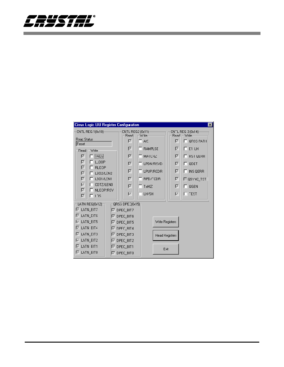
11.3. Control Register Configuration
Selecting Control Register Configuration pulls up
the register configuration window and automatical-
ly issues a read command to the CDB61581. The
user must make sure that the software is configured
to use the proper LPT port before this option is se-
lected (see Configure PC above).
The register configuration window is shown in
Figure 1. The bits in the Control Registers (CNTL
REG 1, CNTL REG 2, CNTL REG 3) are written
by checking the box opposite to the individual bits
in the "Write" columns, then clicking on the "Write
Registers" button. This writes the displayed data to
all three control registers, then automatically reads
the control and status registers and displays the re-
sults in the "Read" columns. Since Control Register
1 is effectively a control register when it is written
and a status register when it is read, the read status
is decoded and displayed in the Read Status win-
dow.
The registers can also be read by clicking on the
"Read Registers" button. All five registers are read
when this command is selected.
The LATN REG register shows the current setting
of the gain-equalizer. The QRSS DPEC register
displays the number of bit errors while receiving a
QRSS pattern.
CDB61581
8
DS211DB2
Figure 1. Register Configuration Window
CDB61581
DS211DB2
9
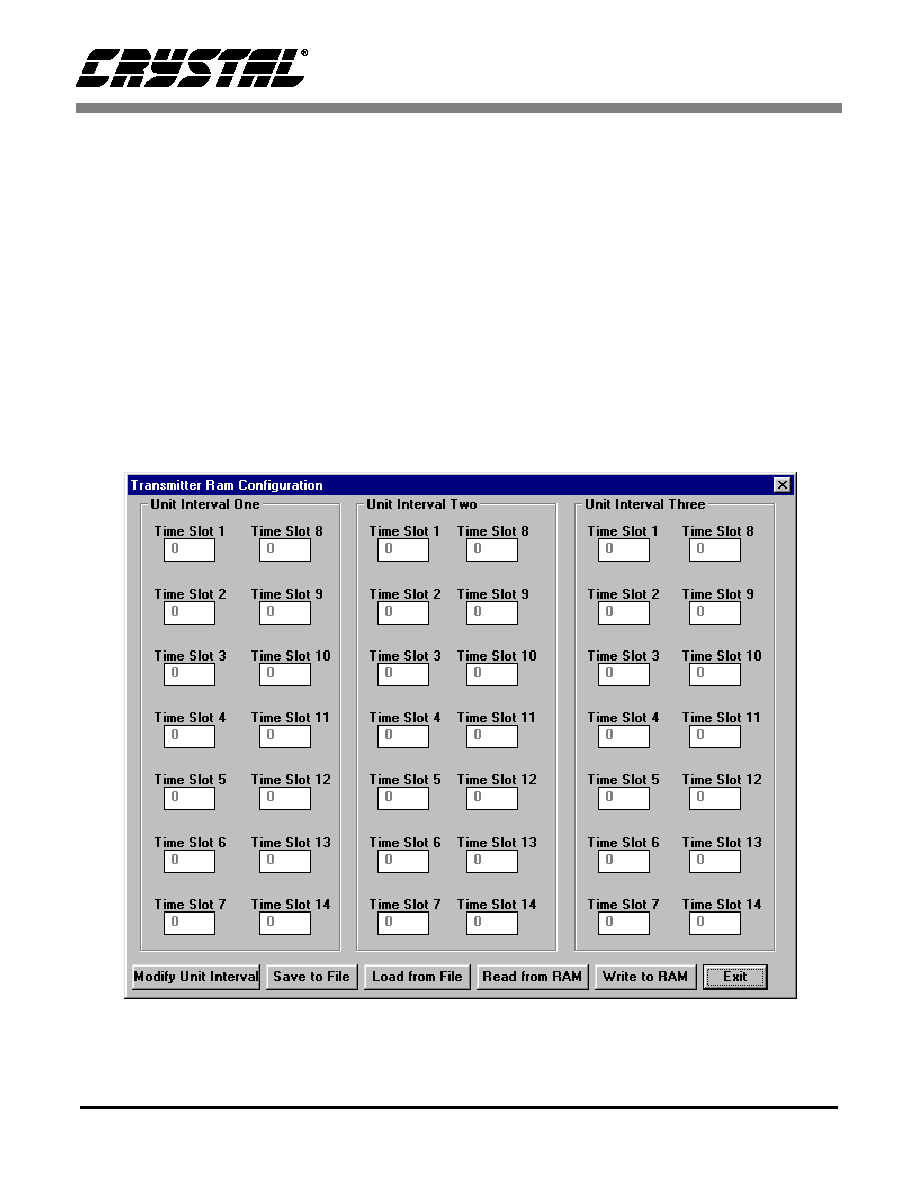
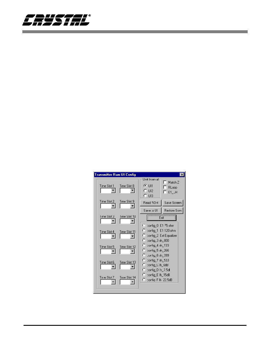
11.4. Transmitter Ram Configuration
When this command is selected, the software pops
up a window which displays the contents of the
AWG RAM (see Figure 2). Notice the six buttons
along the bottom of this window.
Modify Unit Interval brings up the Transmitter
RAM UI Config window, which allows the user to
edit the contents of the AWG registers. It is de-
scribed in the following section.
Read from File reads previously generated data
from a file.
Load to File writes the currently displayed data
into a file for later recovery using the Read from
File command.
Read from RAM reads the current data from the
AWG RAM and displays it in the current window.
Write to RAM writes the displayed data to the
AWG RAM. This must be done before exiting to
write the data to the device.
Exit returns control to the main CDB61581 menu.
It does not automatically write the data to the
CS61581.
Figure 2. Transmitter RAM Configuration Window
CDB61581
10
DS211DB2
11.5. Modify Unit Interval
The user modifies the data in the AWG RAM using
the Transmitter RAM UI Config window (see
Figure 3). At the top of this window are three radio
buttons used for selecting one of the three unit in-
tervals. At the lower right is another set of radio
buttons, one for each of the prestored waveforms in
ROM (config 0 through config f). After having se-
lected the desired UI and line configuration, click-
ing on the Read button will display the contents of
the given waveform in the Time Slot fields. These
values are displayed in hexadecimal format. The
user can modify these values by clicking on the se-
lection arrow and scrolling up and down through
the possible values. After making the necessary
modifications, the user clicks the "Save to UI" but-
ton to save the data for that UI to the PC's memory.
When all three UI's have been saved, the new val-
ues are written to the AWG RAM on the device by
going back to the Transmitter RAM Configuration
window and clicking on the Write to RAM button.
Notice that this window also has selections for the
6V pulse and Match Z buttons. These are dupli-
cates of the buttons in the LIU Configuration win-
dow. Clicking on these buttons sets or resets these
bits in the configuration registers.
These settings are reset to the initial state when the
window is closed. The Save Screen and Restore
Scrn buttons must be used if the user wishes to exit
this window and come back to the same setup.
Figure 3. Modify Unit Interval Window
CDB6
1581
DS2
11D
B2
11
FERRITE_BEAD
FERRITE_BEAD
FERRITE_BEAD
FERRITE_BEAD
FERRITE_BEAD
TAOS/CLKE
LLOOP/SCLK
RLOOP/CS
L801/SDI
NLOOP/INT
RGND
RV+
RRING
RTIP
LATN
N/C
TRING
TV+
TGND
TTIP
LOS
JASEL
XTALOUT
XTALIN
RCLK
RPOS/RDATA
RNEG/BPV
MODE
TNEG/UBS
TPOS/TDATA
NLOOP
LOS
LATN2
LATN1
RRING
J11
J13
NLOOP
J3
CON_RTT87
HW
SW
GND
.1UF
C14
GND
RNEG
TNEG
TPOS
TCLK
MCLK
GND
L1
FERRITE_BEAD
BNC
J12
BNC
J8
J9
BNC
BNC
J6
BNC
J5
P6KE6V8P
Z1
GND
1
3
5
6
2
1
3
5
6
2
J2
BNC
/G1
/G2
A1
A2
A3
A4
A5
A6
A7
A8
VCC
GND
Y1
Y2
Y3
Y4
Y5
Y6
Y7
Y8
1
2
3
4
5
6
7
8
9
10
11
12
13
14
15
16
17
18
19
20
SN74HCT541N
U2
LLOOP
RLOOP
+5V
J19
GND
GND
4
3
2
1
HDR7
1
2
3
4
HDR6
GND
GND
GND
GND
RCLK
RPOS
J7
BNC
GND
+5V
LOWZ
LOWZ
4
3
1
2
S1
SW_SP3T
25
24
23
22
21
20
19
18
17
16
15
14
13
12
11
10
9
8
7
6
5
4
3
2
1
DB25F_RA
J1
5
4
3
2
1
J3
CON_RTT87
RN1
LBO2
LBO1
6
5
4
3
2
1
OPEN
SW_DIP_6
SW1
JASEL
S2
D6
D8
+5V
HW
GND
+5V
+5V
+5V
J18
J4
J10
GND
SDO
GND
LED_555_5003
D1
CS
INT
+5V
2
1
HDR4
HDR1X2
TCLK
MCLK
L802/
CS61581
1
2
HDR8
TNEG_HI
JP8
V+
GND
LATN
LATN
RTIP
RRING
TRING
RPOS
RCLK
JP9
TAOS
TTIP
RNEG
MCLK
TCLK
TPOS
TNEG
TRING
TTIP
10
9
8
7
6
5
4
3
2
1
HDR5X2
HDR12
L2
L3
L4
L5
L6
R13
100
HDR11
2
1
HDR1X2
HDR10
COG
47
R7
47
R8
L7
FERRITE_BEAD
R9
47
COG
47
R10
COG
R11
47
COG
R5
4.7K
.1UF
C13
C1
47UF
R1
49.9
C3
C4
.1UF
C5
.1UF
C6
47UF
1
2
HDR3
4
3
2
1
RCLK
24
23
22
21
20
19
18
17
16
15
14
13
12
11
10
9
8
7
6
5
4
3
2
1
PALCE20RA10H
U3
TP1
TP2
1
2
3
4
COG
U4
4
3
U4
U4
U4
MC74F14N
11
10
MC74F14N
U4
12
13
MC74F14N
U4
SDO
28
27
26
25
24
23
22
21
20
19
18
17
16
15
14
13
12
11
10
9
8
7
6
5
4
3
2
1
SKT_PLCC28_ECM
U1
C15
.1UF
GND
GND
HWCDR
NLOOP_LED
1
2
3
4
+5V
GND
XTAL_GND
HDR9
XTAL_HI
R6
21
GND
GND
GND
GND
GND
GND
TRING
RRING
TP3
TRANSMIT
RECEIVE
47PF
C2
8
7
6
5
4
3
2
1
+5V
HWMODE
HW_RST/NLOOP
D7
1N4148
1N4148
1N4148
INT
CS
SDI
GND
COG
PE_64936
T1
HDR5
12
HDR1X2
RTIP
6
7
8
9
10
RTIP
/T-1054
PE_65351
T2
R3
12.4
R4
12.4
+5V
100PF
100PF
C8
C7
1K
GND
R12
100
SW_B3W_1100
GND
47K
100PF
100PF
100PF
C9
C10
C11
SCLK/LLOOP
SCLK
SDI
INT
SDO
6.1760MHZ
Y1
MC74F14N
+5V
49.9
R2
.47UF
V+
C12
.47UF
TTIP
TP4
MATZ
HDR1
HDR2
MATZ
5
6
8
9
MC74F14N
MC74F14N
VCC
GND
7
14
2
1
GND
GND
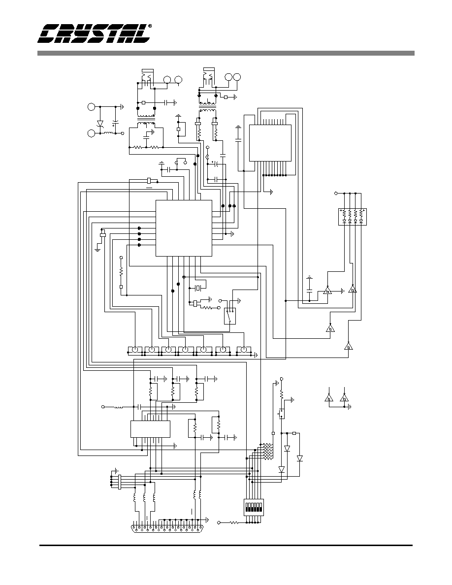
Figure 4. CDB61581 Evaluation Board Schematic
CDB6
1581
12
DS2
11DB
2
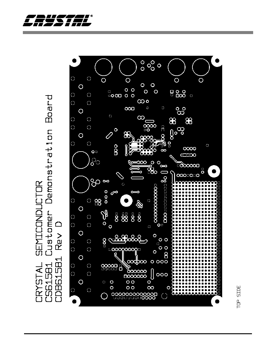
Figure 5. Board Layout - Top Layer

CDB6
1581
DS2
11D
B2
13
Figure 6. Board Layout - Bottom Laver
CDB6
1581
14
DS2
11DB
2
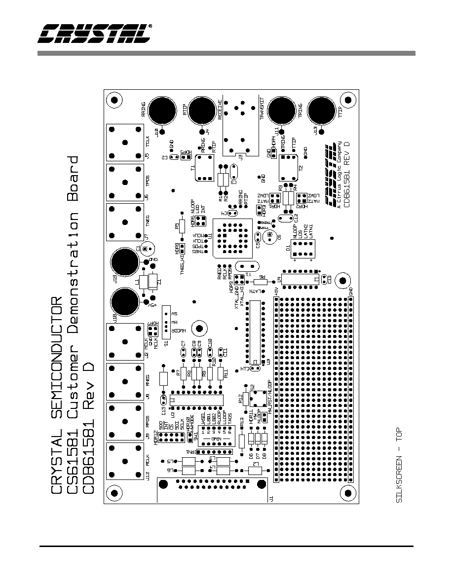
Figure 7. Evaluation Board Silkscreen

∑ Notes ∑