
Preliminary Product Information
This document contains information for a new product.
Cirrus Logic reserves the right to modify this product without notice.
1
Copyright
Cirrus Logic, Inc. 2001
(All Rights Reserved)
P.O. Box 17847, Austin, Texas 78760
(512) 445 7222 FAX: (512) 445 7581
http://www.cirrus.com
CS6422
Enhanced Full-Duplex Speakerphone IC
Features
l
Single-chip
, full-duplex, hands-free operation
l
Optional Tx Noise Guard
l
Programmable attenuation during double-talk
l
Optional 34 dB microphone preamplifier
l
Dual channel AGC'ed volume controls with
mute
l
Dual integrated 80 dB IDR codecs
l
Speech-trained Network and Acoustic Echo
Cancellers
l
Rx and Tx supplementary echo suppression
l
Configurable half-duplex training mode
l
Powerdown mode
l
Microcontroller Interface
General Description
Most modern speakerphones use half-duplex operation,
which alternates transmission between the far-end talker
and the speakerphone user. This is done to ensure sta-
bility because the acoustic coupling between the
speaker and microphone is much higher in speaker-
phones than in handsets where the coupling is
mechanically suppressed.
The CS6422 enables full-duplex conversation using
echo cancellation and suppression in a single-chip solu-
tion. The CS6422 can easily replace existing half-duplex
speakerphone ICs with a huge increase in conversation
quality.
The CS6422 consists of telephone & audio interfaces,
two codecs and an echo-cancelling DSP.
ORDERING INFORMATION
See
page 48
.
CS6422-IS
-40
o
to 85
o
C
20-pin SOIC
CDB6422
Evaluation Board
TGain
TVol
+
-
Acoustic
Echo
Canceller
ADC
Pre-emphasis
Filter
+
ASdt
DAC
+
-
Network
Echo
Canceller
Pre-emphasis
Filter
+
NSdt
DAC
ADC
Clock
Generation
Voltage
Reference
Microcontroller Interface
RGain
RVol
(0, 6, 9.5, 12 dB)
Network
Sidetone
(none, -24,
-18, -12 dB)
Acoustic
Sidetone
(none, -24,
-18, -12 dB)
1 k
Mic
34 dB
(0, 6, 9.5, 12 dB)
NI
NO
17
4
8
7
6
5
15
2
19
18
APO
API
20
CLKO
13
14
CLKI
AO
3
AVDD
DVDD
NC1
NC2
NC3
NC4
9
10
11
12
16
1
(Mute, -12 to +30 dB)
(Mute, -12 to +30 dB)
Rx
Suppression
Tx
Suppression
JUL `01
DS295PP4
Copyright
�
Cirrus Logic, Inc. 2005
(All Rights Reserved)
http://www.cirrus.com
CS6422
Enhanced Full-duplex Speakerphone IC
SEP `05
DS295F1

CS6422
2
TABLE OF CONTENTS
1. CHARACTERISTICS AND SPECIFICATIONS ........................................................................ 5
ABSOLUTE MAXIMUM RATINGS ........................................................................................... 5
RECOMMENDED OPERATING CONDITIONS ....................................................................... 5
POWER CONSUMPTION ........................................................................................................ 5
ANALOG CHARACTERISTICS ................................................................................................ 5
ANALOG TRANSMISSION CHARACTERISTICS.................................................................... 6
MICROPHONE AMPLIFIER ..................................................................................................... 6
DIGITAL CHARACTERISTICS ................................................................................................. 6
SWITCHING CHARACTERISTICS .......................................................................................... 7
2. OVERVIEW ............................................................................................................................... 9
3. FUNCTIONAL DESCRIPTION ................................................................................................. 9
3.1 Analog Interface ................................................................................................................. 9
3.1.1 Acoustic Interface ................................................................................................ 10
3.1.2 Network Interface ................................................................................................ 11
3.2 Microcontroller Interface .................................................................................................. 11
3.2.1 Description .......................................................................................................... 11
3.2.2 Register Definitions ............................................................................................. 12
3.3 Register 0 ......................................................................................................................... 13
3.3.1 Mic - Microphone Preamplifier Enable .................................................................... 14
3.3.2 HDD - Half-Duplex Disable...................................................................................... 14
3.3.3 GB - Graded Beta.................................................................................................... 14
3.3.4 RVol - Receive Volume Control............................................................................... 14
3.3.5 TSD - Transmit Suppression Disable ...................................................................... 14
3.3.6 ACC - Acoustic Coefficient Control ......................................................................... 15
3.3.7 TSMde - Transmit Suppression Mode..................................................................... 15
3.4 Register 1 ......................................................................................................................... 16
3.4.1 THDet - Transmit Half-Duplex Detection Threshold ................................................ 17
3.4.2 Taps - AEC/NEC Tap Allocation ............................................................................. 17
3.4.3 TVol - Transmit Volume Control .............................................................................. 17
3.4.4 RSD - Receive Suppression Disable....................................................................... 17
3.4.5 NCC - Network Coefficient Control.......................................................................... 17
3.4.6 AuNECD - Auto re-engage NEC Disable ................................................................ 17
3.5 Register 2 ......................................................................................................................... 18
3.5.1 RHDet - Receive Half-Duplex Detection Threshold ................................................ 19
3.5.2 RSThd - Receive Suppression Threshold ............................................................... 19
3.5.3 NseRmp - Noise estimator Ramp rate .................................................................... 19
Contacting Cirrus Logic Support
For a complete listing of Direct Sales, Distributor, and Sales Representative contacts, visit the Cirrus Logic web site at:
http://www.cirrus.com/corporate/contacts/sales.cfm
Preliminary product information describes products which are in production, but for which full characterization data is not yet available. Advance product infor-
mation describes products which are in development and subject to development changes. Cirrus Logic, Inc. has made best efforts to ensure that the information
contained in this document is accurate and reliable. However, the information is subject to change without notice and is provided "AS IS" without warranty of any
kind (express or implied). No responsibility is assumed by Cirrus Logic, Inc. for the use of this information, nor for infringements of patents or other rights of third
parties. This document is the property of Cirrus Logic, Inc. and implies no license under patents, copyrights, trademarks, or trade secrets. No part of this publi-
cation may be copied, reproduced, stored in a retrieval system, or transmitted, in any form or by any means (electronic, mechanical, photographic, or otherwise)
without the prior written consent of Cirrus Logic, Inc. Items from any Cirrus Logic website or disk may be printed for use by the user. However, no part of the
printout or electronic files may be copied, reproduced, stored in a retrieval system, or transmitted, in any form or by any means (electronic, mechanical, photo-
graphic, or otherwise) without the prior written consent of Cirrus Logic, Inc.Furthermore, no part of this publication may be used as a basis for manufacture or
sale of any items without the prior written consent of Cirrus Logic, Inc. The names of products of Cirrus Logic, Inc. or other vendors and suppliers appearing in
this document may be trademarks or service marks of their respective owners which may be registered in some jurisdictions. A list of Cirrus Logic, Inc. trade-
marks and service marks can be found at http://www.cirrus.com.
CS6422
2
DS295F1

CS6422
3
3.5.4 HDly - Half-Duplex Holdover Delay......................................................................... 19
3.5.5 HHold - Hold in Half-Duplex on Howl ...................................................................... 19
3.5.6 TDSRmp - Tx Double-talk Suppression Ramp rate ................................................ 19
3.5.7 RDSRmp - Rx Double-talk Suppression Ramp rate ............................................... 20
3.5.8 IdlTx - half-duplex Idle return-to-Transmit ............................................................... 20
3.6 Register 3 ......................................................................................................................... 21
3.6.1 TSAtt - Transmit Suppression Attenuation.............................................................. 22
3.6.2 PCSen- Path Change Sensitivity ............................................................................ 22
3.6.3 TDbtS - Tx Double-talk Suppression attenuation.................................................... 22
3.6.4 RDbtS - Rx Double-talk Suppression attenuation ................................................... 22
3.6.5 TSThd - Transmit Suppression Threshold .............................................................. 22
3.6.6 TSBias - Transmit Suppression Bias ...................................................................... 22
3.7 Register 4 ......................................................................................................................... 23
3.7.1 AErle - AEC Erle threshold...................................................................................... 24
3.7.2 AFNse - AEC Full-duplex Noise threshold .............................................................. 24
3.7.3 NErle - NEC Erle threshold ..................................................................................... 24
3.7.4 NFNse - NEC Full-duplex Noise threshold.............................................................. 24
3.7.5 RGain - Receive Analog Gain ................................................................................. 24
3.7.6 TGain - Transmit Analog Gain ................................................................................ 24
3.8 Register 5 ......................................................................................................................... 25
3.8.1 HwlD - Howl detector Disable ................................................................................. 26
3.8.2 TD - Tone detector Disable ..................................................................................... 26
3.8.3 APCD - Acoustic Path Change detector Disable .................................................... 26
3.8.4 NPCD - Network Path Change detector Disable..................................................... 26
3.8.5 APFD/NPFD - Acoustic Pre-emphasis Filter Disable/Network
Pre-emphasis Filter Disable..................................................................................... 26
3.8.6 AECD - Acoustic Echo Canceller Disable ............................................................... 27
3.8.7 NECD - Network Echo Canceller Disable ............................................................... 27
3.8.8 ASdt - Acoustic Sidetone level ................................................................................ 27
3.8.9 NSdt - Network Sidetone level ................................................................................ 27
3.9 Reset ............................................................................................................................... 28
3.9.1 Cold Reset .......................................................................................................... 28
3.9.2 Warm Reset ........................................................................................................ 28
3.9.3 Reset Timer ........................................................................................................ 28
3.10 Clocking ......................................................................................................................... 28
3.11 Power Supply ................................................................................................................ 29
3.11.1 Power Down Mode ............................................................................................ 29
3.11.2 Noise and Grounding ........................................................................................ 29
4. DESIGN CONSIDERATIONS ................................................................................................. 31
4.1 Algorithmic Considerations .............................................................................................. 31
4.1.1 Full-Duplex Mode ................................................................................................ 31
4.1.1.1 Theory of Operation ........................................................................... 31
4.1.1.2 Adaptive Filter ..................................................................................... 32
4.1.1.2.1 Pre-Emphasis ............................................................................ 32
4.1.1.2.2 Graded Beta .............................................................................. 33
4.1.1.3 Update Control .................................................................................... 33
4.1.1.4 Speech Detection ................................................................................ 33
4.1.2 Half-Duplex Mode ............................................................................................... 34
4.1.2.1 Idle Return to Transmit ....................................................................... 34
4.1.3 AGC .................................................................................................................... 34
4.1.4 Suppression ........................................................................................................ 35
4.1.4.1 Transmit Suppression ......................................................................... 36
4.1.4.2 Receive Suppression .......................................................................... 36
CS6422
DS295F1
3

CS6422
4
4.1.4.3 Double-talk Attenuation ....................................................................... 36
4.1.4.4 Noise Guard ........................................................................................ 37
4.2 Circuit Design ................................................................................................................... 37
4.2.1 Interface Considerations ..................................................................................... 37
4.2.1.1 Analog Interface .................................................................................. 37
4.2.1.2 Microcontroller Interface ...................................................................... 37
4.2.2 Grounding Considerations .................................................................................. 38
4.2.3 Layout Considerations ........................................................................................ 38
4.3 System Design ................................................................................................................. 38
4.3.1 Gain Structure ..................................................................................................... 38
4.3.2 Testing Issues ..................................................................................................... 39
4.3.2.1 ERLE ................................................................................................... 39
4.3.2.2 Convergence Time .............................................................................. 40
4.3.2.3 Half-Duplex Switching ......................................................................... 40
5. PIN DESCRIPTIONS .............................................................................................................. 41
6. GLOSSARY ............................................................................................................................ 44
7. PACKAGE DIMENSIONS ....................................................................................................... 46
LIST OF FIGURES
Figure 1. CLKI Timing ................................................................................................................... 7
Figure 2. Reset Timing .................................................................................................................. 7
Figure 3. Microcontroller Interface Timing ..................................................................................... 7
Figure 4. Typical Connection Diagram (Microphone Preamplifier Enabled) ................................. 8
Figure 5. Typical Connection Diagram (Microphone Preamplifier Disabled) ................................ 8
Figure 6. Analog Interface ........................................................................................................... 10
Figure 7. Microcontroller Interface .............................................................................................. 12
Figure 8. Suggested Layout ........................................................................................................ 29
Figure 9. Ground Planes ............................................................................................................. 30
Figure 10. Simplified Acoustic Echo Canceller Block Diagram ................................................... 31
Figure 11. How the AGC works (TVol = +30 dB) ........................................................................ 35
LIST OF TABLES
Table 1. Full scale voltages for each gain stage ........................................................................... 11
Table 2. MCR Control Register Mapping ...................................................................................... 12
Table 3. Register 0 Bit Definitions................................................................................................. 13
Table 4. Register 1 Bit Definitions................................................................................................. 16
Table 5. Register 2 Bit Definitions................................................................................................. 18
Table 6. Register 3 Bit Definitions................................................................................................. 21
Table 7. Register 4 Bit Definitions................................................................................................. 23
Table 8. Register 5 Bit Definitions................................................................................................. 25
CS6422
4
DS295F1

CS6422
5
1.
CHARACTERISTICS AND SPECIFICATIONS
ABSOLUTE MAXIMUM RATINGS
WARNING: Operation beyond these limits may result in permanent damage to the device.
Normal operation is not guaranteed at these extremes.
RECOMMENDED OPERATING CONDITIONS
POWER CONSUMPTION
(T
A
= 25�C, DVDD = AVDD = 5 V, f
XTAL
= 20.480 MHz) (Note 1)
Notes: 1. AO and NO outputs are not loaded.
ANALOG CHARACTERISTICS
(T
A
= 25�C, DVDD = AVDD = 5 V, f
XTAL
= 20.480 MHz)
Notes: 2. These parameters are guaranteed by design or by characterization.
Parameter
Symbol
Min
Max
Units
DC Supply (AVDD, DVDD)
-0.3
6.0
V
Input Current (Except supply pins)
I
in
-10
+10
mA
Input Voltage
Analog
Digital
V
ina
V
ind
-0.3
-0.3
AVDD+0.3
DVDD+0.3
V
Ambient Operating Temperature
T
A
-40
85
�C
Storage Temperature
T
stg
-65
150
�C
Parameter
Symbol
Min
Typ
Max
Units
DC Supply (AVDD, DVDD)
4.5
5.0
5.5
V
Ambient Operating Temperature
Commercial
Industrial
T
AOp
0
-40
25
25
70
85
�C
Parameter
Symbol
Min
Typ
Max
Units
Power Supply Current, Analog (RST=0)
P
DA0
1
mA
Power Supply Current, Analog (RST=1)
P
DA
10
20
mA
Power Supply Current, Digital (RST=0)
P
DD0
1
mA
Power Supply Current, Digital (RST=1)
P
DD
50
80
mA
Parameter
Symbol
Min
Typ
Max
Units
Input Offset Voltage (APO, NI)
2.12
V
Output Offset Voltage (AO, NO)
2.12
V
Transmit Group Delay
(Note 2)
6
ms
Receive Group Delay
(Note 2)
6
ms
Input Impedance (APO, NI)
Z
in
1.5
M
Load Impedance (AO, NO)
Z
load
10
k
Power Supply Rejection (1 kHz)
40
dB
CS6422
DS295F1
5

CS6422
6
ANALOG TRANSMISSION CHARACTERISTICS
(T
A
= 25�C, DVDD = AVDD = 5 V, f
XTAL
=
20.480 MHz, RVol=TVol=RGain=TGain= 0 dB, HDD=TSD=RSD=1, analog inputs and outputs loaded with
resistors and capacitors as shown in the typical connection diagram, Figure 4)
MICROPHONE AMPLIFIER
(T
A
= 25�C, DVDD = AVDD = 5 V, f
XTAL
= 20.480 MHz)
DIGITAL CHARACTERISTICS
(T
A
= 25�C, DVDD = AVDD = 5 V,f
XTAL
= 20.480 MHz)
Parameter
Symbol
Min
Typ
Max
Units
Idle Channel Noise
C-Message weighted (0-4 kHz)
(Inputs grounded
C-Message weighted (0-4 kHz)
through a capacitor)
Psophometrically weighted (0-4 kHz)
-80
11
-78
-73
dBV
dBrnC0
dBm0p
Signal-to-Noise Ratio
C-Message weighted (0-4 kHz)
(1.0 V
rms,
1 kHz sine wave input)
SNR
73
80
dB
Total Harmonic Distortion
C-Message weighted (0-4 kHz)
(1.0 V
rms,
1 kHz sine wave input)
THD
0.030
0.1
%
Programmable Analog Gain
RGain/TGain = 00
RGain/TGain = 01
RGain/TGain = 10
RGain/TGain = 11
0
6
9.5
12
dB
Volume Control Stepsize (TVol/RVol)
3
dB
ADC Full-scale Voltage Input
0.9
1.0
V
rms
DAC Full-scale Voltage Output
1.0
1.2
V
rms
ADC Noise Floor
C-Message weighted (0-4 kHz)
-83
dBV
DAC Noise Floor, DAC muted C-Message weighted (0-4 kHz)
-83
dBV
Parameter
Symbol
Min
Typ
Max
Units
Gain (Z
source
= 50
)
A
mic
34
dB
Signal-to-Noise Ratio
C-Message weighted (0-4 kHz)
SNRm
70
dB
Input Impedance
Z
inm
8
k
Input Offset Voltage
V
offm
2.12
V
Parameter
Symbol
Min
Typ
Max
Units
High-Level Input Voltage
V
IH
DVDD-1.0
V
Low-Level Input Voltage
V
IL
1.0
V
Input Leakage Current
I
leak
10
�A
Input Capacitance
C
IN
5
pF
CS6422
6
DS295F1

CS6422
7
ANALOG TRANSMISSION CHARACTERISTICS
(T
A
= -40�C to 85
o
C, DVDD = AVDD = 5 V,
f
XTAL
=20.480 MHz, RVol=TVol=RGain=TGain= 0 dB, HDD=TSD=RSD=1, analog inputs and outputs loaded with
resistors and capacitors as shown in the typical connection diagram, Figure 4)
MICROPHONE AMPLIFIER
(T
A
= 25�C, DVDD = AVDD = 5 V, f
XTAL
= 20.480 MHz)
DIGITAL CHARACTERISTICS
(T
A
= 25�C, DVDD = AVDD = 5 V,f
XTAL
= 20.480 MHz)
Parameter
Symbol
Min
Typ
Max
Units
Idle Channel Noise
C-Message weighted (0-4 kHz)
(Inputs grounded
C-Message weighted (0-4 kHz)
through a capacitor)
Psophometrically weighted (0-4 kHz)
-80
11
-78
-72
dBV
dBrnC0
dBm0p
Signal-to-Noise Ratio
C-Message weighted (0-4 kHz)
(1.0 V
rms,
1 kHz sine wave input)
SNR
72
80
dB
Total Harmonic Distortion
C-Message weighted (0-4 kHz)
(1.0 V
rms,
1 kHz sine wave input)
THD
0.030
0.1
%
Programmable Analog Gain
RGain/TGain = 00
RGain/TGain = 01
RGain/TGain = 10
RGain/TGain = 11
0
6
9.5
12
dB
Volume Control Stepsize (TVol/RVol)
3
dB
ADC Full-scale Voltage Input
0.9
1.0
V
rms
DAC Full-scale Voltage Output
1.0
1.2
V
rms
ADC Noise Floor
C-Message weighted (0-4 kHz)
-83
dBV
DAC Noise Floor, DAC muted C-Message weighted (0-4 kHz)
-83
dBV
Parameter
Symbol
Min
Typ
Max
Units
Gain (Z
source
= 50
)
A
mic
34
dB
Signal-to-Noise Ratio
C-Message weighted (0-4 kHz)
SNRm
70
dB
Input Impedance
Z
inm
8
k
Input Offset Voltage
V
offm
2.12
V
Parameter
Symbol
Min
Typ
Max
Units
High-Level Input Voltage
V
IH
DVDD-1.0
V
Low-Level Input Voltage
V
IL
1.0
V
Input Leakage Current
I
leak
10
�A
Input Capacitance
C
IN
5
pF
CS6422
DS295F1
7

CS6422
8
SWITCHING CHARACTERISTICS
Parameter
Symbol
Min
Typ
Max
Units
Digital input rise time
t
rise
1.0
�s
RST low time
t
RSTL
1.0
�s
CLKI frequency
f
CLKI
20.480
MHz
CLKI duty cycle
t
LCLKI
40
50
60
%
CLKI high or low time
t
HLCLKI
19.5
ns
Min DRDY falling to DRDY falling (CLKI = 20.480 MHz)
t
DRDY
125
�s
STROBE high or low time
t
HLSTROBE
55
ns
DRDY falling to STROBE rising setup time
t
sDRDY
30
ns
DATA valid to STROBE rising setup time
t
sDATA
30
ns
STROBE rising to DATA valid hold time
t
hDATA
30
ns
STROBE rising to DRDY rising hold time
t
hDRDY
30
ns
Min RST rising to 4th extra STROBE pulse (cold reset)
t
cRST
110
ms
Max RST rising to 4th extra STROBE pulse (warm reset)
t
wRST
100
ms
1
f
CLKI
t
HLCKI
t
HLCKI
Figure 1. CLKI Timing
Bit15 Bit14
Bit2
Bit1
Bit0
DATA
DRDY
STROBE
four extra strobe pulses
1
2
3
4
RST
t
RSTL
t
cRST
t
wRST
Figure 2. Reset Timing
Bit15
DATA
DRDY
STROBE
Bit14
Bit0
t sDRDY
t sDATA
t hDATA
t hDRDY
Bit15
Bit14
t HLSTROBE
t DRDY
Figure 3. Microcontroller Interface Timing
CS6422
8
DS295F1

CS6422
9
AVDD
AGND
API
APO
MB
AO
CLKO
CLKI
STROBE
DATA
DRDY
NI
NO
DGND
DVDD
0.1
�F
10
�F
+
0.1
�F
10
�F
+
0.47
�F
10
�F
22pF
Network
Line Out
Network
Line In
From
Microcontroller
22pF
+5V Analog
0.022
�F
0.1
�F
+
RST
NC1
NC2
NC3
NC4
1
2
20
18
19
3
3300pF
12.1 k
13
14
9
10
11
12
20.480 MHz
8
6
5
7
3300 pF
6.04 k
0.47
�F
3300 pF
12.1 k
17
4
15
16
ferrite bead
Mic Bias
Speaker
Driver
CS6422
Figure 4. Typical Connection Diagram (Microphone Preamplifier Enabled)
AVDD
AGND
API
APO
MB
AO
CLKO
CLKI
STROBE
DATA
DRDY
NI
NO
DGND
DVDD
0.1
�F
10
�F
+
0.1
�F
10
�F
+
0.47
�F
10
�F
22pF
Network
Line Out
Network
Line In
From
Microprocessor
22pF
+5V Analog
0.1
�F
+
RST
NC1
NC2
NC3
NC4
1
2
20
18
19
3
3300pF
12.1 k
13
14
9
10
11
12
20.480 MHz
8
6
5
7
3300 pF
6.04 k
0.47
�F
3300 pF
12.1 k
17
4
15
16
ferrite bead
3300 pF
0.47
�F
6.04 k
CS6422
Speaker
Driver
External Mic
Preamp
Figure 5. Typical Connection Diagram (Microphone Preamplifier Disabled)
CS6422
DS295F1
9

CS6422
10
2. OVERVIEW
The CS6422 is a full-duplex speakerphone chip for
use in hands-free communications with telephony
quality audio. Common applications include
speakerphones, inexpensive video-conferencing,
and hands-free cellular phone car kits. The CS6422
requires very few external components and allows
system control through a microcontroller interface.
Hands-free communication through a microphone
and speaker typically results in acoustic feedback
or howling because the loop gain of the system ex-
ceeds unity by the time audio amplitudes are ad-
justed to a reasonable level. The solution to the
howling problem has typically been half-duplex,
where either the transmit or the receive channel is
active, never both at the same time. This prevents
instability, but diminishes the overall communica-
tion quality by clipping words and forcing each
talker to speak in turn.
Full-duplex conversation, where both transmit and
receive channels are active simultaneously, is the
conversation quality we enjoy when using hand-
sets. Full-duplex for hands-free communications is
achieved in the CS6422 using a digital signal pro-
cessing technique called "Echo Cancellation." The
end result is a more natural conversation than half-
duplex, with no awkward breaks and pauses, allow-
ing both parties to speak simultaneously.
Echo Cancellation reduces overall loop gain and
the acoustic coupling between speaker and micro-
phone. This coupling reduction prevents the annoy-
ing effect of hearing one's own delayed speech,
which is worsened when there is delay in the sys-
tem, such as vocoder delay in digital cellular
phones.
The CS6422 is a complete system implementation
of a Digital Signal Processor with RAM and pro-
gram ROM, running Echo Cancellation algorithms
developed at Crystal Semiconductor using custom-
er input, integrated with two delta-sigma codecs.
The CS6422 is intended to provide a full-duplex
speakerphone solution with a minimum of design
effort while displacing existing half-duplex speak-
erphone chips.
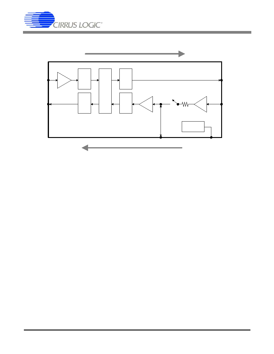
3. FUNCTIONAL DESCRIPTION
The CS6422 is divided into four external interface
blocks. The analog interfaces connect the device to
the transmit and receive paths. Control functions
are accessible through the microcontroller inter-
face. Two pins accommodate either a crystal or an
externally applied digital clock signal. Analog and
digital power and ground are provided through four
pins.
3.1
Analog Interface
In a speakerphone application, one input of the
CS6422 connects to the signal from the micro-
phone, called the near-end or transmit input, and
one output connects to the speaker. The output that
leads to the speaker is called the near-end or re-
ceive output. Together, the input and output that
connect to the microphone and speaker form the
Acoustic Interface.
The signal received at the near-end input is passed
to the far-end or transmit output after acoustic echo
cancellation. This signal is sent to the telephone
line. The signal from the telephone line is received
at the far-end input, also called the receive input,
and this signal is passed to the receive output after
network echo cancellation. The far-end input and
output form the Network Interface.
The analog interfaces are physically implemented
using delta sigma converters running at an output
word rate of 8 kHz, resulting in a passband from
DC to 4 kHz. Because the inputs are analog to dig-
ital converters (ADCs), anti-aliasing and full-scale
input voltage must be kept in mind. The ADCs ex-
pect a single-pole RC filter with a corner at 8 kHz,
and they are post-compensated internally to pre-
vent any resulting passband droop. The ADCs also
expect a maximum of 0.9 V
rms
(2.5 V
pp
) at their in-
puts (which are biased around 2.12 VDC). A signal
CS6422
10
DS295F1
CS6422
11
of higher amplitude will clip the ADC input and
will result in poor echo canceller performance. See
Section 4., "Design Considerations" for more de-
tails.
The outputs are delta-sigma digital to analog con-
verters (DACs) and have similar requirements to
the ADCs. The DACs are pre-compensated to ex-
pect a single-pole RC filter with a corner frequency
at 4 kHz. The full scale voltage output from a DAC
is 1.1 V
rms
(3.1 V
pp
) maximum, 1 V
rms
typical, bi-
ased around 2.12 VDC.
3.1.1
Acoustic Interface
The pins API (pin 20), APO (pin 18), AO (pin 3),
and MB (pin 19) form the Acoustic Interface. A
block diagram of the Acoustic Interface is shown in
Figure 6.
API and APO are, respectively, the input and out-
put of the built-in microphone pre-amplifier. The
pre-amplifier is an inverting amplifier with a fixed
gain of 34 dB biased around an input offset voltage
of 2.12 V. APO is the output of the pre-amplifier
after a 1 k
(typical) resistor. The circuitry con-
nected to the amplifier input must present low
source impedance (<100
) to the API pin or the
gain will be reduced. When using the internal mic
preamp, a 0.022
�F capacitor should be placed be-
tween APO and ground to provide the anti-aliasing
filter required by the ADC, as shown in Figure 4.
The pre-amplifier may be bypassed by clearing the
`Mic' bit (Register 0, bit 15) using the Microcontrol-
ler Interface (see Section 3.2, "Microcontroller Inter-
face"). If the internal mic preamp is not used, a
0.022
�F capacitor should be tied between API and
ground, and APO should be driven directly. In this
case, the signal into APO must be low-pass filtered
by a single-pole RC filter with a corner frequency at
8 kHz (see Figure 5).
Following the pre-amplifier is a programmable an-
alog gain stage, called TGain, which is controlled
MB
APO
20
AO
(0,6,9.5,12 dB)
ADC
DAC
DAC
ADC
D
S
P
NI
17
NO
4
FAR-END
Transmit Path
Receive Path
API
1k
Voltage
Reference
34 dB
(0,6,9.5,12 dB)
NEAR-END
3
TGain
RGain
CS6422
Mic
19
18
Figure 6. Analog Interface
CS6422
DS295F1
11

CS6422
12
through the Microcontroller Interface. This gain
stage allows gains of 0 dB, 6 dB, 9.5 dB, and 12 dB
to be added prior to the ADC input. The default
gain stage setting is 0 dB.
The signal at APO should not exceed 2.5 V
pp
at the
0 dB gain stage setting. If a different gain setting is
used, then the full-scale signal at APO must also
change. Table 1 shows full-scale voltages as mea-
sured at APO for the given programmable gain:
MB serves to provide decoupling for the internal
voltage reference, and must have a 0.1
�F and a
10
�F capacitor to ground for bypass. Noise on MB
will strongly influence the overall analog perfor-
mance of the CS6422.
The acoustic output, AO, should connect to a sin-
gle-pole low-pass RC network with a corner fre-
quency of 4 kHz, which will filter out-of-band
components. The full-scale voltage swing at AO is
3.1 V
pp
maximum, 1 V
rms
typical. AO is capable of
driving a load of 10 k
or more.
3.1.2
Network Interface
The pins NI (pin 17) and NO (pin 4) form the Net-
work Interface. The details of the Network Inter-
face are shown in Figure 6.
NI is the input from the telephone network into the
CS6422. The signal into NI must be low pass fil-
tered by a single-pole RC filter with a corner fre-
quency of 8 kHz.
RGain, a programmable analog gain stage accessi-
ble through the Microcontroller Interface, ampli-
fies signals received at NI. This gain stage allows a
gain of 0 dB, 6 dB, 9.5 dB, or 12 dB to be added
prior to the ADC input. The default gain stage set-
ting for the network side is 0 dB.
The signal at NI should not exceed 2.5 V
pp
at the
0 dB gain stage setting. If another gain setting is se-
lected, then the full-scale signal at NI will change.
Table 1 shows full-scale voltages as measured at NI
for the given programmable gain.
The output to the telephone network side, NO,
should connect to a single pole RC network with a
corner frequency at 4 kHz, which will filter out-of-
band components. The maximum swing NO is ca-
pable of producing is 3.1 V
pp
maximum, 1 V
rms
typical. NO is capable of driving a load of 10 k
or
more.
3.2
Microcontroller Interface
The registers and control functions of the CS6422
are accessible through the Microcontroller Inter-
face, which consists of three pins: DATA (pin 8),
STROBE (pin 7), and DRDY (pin 6). These inputs
can connect to the outputs of a microcontroller to
allow write-only access to the 16-bit Microcontrol-
ler Control Register (MCR).
3.2.1
Description
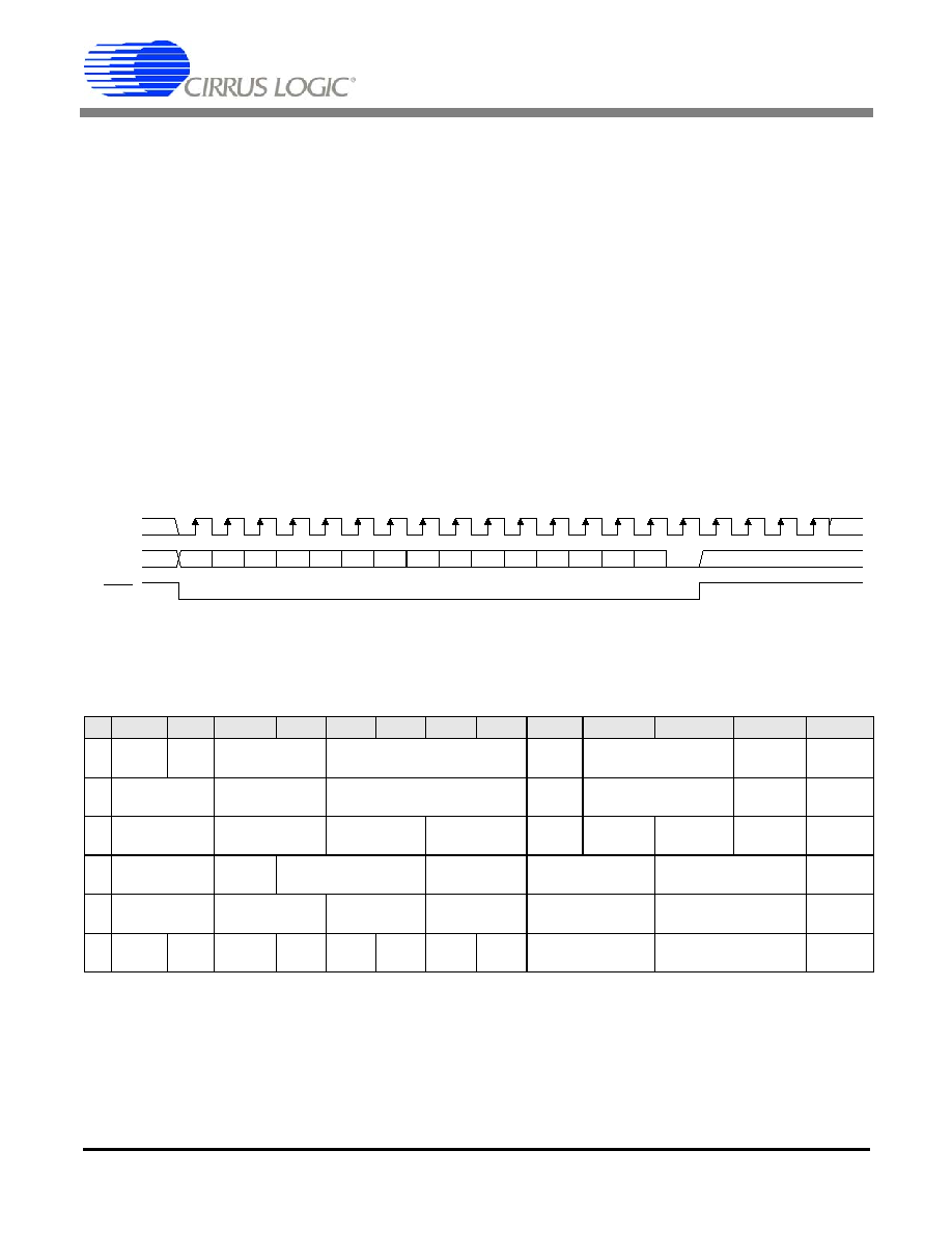
The Microcontroller Interface is implemented by a
serial shift register that is clocked by STROBE and
gated by DRDY. The microcontroller begins the
transaction by setting DRDY low while STROBE
is low. The most significant bit (MSB), Bit 15, of
the 16-bit data word should be presented to the
DATA pin and then STROBE should be brought
high to shift the data bit into the CS6422. STROBE
should be brought low again so it is ready to shift
the next bit into the shift register. The next data bit
should then be presented to the DATA pin ready to
be latched by the rising edge of STROBE. This pro-
cedure repeats for all sixteen bits as shown in Fig-
ure 7. After the last bit (Bit 0) has been shifted in,
DRDY should be brought high to indicate the con-
clusion of the transfer, and four or more extra
Gain Setting
Full-scale Voltage
0 dB
2.5 V
pp
6 dB
1.25 V
pp
9.5 dB
0.84 V
pp
12 dB
0.63 V
pp
Table 1. Full scale voltages for each gain stage
CS6422
12
DS295F1
CS6422
13
STROBE pulses must be applied to latch the data
into the CS6422.
Since the MCR is a shift register, the STROBE can
be run arbitrarily slowly with a duty cycle limited
only by the minimum high and low time specified
in "Switching Characteristics". The Microcontrol-
ler Interface is polled at 125
�s intervals, so regis-
ter writes must be spaced at least 125
�s apart or
the register contents may be overwritten.
3.2.2
Register Definitions
The six control registers accessible through the
MCR are described in detail in the following tables.
These registers are addressed by bits b3-0 of the
MCR. Bit `b0' must always be `0'. Table 2 shows
the register map with the default settings. Tables 3
through 8 show the control registers in more detail.
The Register Map at the top of each register de-
scription shows the names of all the bits, with their
reset values below the bitfield name. The reset val-
ue can also be found in the Word column of the bit-
field summary as indicated by an `*'.
#
b15
b14
b13
b12
b11
b10
b9
b8
b7
b6
b5
b4
b3-0
0
Mic
1
HDD
0
GB
10
RVol
0100
TSD
0
ACC
00
TSMde
0
0000
1
THDet
00
Taps
10
TVol
1010
RSD
0
NCC
00
AuNECD
0
0010
2
RHDet
00
RSThd
00
NseRmp
00
HDly
00
HHold
0
TDSRmp
0
RDSRmp
0
IdlTx
0
0100
3
TSAtt
00
PCSen
0
TDbtS
000
RDbtS
00
TSThd
00
TSBias
00
0110
4
AErle
00
AFNse
00
NErle
00
NFNse
00
RGain
00
TGain
00
1000
5
HwlD
0
TD
0
APCD
0
NPCD
0
APFD
0
NPFD
0
AECD
0
NECD
0
ASdt
00
NSdt
00
1010
Table 2. MCR Control Register Mapping
Bit15 Bit14 Bit13 Bit12 Bit11 Bit10
Bit9
Bit8
Bit7
Bit6
Bit5
Bit4
Bit3
Bit2
Bit1
Bit0
DATA
DRDY
STROBE
four extra strobe pulses
1
2
3
4
Figure 7. Microcontroller Interface
CS6422
DS295F1
13

CS6422
14
3.3
Register 0
b15
b14
b13
b12
b11
b10
b9
b8
b7
b6
b5
b4
b3
b2
b1
b0
Mic
HDD
GB
RVol
TSD
ACC
TSMde
0
0
0
0
1
0
10
0100
0
00
0
A
4
0
0
Bits
Name
Function
Word
Operation
15
Mic
Microphone preamplifier enable
0
1*
disable mic preamp
enable mic preamp
14
HDD
Half-Duplex Disable
0*
1
enable half-duplex
disable half-duplex
13-12
GB
Graded Beta
00
01
10*
11
0.00 dB/ms
0.75 dB/ms
0.38 dB/ms
0.19 dB/ms
11-8
RVol
Rx Volume control
0000
0001
---
0100*
---
1010
1011
---
1101
1110
1111
+30 dB
+27 dB
---
+18 dB
---
+0 dB
-3 dB
---
-9 dB
-12 dB
mute
7
TSD
Tx Suppression Disable
0*
1
enable Tx suppression
disable Tx suppression
6-5
ACC
AEC Coefficient Control
00*
01
10
11
Normal
Clear
Freeze
reserved
4
TSMde
Tx Suppression Mode
0*
1
enable noise guard
disable noise guard
* Denotes reset value
Table 3. Register 0 Bit Definitions
CS6422
14
DS295F1

CS6422
15
3.3.1
MIC - MICROPHONE PREAMPLIFIER ENABLE
The microphone preamplifier described in Section 3.1.1, "Acoustic Interface" is enabled by default,
but may be disabled by setting Mic to `0'. Refer to Section 3.1.1, "Acoustic Interface" for more details
on using the Microphone Preamplifier.
3.3.2
HDD - HALF-DUPLEX DISABLE
In normal operation, the CS6422 will be in a half-duplex mode if the echo canceller is not providing
enough loop gain reduction to prevent howling. This half-duplex mode is active at power-up while the
adaptive filter begins to train. Half-duplex mode prevents howling and also masks the convergence
process.
In some cases, such as when measuring convergence speed (see Section 4.3.2, "Testing Issues"),
the half-duplex mode is undesirable. By default, the half-duplex mode is enabled.
3.3.3
GB - GRADED BETA
The room-size adjustment scheme called "graded beta," provided for the acoustic echo canceller in
the CS6422, is controlled by GB. The network echo canceller does not support graded beta.
Graded beta is an architectural enhancement to the CS6422 which takes advantage of the fact that
acoustic echoes tend to decay exponentially with time. The CS6422 can increase the beta, or update
gain, for the coefficients of the adaptive filter which occur earlier in time and decrease it for those that
occur later in time, which increases convergence speed while maintaining stability. In order to make
this improvement, there is an implicit assumption that the decay rate of the echo is known. The graded
beta control allows the system designer to adjust this. For very acoustically live rooms, use either no
decay (00) or slight decay (11). Cars and acoustically dead rooms can benefit from the most rapid decay
(01).
3.3.4
RVOL - RECEIVE VOLUME CONTROL
Volume in the receive path is set by RVol. The volume control in the receive direction is implemented
by a peak-limiting automatic gain control (AGC) and digital attenuation at the near-end output DAC.
The AGC is discussed in detail in Section 4., "Design Considerations". See Section 4.1.3, "AGC"for a
full explanation of how it functions.
When the reference level is set to +0 dB, the AGC is disabled. Volume control is implemented by dig-
ital attenuation in 3 dB steps from this point on down. The maximum gain is +30 dB and the minimum
is -12 dB. The lowest gain setting (1111) mutes the receive path.
The default setting for RVol is +18 dB.
3.3.5
TSD - TRANSMIT SUPPRESSION DISABLE
The Transmit Supplementary Echo Suppression function is a non-linear echo control mechanism.
Transmit Suppression introduces TSAtt (see Register 3) of attenuation into the transmit path when it
is engaged. When TSMde = `1', the transmit suppressor engages when there is speech detected in
the receive path and no near-end speech is present. When TSMde = `0', the default case, the transmit
suppressor engages when there is no near-end speech present. When near-end speech is present,
the suppression attenuation is removed. By default, the transmit suppression function is enabled.
CS6422
DS295F1
15

CS6422
16
3.3.6
ACC - ACOUSTIC COEFFICIENT CONTROL
The coefficients of the AEC adaptive filters in the CS6422 are controlled by ACC. The default position
(00) yields normal operation, which means the coefficients are free to adjust themselves to the echo
path in order to cancel echo. When set to the clear position (01), the adaptive filter coefficients are all
held at zero, so the echo canceller is effectively disabled. Note that unless the half-duplex mode is
disabled, this will force the CS6422 into half-duplex mode. The freeze position (10) causes the coef-
ficients to retain their current values and not change.
3.3.7
TSMDE - TRANSMIT SUPPRESSION MODE
TSMde enables the Noise Guard feature of the CS6422. Noise Guard is a noise squelch feature that
operates in the transmit path (from the near-end microphone to the far-end speaker). In traditional
hands-free systems where the near-end talker is located in a noisy environment, the near-end system
will remain in transmit mode and send that noise to the far-end listener. This creates a real problem
if the listener is using a traditional half-duplex speakerphone because the far-end phone will stay in
receive mode, thus preventing the far-end talker from being heard. Noise Guard eliminates this prob-
lem by squelching the transmit channel at the near-end unless near-end speech is detected, permit-
ting the far-end speakerphone to switch normally during the conversation.
Noise Guard is also useful in cellular hands-free car applications because it prevents car noise from
reaching the far-end while the near-end talker is silent.
Noise Guard is usually disabled when "half-duplex Idle return-to-Transmit" is enabled. See the Reg-
ister 2 description for more information. Noise Guard is enabled by default.
CS6422
16
DS295F1

CS6422
17
3.4
Register 1
b15
b14
b13
b12
b11
b10
b9
b8
b7
b6
b5
b4
b3
b2
b1
b0
THDet
Taps
TVol
RSD
NCC
AuNECD
0
0
1
0
00
10
1010
0
00
0
2
A
0
2
Bits
Name
Function
Word
Operation
15-14
THDet
Tx Half-duplex Detection
threshold
00*
01
10
11
6 dB
9 dB
12 dB
reserved
13-12
Taps
AEC/NEC Tap allocation
00
01
10*
11
444/64 (55.5 ms/8 ms)
380/128 (47.5 ms/16 ms)
316/192 (39.5 ms/24 ms)
252/256 (31.5 ms/32 ms)
11-8
TVol
Tx Volume control
0000
0001
---
0100
---
1010*
1011
---
1101
1110
1111
+30 dB
+27 dB
---
+18 dB
---
+0 dB
-3 dB
---
-9 dB
-12 dB
mute
7
RSD
Rx Suppression Disable
0*
1
enable Rx suppression
disable Rx suppression
6-5
NCC
NEC Coefficient Control
00*
01
10
11
Normal
Clear
Freeze
reserved
4
AuNECD
Auto re-engage NEC Disable
0*
1
enable Auto NEC
disable Auto NEC
* Denotes reset value
Table 4. Register 1 Bit Definitions
CS6422
DS295F1
17

CS6422
18
3.4.1
THDET - TRANSMIT HALF-DUPLEX DETECTION THRESHOLD
The sensitivity of the speech detector controls channel switching and ownership in half-duplex mode.
The transmit speech detector registers speech if the transmit channel signal power is THDet above
the noise floor of the transmit channel.
3.4.2
TAPS - AEC/NEC TAP ALLOCATION
The CS6422 has a total of 63.5 ms of echo canceller taps that it can partition for use by the network
and acoustic echo cancellers. By default, the CS6422 allocates 39.5 ms for the AEC and 24 ms for
the NEC. See NErle, NFNse, AErle, and AFNse in Register 4, and AECD and NECD in Register 5 for
more options when an echo path is nonexistent.
3.4.3
TVOL - TRANSMIT VOLUME CONTROL
Volume in the transmit path is controlled by TVol. Like receive volume, the transmit volume is con-
trolled by an AGC. See RVol in Register 0 for more details. The default setting for TVol is +0 dB.
3.4.4
RSD - RECEIVE SUPPRESSION DISABLE
The Receive Supplementary Echo Suppression function is a non-linear echo control mechanism.
Supplementary Echo Suppression attenuates signals in the receive direction by 24 dB when far-end
speech is absent in the receive path. The attenuation is released only when the receive channel is
active. By default, the receive suppression function is enabled.
3.4.5
NCC - NETWORK COEFFICIENT CONTROL
The NEC adaptive filter's coefficients are controlled by NCC. See ACC in Register 0 for more details.
The default setting for NCC is Normal mode.
3.4.6
AUNECD - AUTO RE-ENGAGE NEC DISABLE
AuNECD works in conjunction with NFNse in the determination of whether the Network Echo Cancel-
ler should be enabled or disabled. If the CS6422 determines that a network coupling path does not
exist and disables the NEC (which can occur only if NFNse is set to a non-zero value), then AuNECD
allows the DSP to re-enable the NEC if at some point during the call a network path appears.
An example occurs in a digital PBX environment. Initially, a 4-wire `intercom' call is placed between
two stations. The CS6422 at the near-end determines that a network path is not present and disables
the NEC. During the call, one of the stations conferences in a call from an external analog line. A
network coupling path is introduced by the addition of the analog line due to the impedance mismatch
at the 2-to-4 wire converter. If AuNECD is enabled, the CS6422 at the near-end will detect the pres-
ence of the network coupling path and re-enable the NEC automatically, drop to half-duplex, and re-
train.
CS6422
18
DS295F1

CS6422
19
3.5
Register 2
b15
b14
b13
b12
b11
b10
b9
b8
b7
b6
b5
b4
b3
b2
b1
b0
RHDet
RSThd
NseRmp
HDly
HHold TDSRmp RDSRmp
IdlTx
0
1
0
0
00
00
00
00
0
0
0
0
0
0
0
4
Bits
Name
Function
Word
Operation
15-14
RHDet
Rx Half-duplex Detection threshold
00*
01
10
11
6 dB
9 dB
12 dB
reserved
13-12
RSThd
Rx Suppression Threshold
00*
01
10
11
6 dB
9 dB
12 dB
reserved
11-10
NseRmp
Noise estimator Ramp rate
00*
01
10
11
3 dB/s
6 dB/s
12 dB/s
reserved
9-8
HDly
half-duplex Holdover Delay
00*
01
10
11
200 ms
100 ms
150 ms
reserved
7
HHold
Hold in half-duplex on Howl
0*
1
disable HHold
enable HHold
6
TDSRmp
Tx Double-talk Suppression Ramp rate
0*
1
slow
normal
5
RDSRmp
Rx Double-talk Suppression Ramp rate
0*
1
slow
normal
4
IdlTx
half-duplex Idle return-to-Transmit
0*
1
disable IdlTx
enable IdlTx
* Denotes reset value
Table 5. Register 2 Bit Definitions
CS6422
DS295F1
19

CS6422
20
3.5.1
RHDET - RECEIVE HALF-DUPLEX DETECTION THRESHOLD
The sensitivity of the speech detector controls channel switching and ownership in half-duplex mode.
The receive speech detector registers speech if the receive channel signal power is RHDet above the
noise floor for the receive channel.
3.5.2
RSTHD - RECEIVE SUPPRESSION THRESHOLD
This parameter sets the threshold for far-end speech detection for disengaging receive suppression.
The speech detector that disengages the receive suppression has its sensitivity controlled by RSThd.
The suppression is inserted into the receive path unless signal from the far-end exceeds the receive
channel noise power by RSThd, in which case speech is assumed to be detected and the suppression
is defeated until speech is no longer detected. Decreasing RSThd to make the speech detector more
sensitive could result in false detections due to spurious noise events which may cause an unpleasant
noise modulation at the near-end. Increasing RSThd makes it robust to spurious noise, but may sup-
press weak far-end talkers. RSThd does not affect the ability of the receive suppressor to attenuate
residual network echo.
3.5.3
NSERMP - NOISE ESTIMATOR RAMP RATE
The background noise power estimators increase at a programmable rate until the background noise
power estimate equals the current input power estimate. The background noise power estimators
quickly track drops in the current input power estimate. Choose large values of NseRmp if the envi-
ronment is expected to have rapidly varying noise levels. Choose small values of NseRmp if the en-
vironment is expected to have relatively constant noise power.
3.5.4
HDLY - HALF-DUPLEX HOLDOVER DELAY
After a channel goes idle in the half-duplex mode of operation, a change of channel ownership is in-
hibited for HDly in order to prevent false switching due to echoes. The half-duplexor will be more im-
mune to false switching if this delay is longer, but it will also prevent a fast response to legitimate
channel changes. Short values of HDly mimic a more full-duplex like behavior, but may be succepti-
ble to false switching due to echo.
3.5.5
HHOLD - HOLD IN HALF-DUPLEX ON HOWL
This is a control flag which, if enabled, holds the system in half-duplex when a howl event is detected.
The system may transition to full-duplex if the flag is subsequently cleared. The default state of HHold
is `disabled', thus when a howl is detected, the CS6422 will temporarily drop into half-duplex, retrain,
and transition back into full-duplex on its own.
3.5.6
TDSRMP - TX DOUBLE-TALK SUPPRESSION RAMP RATE
When "Tx Double-talk Suppression attenuation" (TDbtS, Register 3) is set to a non-zero value, the
CS6422 will introduce a programmable amount of attenuation into the transmit path during a double-
talk event, that is, when the near-end talker and far-end talker are speaking simultaneously. TDSRmp
controls the decay rate of the transmit double-talk attenuation (the attack rate is ~40 ms).
The `slow' setting of TDSRmp results in an attenuation decay rate of about 1 second. The `normal'
setting of TDSRmp results in an attenuation decay rate of about 100 ms.
CS6422
20
DS295F1

CS6422
21
3.5.7
RDSRMP - RX DOUBLE-TALK SUPPRESSION RAMP RATE
When "Rx Double-talk Suppression attenuation" (RDbtS, Register 3) is set to a non-zero value, the
CS6422 will introduce a programmable amount of attenuation into the receive path during a double-
talk event. RDSRmp controls the decay rate of the receive double-talk attenuation (the attack rate is
~40 ms).
The `slow' setting of RDSRmp results in an attenuation decay rate of about 1 second. The `normal'
setting of RDSRmp results in an attenuation decay rate of about 100 ms.
3.5.8
IDLTX - HALF-DUPLEX IDLE RETURN-TO-TRANSMIT
When IdlTx is enabled, the CS6422's half-duplex engine will automatically switch into <Transmit>
mode from the <Idle> state. The <Idle> state is entered when the previously active channel has been
silent for the time period set by HDly (half-duplex Holdover Delay) in Register 2.
The use of IdlTx permits a full-duplex-like behavior when operating in half-duplex at the beginning of
a call. This benefit is most noticeable when the listener at the far end is using a handset.
When TSMde is set to `0' (Noise Guard enabled), IdlTx is usually disabled. IdlTx is disabled by de-
fault.
CS6422
DS295F1
21

CS6422
22
3.6
Register 3
b15
b14
b13
b12
b11
b10
b9
b8
b7
b6
b5
b4
b3
b2
b1
b0
TSAtt
PCSen
TDbtS
RDbtS
TSThd
TSBias
0
1
1
0
00
0
000
00
00
00
0
0
0
6
Bits
Name
Function
Word
Operation
15-14
TSAtt
Tx Suppression Attenuation
00*
01
10
11
18 dB
12 dB
24 dB
reserved
13
PCSen
Path Change Sensitivity
0*
1
high sensitivity
low sensitivity
12-10
TDbtS
Tx Double-talk Suppression
attenuation
000*
001
010
...
110
111
0 dB
3 dB
6 dB
...
18 dB
21 dB
9-8
RDbtS
Rx Double-talk Suppression
attenuation
00*
01
10
11
0 dB
3 dB
6 dB
9 dB
7-6
TSThd
Tx Suppression Threshold
00*
01
10
11
15 dB
12 dB
9 dB
18 dB
5-4
TSBias
Tx Suppression Bias
00*
01
10
11
18 dB
15 dB
21 dB
reserved
* Denotes reset value
Table 6. Register 3 Bit Definitions
CS6422
22
DS295F1

CS6422
23
3.6.1
TSATT - TRANSMIT SUPPRESSION ATTENUATION
This parameter sets the amount of attenuation inserted into the transmit path when transmit suppres-
sion is engaged.
3.6.2
PCSEN- PATH CHANGE SENSITIVITY
The Acoustic Interface is likely to have many path changes as people move about in the room where
the full-duplex speakerphone is being used. The sensitivity of the path change detector can be
changed with the PCSen bit. Set PCSen to `0' for high sensitivity and `1' for low sensitivity.
In any adaptive echo cancelling system, there is a trade-off between hearing echo and remaining in
full-duplex when the acoustic path changes. When PCSen is set to `0' for high sensitivity, the CS6422
will tend to drop to half-duplex in the event of a path change, preventing the far-end listener from hear-
ing echo as the adaptive filter adjusts to the new path.
When PCSen is set to `1' for low sensitivity, the CS6422 will tend to remain in full-duplex during the
path change, and the far-end listener may hear some residual echo as the adaptive filter adjusts to
the new path.
3.6.3
TDBTS - TX DOUBLE-TALK SUPPRESSION ATTENUATION
This parameter controls the amount of attenuation that is added to the transmit channel during dou-
ble-talk, that is, when parties at both ends of the link are speaking simultaneously.
3.6.4
RDBTS - RX DOUBLE-TALK SUPPRESSION ATTENUATION
This parameter controls the amount of attenuation that is added to the receive path during double-talk.
3.6.5
TSTHD - TRANSMIT SUPPRESSION THRESHOLD
This parameter sets the ERLE requirement for discrimination between echo and near-end speech by
the transmit suppressor. See Section 4.1.4.1, "Transmit Suppression" for full details.
3.6.6
TSBIAS - TRANSMIT SUPPRESSION BIAS
This bias level affects the ease with which near-end speech may break-in or be attenuated by far-end
echo which causes the transmit suppressor to engage. See Section 4.1.4.1, "Transmit Suppression"
for full details.
CS6422
DS295F1
23

CS6422
24
3.7
Register 4
b15
b14
b13
b12
b11
b10
b9
b8
b7
b6
b5
b4
b3
b2
b1
b0
AErle
AFNse
NErle
NFNse
RGain
TGain
1
0
0
0
00
00
00
00
00
00
0
0
0
8
Bits
Name
Function
Word
Operation
15-14
AErle
AEC Erle threshold
00*
01
10
11
24 dB
18 dB
30 dB
reserved
13-12
AFNse
AEC Full-duplex Noise threshold
00*
01
10
11
zero
-42 dB
-54 dB
reserved
11-10
NErle
NEC Erle threshold
00*
01
10
11
24 dB
18 dB
30 dB
reserved
9-8
NFNse
NEC Full-duplex Noise threshold
00*
01
10
11
zero
-42 dB
-54 dB
reserved
7-6
RGain
Rx analog Gain
00*
01
10
11
0 dB
6 dB
9.5 dB
12 dB
5-4
TGain
Tx analog Gain
00*
01
10
11
0 dB
6 dB
9.5 dB
12 dB
* Denotes reset value
Table 7. Register 4 Bit Definitions
CS6422
24
DS295F1

CS6422
25
3.7.1
AERLE - AEC ERLE THRESHOLD
The CS6422 will allow full-duplex operation when the ERLE provided by the AEC exceeds the value
programmed at AErle. See also AFNse. See Section 6., "Glossary" for a definition of ERLE.
3.7.2
AFNSE - AEC FULL-DUPLEX NOISE THRESHOLD
AFNse works in conjunction with AErle to determine when the CS6422 should transition into full-du-
plex operation. AFNse specifies a noise level. If the current noise level at the near-end input is greater
than AFNse, then AErle is used to determine if full-duplex is allowed, that is, the AEC must provide
at least AErle of cancellation in order for the CS6422 to transition to full-duplex.
If the noise level is below AFNse, the CS6422 uses an internal estimate of asymptotic performance
to determine whether or not to transition to full-duplex. If AFNse is zero, AErle is used as the exclusive
full-duplex criterion.
3.7.3
NERLE - NEC ERLE THRESHOLD
The CS6422 will allow full-duplex operation only when the ERLE provided by the NEC exceeds the
threshold set by NErle. See also NFNse. See Section 6., "Glossary" for a definition of ERLE.
3.7.4
NFNSE - NEC FULL-DUPLEX NOISE THRESHOLD
NFNse works in conjunction with NErle to determine when the CS6422 should transition into full-du-
plex operation. If the noise level at the far-end input is greater than NFNse, then NErle is used to de-
termine if full-duplex is allowed. If the noise level is below the level of NFNse, the CS6422 uses an
internal estimate of asymptotic performance to determine whether or not to transition to full-duplex. If
NFNse is zero, NErle is always used as the exclusive full-duplex criterion.
If NFNse is non-zero, then the CS6422 will automatically disable the NEC if a network coupling path
is not detected. Thus in systems in which the presence of a network path is not known, NFNse should
be set to a non-zero value. See also AuNECD.
3.7.5
RGAIN - RECEIVE ANALOG GAIN
RGain selects the amount of additional on-chip analog gain to be supplied to the network input of the
CS6422. The output of this amplifier stage feeds the receive path ADC, and can supply 0 dB, 6 dB,
9.5 dB, or 12 dB of gain to the signal path. The gain setting defaults to 0 dB.
Note:
Changing the analog gain will change the full-scale voltage as applied to the input pin. Make
sure that the ADC input does not clip with the gain stage on.3.
3.7.6
TGAIN - TRANSMIT ANALOG GAIN
TGain selects the amount of additional on-chip analog gain to be supplied to the acoustic input of the
CS6422. The output of this amplifier stage feeds the transmit path ADC, and can supply 0 dB, 6 dB,
9.5 dB, or 12 dB of gain to the signal path. The gain setting defaults to 0 dB.
Note:
Changing the analog gain will change the full-scale voltage as applied to the input pin. Make
sure that the ADC input does not clip with the gain stage on.
CS6422
DS295F1
25

CS6422
26
3.8
Register 5
b15
b14
b13
b12
b11
b10
b9
b8
b7
b6
b5
b4
b3
b2
b1
b0
HwlD
TD
APCD NPCD APFD NPFD AECD NECD
ASdt
NSdt
1
0
1
0
0
0
0
0
0
0
0
0
0
0
0
0
0
0
0
A
Bits
Name
Function
Word
Operation
15
HwlD
Howl detector Disable
0*
1
enable howl detector
disable howl detector
14
TD
Tone detector Disable
0*
1
enable tone detector
disable tone detector
13
APCD
Acoustic Path Change detector Disable
0*
1
enable PC detector
disable PC detector
12
NPCD
Network Path Change detector Disable
0*
1
enable PC detector
disable PC detector
11
APFD
Acoustic Pre-emphasis Filter Disable
0*
1
enable filter
disable filter
10
NPFD
Network Pre-emphasis Filter Disable
0*
1
enable filter
disable filter
9
AECD
Acoustic Echo Canceller Disable
0*
1
enable AEC
disable AEC
8
NECD
Network Echo Canceller Disable
0*
1
enable NEC
disable NEC
7-6
ASdt
Acoustic Sidetone level
00*
01
10
11
none
-24 dB
-18 dB
-12 dB
5-4
NSdt
Network Sidetone level
00*
01
10
11
none
-24 dB
-18 dB
-12 dB
* Denotes reset value
Table 8. Register 5 Bit Definitions
CS6422
26
DS295F1

CS6422
27
3.8.1
HWLD - HOWL DETECTOR DISABLE
This is a diagnostic parameter that is normally set to `0'.
In normal operation, the CS6422 will clear both the AEC and NEC coefficients, dropping the device
into half-duplex operation, whenever an instability event is detected. Such an event can be caused
by excessive loop gain, a major path change, or mistraining of the echo cancellers.
Setting HwlD to `1' prevents the instability detector from clearing the echo cancellers' coefficients.
3.8.2
TD - TONE DETECTOR DISABLE
This is a diagnostic parameter that is normally set to `0'.
In normal operation, the tone detector responds to the detection of tones in the receive path. If the
CS6422 is in half-duplex mode, the tone detector will clear the AEC coefficients and force the half-
duplex engine into <Receive> mode to allow the tone to pass through, independent of the presence
of signals at the near-end microphone.
If the CS6422 is in full-dulpex mode when a tone is detected, the tone detector will momentarily freeze
the AEC coefficients to prevent false training.
3.8.3
APCD - ACOUSTIC PATH CHANGE DETECTOR DISABLE
This diagnostic bit is normally set to `0'.
The purpose of the acoustic path change detector is to respond to drastic path changes by clearing
the AEC coefficients to facilitate rapid and accurate convergence to the new path.
Disabling the acoustic path change detector prevents it from clearing the AEC coefficients, thus forc-
ing the filter to `adapt out' of the path change, which typically takes longer and is less accurate than
adapting from a cleared state.
3.8.4
NPCD - NETWORK PATH CHANGE DETECTOR DISABLE
This diagnostic bit is normally set to `0'.
The purpose of the network path change detector is to respond to drastic path changes by clearing
the NEC coefficients to facilitate rapid and accurate convergence to the new path.
Disabling the network path change detector prevents it from clearing the NEC coefficients, thus forc-
ing the filter to `adapt out' of the path change, which typically takes longer and is less accurate than
adapting from a cleared state.
3.8.5
APFD/NPFD - ACOUSTIC PRE-EMPHASIS FILTER DISABLE/NETWORK PRE-EMPHASIS
FILTER DISABLE
These diagnostic bits are normally set to `0'.
The pre-emphasis filter helps the adaptive filter correctly model the coupling path by attenuating lower
frequency information. This is done because high-frequency information more accurately describes
the echo path, that is, low frequency information is more spatially ambiguous.
Sometimes it is useful to disable the pre-emphasis filter when performing ERLE tests using white
noise, since the filter will tend to prevent the adaptive filter from cancelling the low frequency compo-
nents of the signal, resulting in artificially low ERLE measurements.
CS6422
DS295F1
27

CS6422
28
3.8.6
AECD - ACOUSTIC ECHO CANCELLER DISABLE
Setting this bit to a `1' disables the Acoustic Echo Canceller. The AEC is removed from the signal
path and is not considered in the half/full-duplex decision making process.
3.8.7
NECD - NETWORK ECHO CANCELLER DISABLE
Setting this bit to a `1' disables the Network Echo Canceller. The NEC is removed from the signal
path and is not considered in the half/full-duplex decision making process.
3.8.8
ASDT - ACOUSTIC SIDETONE LEVEL
This control allows the introduction of a linear coupling path for the AEC to train on. The real acoustic
path is superimposed on this path and both are cancelled by the AEC.
The use of an acoustic sidetone is beneficial in environments where the real acoustic path may be
highly variable, faint, or distorted, such as in hands-free automotive applications. This control is usu-
ally set to `none'.
3.8.9
NSDT - NETWORK SIDETONE LEVEL
This control allows the introduction of a linear coupling path for the NEC to train on. The real network
path is superimposed on this path and both are cancelled by the NEC.
The use of a network sidetone is beneficial in environments where the real network path is faint or
distorted. This control is usually set to `none'.
CS6422
28
DS295F1

CS6422
29
3.9
Reset
A hardware reset, initiated by bringing RST low for
at least t
RSTL
and then high again, must be applied
after initial power-on.
When RST is held low, the various internal blocks
of the CS6422 are powered down. When RST is
brought high, the oscillator is enabled and approx-
imately 4 ms later, all digital clocks begin operat-
ing. The ADCs and DACs are calibrated and all
internal digital initializations occur.
The CS6422 supports two reset modes, cold reset
and warm reset. The reset mode is selected by
completing a write of a specified value to the MCR
within T
wRST
of the rising edge of RST. If no
writes to the MCR occur within T
cRST
, then a cold
reset is initiated by default at the end of the T
cRST
time period.
The value written to the MCR determines the be-
havior of the CS6422:
1) a value of `0x0000' will initiate a cold reset
when the reset timer expires. This is the default
behavior of the device.
2) a value of `0x0006' will initiate a warm reset
when the reset timer expires.
3) a value of `0x8000' will initiate a cold reset im-
mediately, bypassing the reset timer.
4) a value of `0x8006' will initiate a warm reset
immediately, bypassing the reset timer.
Values (#2) through (#4) above are interpreted as
legitimate register writes (to register 0 for (#3) and
to register 3 for (#2) and (#4)) of the CS6422.
Therefore, it is important to follow the first register
write with another write containing the proper set-
tings for register 0 or register 3.
3.9.1
Cold Reset
Cold reset initializes all the components of the
CS6422. The ADCs and DACs are reset, the echo
canceller memories and registers are cleared, and
the default settings of the MCR are restored.
3.9.2
Warm Reset
Warm reset is like cold reset except that the echo
canceller coefficients and certain key variables are
not cleared, but instead keep their pre-reset value.
This gives the CS6422 a headstart in adapting to its
environment if the echo environment is relatively
stable, assuming a cold reset occurred at least once
since power up.
3.9.3
Reset Timer
Another special reset option is to exit the T
wRST
re-
set timer before the T
wRST
has elapsed. This timer
halts device operation until the analog bias voltages
have had time to settle. The early-exit option
should be used only in applications in which the
T
wRST
start-up delay is unacceptable.
3.10
Clocking
The clock for the converters and DSP is provided
via the clocking pins, CLKI (pin 14) and CLKO
(pin 13). A 20.480 MHz parallel resonant crystal
placed between these two pins and loaded with
22 pF capacitors will allow the on-chip oscillator to
provide this system clock. Alternatively, the CLKI
pin may be driven by a CMOS level clock signal.
The clock may vary from 20.480 MHz by up to
10%, however, this will change the sampling rate
of the converters and echo canceller, which will af-
fect the bandwidth of the analog signals and the du-
ration of echo that the echo canceller can
accommodate. CLKO is not connected when CLKI
is driven by the CMOS signal.
CS6422
DS295F1
29

CS6422
30
3.11
Power Supply
The pins AVDD (pin 1) and AGND (pin 2) power
the analog sections of the CS6422, and DVDD (pin
16) and DGND (pin 15) power the digital sections.
This distinction is important because internal to the
part, the digital power supply is likely to contain
high-frequency energy. The analog power supply is
kept clean internally by drawing current from a dif-
ferent pin, thereby achieving high performance in
the codecs and the microphone preamplifier.
The digital supply of the CS6422 should not be
connected to the system digital supply, if there is
one, as the CS6422 has internal timing mechanisms
designed to minimize the detrimental effects of its
own digital noise, but cannot use these to compen-
sate for externally introduced digital noise. The
CS6422 digital power supply should be derived
from its analog power supply through a ferrite bead
with low (< 1
) DC impedance.
3.11.1
Power Down Mode
Typical power consumption of the CS6422 is
60 mA, assuming normal operating conditions.
This current consumption can be further reduced
by invoking the powerdown mode, which is en-
tered by holding RST low. Holding RST low will
power down all the internal blocks of the CS6422
and stop the oscillator. In powerdown mode, cur-
rent consumption drops to less than 2 mA.
3.11.2
Noise and Grounding
Since the CS6422 is a mixed-signal integrated cir-
cuit, the system designer must pay special attention
to layout and decoupling to minimize noise cou-
pling. The three best methods to reduce noise when
using the CS6422 are to properly decouple the
power supplies, to separate the system analog and
digital power and ground (all power and ground
pins of the CS6422 should tie to the analog power
supply), and to route signals on the board carefully.
AGND
DVDD
MB
AVDD
+5V
Analog
Supply
DGND
From
Ferrite
Bead
Figure 8. Suggested Layout
CS6422
30
DS295F1

CS6422
31
Figure 8 shows the suggested placement of decou-
pling capacitors for the power supplies. Note that
the trace length from the power pin to the capaci-
tors is minimized. Also note that the smaller valued
capacitor is placed closer to the pin than the larger
valued capacitor. The smaller capacitor decouples
high frequency noise and the larger capacitor atten-
uates lower frequencies.
The separation of analog and digital power and
ground is done in two ways. The power is separated
by deriving the digital power for the CS6422 from
the analog through a ferrite bead to isolate analog
from digital, as shown in Figure 9. The ferrite bead
serves as a low-pass filter to remove CS6422 digi-
tal switching noise from the analog power supply.
The ground is separated by isolating all the digital
components of the system board on one ground
plane and all the analog and linear components on
a different ground plane. The CS6422 should be
placed over the analog ground plane. This prevents
digital switching noise from the digital components
of the board from coupling into the converters and
aliasing into the passband.
+5V
(Analog)
AVDD
AGND
DVDD
DGND
Analog Ground Plane
Digital Ground Plane
Microcontroller
10
�F 0.1 �F
0.1
�F 10 � F
Ferrite Bead
CS6422
Figure 9. Ground Planes
CS6422
DS295F1
31
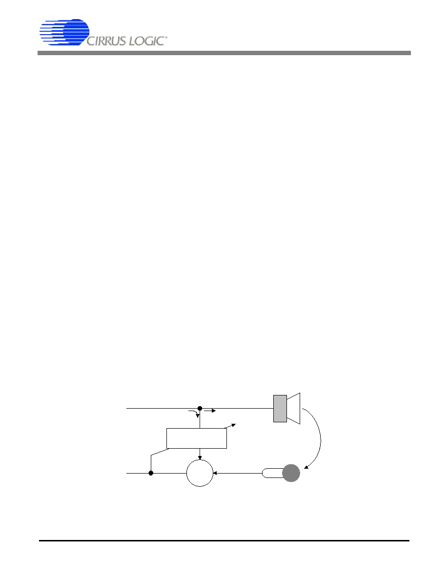
CS6422
32
4. DESIGN CONSIDERATIONS
When designing the CS6422 into a system, it is im-
portant to keep several considerations in mind.
These concerns can be loosely grouped into three
categories: algorithmic considerations, circuit de-
sign considerations, and system design consider-
ations.
4.1
Algorithmic Considerations
The CS6422 facilitates full-duplex hands-free
communication via many algorithms running on
the Digital Signal Processor that is the core of the
CS6422. Among these are the algorithms that per-
form the adaptive filtering, the half-duplex switch-
ing, digital volume control, and supplementary
echo suppression.
4.1.1
Full-Duplex Mode
Full-duplex hands-free communication is achieved
through a technique called adaptive filtering. The
basic principle behind adaptive filtering is that the
acoustic path between speaker and microphone can
be modeled by a transfer function which can be dy-
namically determined by an adaptive digital filter.
This principle assumes good update control and
speech/tone detection algorithms to prevent the fil-
ter from mistraining.
4.1.1.1
Theory of Operation
Figure 10 illustrates how the adaptive filter can
cancel echo and reduce loop gain. The echo path of
the system is between points B and C: the speaker
to microphone coupling. A signal injected at A
(sometimes called a "training signal") is sent both
to B, the input of the echo path, and to F, the input
of the adaptive filter. The signal at B is modified by
the acoustic transducers (speaker and microphone)
and the environment, and received at point C (as an
"Echo"). Meanwhile, assume that the adaptive fil-
ter has exactly the right transfer function to match
the echo path BC, and so the signal at point D is ap-
proximately equal to the signal at point C. After
these are subtracted by the summing element, all
that is left is the error signal at point E, which
should be very small.
If a person were to speak into the microphone at
point C, that signal would pass through the sum-
ming element unchanged because the adaptive fil-
ter had no comparable input to subtract out. In this
manner, the person at A and the person at C may si-
multaneously speak and A will not hear his own
echo.
In the real world, the echo path is not static. It will
change, for example, when people move in the
Adaptive Filter
A
E
D
B
C
+
-
F
Figure 10. Simplified Acoustic Echo Canceller Block Diagram
CS6422
32
DS295F1

CS6422
33
room, when someone moves the speaker or the mi-
crophone, or when someone drops a piece of paper
on top of the speaker. So, the filter needs to adapt
to modify its transfer function to match that of the
environment. It does so by measuring the error sig-
nal at point E and trying to minimize it. This signal
is fed back to the adaptive filter to measure perfor-
mance and how best to adapt, or train.
The trouble arises when the person at the near-end
(C) speaks: the error signal will be non-zero, but
the adaptive filter should not change. If it tries to
train to the near-end signal, the adaptive filter has
no way to reduce the error signal, because there is
no input to the filter, and therefore no output from
it. The adaptive filter would mistrain.
To prevent this mistraining, the echo canceller uses
double-talk detection algorithms to determine
when to update. These update control algorithms
are the heart of most echo canceller implementa-
tions.
The worst case situation for the CS6422 is when
parties at both ends are speaking and the person at
the near-end is moving. In this case, the echo can-
celler will cease to adapt because of the double-
talk, but the echo will not be optimally reduced be-
cause of the change in path.
4.1.1.2
Adaptive Filter
The adaptive filter in the CS6422 uses an algorithm
called the "Normalized Least-Mean-Square
(NLMS)" update algorithm to learn the echo path
transfer function. This Finite Impulse Response
(FIR) filter has 508 taps, which can model up to
63.5 ms of total path response at a sampling rate of
8kHz. The coverage time is calculated by the fol-
lowing formula:
x 508 = 63.5 ms.
The CS6422's adaptive filter, like all FIR filters,
only models Linear and Time Invariant (LTI) sys-
tems. So, any non-linearity in the echo path can not
be modeled by the adaptive filter and the resulting
signals will not be cancelled. Signal clipping and
poor-quality speakers are very common sources of
non-linearity and distortion.
A common integration problem for echo cancellers
is signal clipping in the echo path. For example, if
a speaker driver is driven to its rails, the distortion
of the speech may be hard to perceive, but it is very
bad for the echo canceller. The technique of over-
driving the speaker has been used in half-duplex
phones to provide good low-level signal gain at the
expense of distortion with high amplitude signals.
Since this does not work for the CS6422, an AGC
mechanism has been introduced to provide equiva-
lent behavior without clipping. See Section 4.1.3,
"AGC" for more details.
Another common problem is speaker quality. A
poor quality speaker which is perfectly acceptable
for a half-duplex speakerphone, may limit the echo
canceller's performance in a full-duplex speaker-
phone. The distortion elements are not modeled by
the adaptive filter and so limit its effectiveness.
Speakers should have better than 2% THD perfor-
mance to not impede the adaptive filter.
Volume control should be implemented using the
CS6422 Microcontroller Interface. A real-time ex-
ternal change in the gain of the speaker driver re-
sults in a change in the transfer function of the echo
path, and will force the adaptive filter to readapt. If
the volume control is done before the input to the
adaptive filter, the echo path does not change, and
retraining is not necessary. Another side benefit of
the CS6422 volume control is that it transparently
provides dynamic range compression through the
AGC function.
4.1.1.2.1 Pre-Emphasis
The typical training signal for the adaptive filter is
speech, but most adaptive filters train optimally
with white noise. Speech has very different spectral
1
8kHz
-------------
CS6422
DS295F1
33

CS6422
34
characteristics than white noise because of its qua-
si-periodic nature.
Research at Crystal has shown that quasi-periodic
signals cause the formation of spurious non-zero
coefficients within the adaptive filter at tap inter-
vals determined by the periodicity of the signal.
This results in small changes in period being very
destructive to the adaptive filter's performance.
One mechanism the CS6422 uses to prevent this
filter corruption with speech is to pre-emphasize
the signal sent to the adaptive filter so that much of
the low frequency content is removed.
The CS6422 works very well with a speech training
signal because of the pre-emphasis filter. White
noise training signals, however, result in sub-opti-
mal performance, so when testing with white noise,
it is recommended that the pre-emphasis filters be
disabled.
4.1.1.2.2 Graded Beta
The update gain of an adaptive filter, sometimes
called the "beta", is the rate at which the filter co-
efficients can change. If beta is too low, the adap-
tive filter will be slow to adapt. Conversely, if it is
too high, the filter will be unstable and will create
unwanted noise in the system.
In most echo canceller implementations, the beta is
a fixed value for all the filter coefficients. In some
situations, though, through knowledge of the char-
acteristics of echo path response, the beta can be
varied for groups of coefficients. This preserves
stability by allowing the beta to be higher for some
coefficients and compensating by reducing beta be-
low nominal for others.
For example, acoustic echo tends to decay expo-
nentially, so the first taps need to be larger than the
later taps. Having a beta profile that matches the
expected response path enhances the echo cancel-
ler's ability to correctly and accurately model the
acoustic path. Furthermore, this has an added ben-
efit of suppressing the spurious taps mentioned in
Section 4.1.1.2.1, "Pre-Emphasis".
The Microcontroller Interface allows four settings
for graded beta: none, 0.19 dB/ms, 0.38 dB/ms,
and 0.75 dB/ms. Use 0.75 dB/ms for acoustically
dead rooms or cars, and 0.19 dB/ms or no grading
of beta for large, or acoustically live rooms.
4.1.1.3
Update Control
As mentioned in Section 4.1.1.1, "Theory of Oper-
ation", the update control algorithms are the heart
of any useful echo canceller implementation. Aside
from telling the adaptive filter when to adapt, they
are responsible for correcting performance when
the path changes more quickly than the filter can
respond. For example, if the adaptive filter is actu-
ally adding signal power instead of cancelling it,
the update control algorithms will reset the adap-
tive filter to cleared coefficients, forcing it to re-
start.
4.1.1.4
Speech Detection
The CS6422 detects speech by using power estima-
tors to track deviations from a background noise
power level. The power estimators filter and aver-
age the raw incoming samples from the ADC.
A background noise level is established by a regis-
ter that increases 3 dB at intervals determined by
NseRmp (Register 2, bits 11 and 10). When the
power estimator level rises, the background noise
level will slowly increase to try to match it. When
the power estimator level is below the background
noise level, the background noise level adjusts
quickly to match the power estimator level. This
method allows significant flexibility in tracking the
background noise level.
Speech is detected when the power estimator level
rises above the background noise level by a given
threshold. The half-duplex receive speech detector
threshold is set by RHDet (Register 2, bits 15 and
14), the half-duplex transmit speech detector
threshold is set by THDet (Register 1, bits 15 and
CS6422
34
DS295F1

CS6422
35
14), and the receive suppression speech detector
threshold is set by RSThd (Register 2, bits 13 and
12). The transmit speech detectors for both half-du-
plex and suppression default to 6 dB.
Note that constant power signals which persist for
long durations, such as tones or white noise from a
signal generator, will be detected as speech only as
long as the background noise level has not risen to
within the speech detection threshold of the signal
power. When a tone has persisted for long enough,
the background noise level will be equal to the
power estimator level, and so the tone will no long-
er be considered speech. This duration is dependent
upon the power difference between the signal and
the ambient noise power, as well as NseRmp. It
should be noted that the CS6422 has a tone detector
to prevent updates when tones are present and allow
tones to persist regardless of the speech detectors.
4.1.2
Half-Duplex Mode
In cases where the system relies on the echo cancel-
ler for stability, a fail-safe mechanism must be in
place for instances when the echo canceller is not
performing adequately. The CS6422 implements a
half-duplex mode to guarantee communication
even when the echo canceller is disabled.
When the CS6422 is first powered on, or emerges
from a reset, the echo canceller coefficients are
cleared, and the echo cancellers provide no benefit
at this point. The half-duplex mode is on to prevent
howling and echo from interfering with communi-
cation. Once the CS6422's adaptive filters have
adapted sufficiently, the half-duplex mode is auto-
matically disabled, and full-duplex communication
can occur.
The half-duplex mode allows three states: <Trans-
mit>, <Receive>, and <Idle>. In the <Transmit>
state, the transmit channel is open and the receive
channel is muted. The <Receive> state mutes the
transmit channel. The <Idle> state is an internal
state which is used to enhance switching decision
making. The CS6422 must be <Idle> before it will
allow a state change between <Transmit> and <Re-
ceive>.
The half-duplex controller can be susceptible to
echo, so a holdover timer is provided to help pre-
vent false switching. Holdover will force the chan-
nel to remain in its current state for a fixed duration
after speech has stopped. HDly (Register 2, bits 9
and 8) sets the duration of the holdover. Longer
holdover will tend to make interrupting more diffi-
cult, but will be more robust to spurious switching
caused by echo.
4.1.2.1
Idle Return to Transmit
When enabled, this feature causes the CS6422 to
return to <Transmit> mode from an <Idle> state
when operating in half-duplex. This simulates
full-duplex-like behavior during the periods of
half-duplex operation at the beginning of a call.
4.1.3
AGC
The CS6422 implements a peak-limiting AGC in
both the transmit and receive directions in order to
boost low-level signals without compromising per-
formance when high amplitude signals are present.
The technique effectively results in dynamic range
compression.
The AGC works by setting a reference level based
on the value represented by TVol (Register 1, bits
11-8) for the transmit direction and RVol (Register
0, bits 11-8) for the receive direction. If the signal
from the input is above this reference, it is attenu-
ated to the reference level with an attack time of
125
�s. This attenuation level decays with a time
constant of 30 ms unless another signal greater than
the reference level is detected. After the attenua-
tion, a post-scaler scales the reference level to full-
scale (the maximum digital code), which amplifies
all signals by the difference between the reference
level and full-scale.
For example, Figure 11 shows how the AGC works
with a reference level of +30 dB (Word = 0000).
CS6422
DS295F1
35

CS6422
36
Any signal greater than 30 dB below full-scale (a),
is scaled down to 30 dB (b). This signal is then
scaled up +30 dB (the reference level) to provide
the final output (c). Note that the combination of at-
tenuation and gain results in less than +30 dB total
gain being applied. If the input signal is below
30 dB below full-scale (d), no attenuation is added
and the full +30 dB of gain is applied to the signal
(e).
When the reference level is set to +0 dB, the AGC
is effectively disabled. Volume control is imple-
mented by digital attenuation in 3 dB steps from
this point on down. The maximum gain is +30 dB,
and the minimum is -12 dB in 3 dB steps. The low-
est gain setting (1111) mutes the signal path. The
signal scaling takes place in between the two can-
cellers, and so does not disturb the echo canceller
as changing gain in the echo path, for example at
the speaker driver, would (see Section 4.1.1.2,
"Adaptive Filter" for more details).
4.1.4
Suppression
Echo cancellation is somewhat of a misnomer in
that echo is merely attenuated, not entirely can-
celled. Some residual echo still exists after the
summing node. This residual echo, though low in
amplitude, may be audible when the near-end talk-
er is not speaking. Suppression further attenuates
the echoed signal, preventing the far-end listener
from hearing echo.
The CS6422 employs supplementary echo suppres-
sion which adds attenuation on top of the cancella-
tion to remove the residual echo. For example, the
CS6422 will engage extra attenuation in the trans-
mit path whenever only the far-end talker is speak-
ing. However, if the near-end talker starts speaking,
this attenuation is removed and the system relies on
the near-end talker's speech to mask the residual
echo.
-30dB
Fs
(a) Input Signal
t
-30dB
Fs
(c) AGC Gain
t
-30dB
Fs
(b) AGC Attenuation
t
-30dB
Fs
(d) Input Signal
t
-30dB
Fs
(e) AGC Gain
t
0dB
0dB
0dB
0dB
0dB
Figure 11. How the AGC works (TVol = +30 dB)
CS6422
36
DS295F1

CS6422
37
Suppression may cause some modulation of the
perceived background noise which may be distract-
ing to some users. As a result, it may be desirable
to limit the suppression attenuation to the minimum
necessary. The CS6422 provides TSAtt (Register
3, bits 15 and 14) to control the amount of attenua-
tion introduced by suppression in the transmit
channel. Receive suppression attenuates by 24 dB.
4.1.4.1
Transmit Suppression
When TSMde = `1' (Noise Guard `off'), the trans-
mit suppressor attenuates the transmit path when
only far-end speech is present. When TSMde = `0'
(Noise Guard `on'), the suppressor attenuates when
the transmit channel is idle, that is, when no near-
end speech is present.
The purpose of Transmit Suppression is to mask re-
sidual echo by inserting additional loss/attenuation
in the transmit path in the scenario when far-end
speech is present; the residual echo, if any, in dou-
ble-talk is masked by near-end speech, assuming
reasonable levels of ERLE.
There are four controls that govern the behavior of
Transmit Suppression. These are TSThd (Register
3, bits 7 and 6), TSAtt (Register 3, bits 15 and 14),
TSBias (Register 3, bits 5 and 4), and TSMde (Reg-
ister 0, bit 4). TSThd is the primary control and
should be adjusted before changing the value of
TSBias from its default setting. TSThd sets the
ERLE expectation to be used in discriminating be-
tween near-end speech and far-end echo. This con-
trol setting will by far predominate in affecting the
manner in which Transmit Suppression behaves.
TSAtt controls the amount of attenuation added to
the transmit path when the transmit suppressor en-
gages.
TSBias is a secondary control. This is to be adjust-
ed after the system designer is more or less satisfied
with the behavior of Transmit Suppression with the
TSThd set. It affects the ease with which a near-end
talker may disengage Transmit Suppression and
keep it disengaged. We recommend using larger
values of TSBias relative to TSThd settings in or-
der to facilitate ease of near-end speech transmis-
sion. For example, the default setting for TSThd is
15 dB and 18 dB for TSBias.
In some scenarios, especially when the dynamic
range of volume control is significantly large, we
also recommend the use of different combinations
of TSThd and TSBias setting relative to output vol-
ume of the acoustic interface. Specifically, higher
volume levels may call for larger values of TSThd.
TSMde controls the Noise Guard feature. When
TSMde = `0' (Noise Guard enabled), the transmit
suppressor is engaged when no near-end speech is
present. When TSMde = `1' (Noise Guard dis-
abled), the transmit suppressor is engaged only
when far-end speech is present in the absence of
near-end speech.
4.1.4.2
Receive Suppression
The receive suppressor is nominally attenuating
unless far-end speech is present. This behavior is
more consistent with behavior observed in modern
speakerphones, and helps keep noise levels low.
One side effect of this scheme is that a constant
power signal, such as noise from a noise generator
or a tone, will eventually be attenuated when the
background noise level estimate turns off the re-
ceive suppression speech detector. See Section
4.1.1.4, "Speech Detection" from more details.
RSThd (Register 2, bits 13 and 12) sets the speech
detection threshold of the suppressor's speech de-
tector. This control is normally set to the same val-
ue as RHDet. See Section 4.1.1.4, "Speech
Detection" for more details.
4.1.4.3
Double-talk Attenuation
In full-duplex hands-free to full-duplex hands-free
scenarios (where a call exists between two full-du-
plex speakerphones), stability problems can arise at
higher volume levels due to the acoustic coupling
CS6422
DS295F1
37

CS6422
38
loop (near-end speaker/mic to far-end speaker/mic)
during a double-talk scenario (where both near-end
and far-end parties are talking at the same time).
The CS6422 implements an optional attenuation
feature that introduces a programmable amount of
loss in the transmit and/or receive directions dur-
ing double-talk to alleviate stability concerns with-
out sacrificing speaker volume. This allows for
higher speaker volume levels at both ends of the
call without compromising stability.
4.1.4.4
Noise Guard
Noise Guard is an optional noise squelch feature
that operates in the transmit path (near-end micro-
phone to far-end speaker). In traditional systems, if
the near-end talker is located in a noisy environ-
ment, the near-end system will remain in transmit
mode and transmit that noise to the far-end listener.
While this may be bothersome to the far-end listen-
er using a standard handset, this creates a real prob-
lem if the listener is using a traditional half-duplex
speakerphone because the far-end phone may stay
in receive mode and not allow the far-end talker to
be heard. Noise guard eliminates this problem by
squelching the transmit channel at the near-end un-
less near-end speech is detected, permitting the far-
end speakerphone to switch normally during the
conversation.
4.2
Circuit Design
The design of the CS6422 interface circuitry plays
an important role in achieving optimum perfor-
mance. The actual circuit design is important, espe-
cially the analog interface. Proper grounding and
layout will help minimize the noise that might get
coupled into the CS6422.
4.2.1
Interface Considerations
Of the CS6422 interfaces, the analog interface and
the microcontroller interface are the most impor-
tant to pay special attention to during circuit de-
sign. The analog interface especially will
determine how well the echo canceller can per-
form.
4.2.1.1
Analog Interface
The Analog Interface feeds information about the
echo path to the adaptive filter, so it is critical that
this interface be well designed. Using high-quality
transducers and circuits that guarantee low-distor-
tion and minimal clipping are essential to the suc-
cess of any echo canceller based design.
As mentioned in Section 4.1.1.2, "Adaptive Filter",
the adaptive filter assumes that the echo path is lin-
ear and time-invariant. As such, poor quality
speakers are a common cause of poor echo cancel-
ler performance due to their high distortion. Speak-
ers must be selected with their linearity in mind. In
general, the speaker should have less than 2% Total
Harmonic Distortion (THD). This will result in dis-
tortion terms 34 dB below the desired signal,
enough headroom for the echo canceller to function
adequately.
The other major consideration in the design of the
analog interface is that the circuitry that processes
the transducer signals not clip or distort it. For ex-
ample, a common problem is the use of a speaker
amplifier with a fixed gain, which clips when driv-
ing the speaker. Although the distortion may not be
objectionable to the human ear, it will prevent the
adaptive filter from modeling the path correctly.
Speakers and microphones which worked for half-
duplex speakerphones will not necessarily work for
full-duplex speakerphones. Microphone amplifier
circuitry is also suspect when looking for sources
of clipping and distortion.
4.2.1.2
Microcontroller Interface
The Microcontroller Interface is the only asynchro-
nous digital connection to the CS6422, so it is the
most likely place for digital noise coupling to be a
problem. The interface itself is fairly straightfor-
ward and requires only three pins from a microcon-
troller.
CS6422
38
DS295F1

CS6422
39
The three pins that comprise the Microcontroller
Interface are STROBE, DATA, and DRDY. Also,
four extra clocks are required after DRDY is
brought high in order to latch the data into the
CS6422, as is shown in Figure 7.
4.2.2
Grounding Considerations
Proper grounding of the CS6422 is necessary for
optimal performance from this mixed-signal de-
vice. The CS6422 should be considered an analog
device for grounding purposes.
The digital sections of the CS6422 are synchro-
nized with its ADCs and DACs to minimize the ef-
fects of digital noise coupling. However, for
external digital devices that are asynchronous with
respect to the CS6422, precautions should be taken
to minimize the chances of digital noise coupling
into the CS6422.
A design with the CS6422 should have a separate
ground plane for any digital devices. For example,
a system microcontroller should be on a digital
ground plane with its control lines leading to the
CS6422 in the shortest reasonable distance. The
CS6422 itself should lie completely on the analog
ground plane.
4.2.3
Layout Considerations
The physical layout of the traces and components
around the CS6422 will also strongly affect the per-
formance of the device. Special attention must be
paid to decoupling capacitors, the crystal oscillator,
and the input anti-aliasing filters.
The decoupling capacitors for the power supplies
of the CS6422 should be placed as close as possible
to the power pins for best performance. There are
two capacitors per pin: the 0.1
�F capacitor needs
to be closest to the pin to decouple the high fre-
quency components, and the larger cap can be far-
ther away. The MB pin is the most critical as it
connects directly to the on-chip voltage reference.
AVDD and DVDD are secondary to MB with re-
spect to priority.
The crystal oscillator should be placed as close as
possible to reduce the distance that the high fre-
quency signals must travel. If the crystal is placed
too far away, the trace inductance may cause prob-
lems with oscillator startup.
The next concern with placement is the input anti-
aliasing filters for the ADC inputs. NI has an RC
low-pass network with a corner frequency of
8 kHz. The capacitor of this low-pass network
should be placed very close to the pin so that there
is very little exposed trace to pick up noise. If the
on-chip microphone amplifier is used, the 0.022
�F
capacitor on APO will provide the appropriate cut-
off frequency, and so should be placed close to the
APO pin. If the on-board preamplifier is not used,
APO will have the same RC network as NI, and
should be treated similarly.
The connections from the controller to the Micro-
controller Interface should be short straight traces,
if possible. The traces should not run very close to
any digital clocks to avoid cross coupling.
4.3
System Design
The CS6422 is ultimately only one part of a bigger
full-duplex hands-free system. In order for that sys-
tem to work well, it needs to be properly balanced.
The distribution of the system gains will make or
break the echo canceller. In order to judge perfor-
mance, however, the system integrator must be
armed with the means to test the product.
4.3.1
Gain Structure
The distribution of the system gains is an important
design consideration to keep in mind. Gain distri-
bution is an intricate balancing act where the sys-
tem integrator tries to maximize dynamic range
while minimizing noise, and at the same time, get-
ting excellent echo canceller performance.
The basic constraint on getting good echo canceller
performance is that the maximum output should
not clip when coupled to the input. For example, if
in a speakerphone, AO provides 1.1 V
rms
to a
CS6422
DS295F1
39

CS6422
40
speaker, the reflections reaching the microphone
should present no more than 0.9 V
rms
to the Acous-
tic ADC. In fact, it is advisable to allow 6 dB or
even 12 dB of margin, such that in the above exam-
ple, the signal present at the Acoustic ADC is
250 mV
rms
.
After this coupling level is established, the desired
signal gain must be established. To continue from
the previous example, the transmit gain must be ad-
justed to make sure the near-end talker is easy to
hear at the far-end. If the signal from the near-end
talker clips at the ADC, it is not significant to the
echo path because the AEC should not be updating
anyway.
In general, to minimize noise system gain should
be concentrated before the ADC. However, this is
not practical in all cases, mostly because of the cou-
pling constraint. The CS6422 offers the AGC'd
gains provided by TVol and RVol to help provide
the desired transmit and receive gains.
The CS6422 offers two different programmable
gain sources: TGain/RGain and TVol/RVol. TGain
and RGain provide analog gain at the input to the
ADC of 0 dB, 6 dB, 9.5 dB, or 12 dB. TVol and
RVol introduce digital gain and attenuation in 3 dB
steps. The difference is significant in that the digital
gain will gain up the noise of the ADC as well as the
desired signal, whereas the analog gain will not.
Furthermore, gains introduced by TVol and RVol
will not result in clipping, since both gains are
AGC'ed, unlike the gains at TGain and RGain
which are not.
4.3.2
Testing Issues
The following tests are suggestions for measuring
echo canceller and half-duplex performance.
4.3.2.1
ERLE
Echo Return-Loss Enhancement (ERLE) is a mea-
sure of the attenuation that an echo canceller pro-
vides. The number is an expression of the ratio of
the level of signal without the echo canceller com-
pared to the level of signal with the echo canceller.
When measuring ERLE, it is important that any po-
tential signal loops be broken; so to measure the
ERLE of the Acoustic Canceller, the NO output
should be disconnected from the rest of the net-
work. This will prevent feedback which could oc-
cur when all of the CS6422's failsafes are disabled.
The following example outlines the steps necessary
to measure the ERLE of the acoustic echo cancel-
ler.
It is important to choose a good test signal for the
tests to be valid. As mentioned in Section 4.1.1.2,
"Adaptive Filter", the CS6422 does not work opti-
mally with white noise. The best signal to use
would be a repeatable speech signal, like a record-
ing of someone counting or saying "ah."
Use the Microcontroller Interface to disable trans-
mit and receive suppression, half-duplex, and the
Network Echo Canceller. The gains should be set
appropriate for good system performance.
The first measurement is a baseline figure of per-
formance with no echo canceller. Use the Micro-
controller Interface to clear the acoustic canceller
coefficients. Inject the test signal at NI and measure
the rms voltage at NO. This measurement gives the
baseline coupling level (denominator).
Use the Microcontroller Interface to set the acous-
tic canceller coefficients to normal which will al-
low the adaptive filter to adapt. Inject the test signal
at NI and allow a few seconds for the filter to adapt.
Again, measure the rms voltage at NO. This mea-
surement gives the cancelled echo level (numera-
tor).
Convert both voltages to decibels and subtract the
echo cancelled level from the baseline level to cal-
culate the ERLE. At the factory, with known good
components, we typically see 30 dB of ERLE with
speech.
CS6422
40
DS295F1

CS6422
41
4.3.2.2
Convergence Time
Convergence time is a measure of how quickly the
adaptive filter can model the echo path. From
cleared coefficients, the training signal is injected
into the echo canceller and the time for the ERLE
to reach a given threshold value is the convergence
time. Different customers will have different
threshold levels, so Crystal does not specify con-
vergence time.
The following example will measure convergence
time for the acoustic echo canceller:
Set up the system as for the ERLE test. Clear the
acoustic canceller coefficients through the Micro-
controller Interface. Apply the training signal to
NI, set the coefficients to normal, and simulta-
neously start a timer. Once the measured ERLE
reaches the threshold the system designer desires,
stop the timer. The elapsed time is the convergence
time. A good value for the threshold would be the
AErle value from Register 3, since this would be
the time for the CS6422 to go from half-duplex
mode to full-duplex mode.
A good tool for this measurement is a digital stor-
age oscilloscope set to a slow sweep so that about
five seconds of signal is shown on the screen. One
channel of the oscilloscope should monitor the
ADC input (for an uncancelled reference), and an-
other channel should monitor the echo cancelled
output. This technique is especially effective when
speech is the training signal.
We see about 2-5 seconds of training time using
known good equipment. This time assumes contin-
uous speech as the training signal. Pauses will ex-
tend the convergence time.
4.3.2.3
Half-Duplex Switching
Although the CS6422 transitions from half-duplex
to full-duplex operation from reset after only a few
utterances are passed through the system, the per-
formance of half-duplex is critical to the end-user
in cases where the echo canceller is not adequate.
The half-duplex switching characteristics can be
subjectively tested with the following procedure:
Set the CS6422 Microcontroller Interface to the
nominal register values for the system, but clear the
acoustic and network echo canceller coefficients.
This will force the CS6422 to remain in half-duplex
mode.
The most useful test of practical performance
found at Crystal has been the "alternating counting
test." In this test the person at the near-end counts
all the odd numbers and the person at the far-end
counts all the even numbers. This tests the inter-
ruptibility of the half-duplexer. During testing, sys-
tem parameters for the half-duplex may need to be
changed to accommodate the level of performance
expected for the product. See Section 4.1.2, "Half-
Duplex Mode" and Section 3.2.2, "Register Defini-
tions"for more details.
CS6422
DS295F1
41

CS6422
42
5. PIN DESCRIPTIONS
Analog Interface
AO - Acoustic Interface Output, Pin 3
Analog voltage output for the acoustic side (near-end output/receive output). Maximum output signal is
1.1 V
rms
(3.1 V
pp
). This output can drive down to 10 k
and is usually followed by a speaker driver. The
output is pre-compensated to expect a single-pole RC low pass filter with a corner frequency of 4 kHz.
NO - Network Interface Output, Pin 4
Analog voltage output for the network side (far-end output/transmit output). Maximum output signal is
1.1 V
rms
(3.1 V
pp
). This output can drive down to 10 k
. The output is pre-compensated to expect a
single-pole RC low pass filter with a corner frequency of 4 kHz.
API - Acoustic Interface Preamplifier Input, Pin 20
Input to the acoustic side microphone preamplifier. Signal source resistance at this pin will reduce the
34 dB gain inherent in the preamplifier. The maximum input signal level to avoid clipping is 20 mV
rms
(57 mV
pp
), assuming default settings.
APO - Acoustic Interface Preamplifier Output, Pin 18
Output of the acoustic side microphone preamplifier and input to the acoustic side analog-to-digital
converter (near-end input/transmit input). This input expects a single-pole RC anti-aliasing filter with a
corner frequency of 8 kHz. Maximum signal level before clipping at this point is 0.9 V
rms
(2.5 V
pp
),
assuming default settings for TGain.
MB - Microphone Bias Voltage Output, Pin 19
Output of 3.5 VDC provides the internal voltage reference for the CS6422. MB must be decoupled with
a 10
�F and 0.1 �F capacitor to prevent noise from affecting the on-chip voltage reference. MB must
not be connected to any load.
1
2
3
4
5
6
7
8
12
13
14
15
16
AVDD
AGND
AO
NO
RST
DRDY
STROBE
DATA
DVDD
DGND
CLKI
CLKO
NC4
9
10
NC1
NC2
17
18
APO
NI
19
20
API
MB
11
NC3
CS6422
CS6422
42
DS295F1

CS6422
43
NI - Network Interface Input, Pin 17
Input to the network side analog-to-digital converter (far-end input/receive input). This input expects a
single-pole RC anti-aliasing filter with a corner frequency of 8 kHz. Maximum signal level before clipping
at this point is 0.9 V
rms
(2.5 V
pp
), assuming default settings for RGain.
Microcontroller Interface
RST - Active Low Reset Input, Pin 5
When RST is held low, the CS6422 is put into a low power mode with all functional blocks idle. When
RST goes high, the CS6422 is started in a known state.
DRDY - Active Low Microcontroller Interface Data Ready Input, Pin 6
DRDY is a low pulse used to gate valid input data into the Microcontroller Interface.
STROBE - Microcontroller Interface Clock Input, Pin 7
The rising edge of STROBE latches DATA into the Microcontroller Interface while DRDY is low.
DATA - Microcontroller Interface Data Input, Pin 8
DATA is latched into the Microcontroller Interface on the rising edge of STROBE.
Clock
CLKI - Clock Oscillator Input, Pin 14
A 20.480 MHz parallel-resonant crystal should be connected between CLKI and CLKO. Alternatively,
CLKI may be driven directly with an 20.480 MHz CMOS level clock.
CLKO - Clock Oscillator Output, Pin 13
A 20.480 MHz parallel-resonant crystal should be connected between CLKI and CLKO. CLKO must be
left floating if CLKI is driven directly with a CMOS level clock.
Power Supply
AVDD - Analog Supply, Pin 1
+5 Volt analog power supply.
AGND - Analog Ground, Pin 2
Analog ground reference.
DVDD - Digital Supply, Pin 16
+5 Volt digital power supply.
DGND - Digital Ground, Pin 15
Digital ground reference.
CS6422
DS295F1
43

CS6422
44
Miscellaneous
NC1 - No Connect, Pin 9
Must be floating for normal operation.
NC2 - No Connect, Pin 10
Must be floating for normal operation.
NC3 - No Connect, Pin 11
Must be floating for normal operation.
NC4 - No Connect, Pin 12
Must be floating for normal operation.
CS6422
44
DS295F1

CS6422
45
6. GLOSSARY
Echo
A signal that returns to its source after some delay.
Network Echo
Echo resulting from signal reflection due to an impedance mismatch in a 2-to-4 wire converter (hybrid).
Acoustic Echo
Echo created by signal propagation in a room from a speaker to a microphone.
Reverberation
Local information that bounces around the room before it reaches the microphone. An example of
reverberation is when your back is to the speakerphone, and your voice bounces off the wall before it
reaches the microphone.
Near-End
The location with the acoustic interface (speaker and microphone).
Far-End
The location connected to the network interface.
Transmit Path
The signal path from Near-End input to Far-End output.
Receive Path
The signal path from Far-End input to Near-End output.
Full-Duplex
The state when both Transmit and Receive paths are simultaneously active.
Half-Duplex
The state when either Transmit or Receive path is active.
Supplementary Echo Suppression
Dynamic attenuation placed in the opposite path of the active path to mask residual echo. For example,
if the receive path is active, the transmit path is attenuated. When both paths are simultaneously active,
the suppression attenuation is removed. See Section 4.1.4, "Suppression" for more details.
Howling
In full-duplex operation, both the microphone and speaker are active at the same time, which, in
conjunction with the reflection off the hybrid, creates a closed loop. The signal coupling between the
speaker and the microphone can cause feedback oscillation or howling. This happens when the
coupling between the speaker and microphone is strong enough to increase the system's closed loop
gain above unity.
Acoustic Coupling
The strength of the output signal from the speaker that is received at the microphone input.
CS6422
DS295F1
45

CS6422
46
Adaptive Filter
A digital FIR filter that adjusts its coefficients to match a transfer function, such as the echo path
between the speaker and microphone. The adaptive filter is able to compensate for different and
changing conditions, such as someone moving in the room.
Echo Path
The acoustic echo path describes the acoustic coupling between the speaker and the microphone. It
describes both the magnitude and delay characteristics of the echoed signal. It is affected by the
speaker, microphone, phone housing, room, objects in the room, movement, and the talker. The
network echo path is comprised of the transfer function between NO and NI.
Path Change
A change in the transfer function that describes the Echo Path. Changes in the acoustic echo path are
most commonly due to motion in the room or gain changes at an external speaker. Network echo path
is most easily changed by picking up an extension or hanging up the phone.
AGC
The CS6422 implements a peak-limiting Automatic Gain Control to allow a greater dynamic range
without clipping the signal. See Section 4.1.3, "AGC" for details on how it works.
Doubletalk
The condition occurring when both Near End and Far End talkers are speaking simultaneously.
ERLE
Echo Return-Loss Enhancement is the amount of attenuation of echo signal an echo canceller provides
(not counting Suppression) as measured in dB. ERLE is a measure of the echo canceller's
performance. The larger the value for ERLE, the better the echo cancellation.
Coverage Time
The CS6422 echo canceller has 508 taps and it can sample an analog signal at an 8 kHz rate.
512 x 1/8 kHz = 63.5 ms. Sound travels through air at a rate of around 1 ft/ms. Thus the echo canceller
can be used in a room with walls 32 feet away, discounting multiple reflections. But remember that at
this distance, most of the echo has been attenuated due to the physical separation. The majority of the
acoustic coupling comes from the first arrival, or directly from the speaker to the microphone. The first
signal is by far the strongest.
Convergence Time
A high quality echo canceller is continuously modifying its internal model of the echo path characteristics
(See Section 4.1.1.2, "Adaptive Filter"). When the model is complete, the echo canceller will be able to
cancel echo to the extent of its rated capabilities. Convergence time is the duration it takes the echo
canceller to train itself, from cleared coefficients, and switch to full-duplex operation, in the presence of
speech.
CS6422
46
DS295F1

CS6422
47
7. PACKAGE DIMENSIONS
INCHES
MILLIMETERS
DIM
MIN
NOM
MAX
MIN
NOM
MAX
A 0.093
0.098
0.104
2.35
2.50
2.65
A1
0.004
0.008
0.012
0.10
0.20
0.30
b
0.013
0.017
0.020
0.33
0.43
0.51
C
0.009
0.011
0.013
0.23
0.28
0.32
D
0.496
0.504
0.512
12.60
12.80
13.00
E
0.291
0.295
0.299
7.40
7.50
7.60
e
0.040
0.050
0.060
1.02
1.27
1.52
H
0.394
0.407
0.419
10.00
10.34
10.65
L
0.016
0.025
0.050
0.40
0.64
1.27
0�
4�
8�
0�
4�
8�
JEDEC #: MS-013
Controlling Dimension is Inches/Chip Pac
Controlling Dimension is Millimeters/Jedec
20L SOIC (300 MIL BODY) PACKAGE DRAWING
D
H
E
b
A1
A
c
L
SEATING
PLANE
e
1
CS6422
DS295F1
47
CS6422
48
DS295F1
ORDERING INFORMATION
ENVIRONMENTAL, MANUFACTURING, & HANDLING INFORMATION
* MSL (Moisture Sensitivity Level) as specified by IPC/JEDEC J-STD-020.
REVISION HISTORY
Model
Temperature
Package
CS6422-CS
0 to +70 �C
20-pin SOIC
CS6422-CSZ (Lead Free)
CS6422-IS
-40 to +85 �C
CS6422-ISZ (Lead Free)
Model Number
Peak Reflow Temp
MSL Rating*
Max Floor Life
CS6422-CS
240 �C
2
365 Days
CS6422-CSZ (Lead Free)
260 �C
3
7 Days
CS6422-IS
240 �C
2
365 Days
CS6422-ISZ (Lead Free)
260 �C
3
7 Days
Revision
Date
Changes
PP4
JUL 2001
Preliminary Release
F1
SEP 2005
Updated device ordering info. Updated legal notice. Added MSL data..
Contacting Cirrus Logic Support
For all product questions and inquiries contact a Cirrus Logic Sales Representative.
To find the one nearest to you go to
www.cirrus.com
IMPORTANT NOTICE
Cirrus Logic, Inc. and its subsidiaries ("Cirrus") believe that the information contained in this document is accurate and reliable. However, the information is subject
to change without notice and is provided "AS IS" without warranty of any kind (express or implied). Customers are advised to obtain the latest version of relevant
information to verify, before placing orders, that information being relied on is current and complete. All products are sold subject to the terms and conditions of sale
supplied at the time of order acknowledgment, including those pertaining to warranty, indemnification, and limitation of liability. No responsibility is assumed by Cirrus
for the use of this information, including use of this information as the basis for manufacture or sale of any items, or for infringement of patents or other rights of third
parties. This document is the property of Cirrus and by furnishing this information, Cirrus grants no license, express or implied under any patents, mask work rights,
copyrights, trademarks, trade secrets or other intellectual property rights. Cirrus owns the copyrights associated with the information contained herein and gives con-
sent for copies to be made of the information only for use within your organization with respect to Cirrus integrated circuits or other products of Cirrus. This consent
does not extend to other copying such as copying for general distribution, advertising or promotional purposes, or for creating any work for resale.
CERTAIN APPLICATIONS USING SEMICONDUCTOR PRODUCTS MAY INVOLVE POTENTIAL RISKS OF DEATH, PERSONAL INJURY, OR SEVERE PROP-
ERTY OR ENVIRONMENTAL DAMAGE ("CRITICAL APPLICATIONS"). CIRRUS PRODUCTS ARE NOT DESIGNED, AUTHORIZED OR WARRANTED FOR USE
IN AIRCRAFT SYSTEMS, MILITARY APPLICATIONS, PRODUCTS SURGICALLY IMPLANTED INTO THE BODY, AUTOMOTIVE SAFETY OR SECURITY DE-
VICES, LIFE SUPPORT PRODUCTS OR OTHER CRITICAL APPLICATIONS. INCLUSION OF CIRRUS PRODUCTS IN SUCH APPLICATIONS IS UNDERSTOOD
TO BE FULLY AT THE CUSTOMER'S RISK AND CIRRUS DISCLAIMS AND MAKES NO WARRANTY, EXPRESS, STATUTORY OR IMPLIED, INCLUDING THE
IMPLIED WARRANTIES OF MERCHANTABILITY AND FITNESS FOR PARTICULAR PURPOSE, WITH REGARD TO ANY CIRRUS PRODUCT THAT IS USED
IN SUCH A MANNER. IF THE CUSTOMER OR CUSTOMER'S CUSTOMER USES OR PERMITS THE USE OF CIRRUS PRODUCTS IN CRITICAL APPLICA-
TIONS, CUSTOMER AGREES, BY SUCH USE, TO FULLY INDEMNIFY CIRRUS, ITS OFFICERS, DIRECTORS, EMPLOYEES, DISTRIBUTORS AND OTHER
AGENTS FROM ANY AND ALL LIABILITY, INCLUDING ATTORNEYS' FEES AND COSTS, THAT MAY RESULT FROM OR ARISE IN CONNECTION WITH
THESE USES.
Cirrus Logic, Cirrus, and the Cirrus Logic logo designs are trademarks of Cirrus Logic, Inc. All other brand and product names in this document may be trademarks
or service marks of their respective owners.