Preliminary Product Information
This document contains information for a new product.
Cirrus Logic reserves the right to modify this product without notice.
1
Copyright
Cirrus Logic, Inc. 2001
(All Rights Reserved)
P.O. Box 17847, Austin, Texas 78760
(512) 445 7222 FAX: (512) 445 7581
http://www.cirrus.com
Features
!
Single-Chip IEEE 802.3 Physical Interface IC
for 100BASE-TX, 100BASE-FX and
10BASE-T
!
Adaptive Equalizer provides Extended
Length Operation (>160 m) with Superior
Noise Immunity and NEXT Margin
!
Extremely Low Transmit Jitter (<400 ps)
!
Low Common Mode Noise on TX Driver for
Reduced EMI Problems
!
Integrated RX and TX Filters for 10BASE-T
!
Compensation for Back-to-Back "Killer
Packets"
!
Digital Interfaces Supported
� Media Independent Interface (MII) for
100BASE-X and 10BASE-T
� Repeater 5-bit code-group interface
(100BASE-X)
� 10BASE-T Serial Interface
!
Register Set Compatible with DP83840A
!
IEEE 802.3 Auto-Negotiation with Next Page
Support
!
Six LED drivers (LNK, COL, FDX, TX, RX,
and SPD)
!
Low power (135 mA Typ) CMOS design
operates on a single 5 V supply
Description
The CS8952 uses CMOS technology to deliver a high-
performance, low-cost 100BASE-X/10BASE-T Physical
Layer (PHY) line interface. It makes use of an adaptive
equalizer optimized for noise and near end crosstalk
(NEXT) immunity to extend receiver operation to cable
lengths exceeding 160 m. In addition, the transmit cir-
cuitry has been designed to provide extremely low
transmit jitter (<400 ps) for improved link partner perfor-
mance. Transmit driver common mode noise has been
minimized to reduce EMI for simplified FCC certification.
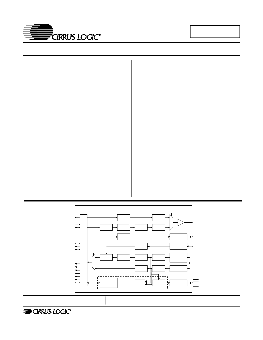
The CS8952 incorporates a standard Media Indepen-
dent Interface (MII) for easy connection to a variety of 10
and 100 Mb/s Media Access Controllers (MACs). The
CS8952 also includes a pseudo-ECL interface for use
with 100Base-FX fiber interconnect modules.
ORDERING INFORMATION
CS8952-CQ
0 to 70 �C
100-pin TQFP
CDB8952
Evaluation Board
TX_EN
TX_ER/TXD4
TXD[3:0]
TX_CLK
MDC
MII_IRQ
MDIO
CRS
COL
RX_ER/RXD4
RX_DV
RXD[3:0]
RX_CLK
RX_EN
TX+,
TX-
TX_NRZ+,
TX_NRZ-
RX_NRZ+,
RX_NRZ-
RX+,
RX-
LED1
LED2
LED3
LED4
LED5
10/100
M
U
X
4B/5B
Decoder
Descrambler
Manchester
Encoder
Scrambler
Fiber NRZI
Interface
MLT-3
Encoder
10BaseT
Filter
Slew Rate
Control
M
U
X
10/100
4B/5B
Encoder
ECL Driver
ECL Receiver
Adaptive Eq. &
Baseline Wander
Compensation
10BaseT
Filter
LED
Drivers
100BaseT
Slicer
10BaseT
Slicer
Fiber NRZI
Interface
MLT-3
Decoder
Manchester
Decoder
Auto
Negotiation
Timing
Recovery
MII
Control/Status
Registers
Link
Management
CS8952 10BaseT/100Base-X
Transceiver
M
edi
a
I
ndepen
dent
I
n
t
e
r
f
ac
e
(M
I
I
)
DS206PP3
OCT `01
CS8952
CrystalLANTM 100BASE-X and 10BASE-T Transceiver

CS8952
2
CrystalLANTM 100BASE-X and 10BASE-T Transceiver
TABLE OF CONTENTS
SPECIFICATIONS AND CHARACTERISTICS............................................................. 4
ABSOLUTE MAXIMUM RATINGS ....................................................................... 4
RECOMMENDED OPERATING CONDITIONS ................................................... 4
QUARTZ CRYSTAL REQUIREMENTS ............................................................... 4
DC CHARACTERISTICS ..................................................................................... 5
10BASE-T CHARACTERISTICS ......................................................................... 7
100BASE-X CHARACTERISTICS ....................................................................... 8
100BASE-TX MII RECEIVE TIMING - 4B/5B ALIGNED MODES ........................ 9
100BASE-TX MII RECEIVE TIMING - 5B BYPASS ALIGN MODE ................... 10
100BASE-TX MII TRANSMIT TIMING - 4B/5B ALIGN MODES ........................ 11
100BASE-TX MII TRANSMIT TIMING - 5B BYPASS ALIGN MODE ................ 12
10BASE-T MII RECEIVE TIMING ...................................................................... 13
10BASE-T MII TRANSMIT TIMING ................................................................... 14
10BASE-T SERIAL RECEIVE TIMING .............................................................. 15
10BASE-T SERIAL TRANSMIT TIMING ............................................................ 16
AUTO NEGOTIATION / FAST LINK PULSE TIMING ........................................ 17
SERIAL MANAGEMENT INTERFACE TIMING ................................................. 18
INTRODUCTION .......................................................................................................... 19
High Performance Analog ................................................................................... 19
Low Power Consumption .................................................................................... 19
Application Flexibility ........................................................................................... 19
Typical Connection Diagram ............................................................................... 19
FUNCTIONAL DESCRIPTION .................................................................................... 21
Major Operating Modes ....................................................................................... 21
100BASE-X MII Application (TX and FX) ..................................................... 21
Symbol Encoding and Decoding ........................................................... 22
100 Mb/s Loopback ............................................................................... 23
100BASE-X Repeater Application ............................................................... 23
10BASE-T MII Application ........................................................................... 24
Full and Half Duplex operation .............................................................. 24
Collision Detection ................................................................................. 24
Jabber ................................................................................................... 24
Link Pulses ............................................................................................ 24
Receiver Squelch .................................................................................. 25
10BASE-T Loopback ............................................................................. 25
Carrier Detection ................................................................................... 25
Contacting Cirrus Logic Support
For a complete listing of Direct Sales, Distributor, and Sales Representative contacts, visit the Cirrus Logic web site at:
http://www.cirrus.com/corporate/contacts/sales.cfm
Preliminary product information describes products which are in production, but for which full characterization data is not yet available. Advance product infor-
mation describes products which are in development and subject to development changes. Cirrus Logic, Inc. has made best efforts to ensure that the information
contained in this document is accurate and reliable. However, the information is subject to change without notice and is provided "AS IS" without warranty of
any kind (express or implied). Customers are advised to obtain the latest version of relevant information to verify, before placing orders, that information being
relied on is current and complete. All products are sold subject to the terms and conditions of sale supplied at the time of order acknowledgment, including those
pertaining to warranty, patent infringement, and limitation of liability. No responsibility is assumed by Cirrus Logic, Inc. for the use of this information, including
use of this information as the basis for manufacture or sale of any items, nor for infringements of patents or other rights of third parties. This document is the
property of Cirrus Logic, Inc. and by furnishing this information, Cirrus Logic, Inc. grants no license, express or implied under any patents, mask work rights,
copyrights, trademarks, trade secrets or other intellectual property rights of Cirrus Logic, Inc. Cirrus Logic, Inc., copyright owner of the information contained
herein, gives consent for copies to be made of the information only for use within your organization with respect to Cirrus Logic integrated circuits or other parts
of Cirrus Logic, Inc. The same consent is given for similar information contained on any Cirrus Logic website or disk. This consent does not extend to other
copying such as copying for general distribution, advertising or promotional purposes, or for creating any work for resale. The names of products of Cirrus Logic,
Inc. or other vendors and suppliers appearing in this document may be trademarks or service marks of their respective owners which may be registered in some
jurisdictions. A list of Cirrus Logic, Inc. trademarks and service marks can be found at http://www.cirrus.com
.

CS8952
CrystalLANTM 100BASE-X and 10BASE-T Transceiver
3
10BASE-T Serial Application ....................................................................... 25
Auto-Negotiation ................................................................................................. 25
Reset Operation .................................................................................................. 26
LED Indicators..................................................................................................... 26
MEDIA INDEPENDENT INTERFACE (MII) ................................................................. 27
MII Frame Structure ............................................................................................ 27
MII Receive Data................................................................................................. 28
MII Transmit Data................................................................................................ 28
MII Management Interface .................................................................................. 29
MII Management Frame Structure ...................................................................... 29
CONFIGURATION ...................................................................................................... 30
Configuration At Power-up/Reset Time............................................................... 30
Configuration Via Control Pins ............................................................................ 30
Configuration via the MII ..................................................................................... 30
CS8952 REGISTERS .................................................................................................. 31
Basic Mode Control Register - Address 00h ..................................................... 32
Basic Mode Status Register - Address 01h ...................................................... 34
PHY Identifier, Part 1 - Address 02h ................................................................. 36
PHY Identifier, Part 2 - Address 03h ................................................................. 37
Auto-Negotiation Advertisement Register - Address 04h .................................. 38
Auto-Negotiation Link Partner Ability Register - Address 05h ........................... 39
Auto-Negotiation Expansion Register - Address 06h ........................................ 40
Auto-Negotiation Next-Page Transmit Register - Address 07h ......................... 41
Interrupt Mask Register - Address 10h ............................................................. 42
Interrupt Status Register - Address 11h ............................................................ 45
Disconnect Count Register - Address 12h ........................................................ 48
False Carrier Count Register - Address 13h ..................................................... 49
Scrambler Key Initialization Register - Address 14h ......................................... 50
Receive Error Count Register - Address 15h .................................................... 51
Descrambler Key Initialization Register - Address 16h ..................................... 52
PCS Sub-Layer Configuration Register - Address 17h ..................................... 53
Loopback, Bypass, and Receiver Error Mask Register - Address 18h ............. 56
Self Status Register - Address 19h ................................................................... 59
10BASE-T Status Register - Address 1Bh ........................................................ 61
10BASE-T Configuration Register - Address 1Ch ............................................ 62
DESIGN CONSIDERATIONS ...................................................................................... 64
Twisted Pair Interface ......................................................................................... 64
100BASE-FX Interface........................................................................................ 64
Internal Voltage Reference ................................................................................. 64
Clocking Schemes .............................................................................................. 65
Recommended Magnetics .................................................................................. 66
Power Supply and Decoupling ............................................................................ 66
General Layout Recommendations..................................................................... 66
PIN DESCRIPTIONS ................................................................................................... 69
PACKAGE DIMENSIONS ........................................................................................... 81
CS8952
4
CrystalLANTM 100BASE-X and 10BASE-T Transceiver
1.
SPECIFICATIONS AND CHARACTERISTICS
ABSOLUTE MAXIMUM RATINGS
(AVSS, DVSS = 0 V, all voltages with respect to 0 V.)
WARNING:
Operation at or beyond these limits may result in permanent damage to the device.
Normal operation is not guaranteed at these extremes.
RECOMMENDED OPERATING CONDITIONS
(AVSS, DVSS = 0 V, all voltages with respect
to 0 V.)
QUARTZ CRYSTAL REQUIREMENTS
(If a 25 MHz quartz crystal is used, it must meet the fol-
lowing specifications.)
Parameter
Symbol
Min
Max
Unit
Power Supply
V
DD
V
DD_MII
-0.3
-0.3
6.0
6.0
V
Input Current
Except Supply Pins
-
+/-10.0
mA
Input Voltage
-0.3
V
DD
+ 0.3
V
Ambient Temperature
Power Applied
-55
+125
�C
Storage Temperature
-65
+150
�C
Parameter
Symbol
Min
Max
Unit
Power Supply
Core
MII
V
DD
V
DD_MII
4.75
3.0
5.25
5.25
V
V
Operating Ambient Temperature
T
A
0
70
�C
Parameter
Min
Typ
Max
Unit
Parallel Resonant Frequency
-
25.0
-
MHz
Resonant Frequency Error (CL = 15 pF)
-50
-
+50
ppm
Resonant Frequency Change Over Operating Temperature
-40
-
+40
ppm
Crystal Load Capacitance
-
15
-
pF
Motional Crystal Capacitance
-
0.021
-
pF
Series Resistance
-
-
18
Shunt Capacitance
-
-
7
pF
CS8952
CrystalLANTM 100BASE-X and 10BASE-T Transceiver
5
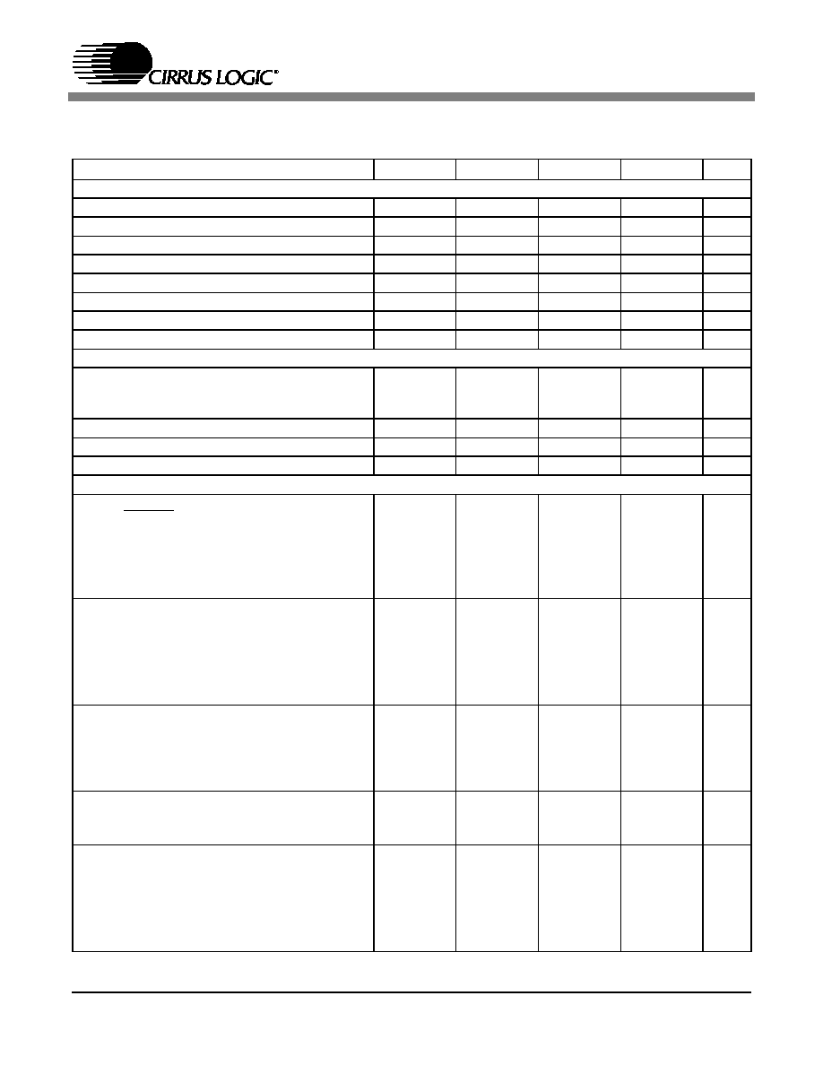
DC CHARACTERISTICS
(Over recommended operating conditions)
Parameter
Symbol
Min
Typ
Max
Unit
External Oscillator
XTAL_I Input Low Voltage
V
IXH
-0.3
-
0.5
V
XTAL_I Input High Voltage
V
IXH
3.5
-
VDD+0.5
V
XTAL_I Input Low Current
I
IXL
-40
-
-
�A
XTAL_I Input High Current
I
IXH
-
-
40
�A
XTAL_I Input Capacitance
C
L
-
35
pF
XTAL_I Input Cycle Time
t
IXC
39.996
-
40.004
ns
XTAL_I Input Low Time
t
IXL
18
-
22
ns
XTAL_I Input High Time
t
XH
18
-
22
ns
Power Supply
Power Supply Current
100BASE-TX (Note 1)
100BASE-FX (Note 1)
10BASE-T (Note 1)
I
DD
-
-
-
135
90
80
145
-
-
mA
Hardware Power-Down
(Note 1)
I
DDHPDN
-
900
-
�A
Software Power-Down
(Note 1)
I
DDSPDN
-
20
-
mA
Low Power Power-Up
(Note 1)
I
DDSLPUP
-
900
-
�A
Digital I/O
Output Low Voltage
CLK25, MII_IRQ, SPD10, SPD100
I
OL
= 4.0mA
LED[4:0]
I
OL
= 10.0mA
V
OL
-
-
-
-
0.4
0.4
V
Output Low Voltage (MII_DRV = 1)
COL, CRS, MDIO, RXD[3:0],
RX_CLK, RX_DV, RX_ER,
TX_CLK
I
OL
= 4.0mA
VDD_MII = 5V; I
OL
= 43.0mA
VDD_MII = 3.3V, I
OL
= 26.0mA
V
OL
-
-
-
-
-
-
0.4
3.05
2.1
V
Output Low Voltage (MII_DRV = 0)
COL, CRS, MDIO, RXD[3:0],
RX_CLK, RX_DV, RX_ER,
TX_CLK
I
OL
= 4.0mA
V
OL
-
-
0.4
V
Output High Voltage
CLK25, SPD10, SPD100
I
OH
= -4.0mA
V
OH
2.4
-
-
V
Output High Voltage (MII_DRV = 1)
COL, CRS, MDIO, RXD[3:0],
RX_CLK, RX_DV, RX_ER,
TX_CLK
I
OH
= -4.0mA
VDD_MII = 5V; I
OH
= -20.0mA
VDD_MII = 3.3V, I
OH
= -20.0mA
V
OH
2.4
1.1
1.1
-
-
-
-
-
-
V