| –≠–ª–µ–∫—Ç—Ä–æ–Ω–Ω—ã–π –∫–æ–º–ø–æ–Ω–µ–Ω—Ç: CDK8920A | –°–∫–∞—á–∞—Ç—å:  PDF PDF  ZIP ZIP |
Copyright
©
Cirrus Logic, Inc. 1997
(All Rights Reserved)
CS8920A
Advanced Product Databook
&U\VWDO /$1
TM
ISA
Plug-and-Play Ethernet
Controller
FEATURES
s
Single-Chip IEEE 802.3 Ethernet Controller with
Direct ISA-Bus Interface
s
Implements Industry-Standard Plug and Play
s
Full Duplex Operation
s
Auto-Negotiation of Full and Half duplex Modes
s
Recognizes Received Magic PacketTM Frames and
Requests the Processor to Power Up
s
Supported by Complete Family of Device Drivers
s
Efficient PacketPageTM Architecture Operates in
I/O and Memory Space, and as DMA Slave
s
On-Chip RAM Buffers Transmit & Receive Frames
s
10BASE-T Port with Internal Analog Filters
s
AUI Port for 10BASE2, 10BASE5 and 10BASE-F
s
Programmable Receive Features:
-- StreamTransfer
TM
for Reduced CPU Overhead
-- Auto-Switch Between DMA and On-Chip Memory
-- Early Interrupts for Frame Pre-Processing
s
Four LED Drivers for Link Status, Full Duplex, and
LAN Activity
s
Small 144-pin TQFP package, and minimal exter-
nal components (transformer, crystal and
optional EEPROM)
DESCRIPTION
The CS8920A is a low-cost Ethernet LAN Control-
ler optimized for Industry Standard Architecture
(ISA) Personal Computers. Its highly-integrated
design eliminates the need for costly external com-
ponents required by other Ethernet controllers.
In addition to high integration, the CS8920A offers
a broad range of performance features and config-
uration options. Its unique PacketPage
architecture automatically adapts to changing net-
work traffic patterns and available system
resources. The result is increased system efficien-
cy and minimized CPU overhead.
The CS8920A is available in a thin 144-pin TQFP
package ideally suited for small form-factor, cost-
sensitive Ethernet applications, such as desktop
and portable motherboards. With the CS8920A,
system engineers can design a complete Plug-
and-Play Ethernet circuit that occupies less than
2.0 square inches (14 sq. cm) of board space.
ORDERING INFORMATION
Contact Cirrus to check on the availability of CS8920A
for use in ISA form-factor adapter-card applications.
CS8920A-CQ0 to 70… C
144-pin TQFP
CDK8920A
Developer's Kit
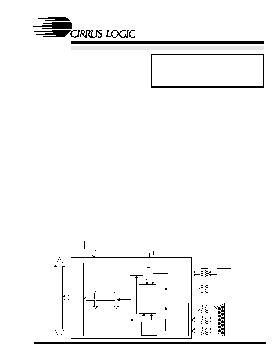
EEPROM
RJ-45
10BASE-T
Attachment
Unit
Interface
(AUI)
20 MHz
XTAL
CS8920 ISA Ethernet Controller
I
S
A
ISA
Bus
Logic
&
Plug
and
Play
EEPROM
Control
RAM
Memory
Manager
802.3
MAC
Engine
and Auto
Negotiation
LED
Control
Clock
Power
Manager
10BASE-T
RX Filters &
Receiver
AUI
Receiver
AUI
Transmitter
AUI
Collision
10BASE-T
TX Filters &
Transmitter
Encoder/
Decoder
&
PLL
SEP `97
DS238PP2
Crystal LAN is a trademark of Cirrus Logic, Inc.
Magic Packet is a trademark of Advanced Micro Devices, Inc.

CONTENTS
1.0
INTRODUCTION
1.1 General Description
. . . .
4
1.2 System Applications
. . . .
5
1.3 Key Features and Benefits . . .
5
1.4 Enhancements Made in CS8920A .
8
2.0
PIN DESCRIPTION
2.1 Pin Diagram
. . . . . .
9
2.2 Pin Description . . . . . . 10
3.0
FUNCTIONAL DESCRIPTION
3.1 Overview
. . . . . . . 14
3.2 ISA Bus Interface . . . . . 15
3.3 Reset and Initialization . . . . 16
3.4 Plug and Play . . . . . . 18
3.5 Configuration with EEPROM . . 19
3.6 Programming the EEPROM
. . 23
3.7 Boot PROM Operation . . . . 24
3.8 Low-Power Modes . . . . . 25
3.9 LED Outputs
. . . . . . 26
3.10 Media Access Control (MAC) . . 27
3.11 Encoder/Decoder (ENDEC)
. . 33
3.12 10BASE-T Transceiver . . . . 34
3.13 Attachment Unit Interface (AUI) . 37
3.14 External Clock Oscillator . . . 38
4.0
PACKETPAGE ARCHITECTURE
4.1 PacketPage Overview . . . . 39
4.2 PacketPage Memory Map . . . 40
4.3 Bus Interface Registers
Product Identification Code . . 42
DMA Start of Frame . . . . 43
DMA Frame Count
. . . . 43
RxDMA Byte Count . . . . 43
EEPROM Command . . . . 44
EEPROM Data
. . . . . 44
Receive Frame Byte Counter . . 44
4.4 Status and Control Registers
. . 45
4.4.1 Status/Control Bit Definitions
46
4.4.2 Status/Control Register Summary 47
4.5 Status/Control Register Details
(0) Interrupt Status Queue
. . 50
(3) Receiver Configuration (RxCFG) 51
(4) Receiver Event (RxEvent)
. 52
(5) Receiver Control (RxCTL)
. 53
(7) Transmit Configuration (TxCFG) 54
(8) Transmit Event (TxEvent)
. 55
(9) Transmit Command (TxCMD)
56
(B) Buffer Configuration (BufCFG)
57
(C) Buffer Event (BufEvent) . . 59
(D) Advance Interrupt Control
and Status (ADVintCTL/ST) . 60
(10) Receive Miss Counter (RxMISS) 61
(12) Trans. Collision Count (TxCOL) 61
(13) Line Control (LineCTL) . . 62
(14) Line Status (LineST) . . . 63
(15) Self Control (SelfCTL) . . 64
(16) Self Status (SelfST) . . . 65
(17) Bus Control (BusCTL) . . 66
(18) Bus Status (BusST) . . . 67
(19) Test Control (TestCTL) . . 68
(1C) AUI Time Domain Reflectometer 69
(1D) Auto Negotiation Control
(AutonegCTL) . . 70
(1E) Auto Negotiation Status
(AutonegST)
. . 71
4.6
Initiate Transmit Register
Transmit Command (TxCMD)
. 72
Transmit Length (TxLength) . . 73
4.7
Address Filter Registers
Logical Address Table (hash table)
74
Individual Address (IEEE address)
74
4.8
Plug n Play Resource Registers
. 75
4.9
Receive and Transmit Frame Locations 80
4.10 8 and 16-bit Transfers . . . . 80
4.11 Memory Mode Operation . . . 81
4.12 I/O Space Operation
. . . . 83
5.0
OPERATION
5.1
Servicing the Interrupt Status Queue
86
5.2
Basic Receive Operation
. . . 88
5.3
Receive Frame Address Filtering . 95
5.4
Rx Missed and Collision Counters . 98
5.5
Receive DMA
. . . . . . 98
5.6
Auto-Switch DMA . . . . . 103
5.7
StreamTransfer . . . . . . 106
5.8
Transmit Operation . . . . . 108
5.9
Full Duplex Considerations . . . 115
5.10 System Wakeup with Wakeup Frames 115
6.0
TEST MODES
6.1
Boundary Scan Test . . . . . 121
7.0
ABSOLUTE MAXIMUM RATINGS
. 125
Recommended Operating Conditions
. 125
8.0
OPERATING CONDITIONS
. . . 125
CS8920A
2
DS238PP2

9.0
DC CHARACTERISTICS
Crystal . . . . . . . . 125
Power Supply . . . . . . 125
Digital Inputs/Outputs . . . . 126
10BASE-T Interface
. . . . 127
AUI Interface
. . . . . . 127
9.1 CAPACITANCE
. . . . . 127
10.0 SWITCHING CHARACTERISTICS
ISA Bus Timing
. . . . . 128
10BASE-T Timing . . . . . 132
AUI Timing . . . . . . . 133
Boot PROM Timing
. . . . 135
EEPROM Timing . . . . . 135
11.0 10BASE-T WIRING DIAGRAM
. . 136
12.0 AUI WIRING DIAGRAM
. . . . 137
13.0 CRYSTAL OSCILLATOR
. . . . 137
14.0 PHYSICAL DIMENSIONS . . . . 138
15.0 GLOSSARY . . . . . . . . 139
CS8920A
DS238PP2
3

1.0
INTRODUCTION
1.1
General Description
The CS8920A is a single-chip, ISA Plug-and-
Pl ay, fu ll-d upl ex, E th erne t s ol uti on,
incorporating all of the analog and digital cir-
c uit ry ne ede d for a compl ete Eth erne t
circuit. Major functional blocks include: indus-
try-standard plug-and-play protocol engine, a
direct ISA-bus interface, an 802.3 MAC engine
with auto-negotiation and wake-up frame recog-
nition capability, integrated buffer memory; a
serial EEPROM interface, and a complete analog
front end with both 10BASE-T and AUI.
Plug and Play
The CS8920A implements Plug and Play in ac-
cordance with the Intel/Microsoft Plug and Play
ISA Specification Version 1.0a, allowing inter-
rupts, DMA channels, IO base address, memory
base address, and optional BootPROM address
to be selected dynamically, by either a system
BIOS, an operating system or an application pro-
gram such as the Configuration Manager. The
CS8920A supports 11 interrupts and 3 DMA
channels.
Direct ISA-Bus Interface
The CS8920A has a direct ISA-bus interface
with full 24 mA drive capability. The CS8920A
operates in either 24-bit memory space, 16-bit
I/O space, or with external DMA controllers
(three 16-bit channels), providing maximum de-
sign flexibility.
Integrated Memory
The CS8920A incorporates a 4-Kbyte page of
on-chip memory, eliminating the cost and board
area associated with external memory chips. Un-
like most other Ethernet controllers, the
CS8920A buffers entire transmit and receive
frames on chip, eliminating the need for com-
plex, inefficient memory management schemes.
The on-chip buffer manager supports full-duplex
operation.
802.3 Ethernet MAC Engine
The CS8920A's Ethernet Media Access Control
(MAC) engine is fully compliant with the IEEE
802.3 Ethernet standard (ISO/IEC 8802-3, 1993),
and supports full-duplex operation. The full-du-
plex mode may be entered by a command from
the host, or via auto-negotiation using link-pulse
signaling.
Magic Packet Frames
The MAC machine recognizes Magic Packet
frames, and can send a wakeup signal to a sys-
tem power management chip via a dedicated
control line or via an interrupt pin.
EEPROM Interface
Th e C S89 20A prov ide s a simpl e seri al
EEPROM interface that allows configuration in-
formation to be stored in EEPROM, and then
loaded automatically at power-up.
Complete Analog Front End
The CS8920A's analog front end incorporates a
Manchester encoder/decoder, clock recovery cir-
cuit, 10BASE-T transceiver, and complete
Attachment Unit Interface (AUI). It provides
manual and automatic selection of either
10BASE-T or AUI, and offers three on-chip
LED drivers for link status, bus status, and Eth-
ernet line activity.
The 10BASE-T transceiver includes drivers, re-
ceivers, and analog filters, allowing direct
connection to low-cost isolation transformers. It
supports 100, 120, and
150
shielded and un-
shielded cables, extended cable lengths.
CS8920A
4
DS238PP1

The AUI port provides a direct interface to
10BASE-2, 10BASE-5 and 10BASE-FL net-
works, and is capable of driving a full 50-meter
AUI cable.
1.2
System Applications
The CS8920A is designed to work well in either
motherboard or adapter applications.
Motherboard LANs
The CS8920A requires the minimum number of
external components needed for an Ethernet
node, allowing a complete Ethernet circuit that
occupies as little as 2.0 square inches of PCB
area (Figure 1.1). In addition, the CS8920A's
power-saving features make it a perfect fit for
power-sensitive portable and desktop PCs. Moth-
erboard design options include:
∑
The EEPROM, used to store node-specific
information, such as the Ethernet Individual
Address, can be eliminated by storing infor-
mation in the system CMOS.
∑
The 20 MHz crystal oscillator may be re-
placed by a 20 MHz clock signal.
Note: while operation of the CS8920A is possi-
ble without the use of an attached EEPROM,
special design considerations are required. Fur-
thermore, some of the CS8920A functions, such
as Plug and Play capabilities and wakeup frame
recognition are not possible without an attached
EEPROM. Please contact Crystal's CS8920A
technical support for more information on the
use of the CS8920A without an attached
EEPROM.
Plug-and-Play Ethernet Adapter Cards
The CS8920A's highly efficient StreamTrans-
fer
TM
and Auto-Switch DMA options, make it
an excellent choice for high-performance, low-
c o s t, ISA ada pte r card s (Fi g. 1 .2 ). T he
CS8920A's wide range of configuration options,
listed below, allow engineers to design Ethernet
solutions that meets their particular system re-
quirements.
∑
A Boot PROM can be added to support disk-
less applications.
∑
The 10BASE-T transmitter and receiver im-
pedance can be adjusted to support 100, 120,
or
150
twisted pair cables.
∑
On-chip LED ports can be used for either
optional LEDs, or as programmable outputs.
1.3
Key Features and Benefits
Very Low Cost
The CS8920A is designed to provide the lowest-
cost Ethernet solutions available for ISA desktop
motherboards, portable motherboards, and
adapter cards. Cost-saving features include:
∑
Integrated RAM eliminates the need for ex-
pensive external memory chips.
RJ-45
10BASE-T
CS8920A
I
S
A
EEPROM 20 MHz
XTAL
(2.0 sq. in.)
Figure 1.1. Complete Ethernet Motherboard Solution
CS8920A
DS238PP1
5

∑
On-chip 10BASE-T filters allow designers to
use simple isolation transformers instead of
more costly filter/transformer packages.
∑
The serial EEPROM port, used for configu-
ration and initialization, eliminates the need
for expensive switches and jumpers.
∑
The CS8920A is designed to be used on a
2-layer circuit board instead of a more ex-
pensive multi-layer board.
∑
The CS8920A-based solution offers the
smallest footprint available, saving valuable
printed circuit board area.
∑
A set of certified software drivers is available
at no charge, eliminating the need for costly
software development.
High Performance
The CS8920A is a full 16-bit Ethernet controller
designed to provide optimal system performance
by minimizing time on the ISA bus and CPU
overhead per frame. It offers equal or superior
performance for less money when compared to
other Ethernet controllers. The CS8920A's Pack-
etPage architecture allows software to select
whichever access method is best suited to each
particular CPU/ISA-bus configuration. When
compared to older I/O-space designs, PacketPage
is faster, simpler and more efficient.
To boost performance further, the CS8920A in-
c l ud e s e ve ra l k ey f ea t ur es th a t inc rease
throughput and lower CPU overhead, including:
∑
StreamTransfer cuts up to 87% of interrupts
to the host CPU during large block transfers.
∑
Auto-Switch DMA allows the CS8920A to
maximize throughput while minimizing
missed frames.
∑
Early interrupts allow the host to preprocess
incoming frames.
∑
On-chip buffering of full frames cuts the
amount of host bandwidth needed to manage
Ethernet traffic.
Low Power and Low Noise
For low power needs, the CS8920A offers three
power-down options: Hardware Standby, Hard-
ware Suspend, and Software Suspend. In
Standby mode, the chip is powered down with
the exception of the 10BASE-T receiver, which
is enabled to listen for link activity. In either
Hardware or Software Suspend mode, the re-
CS8920A
EEPROM
Boot PROM
'245
20 MHz
XTAL
RJ-45
LED
Attachment
Unit
Interface
(AUI)
Figure 1.2. Full-Featured ISA Adapter Solution
CS8920A
6
DS238PP1

EECS
EEDATAOUT
EESK
SA[0:16]
MEMW
MEMR
IOW
IOR
REFRESH
SBHE
SD[0:15]
RXD-
RXD+
TXD-
TXD+
DO-
DO+
CI-
CI+
DI-
DI+
LANLED
LINKLED/HC0
CSOUT
EEDATAIN
AEN
RESET
DRQ5
DACK5
DRQ6
DACK6
DRQ7
DACK7
MEMCS16
IOCHRDY
1:
68 pF
1
3
6
8
24.3
, 1%
24.3
, 1%
130
129
126
125
100
, 1%
RJ45
16
14
11
9
10
6
3
2
1
1:1
1
4
5
8
122
120
119
117
16
13
12
9
10
10
9
2
5
121
118
2
7
15
3
12
1:1
1:1
0.1
µ
F
.1
µ
F
680
680
CE
OE
OE
DIR
20
22
19
1
74LS245
XTAL1 XTAL2
SLEEP
TEST
RES
CS
DO
DI
CLK
1
3
2
4
141
6
142
7
93C56
28
90
89
29
7
IRQ3
IRQ4
IRQ5
IRQ6
16
17
LA[17:23]
BALE
135
136
131
4.99 k
, 1%
12 V
6
20 MHz
0.1
µ
F
39.2
, 1%
5 V
4.7 k
CS8920A
IOCS16
83
91
114
52
44
92
43
75
77
78
76
16
14
15
17
9
10
139
140
8
39.2
, 1%
39.2
, 1%
39.2
, 1%
EEPROM
27C256
2
ISA
BUS
10 BASE T
Isolation
Transformer
1:1
15 pin D
AUI Isolation
Transformer
BSTATUS/HCI
Boot-PROM
PD[0:7]
SA[0:14]
SD[0:7]
15
8
LOCALLED
IRQ7
IRQ9
IRQ10
IRQ11
IRQ12
IRQ14
IRQ15
57
34
33
31
32
106
79
30
5
113
115
.1
µ
F
2
EWAKE
680
3
116
Figure 1.3. Typical Connection Diagram
CS8920A
DS238PP1
7

ceiver is disabled and power consumption drops
to the micro-Amp range.
In addition, the CS8920A has been designed for
very low noise emission, thus shortening the
time required for EMI testing and qualification.
Complete Support
The CS8920A comes with a suite of software
drivers for immediate use with most industry
standard network operating systems. In addition,
complete evaluation kits and manufacturing
packages are available, significantly reducing the
cost and time required to produce new Ethernet
products.
1.4
Enhancements Made in CS8920A
The functional enhancements made to the
CS8920A include the following:
The FDX_LED pin of the CS8920 has been red-
fined as the local-LAN-activity LED on the
CS8920A. The LOCALLED will light when
one of two events occurs:
∑
the CS8920A transmits onto the network, or
∑
the CS8920A receives a frame from the net-
work and that frame is addressed to this
station (i.e., the frame's address passes the
CS8920A's address filter).
The Plug and Play standard provides for an Aux-
illary Key which is normally used for testing
purposes or to program the EEPROM. The
CS8920A will respond to the Auxillary Key at
any time. The CS8920 responded to the Auxil-
lary Key only if Plug and Play was enabled, or if
the CS8920 had detected that the EEPROM con-
tained a bad CRC value. This meant that the
CS8920 would ignore the Auxillary Key in non-
Plug and Play mode as long as the CRC was
valid.
To support software compatibility with existing
device drivers, the CS8920A's Product Identifi-
cation Code register has the same Product ID
Number as the CS8920. The CS8920A's revi-
sion number has been incremented.
The CS8920A has added the EWAKE pin to the
boundary scan.
CS8920A
8
DS238PP1

2.0
PIN DESCRIPTION
2.1
Pin Diagram
14
4
14
3
14
2
14
0
13
9
13
8
13
7
13
6
13
5
14
1
13
4
13
3
13
2
13
1
13
0
12
9
128
127
12
6
12
5
12
4
12
3
12
2
121
120
LOCALLED
EEDO
EEDI
CSOUT
DRQ7
DACK7
ASUB1
DVSS1
DVDD1
DSUB1
DRQ6
DACK6
DRQ5
DACK5
SD15
SD14
SD13
SD12
DVDD2
DVSS2
SD11
SD10
IO
C
S
1
6
MC
S
1
6
LA
1
7
LA
1
8
LA
1
9
LA
2
0
LA
2
1
LA
2
2
LA
2
3
SB
HE
DS
U
B
2
D
V
DD3
D
VSS3
BA
L
E
SA
0
SA
1
SA2
SA
3
EE
S
K
EE
C
S
L
ANL
ED
L
I
N
K
L
E
D/
HC
0
XT
A
L
2
XT
A
L
1
AS
U
B
2
AV
D
D
1
A
VSS
1
RE
S
RX
D
-
RX
D
+
AV
D
D
2
AV
S
S
2
TX
D
-
TX
D
+
A
VSS
3
AV
D
D
3
DO-
DO
+
CI
-
CS8920A
144-Pin
TQFP
(Q)
SD9
SD8
MEMW
MEMR
IRQ14
IRQ15
IRQ12
IRQ11
IRQ10
37
38
39
41
42
43
44
45
46
40
47
48
49
50
51
52
53
54
55
56
57
58
59
60
61
SA4
SA
5
SA6
SA
7
SA
8
62
63
64
65
66
67
68
69
70
71
72
108
107
106
104
103
102
101
100
99
105
98
97
96
95
94
93
92
91
90
89
88
87
86
85
84
IRQ2/IRQ9
SD6
SD5
SD4
DVDD5
DVSS5
SD3
SD7
SD2
SD1
SD0
DSUB3
DVDD4
DVSS4
IOCHRDY
AEN
IOW
IOR
SA16
SA15
SA14
SA13
SA12
83
82
81
80
79
78
77
76
75
74
73
REFRESH
SA11
SA10
SA9
IRQ7
IRQ6
IRQ5
IRQ4
IRQ3
119
118
117
11
6
11
5
11
4
11
3
11
2
11
1
11
0
10
9
CI
+
DI
-
DI
+
SL
EE
P
TE
ST
RES
E
T
BS
TAT
U
S
/
H
C
1
1
2
3
5
6
7
8
9
10
4
11
12
13
14
15
16
17
18
19
20
21
22
23
24
25
26
27
28
29
30
31
32
33
34
35
36
AS
U
B
3
AS
UB4
EWAKE
CS8920A
DS238PP2
9

2.2
Pin Description
ISA Bus Interface
Symbol
Pin Number
Type
Description
SA0-SA8
SA9-SA11
SA12-SA16
58-66
80-82
84-88
I
System Address Bus: Address decoding for the ISA addresses including
Boot PROM and memory addresses. SA0-SA15 are used for I/O read/write
operations. SA0-SA16 are used in for Memory read and write operations.
LA17-LA23
45-51
I
Latchable Address Bus: Address decoding for the buffered version of the
upper ISA address bits. Used for early address decode. Latched on the
trailing edge of the BALE signal.
BALE
57
I
Buffered Address Latch Enable: Rising edge signals the CS8920A to
decode the LA17:LA23. The trailing edge of BALE is used to latch the
address and hold it for the duration of the current bus cycle.
SD0-SD3
SD4-SD7
SD8-SD11
SD12-SD15
96-99
102-105
27-24
21-18
B24
System Data Bus: Bi-directional 16-bit System Data Bus used to transfer
data between the CS8920A and the host.
RESET
114
I
Reset: Active-high asynchronous input used to reset the CS8920A. Must
be stable for at least 400 ns before the CS8920A recognizes the signal as
a valid reset.
AEN
91
I
Address Enable: When TEST is high, the active-high AEN input indicates
to the CS8920A that the system DMA controller has control of the ISA bus.
When AEN is high, the CS8920A will not respond to an IO or Memory
space access.
MEMR
29
I
Memory Read: Active-low input indicates that the host is executing a
Memory Read operation.
MEMW
28
I
Memory Write: Active-low input indicates that the host is executing a
Memory Write operation.
MCS16
44
OD24 Memory Chip Select 16: Open-drain, active-low output generated by the
CS8920A when it recognizes an address on the ISA bus that corresponds
to its assigned Memory space (CS8920A must be in Memory Mode with
the MemoryE bit (Register 17, BusCTL, Bit A) set for MCS16 to go active).
Tri-stated when not active.
REFRESH
83
I
Refresh: Active-low input indicates to the CS8920A that a DRAM refresh
cycle is in progress. When REFRESH is low, MEMR, MEMW, IOR, IOW,
DMACK0, DMACK1, and DMACK2 are ignored.
IOR
89
I
I/O Read: When IOR is low and a valid address is detected, the CS8920A
outputs the contents of the selected 16-bit I/O register onto the System
Data Bus. IOR is ignored if REFRESH is low.
IOW
90
I
I/O Write: When IOW is low and a valid address is detected, the
CS8920A writes the data on the System Data Bus into the selected 16-bit
I/O register. IOW is ignored if REFRESH is low.
Pin Types:
dI
=
Differential Input Pair
I
=
Input
G
=
Ground
dO
=
Differential Output Pair
O
=
Output
ts
=
Tri-State
B
=
Bi-Directional with Tri-State Output P
=
Power
w
=
Internal Weak Pullup
OD
=
Open Drain Output
Digital outputs are followed by drive in mA (Example: OD24 = Open Drain Output with 24 mA drive).
CS8920A
10
DS238PP2

ISA Bus Interface (continued)
Symbol
Pin Number
Type
Description
IOCS16
43
OD24 I/O Chip Select 16-bit: Open-drain, active-low output generated by the
CS8920A when it recognizes an address on the ISA bus that
corresponds to its assigned I/O space. Tri-stated when not active.
IOCHRDY
92
OD24 I/O Channel Ready: When driven low, this open-drain, active-high
output extends I/O Read and Memory Read cycles to the CS8920A. This
output is functional when the IOCHRDYE bit in the Bus Control register
(Register 17) is clear. This pin is always tri-stated when the IOCHRDYE
bit is set.
SBHE
52
I
System Bus High Enable: Active-low input indicates a data transfer on
the high byte of the System Data Bus (SD8-SD15). After a hardware or
software reset, provide a HIGH to LOW and then a LOW to HIGH
transition on SBHE signal before any IO or memory access isdone to the
CS8920A. *
IRQ2/IRQ9
IRQ3-IRQ7
IRQ10-IRQ12
IRQ14-IRQ15
106
75-79
34-32
30-31
O24ts Interrupt Request: Active-high output indicates the presence of an
interrupt event. The pin goes low after the host reads a non-zero value
from the Interrupt Status Queue (ISQ).
DRQ5
DRQ6
DRQ7
16
14
9
O24ts DMA Request: Active-high, tri-stateable output used by the CS8920A to
request a DMA transfer. Only one DMA Request output is used (one is
selected during configuration). All non-selected DMA Request outputs
are placed in a high-impedance state.
DACK5
DACK6
DACK7
17
15
10
I
DMA Acknowledge: Active-low input indicates acknowledgment by the
host of the corresponding DMA Request output.
EEPROM and Boot PROM Interface
Symbol
Pin Number
Type
Description
EESK
142
O4
EEPROM Serial Clock: Serial clock used to clock data into or out of the
EEPROM.
EECS
141
O4
EEPROM Chip Select: Active-high output used to select the EEPROM.
EEDI
7
Iw
EEPROM Data In: Serial input used to receive data from the EEPROM.
Connects to the DO pin on the EEPROM. EEDI is also used to sense the
presence of the EEPROM.
EEDO
6
O4
EEPROM Data Out: Serial output used to send data to the EEPROM.
Connects to the DI pin on the EEPROM. When TEST is low, this pin
becomes the output for the Boundary Scan Test.
CSOUT
8
O4
Chip Select for External Boot PROM: Active-low output used to select
an external Boot PROM when the CS8920A decodes a valid Boot PROM
memory address.
Pin Types:
dI
=
Differential Input Pair
I
=
Input
G
=
Ground
dO
=
Differential Output Pair
O
=
Output
ts
=
Tri-State
B
=
Bi-Directional with Tri-State Output P
=
Power
w
=
Internal Weak Pullup
OD
=
Open Drain Output
Digital outputs are followed by drive in mA (Example: OD24 = Open Drain Output with 24 mA drive).
* For operation of the CS8920A in 16 bit mode, a transition on the SBHE line is required after a hardware or
software reset.
CS8920A
DS238PP2
11

Attachment Unit Interface (AUI)
Symbol
Pin Number
Type
Description
DO+
DO-
121
122
dO
AUI Data Out: Differential output pair drives 10 Mb/s
Manchester-encoded data to the AUI transmit pair.
DI+
DI-
117
118
dI
AUI Data In: Differential input pair receives 10 Mb/s Manchester-encoded
data from the AUI receive pair.
CI+
CI-
119
120
dI
AUI Collision In: Differential input pair connects to the AUI collision pair.
A collision is indicated by the presence of a 10 MHz +/-15% signal with
duty cycle no worse than 60/40.
10BASE-T Interface
Symbol
Pin Number
Type
Description
TXD+
TXD-
125
126
dO
10BASE-T Transmit: Differential output pair drives 10 Mb/s
Manchester-encoded data to the 10BASE-T transmit pair.
RXD+
RXD-
129
130
dI
10BASE-T Receive: Differential input pair receives 10 Mb/s
Manchester-encoded data from the 10BASE-T receive pair.
Pin Types:
dI
=
Differential Input Pair
I
=
Input
G
=
Ground
dO
=
Differential Output Pair
O
=
Output
ts
=
Tri-State
B
=
Bi-Directional with Tri-State Output P
=
Power
w
=
Internal Weak Pullup
OD
=
Open Drain Output
Digital outputs are followed by drive in mA (Example: OD24 = Open Drain Output with 24 mA drive).
CS8920A
12
DS238PP2

General Pins
Symbol
Pin Number
Type
Description
XTAL1
XTAL2
135
136
I/O
Crystal: A 20 MHz crystal should be connected across these pins. If a
crystal is not used, a 20 MHz signal should be connected to XTAL1 and
XTAL2 should be left open. (See section 9.0 and 13.0.)
SLEEP
116
IW
Hardware Sleep: Active-low input used to enable the two hardware sleep
modes: Hardware Suspend and Hardware Standby. (See section 3.8.)
EWAKE
3
O4w
Wakeup Signal: The CS8920A asserts EWAKE high when a wakeup
frame is detected on the Ethernet receiver.
LINKLED
or
HC0
139
OD10 Link Good LED or Host Controlled Output 0: When the HCE0 bit of the
Self Control register (Register 15) is clear, this active-low output is low
when the CS8920A detects the presence of valid link pulses. When the
HCE0 bit is set, the host may drive this pin low by setting the HCBO in the
Self Control register.
BSTATUS
or
HC1
113
OD10 Bus Status or Host Controlled Output 1: When the HCE1 bit of the Self
Control register (Register 15) is clear, this active-low output is low when
receive activity causes an ISA bus access. When the HCE1 bit is set, the
host may drive this pin low by setting the HCB1 in the Self Control register.
LANLED
140
OD10 LAN Activity LED: During normal operation, this active-low output goes
low for 6 ms whenever there is a receive packet, a transmit packet, or a
collision. During Hardware Standby mode, this output is driven low when
the receiver detects network activity.
LOCALLED
5
OD10 Local Activity LED: During normal operation, this active-low output goes
low for 6 ms whenever there is either a receive packet addressed to this
node, or a transmit packet.
TEST
115
IW
Test Enable: Active-low input used to put the CS8920A in Boundary Scan
Test mode. For normal operation, this pin should be high or left open.
RES
131
I
Reference Resistor: This input should be connected to a 4.99 K
+/-1%
resistor needed for biasing of internal analog circuits.
DVDD1 -
DVDD5
12, 22,
55, 94, 101
P
Digital Power: Provides 5 V +/- 5% power to the digital circuits of the
CS8920A.
DVSS1 -
DVSS5
11, 23, 56,
93, 100
G
Digital Ground: Provides ground reference (0V) to the digital circuits of the
CS8920A.
DSUB1 -
DSUB3
13, 54,
95
Provide additional ground references (0V) to digital circuits of the CS8920A.
AVDD1 -
AVDD3
133, 128,
123
P
Analog Power: Provides 5 V +/- 5% power to the analog circuits of the
CS8920A.
AVSS1 -
AVSS7
4, 124, 127,
132, 134,
137, 138
G
Analog Ground: Provide ground reference (0V) to the analog circuits of the
CS8920A.
AVSS1 -
AVSS4
4, 134,
137, 138
Provided additional ground references (0V) to analog circuits of the
CS8920A.
Pin Types:
dI
=
Differential Input Pair
I
=
Input
G
=
Ground
dO
=
Differential Output Pair
O
=
Output
ts
=
Tri-State
B
=
Bi-Directional with Tri-State Output P
=
Power
w
=
Internal Weak Pullup
OD
=
Open Drain Output
Digital outputs are followed by drive in mA (Example: OD24 = Open Drain Output with 24 mA drive).
CS8920A
DS238PP2
13

3.0
FUNCTIONAL DESCRIPTION
3.1
Overview
During normal operation, the CS8920A performs
two basic functions: Ethernet packet transmis-
sion and reception. Before transmission or
reception is possible, the CS8920A must be con-
figured.
Configuration
The CS8920A must be configured for packet
transmission and reception at power-up or reset.
Various parameters must be written into its inter-
nal Configuration and Control registers such as
Memory Base Address; Ethernet Physical Ad-
dress; what frame types to receive; and which
media interface to use. Configuration data can
either be written to the CS8920A by the host
(across the ISA bus), or loaded automatically
from an external EEPROM. Operation can begin
after configuration is complete.
Sections 3.1 and 3.3 describe the configuration
process in detail. Section 4.4 provides a detailed
description of the bits in the Configuration and
Control Registers.
Packet Transmission
Packet transmission occurs in two phases. In the
first phase, the host moves the Ethernet frame
into the CS8920A's buffer memory. The first
phase begins with the host issuing a Transmit
Command. This informs the CS8920A that a
frame is to be transmitted and tells the chip
when (i.e. after 5, 381, or 1021 bytes have been
transferred or after the full frame has been trans-
ferred to the CS8920A) and how the frame
should be sent (i.e. with or without CRC, with or
without pad bits, etc.). The host follows the
Transmit Command with the Transmit Length,
indicating how much buffer space is required.
When buffer space is available, the host writes
the Ethernet frame into the CS8920A's internal
memory, either as a Memory or I/O space opera-
tion.
In the second phase of packet transmission, the
CS8920A converts the frame into an Ethernet
packet, then transmits it onto the network. The
second phase begins with the CS8920A transmit-
ting the preamble and Start-of-Frame delimiter
as soon as the proper number of bytes have been
transferred into its transmit buffer (5, 381, 1021
bytes or full frame, depending on configuration).
The preamble and Start-of-Frame are followed
by the Destination Address, Source Address,
Length field and LLC data (all supplied by the
host). If the frame is less than 64 bytes, includ-
i ng CRC , the CS8920A adds pad bits if
configured to do so. Finally, the CS8920A ap-
pends the proper 32-bit CRC value.
Section 5.8 provides a detailed description of
packet transmission.
Packet Reception
Like packet transmission, packet reception oc-
curs in two phases. In the first phase, the
CS8920A receives an Ethernet packet and stores
it in on-chip memory. The first phase begins
with the receive frame passing through the ana-
log front end and Manchester decoder where
Manchester data is converted to NRZ data. Next,
the preamble and Start-of-Frame delimiter are
stripped off and the receive frame is sent through
the address filter. If the frame's Destination Ad-
dress matches the criteria programmed into the
address filter, the packet is stored in the
CS8920A's internal memory. The CS8920A then
checks the CRC, and depending on the configu-
ration, informs the processor that a frame has
been received.
In the second phase, the host transfers the re-
ceive frame across the ISA bus and into host
memory. Receive frames can be transferred as
Memory space operations, I/O space operations,
or as DMA operations using host DMA. In addi-
CS8920A
14
DS238PP2

tion, the CS8920A provides the capability to
switch between Memory or I/O operation and
DMA operation by using Auto-Switch DMA and
StreamTransfer.
Sections 5.2 through 5.7 provide a detailed de-
scription of packet reception.
Reset/Boot/Sleep
Nine resets can be activated on the CS8920A.
Three are activated by the V
CC
power supply
line; one is activated when the EEPROM fails
checksum; one is activated on a Plug and Play
instruction; one is activated when RESET is set;
and three are activated with sleep modes.
A sleep mode disables the CS8920A (completely
or partially) to reduce power consumption. "Sus-
pend" describes the CS8920A in the completely
d isa b le d mo de . "S tan dby " descri bes th e
CS8920A in the partially disabled mode when
most of its circuits except the receiver are dis-
abled. The CS8920A can be "Awakened" when
the receiver detects and receives line activity.
After reset, packet transmission and reception are
disabled. Either an external EEPROM must be
used to start the CS8920A, or the host must di-
rectly set up registers using Plug and Play
protocols.
Contact Crystal's CS8920A technical support for
more information regarding the use of the
CS8920A without an external EEPROM.
3.2
ISA Bus Interface
The CS8920A provides a direct interface to ISA
buses running at clock rates from 8 to 11 MHz.
Its on-chip bus drivers are capable of delivering
24 mA of drive current, allowing the CS8920A
to drive the ISA bus directly, without added ex-
ternal "glue logic".
The CS8920A is optimized for 16-bit data trans-
fers, operating in either Memory space, I/O
space, or as a DMA slave.
Note that ISA-bus operation below 8 MHz
should use the CS8920A's Receive DMA mode
to minimize missed frames. See Section 5.5 for a
description of Receive DMA operation.
Memory Mode Operation
When configured for Memory Mode operation,
the CS8920A's internal RAM is mapped into a
contiguous 4-Kbyte block of host memory, pro-
viding the host with direct access to the
CS8920A's internal registers and frame buffers.
The host initiates Read operations by driving the
MEMR pin low and Write operations by driving
the MEMW pin low.
For additional information about Memory Mode,
see Section 4.11.
I/O Mode Operation
When configured for I/O Mode operation, the
CS8920A is accessed through eight, 16-bit I/O
ports that are mapped into sixteen contiguous
I/O locations in the host system's I/O space. I/O
Mode is the default configuration for the
CS8920A and is always enabled.
For an I/O Read or Write operation, the AEN pin
must be low, and the 16-bit I/O address on the
ISA System Address bus (SA0 - SA15) must
match the address space of the CS8920A. For a
Read, IOR must be low, and for a Write, IOW
must be low.
For additional information about I/O Mode, see
Section 4.12.
Interrupt Request Signals
The CS8920A has eleven interrupt request out-
put pins that can be connected directly to any
CS8920A
DS238PP2
15
eleven of the ISA bus Interrupt Request signals.
Only one interrupt output is used at a time. The
interrupt output is selected during initialization
by writing the interrupt number (0 to 10) into
PacketPage Memory base + 0370h; or, the inter-
rupt output can be accessed through the Plug and
Play resource register 0070h. Unused interrupt
request pins are placed in a high-impedance
state. The selected interrupt request pin goes
high when an enabled interrupt is triggered. The
pin goes low after the Interrupt Status Queue
(ISQ) is read as all 0's (see Section 5.1 for a
description of the ISQ).
Table 3.1 presents one possible way of connect-
ing the interrupt request pins to the ISA bus that
utilizes commonly available interrupts and facili-
tates board layout.
*When in PnP mode, the interrupt request output
is accessed through the resource register 0370h.
DMA Signals
The CS8920A interfaces directly to the host
DMA controller to provide DMA transfers of re-
ceive frames from CS8920A memory to host
memory. The CS8920A has three pairs of DMA
pins that can be connected directly to the three
16-bit DMA channels of the ISA bus. Only one
DMA channel is used at a time. It is selected
during initialization by writing the number of the
desired channel (0, 1 or 2) into PacketPage
Memory base + 0374h. Unused DMA pins are
placed in a high-impedance state. The selected
DMA request pin goes high when the CS8920A
has received frames to transfer to the host mem-
ory via DMA. If the DMABurst bit (register 17,
BusCTL, Bit B) is set, the pin goes low after the
DMA operation is complete. If the DMABurst
bit is clear, the pin goes low 32
µ
s after the start
of a DMA transfer.
T he DMA pin pairs are arranged on the
CS8920A to facilitate board layout. Crystal rec-
ommends the configuration in Table 3.2 when
connecting these pins to the ISA bus.
For a description of DMA mode, see Section
5.5.
3.3
Reset and Initialization
3.3.1
Reset
Nine different conditions cause the CS8920A to
reset its internal registers and circuits.
External Reset, or ISA Reset: There is a chip-
wide reset whenever the RESET pin is high for
at least 40 ns. During a chip-wide reset, all cir-
cuitry and registers in the CS8920A are reset.
Power-Up Reset: When power is applied, the
CS8920A maintains reset until the voltage at the
supply pins reaches approximately 2.5 V. The
CS8920A comes out of reset once Vcc is greater
CS8920A Interrupt
Request Pin
ISA Bus
Interrupt
PacketPage
base + 0370h*
IRQ3(Pin 75)
IRQ3
0003h
IRQ4 (Pin 76)
IRQ4
0004h
IRQ5 (Pin 77)
IRQ5
0005h
IRQ6(Pin 78)
IRQ6
0006h
IRQ7(Pin 79)
IRQ7
0007h
IRQ9(Pin 106)
IRQ9
0009h
IRQ10(Pin 34)
IRQ10
000Ah
IRQ11(Pin 33)
IRQ11
000Bh
IRQ12(Pin 32)
IRQ12
000Ch
IRQ14(Pin 30)
IRQ14
000Eh
IRQ15 (Pin 31)
IRQ15
000Fh
Table 3.1. Interrupt Assignments
CS8920A DMA
Signal (Pin #)
ISA DMA
Signal
PacketPage
base + 0374h
DRQ5 (16)
DRQ5
0000h
DACK5 (17)
DACK5
DRQ6 (14)
DRQ6
0001h
DACK6 (15)
DACK6
DRQ7 (9)
DRQ7
0002h
DACK7 (10)
DACK7
Table 3.2. DMA Assignments
CS8920A
16
DS238PP2

than approximately 2.5 V and the crystal oscilla-
tor has stabilized.
Power-Down Reset: If the supply voltage drops
below approximately 2.5 V, there is a chip-wide
reset. The CS8920A comes out of reset once the
power supply returns to a level greater than ap-
proximately 2.5 V and the crystal oscillator has
stabilized.
EEreset: There is a chip-wide reset if the
CS8920A detects an EEPROM checksum error.
(see Section 3.1).
Software Initiated Reset: There is a chip-wide
reset whenever the RESET bit (Register 15,
SelfCTL, Bit 6) is set. The Plug and Play card
select number, Plug and Play Rd Data port,
PnP_disable bit, IO base address register, mem-
ory base address register, interrupt register, and
DMA register are preserved. The digital logic is
reset, but the analog circuits are not.
Hardware (HW) Standby or Suspend: Th e
CS8920A goes though a chip-wide reset when-
ever it enters or exits either HW Standby mode
or HW Suspend mode (see Section 3.8 for more
information about HW Standby and Suspend).
Software (SW) Suspend: Wh en ever th e
CS8920A enters SW Suspend mode, all registers
and circuits are reset except for the ISA I/O Base
Address register (located at PacketPage base +
0360h) and the SelfCTL register (Register 15).
Upon exit, there is a chip-wide reset (see Section
3.8 for more information about SW Suspend).
PnP Initiated Reset: Writing a one (setting
bit[0]) to the Plug and Play Config Control reg-
ister (address 0x02) causes all digital registers to
be reset, including the CS8920A's Card select
Number and Plug and Play Read Data Port ad-
dress. At the end of the reset, the CS8920A will
attempt to read configuration information from
EEPROM. The analog circuits are not reset.
Magic Packet Frame Generated Reset: In power
down mode, with WakeupEn=1, the CS8920A
won't reset completely unless the reset signal it
detects is followed by 6 MEMR cycles. The
Magic Packet frame generated reset ensures the
CS8920A resets only when it receives a true
power up reset signal.
3.3.2
Allowing Time for Reset Operation
After a reset, the CS8920A goes through a self
configuration. This includes calibrating on-chip
analog circuitry, and reading EEPROM for valid-
ity and configuration. Time required for the reset
calibration is typically 10 ms. Software drivers
should not access registers internal to the
CS8920A during this time. When calibration is
done, bit INITD in the Self Status Register (reg-
ister 16) is set indicating that initialization is
complete, and the SIBUSY bit in the same regis-
ter is cleared indicating the EEPROM is no
longer being read or programmed.
3.3.3
Bus Reset Considerations
The CS8920A reads 3000h from IObase+0Ah
after the reset, until the software writes a non-
zero value at IObase+0Ah. The 3000h address
can be used as part of the CS8920A signature
when the system scans for the CS8920A. See
Section 4.12, I/O Space Operation.
After a reset, the ISA bus outputs IRQx and
DRQx are tri-stated, thus avoiding any interrupt
or DMA channel conflicts on the ISA bus at
power-up time.
Initialization
After each reset (except EEPROM Reset), the
CS8920A checks the sense of the EEDI pin to
see if an external EEPROM is present. If EEDI
i s h i gh , a n E E PROM is p resent an d t he
CS8920A automatically loads the configuration
data stored in the EEPROM into its internal reg-
isters (see next section). If EEDI is low, an
CS8920A
DS238PP2
17
EEPROM is not present and the CS8920A
comes out of reset with the default configuration
shown in Table 3.3.
A low-cost serial EEPROM can be used to store
configuration information that is automatically
loaded into the CS8920A after each reset (except
EEPROM reset). The use of an EEPROM is op-
tional and is not required for all applications
(e.g. motherboard designs). However, while op-
eration of the CS8920A is possible without the
use of an attached EEPROM, special design con-
siderations are required. Furthermore, some of
the CS8920A functions, such as Plug and Play
capabilities and wakeup frame recognition are
not possible without an attached EEPROM. Con-
tact Crystal's CS8920A technical support for
more information on the use of the CS8920A
without an attached EEPROM.
The CS8920A operates with any of six standard
EEPROM's shown in Table 3.4. To work in a
PNP system, the CS8920A requires at least a
128 word EPROM.
3.4
Plug & Play
Plug and Play is a standard mechanism, devel-
oped by Intel and Microsoft, that provides an
automatic configuration capability for ISA cards.
System resources such as interrupts, memory ad-
dresses, and IO ports are assigned to Plug and
Play compatible devices by the Plug and Play
configuration mechanism.
The CS8920A fully supports Plug and Play and
allows the complete configuration of the ISA in-
terface by the Plug and Play compatible
operating system software or BIOS. Refer to the
Plug and Play ISA Specification for detailed in-
formation about the innerworkings of Plug and
Play.
Plug and Play Configuration Process
The Plug and Play configuration process deter-
mines the resource requirements of the Plug and
Play devices in a system and assigns non-con-
f li c ti n g re s ou rc e s t o th e s e ca rd s . T he
configuration process goes through several
phases:
PacketPage
Address
Register
Contents
Register
Description
0360h
0000h
I/O Base Address*
0370h
XXXX XXXX
0000 0000
Interrupt Number
0374h
XXXX XXXX
XXXX XX11
DMA Channel
0026h
0000h
DMA Start-of-Frame Offset
0028h
X000h
DMA Frame Count
002Ah
0000h
DMA Byte Count
0348h
XXX0 0000h
Memory Base Address
0340h
XXX0 0000h
Boot PROM Base
Address
0343h
XXX0 0000h
Boot PROM Address Mask
0102h
0003h
Register 3 - RxCFG
0104h
0005h
Register 5 - RxCTL
0106h
0007h
Register 7 - TxCFG
0108h
0009h
Register 9 - TxCMD
010Ah
000Bh
Register B - BufCFG
010Ch
000Dh
Register D - Advint CTL/ST
010Eh
Undefined
Reserved
0110h
Undefined
Reserved
0112h
0013h
Register 13 - LineCTL
0114h
0015h
Register 15 - SelfCTL
0116h
0017h
Register 17 - BusCTL
0118h
0019h
Register 19 - TestCTL
011Ch
001Dh
Register ID - AutoNeg CTL
* I/O base address is unaffected by SW Suspend mode.
Table 3.3. Default Configuration
EEPROM Type
Size (16-bit words)
'C46 (non-sequential)
64
'CS46 (sequential)
64
'C56 (non-sequential)
128
'CS56 (sequential)
128
'C66 (non-sequential)
256
'CS66 (sequential)
256
Table 3.4. Supported EEPROM Types
CS8920A
18
DS238PP2

∑
A reset signal on the system bus places all
Plug and Play cards into a mode in which
they are all waiting for configuration to be-
gin.
∑
A special key is written to all all of the PNP
cards to initialize them for selection.
∑
A special series of reads is performed that
allows a single card to be selected. The se-
lected card is given a system identifier, called
the card select number (CSN). The configu-
ration software then determines the resource
requirements of the card. Finally, the selected
card is placed into a sleep mode. The remain-
ing cards are individually selected and
assigned a CSN and their resource needs de-
termined.
∑
The configuration software then selects an
individual card using the CSN, assigns non-
conflicting resources to the card, and then
enables the card for normal operation. This is
repeated for each of the Plug and Play cards
until all of the cards have been configured
and enabled.
Plug and Play Auxiliary Key
The CS8920A will respond to a special auxiliary
key at any time. The auxiliary initiation key is
normally used for testing/debug purposes. Two
bytes of 00 should proceed the initiation or aux-
iliary key. This auxiliary initiation key is listed
below in hexadecimal:
6A, B5, DA, 6D, B6, 5B, 2D, 16
0B, 05, 02, 01, 80, C0, 60, 30
18, 0C, 06, 83, 41, 20, 90, 48
24, 12, 89, C4, E2, F1, F8, FC
Plug and Play Device IDs
The Plug and Play device ID is a unique identi-
fier that is used by the operating system to
associate the Plug and Play card with its device
driver. Microsoft administers the assignment of
these device IDs. Contact Microsoft to receive a
unique device ID.
3.5
Configuration with EEPROM
EEPROM Interface
The interface to the EEPROM consists of the
four signals shown in Table 3.5
EEPROM Memory Organization
EEPROM is used to store initial configuration
information for the CS8920A. The EEPROM is
organized in one or more blocks of 16-bit words.
The first block in EEPROM, referred to as the
Configuration Block, is used to configure the
CS8920A after reset. An example of a typical
Configuration Block is shown in Table 3.6 . Ad-
ditional user data may also be stored in the
EEPROM if space is available. The additional
data are stored as 16-bit words and can occupy
any EEPROM address space beginning immedi-
ately after the end of the Reset Configuration
B l oc k up to add ress 7 Fh, dep end ing on
EEPROM size. This additional data can only be
accessed through software control (refer to Sec-
tion 3.6 for more information on accessing the
EEPROM). Address space 80h to AFh is re-
served
CS8920A Pin
(Pin #)
CS8920A Function
EEPROM
Pin
EECS
(Pin 141)
EEPROM Chip
Select
Chip Select
EESK
(Pin 142)
1 MHz EEPROM Serial
Clock output
Clock
EEDO
(Pin 6)
EEPROM Data Out
(data to EEPROM)
Data In
EEDI
(Pin 7)
EEPROM Data In (data
from EEPROM)
Data Out
Table 3.5. EEPROM Interface
CS8920A
DS238PP2
19

Reset Configuration Block
The first block in EEPROM, referred to as the
Reset Configuration Block, is used to automat-
ically program the CS8920A with an initial
configuration after a reset. It is a block of con-
tiguous 16-bit words starting at EEPROM
address 00h. The Reset Configuration Block can
be divided into three logical sections: a header,
one or more groups of configuration data words,
and a checksum value. All of the words in the
Reset Configuration Block are read sequentially
by the CS8920A after each reset, starting with
the header and ending with the checksum. Each
group of configuration data is used to program a
PacketPage register (or set of PacketPage regis-
ters in some cases) with an initial non-default
value.
Reset Configuration Block Header: The header
(first word of the block located at EEPROM ad-
dress 00h) specifies the type of EEPROM used,
whether or not a Reset Configuration block is
present, if the CS8920A's Plug and Play support
is enabled or disabled, and how many bytes of
data are stored in the Reset Configuration Block.
Determining the EEPROM Type: The LSB of
the high byte of the header indicates the type of
EEPROM attached: sequential or non-sequential.
An LSB of 0 (XXXX-XXX0) indicates a se-
quential EEPROM. An LSB of 1 (XXXX-
XXX1) indicates a non-sequential EEPROM.
The CS8920A works equally well with either
type of EEPROM. The CS8920A will automat-
ically generate sequential addresses while
reading the Reset Configuration Block if a non-
sequential EEPROM is used.
Checking EEPROM for presence of Reset Con-
figuration Block: The readout of either a binary
101X-XXX0 or 101X-XXX1 (X = do not care)
from the high byte of the header indicates the
presence of configuration data. Any other read-
Word Address
Value
Description
FIRST WORD in DATA BLOCK
00h
B112h
Configuration Block Header.
The high byte, B1h, indicates a 'C56 EEPROM (non-sequential) is attached
and Plug and Play is disabled. The Link Byte, 12h, indicates the number of
bytes of configuration data in this block.
FIRST GROUP of WORDS
01h
2158h
Group Header for first group of words.
Three words to be loaded, beginning at 0158h in PacketPage memory.
02h
0100h
Individual address, bits[39-32], bits[47-40]
03h
0302h
Individual address, bits[23-16], bits[31-24]
04h
0504h
Individual address, bits[7-0], bits[15-8]
SECOND GROUP of WORDS
05h
0360h
Group Header for second group of words.
One word to be loaded at 360h in PacketPage memory.
06h
0003h
IO Base address = 300h
THIRD GROUP of WORDS
07h
0330h
Group Header for third group of words.
One word to be loaded at 330h in PacketPage memory.
08h
0001
Set adapter's activate bit (make active on reset w/o PnP).
CHECKSUM Value
09h
1B00h
The high byte, 1Bh, is the checksum value. The checksum includes word
addresses 00h through 08h. The hexadecimal sum of the bytes is E5h,
resulting in a 2's complement of 1Bh. The low byte, 00h, provides a pad to
the word boundary.
Table 3.6. EEPROM Configuration Block Example
CS8920A
20
DS238PP2

out value terminates initialization from the
EEPROM. If an EEPROM is attached but not
used for configuration, Crystal recommends that
the high byte of the first word be programmed
with 00h in order to ensure that the CS8920A
will not attempt to read configuration data from
the EEPROM.
Setting Plug And Play Support Enabled/dis-
abled: Setting bit four of the high byte of the
header disables the CS8920A's Plug and Play
support. Clearing this bit leaves Plug and Play
support enabled (default). For example, a value
of 1011-XXXX (X = do not care) for the high
byte disables Plug and Play support while a
value of 1010-XXXX leaves Plug and Play en-
abled.
Determining Number of Bytes in the Reset
Configuration Block: The low byte of the Reset
Configuration Block header is known as the link
byte. The value of the Link Byte represents the
number of bytes of configuration data in the Re-
set Configuration Block. The two bytes used for
the header are excluded when calculating the
Link Byte value.
For example, a Reset Configuration Block
header of A112h indicates a non-sequential
EEPROM programmed with eighteen (12h)
bytes of configuration data. The CS8920A's
Plug and Play support is enabled. The Reset
Configuration Block occupies twenty bytes (10
words) of EEPROM space (2 bytes for the
header and 18 bytes of configuration data).
Groups of Configuration Data
Configuration data are arranged as groups of
words. Each group contains one or more words
of data that are to be loaded into PacketPage reg-
isters. The first word of each group is referred to
as the Group Header. The Group Header indi-
cates the number of words in the group and the
address of the PacketPage register into which the
first data word in the group is to be loaded. Any
remaining words in the group are stored in suc-
cessive PacketPage registers.
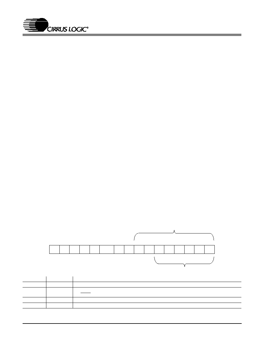
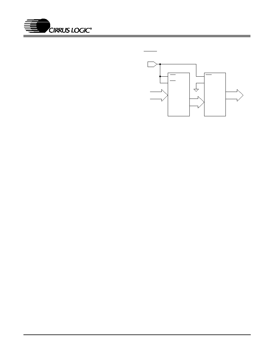
Group Header: Bits F through C of the Group
Header specify the number of words in each
group that are to be transferred to PacketPage
registers (see Figure 3.1). This value is two less
than the total number of words in the group, in-
cluding the Group Header. For example, if bits F
through C contain 0001, there are three words in
the group (a Group Header and two words of
configuration data).
Bits 9 through 0 of the Group Header specify a
10-bit PacketPage Address. This address defines
the PacketPage register that will be loaded with
the first word of configuration data from the
group. Bits B and A of the Group Header are
forced to 0, restricting the destination address
range to the first 1024 bytes of PacketPage mem-
ory.
Figure 3.1 shows the format of the Group
header.
Reset Configuration Block Checksum
A checksum is stored in the high byte position
of the word immediately following the last group
of data in the Reset Configuration Block. (The
1 0
3 2
5 4
7 6
First Word of a Group of Words
9 8
B A
D C
F E
Number of Words
in Group
0
0
10-bit PacketPage Address
Figure 3.1. Group Header
CS8920A
DS238PP2
21
EEPROM address of the checksum value can be
determined by dividing the value stored in the
Link Byte by two). The checksum value is the
2's complement of the 8-bit sum (any carry out
of eighth bit is ignored) of all the bytes in the
Reset Configuration Block, excluding the check-
s u m b yt e . T his s um i ncl ude s the Re se t
Configuration Block header at address 00h.
Since the checksum value is calculated as the 2's
complement of the sum of all the preceding
bytes in the in the Reset Configuration Block, a
total of 0 should result when the checksum value
is added to the sum of the previous bytes.
EEPROM Example
Table 3.6 shows an example of a Reset Configu-
ration Block stored in a 'C56 (non-sequential)
EEPROM. The B112h value in the header dis-
ables Plug and Play support and specifies
eighteen bytes of configuration data follow.
Note that little-endian word ordering is used, i.e.,
the least significant word of a multi-word datum
is located at the lowest address.
EEPROM Readout
If the EEDI pin is asserted high at the end of
reset, the CS8920A reads the first word of
EEPROM data by:
1. Asserting EECS
2. Clocking out a Read-Register-00h command
on EEDO (EESK provides a 1 MHz serial clock
signal)
3. Clocking the data in on EEDI.
If the EEDI pin is low at the end of the reset
signal, the CS8920A does not perform an
EEPROM readout (uses its default configura-
tion).
Determining EEPROM Size: The CS8920A de-
termines the size of the EEPROM by checking
the sense of EEDI on the tenth rising edge of
EESK. If EEDI is low, the EEPROM is a 'C46
or 'CS46. If EEDI is high, the EEPROM is a
'C56, 'CS56, 'C66, or 'CS66.
Loading Configuration Data: The CS8920A
reads in the first word from the EEPROM to de-
termine if configuration data are contained in the
F
X
E
X
D
X
C
X
B
X
ELSEL OB1 OB0
A
9
8
AD5 AD4
5
4
7
6
AD7 AD6
1
0
3
2
AD1 AD0
AD3 AD2
AD5 - AD0 used with
'C46 and 'CS46
AD7 - AD0 used with 'C56,
'CS56, 'C66 and 'CS66
Bit
Name
Description
[F:B]
Reserved
[A]
ELSEL
External Logic Select: When clear, the EECS pin is used to select the EEPROM. When set,
the ELCS pin is used to select the external LA decode circuit.
[9:8]
OB1, OB0
Opcode: Indicates what command is being executed (see next section).
[7:0]
AD7 to AD0
EEPROM Address: Address of EEPROM word being accessed.
Figure 3.2. EEPROM Command Register Format
CS8920A
22
DS238PP2
EEPROM. If configuration data are not stored in
the EEPROM, the CS8920A terminates initiali-
zation from EEPROM and operates using its
default configuration (See Table 3.3). Note: the
default configuration leaves the CS8920A in a
PnP inactive state; it can then only be accessed
through the PnP configuration and data ports. If
configuration data are stored in EEPROM, the
CS8920A automatically loads all configuration
data stored in the Reset Configuration Block into
its internal PacketPage registers.
EEPROM Readout Completion
Once all the configuration data are transferred to
the appropriate PacketPage registers, the
CS8920A adds the sum of the data bytes it read
to the 2's complement checksum at the end of
the configuration data to verify the Reset Con-
figuration Block's data are valid. If the resulting
total is 0, the readout is considered valid. Other-
wise, the CS8920A initiates a partial reset to
restore the default configuration.
If the readout is valid, the EEPROMOK bit
(Register 16, SelfST, bit A) is set. EEPROMOK
is cleared if a checksum error is detected. In this
case, the CS8920A performs a partial reset and
is restored to its default. Once initialization is
complete (configuration loaded from EEPROM
or reset to default configuration) the INITD bit is
set (Register 16, SelfST, bit 7).
3.6
Programming the EEPROM
After initialization, the host can access the
EEPROM through the CS8920A by writing one
of seven commands to the EEPROM Command
register (PacketPage base + 0040h). Figure 3.2
shows the format of the EEPROM Command
register.
EEPROM Commands
T he seven commands used to access the
EEPROM are: Read, Write, Erase, Erase/Write
Enable, Erase/Write Disable, Erase-All, and
Write-All. They are described in Table 3.7.
EEPROM Command Execution
During the execution of a command, the two Op-
code bits, followed by six bits of address (for a
'C46 or 'CS46) or eighth bits of address (for a
'C56, 'CS56, 'C66 or 'CS66), are shifted out of
the CS8920A, into the EEPROM. If the com-
mand is a Write, the data in the EEPROM Data
register (PacketPage base + 0042h) follows. If
Command
Opcode
(bits 9,8)
EEPROM Address
(bits 7 to 0)
Data
EEPROM Type
Execution Time
Read Register
1,0
word address
yes
all
25
µ
s
Write Register
0,1
word address
yes
all
10 ms
Erase Register
1,1
word address
no
all
10 ms
Erase/Write Enable
0,0
XX11-XXXX
no
'CS46, 'C46
9
µ
s
11XX-XXXX
no
'CS56, 'C56, 'CS66, 'C66
9
µ
s
Erase/Write Disable
0,0
0,0
XX00-XXXX
no
'CS46, 'C46
9
µ
s
00XX-XXXX
no
'CS56, 'C56, 'CS66, 'C66
9
µ
s
Erase-All Registers
0,0
0,0
XX10-XXXX
no
'CS46, 'C46
10 ms
10XX-XXXX
no
'CS56, 'C56, 'CS66, 'C66
10 ms
Write-All Registers
0,0
0,0
XX01-XXXX
yes
'CS46, 'C46
10 ms
01XX-XXXX
yes
'CS56, 'C56, 'CS66, 'C66
10 ms
Table 3.7. EEPROM Commands
CS8920A
DS238PP2
23
the command is a Read, the data in the specified
EEPROM location is written into the EEPROM
Data register. If the command is an Erase or
Erase-All, no data is transferred to or from the
EEPROM Data register. Before issuing any com-
mand, the host must wait for the SIBUSY bit
(Register 16, SelfST, bit 8) to clear. After each
command has been issued, the host must wait
again for SI-BUSY to clear.
Enabling Access to the EEPROM
The Erase/Write Enable command provides pro-
tection from accidental writes to the EEPROM.
The host must write an Erase/Write Enable com-
mand before it attempts to write to or erase any
EEPROM memory location. Once the host has
finished altering the contents of the EEPROM, it
must write an Erase/Write Disable command to
prevent unwanted modification of the EEPROM.
Writing and Erasing the EEPROM
To write data to the EEPROM, the host must
execute the following series of commands:
1. Issue an Erase/Write Enable command.
2. Load the data into the EEPROM Data register.
3. Issue a Write command.
4. Issue an Erase/Write Disable command.
During the Erase command, the CS8920A writes
FFh to the specified EEPROM location. During
the Erase-All command, the CS8920A writes
FFh to all locations.
3.7
Boot PROM Operation
The CS8920A supports an optional Boot PROM
used to store code for remote booting from a
network server. This is typically done for a disk-
less workstation.
Accessing the Boot PROM
The CS8920A provides address decoding cir-
cuitry to generate a chip select for a Boot
PROM. When the address on the ISA bus match
the address loaded into the Boot PROM base ad-
dress register and qualified by Boot PROM
address mask register. The CS8920A generates a
chipselect signal for the Boot PROM.
Configuring the CS8920A for Boot PROM
Operation
Figure 3.3 show how the CS8920A should be
connected to the Boot PROM and '245 driver.
To configure the CS8920A's internal registers for
Boot PROM operation, the Boot PROM Base
Address must be loaded into the Boot PROM
Base Address register (PacketPage base + 0340h)
and the Boot PROM Address Mask must be
loaded into the BootPROM Address Mask regis-
ter (PacketPage base + 0343h). The Boot PROM
Base Address provides the starting location in
host memory where the Boot PROM is mapped.
The Boot PROM Address Mask indicates the
size of the attached Boot PROM and is limited
to 4-Kbyte increments. The lower 12 bits of the
Address Mask are ignored and should be 000h.
OE
DIR
B1
.
.
.
B8
A1
.
.
.
A8
74LS245
SD(0:7)
ISA
BUS
SA(0:14)
27C256
CE
OE
20
22
19
CS8920A
CSOUT
(Pin 17)
Figure 3.3. Boot PROM Connection Diagram
CS8920A
24
DS238PP2

As an example, to configure the CS8920A to use
a 16-Kbyte (128-Kbit) PROM mapped into host
memory at a starting address of D0000h, write
0D00h to the BootPROM Base Address register
and write 0FC0h into the BootPROM Address
Mask register. (The mask value for a 16-Kbyte
PROM is 0FC00h. See Section 4.8 for more in-
formation on determing the BootPROM Address
and Mask register values.)
3.8
Low-Power Modes
For power-sensitive applications, the CS8920A
supports three low-power modes: Hardware
Standby, Hardware Suspend, and Software Sus-
pend. All three low-power modes are controlled
through the SelfCTL register (Register 15).
An internal reset occurs when the CS8920A
comes out of any suspend or standby mode. Af-
ter a reset (internal or external), the CS8920A
goes though a self configuration. This includes
calibrating on-chip analog circuitry, and reading
EEPROM for validity and configuration. When
the calibration is done, bit InitD in Register 16
(Self Status register) is set indicating that initiali-
zation is complete, and the SIBusy bit in the
same register is cleared (indicating that the
EEPROM is no longer being read or pro-
grammed. Time required for the reset calibration
is typically 10 ms. Software drivers should not
access registers internal to CS8920A during this
time.
Hardware Standby
Hardware (HW) Standby is designed for use in
systems, such as portable PC's, that may be tem-
porarily disconnected from the 10BASE-T cable.
It allows the system to conserve power while the
LAN is not in use, and then automatically re-
store Ethernet operation once the cable is
reconnected.
In HW Standby mode, all analog and digital cir-
cuitry in the CS8920A is turned off, except for
the 10BASE-T receiver which remains active to
listen for link activity. If link activity is detected,
the LANLED pin is driven low, providing an in-
dication to the host that the network connection
is active. The host can then activate the
CS8920A by de-asserting the SLEEP pin. Dur-
ing this mode, all ISA bus accesses are ignored.
CS8920A Configuration
CS8920A Operation
SLEEP
(Pin 116)
HWstandbyE
(SelfCTL, Bit
A)
HWSleepE
(SelfCTL, Bit 9)
SWSuspend
(SelfCTL, Bit 8)
Link Pulses
Low
Set
Set
Clear
Not Present
HW Standby mode:
10BASE-T receiver listens for
link activity
Low
Set
Set
Clear
Receiver
Activity
HW Standby mode:
LANLED low
Low
Clear
Set
Clear
N/A
HW Suspend mode
Low to High
N/A
Set
Clear
N/A
CS8920A resets and goes
through Initialization
High
N/A
N/A
Clear
N/A
Not in any sleep mode
Low
N/A
Clear
Set
N/A
SW Suspend mode
Low
N/A
Clear
Clear
N/A
Not in any sleep mode
NOTE: Both HW Standby and HW Suspend take precedence over SW Suspend.
Table 3.8. Low-Power Mode Operation
CS8920A
DS238PP2
25

To enter HW Standby mode, the SLEEP pin
must be low and the HWSleepE bit (Register 15,
SelfCTL, Bit 9) and the HWstandbyE bit (Regis-
ter 15, SelfCTL, Bit A) must be set. When the
CS8920A enters HW Standby, all registers and
circuits are reset except for the SelfCTL register.
Upon exit from HW Standby, the CS8920A per-
forms a complete reset, and then goes through
normal initialization.
Hardware Suspend
During Hardware Suspend mode, the CS8920A
uses the least amount of current of the three low-
power modes. All internal circuits are turned off
and the CS8920A's core is electronically isolated
from the rest of the system. Accesses from the
ISA bus and Ethernet activity are both ignored.
HW Suspend mode is entered by driving the
SLEEP pin low and setting the HWSleepE bit
(R egi ster 15, Se lfCT L, b it 9 ) whil e th e
HWstandbyE bit (Register 15, SelfCTL, bit A) is
clear. To exit from this mode, the SLEEP pin
must be driven high. Upon exit, the CS8920A
performs a complete reset, and then goes through
a normal initialization procedure.
Software Suspend
Software (SW) Suspend mode can be used to
conserve power in certain applications, such as
adapter cards that do not have power manage-
ment circuitry available. During software
suspend mode there is a partial reset. All regis-
ters and circuits are reset except for the Plug and
Play state, CSN, read data port, ISA I/O Base
Address Register, and the SelfCTL register.
To enter SW Suspend mode, the host must set
the SWSuspend bit (Register 15, SelfCTL, bit 8).
To exit SW Suspend, the host must write to the
CS8920A's assigned I/O space (the write is only
used to wake the CS8920A, the write itself is
ignored). Upon exit, the CS8920A performs a
complete reset, then goes through a normal in-
itialization procedure.
Any hardware reset takes the chip out of any
sleep mode.
Table 3.8 summarizes the operation of the three
low-power modes.
3.9
LED Outputs
The CS8920A provides four output pins that can
be used to control LEDs or external logic.
LANLED: LANLED goes low whenever the
CS8920A transmits or receives a frame, or when
it detects a collision. LANLED remains low until
there has been no activity for 6 ms (i.e. each
transmission, reception, or collision produces a
pulse lasting a minimum of 6 ms).
HC0E
(Bit C)
HCB0
(Bit E)
Pin Function
0
N/A
Pin configured as LINKLED: Output
is low when valid 10BASE-T link
pulses are detected. Output is high if
valid link pulses are not detected.
1
0
Pin configured as HC0:
Output is high
1
1
Pin configured as HC0:
Output is low
Table 3.9. LINKLED/HC0 Pin Operation
HC1E
(Bit D)
HCB1
(Bit F)
Pin Function
0
N/A
Pin configured as BSTATUS: Output
is low when a receive frame begins
transfer across the ISA bus. Output is
high otherwise.
1
0
Pin configured as HC1:
Output is high
1
1
Pin configured as HC1:
Output is low
Table 3.10. BSTATUS/HC1 Pin Operation
CS8920A
26
DS238PP2

LINKLED or HC0: LINKLED or HC0 can be
controlled by either the CS8920A or the host.
When controlled by the CS8920A, LINKLED is
low whenever the CS8920A receives valid
10BASE-T link pulses. To configure this pin for
CS8920A control, the HC0E bit (Register 15,
SelfCTL, Bit C) must be clear. When controlled
by the host, LINKLED is low whenever the
HCB0 bit (Register 15, SelfCTL, Bit E) is set.
To configure it for host control, the HC0E bit
must be set. Table 3.9 summarizes this operation.
BSTATUS or HC1: BSTATUS or HC1 can be
controlled by either the CS8920A or the host.
When controlled by the CS8920A, BSTATUS is
low whenever the host reads the RxEvent regis-
ter (PacketPage base + 0124h), signaling the
transfer of a receive frame across the ISA bus.
To configure this pin for CS8920A control, the
HC1E bit (Register 15, SelfCTL, Bit D) must be
clear. When controlled by the host, BSTATUS is
low whenever the HCB1 bit (Register 15,
SelfCTL, Bit F) is set. To configure it for host
control, HC1E must be set. Table 3.10 summa-
rizes this operation.
LOCALLED: LOCALLED goes low whenever
local LAN activity is occurring. Local LAN ac-
tivity is defined as either the the receipt of
Ethernet frames that pass the address filter of
the CS8920A, or the transmission of frames onto
the Ethernet. This LED is intended to be used
on the front panel of a PC in a manner analo-
gous to a Hard Drive Activity LED. See Section
5.3 for discussion of the receive address filter.
LED Connection
Each LED output is capable of sinking 10 mA to
drive an LED directly through a series resistor.
The output voltage of each pin is less than 0.4 V
when the pin is low. Figure 3.4 shows a typical
LED circuit.
3.10
Media Access Control
Overview
The CS8920A's Ethernet Media Access Control
(MAC) engine is fully compliant with the IEEE
802.3 Ethernet standard (ISO/IEC 8802-3, 1993).
It handles all aspects of Ethernet frame transmis-
sion and reception, including: collision detection,
preamble generation and detection, and CRC
generation and test. Programmable MAC fea-
tures include automatic retransmission on
collision, and padding of transmitted frames.
Figure 3.5 shows how the MAC engine inter-
faces to other CS8920A functions. On the host
side, it interfaces to the CS8920A's internal
+5V
LANLED
LINKLED
LOCALLED
Figure 3.4. LED Connection Diagram
802.3
MAC
Engine
Encoder/
Decoder
&
PLL
LED
Logic
CS8920A
Internal Bus
10BASE-T
& AUI
Figure 3.5. MAC Interface
CS8920A
DS238PP2
27

data/address/control bus. On the network side, it
interfaces to the internal Manchester encoder/de-
coder (ENDEC). The primary functions of the
MAC are: frame encapsulation and decapsula-
tion; error detection and handling; and, media
access management.
Frame Encapsulation and Decapsulation
The CS8920A's MAC engine automatically as-
sembles transmit packets and disassembles
receive packets. It also determines if transmit
and receive frames are of legal minimum size.
Transmission: Once the proper number of bytes
have been transferred to the CS8920A's memory
(either 5, 381, 1021 bytes, or full frame), and
providing that access to the network is permitted,
the MAC automatically transmits the 7-byte pre-
a mbl e (10 101 01b.. . ), fol lowed by th e
Start-of-Frame Delimiter (SFD, 10101011b), and
then the serialized frame data. It then transmits
the Frame Check Sequence (FCS). The data after
the SFD and before the FCS (Destination Ad-
dress, Source Address, Length, and data field) is
supplied by the host. FCS generation by the
CS8920A may be disabled by setting the In-
hibitCRC bit (Register 9, TxCMD, bit C).
Figure 3.6 shows the Ethernet frame format.
Reception: The MAC receives the incoming
packet as a serial stream of NRZ data from the
Manchester encoder/decoder. It begins by check-
ing for the SFD. Once the SFD is detected, the
MAC assumes all subsequent bits are frame data.
It reads the DA and compares it to the criteria
programmed into the address filter (see Section
5.3 for a description of Address Filtering). If the
DA passes the address filter, the frame is loaded
into the CS8920A's memory. If the BufferCRC
bit (Register 3, RxCFG, bit B) is set, the re-
ceived FCS is also loaded into memory. Once
the entire packet has been received, the MAC
validates the FCS. If an error is detected, the
CRCerror bit (Register 4, RxEvent, Bit C) is set.
Enforcing Minimum Frame Size: The MAC
provides minimum frame size enforcement of
both transmit and receive packets. When the
TxPadDis bit (Register 9, TxCMD, Bit D) is
clear, transmit frames will be padded with addi-
tional bits to ensure that the receiving station
receives a legal frame (64 bytes, including
CRC). When TxPadDis is set, the CS8920A will
not add pad bits and will transmit frames less
that 64 bytes. If a frame is received that is less
than 64 bytes (including CRC), the Runt bit
(Register 4, RxEvent, Bit D) will be set indicat-
ing the arrival of an illegal frame.
1 byte
up to 7 bytes
6 bytes
6 bytes
2 bytes N bytes M bytes
LLC data
Pad
FCS
4 bytes
preamble
frame length
min 64 bytes
max 1518 bytes
alternating 1s / 0s
SFD
DA
SA
The optional field, which is two bytes long, is
either a TYPE field for Ethernet applications or
a LENGTH field for IEEE 802.3 applications.
The Pad field will be used only to get the frame
to the minimum size. When the CS8920 adds pad
bytes, the pad is the last byte of the LLC data
field repeated M times.
Direction of Transmission
Frame
Packet
Optional Field
SFD = Start of Frame Delimiter
DA = Destination Address
SA = Source Address
LLC = Logical Link Control
FCS = Frame Check Sequence (also
called Cyclic Redundancy Check, or CRC)
Figure 3.6. Ethernet Frame Format
CS8920A
28
DS238PP2

Transmit Error Detection and Handling
The MAC engine monitors Ethernet activity and
reports and recovers from a number of error con-
ditions. For transmission, the MAC reports the
following errors in the TxEvent register (Register
8) and BufEvent register (Register C):
Loss of Carrier: Whenever the CS8920A is
transmitting on the AUI port, it expects to see its
own transmission "looped back" to its receiver. If
it is unable to monitor its transmission after the
end of the preamble, the MAC reports a loss-of-
carrier error by setting the Loss-of-CRS bit
(Register 8, TxEvent, Bit 6). If the Loss-of-
CRSiE bit (Register 7, TxCFG, Bit 6) is set, the
host will be interrupted.
SQE Error: After the end of transmission on the
AUI port, the MAC expects to see a collision
within 64 bit times. If no collision is detected,
the SQEerror bit (Register 8, TxEvent, Bit 7) is
set. If the SQEerroriE bit is set (Register 7,
TxCFG, Bit 7), the host is interrupted. An SQE
error may indicate a fault on the AUI cable or a
faulty transceiver (it is assumed that the attached
transceiver supports this function).
Out-of-Window (Late) Collision: If a collision is
detected after the first 512 bits have been trans-
mitted, the MAC reports a late collision by
setting the Out-of-window bit (Register 8,
TxEvent, Bit 9). The MAC then forces a bad
CRC and terminates the transmission. If the Out-
of-windowiE bit (Register 7, TxCFG, Bit 9) is
set, the host is interrupted. A late collision may
indicate an illegal network configuration.
Jabber Error: If a transmission continues longer
than about 26 ms, the MAC disables the trans-
mitter and sets the Jabber bit (Register 8,
TxEvent, Bit A). The output of the transmitter
returns to idle and remains there until the host
issues a new Transmit Command. If the JabberiE
bit (Register 7, TxCFG, Bit A) is set, the host is
interrupted. A Jabber condition indicates that
t here may be so me thi ng wrong with the
CS8920A transmit function. To prevent possible
network faults, the host should clear the transmit
buffer. Possible options include:
Reset the chip with either software or hardware
reset (see Section 3.3).
Issue a Force Transmit Command by setting the
Force bit (Register 9, TxCMD, bit 8).
Issue a Transmit Command with the TxLength
field set to zero.
Transmit Collision: The MAC counts the num-
ber of times an individual packet must be
re-transmitted due to network collisions. The col-
lision count is stored in bits B through E of the
TxEvent register (Register 8). If the packet col-
lides 16 times, transmission of that packet is
terminated and the 16coll bit (Register 8,
TxEvent, Bit F) is set. If the 16colliE bit (Regis-
ter 7, TxCFG, Bit F) is set, the host will be
interrupted on the 16th collision. A running
count of transmit collisions is recorded in the
TxCOL register.
Transmit Underrun: If the CS8920A starts
transmission of a packet but runs out of data be-
fore reaching the end of frame, the TxUnderrun
bit (Register C, BufEvent, Bit 9) is set. The
MAC then forces a bad CRC and terminates the
transmission. If the TxUnderruniE bit (Register
B, BufCFG, Bit 9) is set, the host is interrupted.
Receive Error Detection and Handling
The following receive errors are reported in the
RxEvent register (Register 4):
CRC Error: If a frame is received with a bad
CRC, the CRCerror bit (Register 4, RxEvent, Bit
C) is set. If the CRCerrorA bit (Register 5,
RxCTL, Bit C) is set, the frame will be buffered
by the CS8920A. If the CRCerroriE bit (Register
3, RxCFG. Bit C) is set, the host is interrupted.
CS8920A
DS238PP2
29

Runt Frame: If a frame is received that is
shorter than 64 bytes, the Runt bit (Register 4,
RxEvent, Bit D) is set. If the RuntA bit (Register
5, RxCTL, Bit D) is set, the frame will still be
buffered by CS8920A. If the RuntiE bit (Regis-
ter 3, RxCFG. Bit D) is set, the host is
interrupted.
Extra Data: If a frame is received that is longer
than 1518 bytes, the Extradata bit (Register 4,
RxEvent, Bit E) is set. If the ExtradataA bit
(Register 5, RxCTL, Bit E) is set, the first 1518
bytes of the frame will still be buffered by
CS8920A. If the ExtradataiE bit (Register 3,
RxCFG. Bit E) is set, the host is interrupted.
Dribble Bits and Alignment Error: Under nor-
mal operating conditions, the MAC may detect
up to 7 additional bits after the last full byte of a
receive packet. These bits, known as dribble bits,
are ignored. If dribble bits are detected, the Drib-
blebit bit (Register 4, RxEvent, Bit 7) is set. If
both the Dribblebit bit and CRCerror bit (Regis-
ter 4, RxEvent, Bit C) are set at the same time,
an alignment error has occurred.
Media Access Management
The Ethernet network topology is a single shared
medium with several attached stations. The Eth-
ernet protocol is designed to allow each station
equal access to the network at any given time.
Any node can attempt to gain access to the net-
work by first completing a deferral process
(described below) after the last network activity,
and then transmitting a packet that will be re-
ceived by all other stations. If two nodes
transmit simultaneously, a collision occurs and
the colliding packets are corrupted. Two primary
tasks of the MAC are to avoid network colli-
sions, and then recover from them when they
occur. In addition, when the CS8920A is using
the AUI, the MAC must support the SQE Test
function described in section 7.2.4.6 of the Eth-
ernet standard.
Collision Avoidance: The MAC continually
monitors network traffic by checking for the
presence of carrier activity (carrier activity is in-
dicated by the assertion of the internal Carrier
Sense signal generated by the ENDEC). If car-
rier activity is detected, the network is assumed
busy and the MAC must wait until the current
packet is finished before attempting transmis-
sion. The CS8920A supports two schemes for
determining when to initiate transmission: Two-
Part Deferral, and Simple Deferral. Selection of
the deferral scheme is determined by the 2-part-
Transmit
Frame
Start Monitoring
Network Activity
IPG
Timer =
6.4
µ
s?
Network
Active?
Network
Active?
Start IPG
Timer
Network
Active?
Yes
No
Yes
Yes
Yes
No
No
No
No
Wait
3.2
µ
s
Yes
Tx
Frame
Ready
and
Not
in Backoff?
Figure 3.7. Two-Part Deferral
CS8920A
30
DS238PP2

DefDis bit (Register 13, LineCTL, Bit D). If the
2-partDefDis bit is clear, the MAC uses a two-
part deferral process defined in section 4.2.3.2.1
of the Ethernet standard (ISO/IEC 8802-3,
1993). If the 2-partDefDis bit is set, the MAC
uses a simplified deferral scheme. Both schemes
are described below:
Two-Part Deferral: In the two-part deferral proc-
ess, the 9.6
µ
s Inter Packet Gap (IPG) timer is
started whenever the internal Carrier Sense sig-
nal is de-asserted. If activity is detected during
the first 6.4
µ
s of the IPG timer, the timer is re-
set and then restarted once the activity has
stopped. If there is no activity during the first 6.4
µ
s of the IPG timer, the IPG timer is allowed to
time out (even if network activity is detected
during the final 3.2
µ
s). The MAC then begins
transmission if a transmit packet is ready and if
it is not in Backoff (Backoff is described later in
this section). If no transmit packet is pending,
the MAC continues to monitor the network. If
activity is detected before a transmit frame is
ready, the MAC defers to the transmitting station
and resumes monitoring the network.
The two-part deferral scheme was developed to
prevent the possibility of the IPG being short-
ened due to a temporary loss of carrier. Figure
3.7 diagrams the two-part deferral process.
Simple Deferral: In the simple deferral scheme,
the IPG timer is started whenever Carrier Sense
is de-asserted. Once the IPG timer is finished
(after 9.6
µ
s), if a transmit frame is pending and
if the MAC is not in Backoff, transmission be-
gins (even if network activity is detected during
the 9.6
µ
s IPG). If no transmit packet is pending,
the MAC continues to monitor the network. If
activity is detected before a transmit frame is
ready, the MAC defers to the transmitting station
and resumes monitoring the network. Figure 3.8
diagrams the simple deferral process.
Collision Resolution: If a collision is detected
while the CS8920A is transmitting, the MAC re-
sponds in one of three ways depending on
whether it is a normal collision (within the first
512 bits of transmission) or a late collision (after
the first 512 bits of transmission):
Normal Collisions: If a collision is detected be-
fore the end of the preamble and SFD, the MAC
finishes the preamble and SFD, transmits the jam
sequence (32-bit pattern of all 0's), and then in-
itiates Backoff. If a collision is detected after the
transmission of the preamble and SFD but before
512 bit times, the MAC immediately terminates
transmission, transmits the jam sequence, and
then initiates Backoff. In either case, if the
Onecoll bit (Register 9, TxCMD, Bit 9) is clear,
the MAC will attempt to transmit a packet a total
of 16 times (the initial attempt plus 15 retrans-
missions) due to normal collisions. On the 16th
collision, it sets the 16coll bit (Register 8,
TxEvent, Bit F) and discards the packet. If the
Tx
Frame
Ready
and
Not
in Backoff?
Transmit
Frame
Start Monitoring
Network Activity
Network
Active?
Network
Active?
Yes
No
Yes
No
No
Yes
Wait
9.6
µ
s
Figure 3.8. Simple Deferral
CS8920A
DS238PP2
31
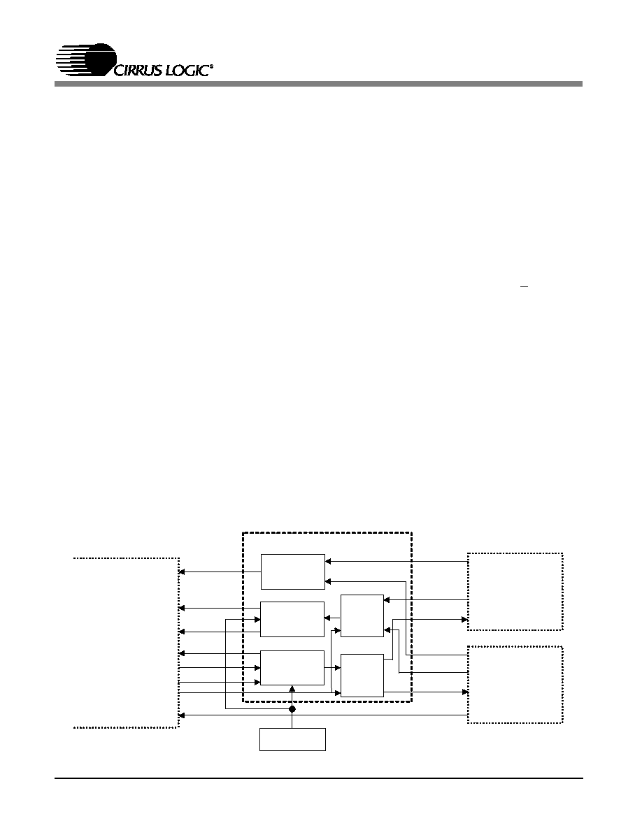
Onecoll bit is set, the MAC discards the packet
without attempting any re-transmission.
Late Collisions: If a collision is detected after
the first 512 bits have been transmitted, the
MAC immediately terminates transmission,
transmits the jam sequence, discards the packet,
and sets the Out-of-window bit (Register 8,
TxEvent, Bit 9). The CS8920A does not initiate
backoff or attempt to re-transmit the frame. For
additional information about Late Collisions, see
Out-of-Window Error in this section.
Backoff: After the MAC has completed transmit-
ting the jam sequence, it must wait, or "Back
off", before attempting to transmit again. The
amount of time it must wait is determined by
one of two Backoff algorithms: the Standard
Backoff algorithm (ISO/IEC 4.2.3.2.5) or the
Modified Backoff algorithm. The host selects
which algorithm through the ModBackoffE bit
(Register 13, LineCTL, Bit B).
Standard Backoff: The Standard Backoff algo-
rithm, also called the "Truncated Binary
Exponential Backoff", is described by the equa-
tion:
0
r
2
k
where r (a random integer) is the number of slot
times the MAC must wait (1 slot time = 512 bit
times), and k is the smaller of n or 10, where n
is the number of re-transmission attempts.
Modified Backoff: The Modified Backoff is de-
scribed by the equation:
0
r
2
k
where r (a random integer) is the number of slot
times the MAC must wait, and k is 3 for n <3
and k is the smaller of n or 10 for n>3, where n
is the number of re-transmission attempts.
The advantage of the Modified Backoff algo-
rithm over the Standard Backoff algorithm is that
it reduces the possibility of multiple collisions
on the first three re-tries. The disadvantage is
that it extends the maximum time needed to gain
access to the network for the first three re-tries.
The host may choose to disable the Backoff al-
gorithm altogether by setting the DisableBackoff
bit (Register 19, TestCTL, Bit B). When dis-
abled, the CS8920A only waits the 9.6
µ
s IPG
time before starting transmission.
Encoder
Carrier
Detector
Decoder
& PLL
RX
MUX
TX
MUX
RXSQL
AUISQL
RX
TX
AUIRX
AUITX
AUICol
Clock
Carrier Sense
RX CLK
RX NRZ
TXCLK
TX NRZ
TEN
Port Select
Collision
MAC
ENDEC
10BASE-T
Transceiver
AUI
Figure 3.9. ENDEC
CS8920A
32
DS238PP2

SQE Test: If the CS8920A is transmitting on the
AUI, the external transceiver should generate an
SQE Test signal on the CI+/CI- pair following
each transmission. The SQE Test is a 10 MHz
signal lasting 5 to 15 bit times and starting
within 0.6 to 1.6
µ
s after the end of transmis-
sion. During this period, the CS8920A ignores
receive carrier activity (see SQE Error in this
section for more information).
3.11
Encoder/Decoder (ENDEC)
The CS8920A's integrated encoder/decoder (EN-
DEC) circuit is compliant with the relevant
portions of section 7 of the Ethernet standard
(ISO/IEC 8802-3, 1993). Its primary functions
include:
Manchester encoding of transmit data;
informing the MAC when valid receive data is
present (Carrier Detection); and, recovering the
clock and NRZ data from incoming Manchester-
encoded data.
Figure 3.9 provides a block diagram of the EN-
DEC and how it interfaces to the MAC, AUI and
10BASE-T transceiver.
Encoder
The encoder converts NRZ data from the MAC
and a 20 MHz Transmit Clock signal into a se-
rial stream of Manchester data. The Transmit
Clock is produced by an on-chip oscillator cir-
cuit that is driven by either an external 20 MHz
quartz crystal or a TTL-level CMOS clock input.
If a CMOS input is used, the clock should be 20
MHz
±
0.01% with a duty cycle between 40%
and 60%. The specifications for the crystal are
described in section 13.0 (Quartz Crystal Re-
quirements). The encoded signal is routed to
either the 10BASE-T transceiver or AUI, de-
pending on configuration.
Carrier Detection
The internal Carrier Detection circuit informs the
MAC that valid receive data is present by assert-
ing the internal Carrier Sense signal as soon it
detects a valid bit pattern (1010b or 0101b for
10BASE-T, and 1b or 0b for AUI). During nor-
mal packet reception, Carrier Sense remains
asserted while the frame is being received, and is
de-asserted 1.3 to 2.3 bit times after the last low-
to-high transition of the End-of-Frame (EOF)
sequence. Whenever the receiver is idle (no re-
ceive activity), Carrier Sense is de-asserted. The
CRS bit (Register 14, LineST, Bit E) reports the
state of the Carrier Sense signal.
Clock and Data Recovery
When the receiver is idle, the phase-lock loop
(PLL) is locked to the internal clock signal. The
assertion of the Carrier Sense signal interrupts
the PLL. When it restarts, it locks on the incom-
ing data. The receive clock is then compared to
the incoming data at the bit cell center and any
phase difference is corrected. The PLL remains
locked as long as the receiver input signal is
valid. Once the PLL has locked on the incoming
data, the ENDEC converts the Manchester data
to NRZ and passes the decoded data and the re-
covered clock to the MAC for further processing.
Interface Selection
Physical interface selection is determined by the
AUIonly bit (Bit 8) and the AutoAUI/10BT bit
(Bit 9) in the LineCTL register (Register 13).
Table 3.11 describes the possible configurations.
AUIonly
(Bit 8)
AutoAUI/10BT
(Bit 9)
Physical
Interface
0
0
10BASE-T Only
1
N/A
AUI Only
0
1
Auto-Select
Table 3.11. Interface Selection
CS8920A
DS238PP2
33

10BASE-T Only: When configured for 10BASE-
T-only operation, the 10BASE-T transceiver and
its interface to the ENDEC are active, and the
AUI is powered down.
AUI Only: When configured for AUI-only opera-
tion, the AUI and its interface to the ENDEC are
active, and the 10BASE-T transceiver is powered
down.
Auto-Select: In Auto-Select mode, the CS8920A
automatically selects the 10BASE-T interface
and powers down the AUI if valid packets or link
pulses are detected by the 10BASE-T receiver. If
valid packets and link pulses are not detected,
the CS8920A selects the AUI. Whenever the AUI
is selected, the 10BASE-T receiver remains ac-
tive to listen for link pulses or packets. If
10BASE-T activity is detected, the CS8920A
switches back to 10BASE-T.
3.12
10BASE-T Transceiver
The CS8920A includes an integrated 10BASE-T
transceiver that is compliant with the relevant
portions of section 14 of the Ethernet standard
(ISO/IEC 8802-3, 1993). It includes all analog
and digital circuitry needed to interface the
CS8920A directly to a simple isolation trans-
former (see section 11.0 for a connection
diagram). Figure 3.10 provides a block diagram
of the 10BASE-T transceiver.
10BASE-T Filters
The CS8920A's 10BASE-T transceiver includes
integrated low-pass transmit and receive filters,
eliminating the need for external filters or a fil-
ter/transformer hybrid. On-chip filters are gm/c
implementations of fifth-order Butterworth low-
pass filters. Internal tuning circuits keep the
gm/c ratio tightly controlled, even when large
temperature, supply, and IC process variations
RXSQL
RX
TX
Link Pulse
Detector
TX Pre-
Distortion
RX Squelch
RX
Comparator
TX Filters
Filter Tuning
RX Filters
TX Drivers
RXD-
RXD+
TXD-
TXD+
ENDEC
LinkOK
(to MAC)
10BASE-T Transceiver
Figure 3.10. 10BASE-T Transceiver
CS8920A
34
DS238PP2

occur. The nominal 3 dB cutoff frequency of the
filters is 16 MHz, and the nominal attenuation at
30 MHz (3rd harmonic) is -27 dB.
Transmitter
When configured for 10BASE-T operation, Man-
chester encoded data from the ENDEC is fed
into the transmitter's pre-distortion circuit where
initial wave shaping and pre-equalization is per-
formed. The output of the pre-distortion circuit is
fed into the transmit filter where final wave
shaping occurs and unwanted noise is removed.
The signal then passes to the differential driver
where it is amplified and driven out of the
TXD+/TXD- pins.
In the absence of transmit packets, the transmit-
ter generates link pulses in accordance with
section 14.2.1.1 of the Ethernet standard. Trans-
mitted link pulses are positive pulses, one bit
time wide, typically generated at a rate of one
every 16 ms. The 16 ms timer starts whenever
the transmitter completes an End-of-Frame
(EOF) sequence. Thus, there is a link pulse 16
ms after an EOF unless there is another transmit-
ted packet. Figure 3.11 diagrams the operation of
the Link Pulse Generator.
If no link pulses are being received on the re-
ceiver, the 10BASE-T transmitter is internally
forced to an inactive state unless bit DisableLT
in register 19 (Test Control register) is set to one.
Receiver
The 10BASE-T receive section consists of the
receive filter, squelch circuit, polarity detection
and correction circuit, and link pulse detector.
Squelch Circuit: The 10BASE-T squelch circuit
determines when valid data is present on the
RXD+/RXD- pair. Incoming signals passing
through the receive filter are tested by the
squelch circuit. Any signal with amplitude less
than the squelch threshold (either positive or
negative, depending on polarity) is rejected.
Extended Range: The CS8920A supports an Ex-
tended Range feature that reduces the 10BASE-T
receive squelch threshold by approximately 6
dB. This allows the CS8920A to operate with
10BASE-T cables that are longer than 100 me-
ters (100 meters is the maximum length specified
by the Ethernet standard). The exact additional
distance depends on the quality of the cable and
the amount of electro-magnetic noise in the sur-
rounding environment. To activate this feature,
the host must set the LoRxSquelch bit (Register
13, LineCTL, Bit E).
Auto-Negotiation
The CS8920A supports Auto-Negotiation, the
mechanism that allows the two devices on either
end of a 10Base-T link segment to share infor-
mation and automatically configure both devices
for maximum performance. When configured for
Auto-Negotiation, the CS8920A will detect and
automatically operate full-duplex, if the device
on the other end of the link segment also sup-
ports full-duplex and Auto-Negotiation. The
CS8920A Auto-Negotiation capability is fully
compliant with the relevant portions of section
28 of the IEEE 802.3u standard.
Auto-Negotiation encapsulates information
within a burst of closely spaced link integrity
test pulses, referred to as a Fast Link Pulse
(FLP) Burst. The FLP Burst consists of a series
of link integrity pulses which form an alternating
clock / data sequence. Extraction of the data bits
from the FLP Burst yields a Link Code Word
which identifies the capability of the remote de-
vice. To remain interoperable with existing
10Base-T devices, the CS8920A also supports
the reception of 10Base-T compliant link integ-
rity test pulses, refered to as Normal Link Pulses
(NLP). Devices that respond to the CS8920A
with a Normal Link Pulse, cause the CS8920A
to operate as a 10Base-T half-duplex device.
CS8920A
DS238PP2
35
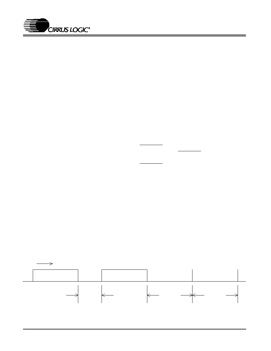
Prior to enabling Auto-Negotiation, the Al-
lowFDX bit (Register 1D, AutoNegCTL, Bit 7)
should be set if full-duplex operation is to be al-
lowed and reset otherwise. If this bit is reset,
only half-duplex operation will be negotiated.
To enable Auto-Negotiation the host should set
t he Au toNegE nab le bit (Registe r 1D,
AutoNegCTL, Bit 8) and reset the NLPEnable
bit (Register 1D, AutoNegCTL, Bit 9) and the
ForceFDX bit (Register 1D, AutoNegCTL, Bit
F).
Re-negotiation can be forced to occur by setting
the ReNOW bit (Register 1D, AutoNegCTL, bit
6). Typically, this is done after a change in the
settings of the Auto-Negotiation bits, in order to
cause the new settings to be acted upon.
The NLPEnable bit (Register 1D, AutoNegCTL,
bit 9) overrides the Auto-Negotiation settings
and causes Normal Link Pulses to be transmitted
by the CS8920A. Auto-Negotiation is disabled.
The following section describes the operation of
the CS8920A in NLP mode.
Link Pulse Detection
To prevent disruption of network operation due
to a faulty link segment, the CS8920A continu-
ally monitors the 10BASE-T receive pair
(RXD+/ RXD-) for packets and link pulses. Af-
ter each packet or link pulse is received, an
internal Link-Loss timer is started. As long as a
packet or link pulse is received before the Link-
Loss timer finishes (between 25 and 150 ms),
the CS8920A maintains normal operation. If no
receive activity is detected, the CS8920A dis-
ables packet transmission to prevent "blind"
transmissions onto the network (link pulses are
still sent while packet transmission is disabled).
To reactivate transmission, the receiver must de-
tect a single packet (the packet itself is ignored),
or two link pulses separated by more than 2 to 7
ms and no more than 25 to 150 ms (see section
10.0 for 10BASE-T timing).
The state of the link segment is reported in the
LinkOK bit (Register 14, LineST, Bit 7). If the
HC0E bit (Register 15, SelfCTL, Bit C) is clear,
it is also indicated by the output of the
LINKLED pin. If the link is "good", the LinkOK
bit is set and the LINKLED pin is driven low. If
the link is "bad" the LinkOK bit is clear and the
LINKLED pin is high. To disable this feature,
the host must set the DisableLT bit (Register 19,
TestCTL, Bit 7). If DisableLT is set, the
CS8920A will transmit and receive packets inde-
pendent of the link segment.
Receive Polarity Detection and Correction
The CS8920A automatically checks the polarity
of the receive half of the twisted pair cable. If
the polarity is correct, the PolarityOK bit (Regis-
ter 14, LineST, bit C) is set. If the polarity is
reversed, the PolarityOK bit is clear. If the Polar-
ityDis bit (Register 13, LineCTL, Bit C) is clear,
Packet
less than
16 ms
16 ms
16 ms
Link
Pulse
Link
Pulse
Time
Packet
Figure 3.11. Link Pulse Transmission
CS8920A
36
DS238PP2
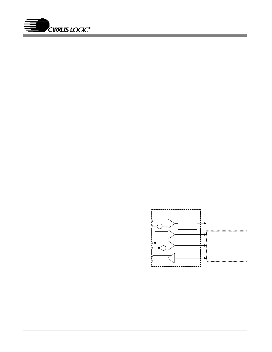
the CS8920A automatically corrects a reversal. If
the PolarityDis bit is set, the CS8920A does not
correct a reversal. The PolarityOK bit and the
PolarityDis bit are independent.
To detect a reversed pair, the receiver examines
received link pulses and the End-of-Frame
(EOF) sequence of incoming packets. If it de-
tects at least one reversed link pulse and at least
four frames in a row with negative polarity after
the EOF, the receive pair is considered reversed.
Any data received before the correction of the
reversal is ignored.
Collision Detection
If half-duplex operation is selected (Register 1D,
Bit E, ForceFDX), the CS8920A detects a
10BASE-T collision whenever the receiver and
transmitter are active simultaneously. When a
collision is present, the Collision Detection cir-
cuit informs the MAC by asserting the internal
Collision signal (see section 3.11 for collision
handling).
3.13
Attachment Unit Interface (AUI)
The CS8920A Attachment Unit Interface (AUI)
provides a direct interface to external 10BASE2,
10BASE5, and 10BASE-FL Ethernet transceiv-
ers. It is fully compliant with Section 7 of the
Ethernet standard (ISO/IEC 8802-3), and as
such, is capable of driving a full 50-meter AUI
cable.
The AUI consists of three pairs of signals: Data
Out (DO+/DO-), Data In (DI+/DI-), and Colli-
sion In (CI+/CI-). To select the AUI, the host
should set the AUI bit (Register 13, LineCTL,
Bit 8). The AUI can also be selected automat-
ically as described in the previous section.
Figure 3.12 provides a block diagram of the
AUI. (For a connection diagram, see section
12.0).
AUI Transmitter
The AUI transmitter is a differential driver de-
signed to drive a 78 ohm cable. It accepts data
from the ENDEC and transmits it directly on the
DO+/DO- pins. After transmission has started,
the CS8920A expects to see the packet "looped-
back" (or echoed) to the receiver, causing the
Carrier Sense signal to be asserted. This Carrier
Sense presence indicates that the transmit signal
is getting through to the transceiver. If the Car-
rier Sense signal remains de-asserted throughout
the transmission, or if the Carrier Sense signal is
de-asserted before the end of the transmission,
there is a Loss-of-Carrier error and the Loss-of-
CRS bit (Register 8, TxEvent, Bit 6) is set.
AUI Receiver
The AUI receiver is a differential pair circuit that
connects directly to the DI+/DI- pins. It is de-
signed to distinguish between transient noise
pulses and incoming Ethernet packets. Incoming
packets with proper amplitude and pulse width
are passed on to the ENDEC section, while un-
wanted noise is rejected.
Collision Detection
The AUI collision circuit is a differential pair re-
ceiver that detects the presence of collision
signals on the CI+/CI- pins. The collision signal
is generated by an external Ethernet transceiver
whenever a collision is detected on the Ethernet
DI+
DI-
DO+
DO-
ENDEC
CI+
CI-
Collision
Detect
AUICol (to MAC)
AUIRX
AUISQL
AUITX
AUI
- +
- +
Figure 3.12. AUI
CS8920A
DS238PP2
37

segment. (Section 7.3.1.2 of ISO/IEC 8802-3,
1993, defines the collision signal as a 10 MHz
+/- 15% signal with a duty cycle no worse than
60/40). When a collision is present, the AUI Col-
lision circuit informs the MAC by asserting the
internal Collision signal.
3.14
External Clock Oscillator
A 20 MHz quartz crystal or CMOS clock input
is required by the CS8920A. If a CMOS clock
input is used, it should be connected the to
XTAL1 pin, with the XTAL2 pin left open. The
clock signal should be 20 MHz
±
0.01% with a
duty cycle between 40% and 60%. The specifi-
cations for the crystal are described in section
13.0 (Quartz Crystal Requirements).
CS8920A
38
DS238PP2

4.0
PACKETPAGE ARCHITECTURE
4.1
PacketPage Overview
The CS8920A architecture is based on a unique,
highly-efficient method of accessing internal reg-
isters and buffer memory known as PacketPage.
PacketPage provides a unified way of controlling
the CS8920A in Memory or I/O space that mini-
mizes CPU overhead and simplifies software. It
provides a flexible set of performance features
and configuration options, allowing designers to
develop Ethernet circuits that meet their particu-
lar system requirements.
Integrated Memory
Central to the CS8920A architecture is a 4-Kbyte
page of integrated RAM known as PacketPage
memory. PacketPage memory is used for tempo-
rary storage of transmit and receive frames, and
for internal registers. Access to this memory is
done directly, through Memory space operations
(Section 4.11), or indirectly, though I/O space
operations (Section 4.12). In most cases, Mem-
o ry Mod e will p rovi de the be st overal l
performance, because ISA Memory operations
require fewer cycles than I/O operations. I/O
Mode is the CS8920A's default configuration and
is used when memory space is not available or
when special operations are required (e.g. wak-
ing the CS8920A from the Software Sleep state
requires the host to write to the CS8920A's as-
signed I/O space).
The user-accessible portion of PacketPage mem-
ory is organized into the following sections:
Bus Interface Registers
The Bus Interface registers are used to configure
the CS8920A's ISA-bus interface and to map the
CS8920A into the host system's I/O and Mem-
ory space. Most of these registers are written
only during initialization, remaining unchanged
while the CS8920A is in normal operating mode.
The exceptions to this are the DMA registers
which are modified continually whenever the
CS8920A is using DMA. These registers are de-
scribed in more detail in Section 4.3.
Status and Control Registers
The Status and Control registers are the primary
means of controlling and getting status of the
CS8920A. They are described in more detail in
Section 4.4.
Initiate Transmit Registers
The TxCMD/TxLength registers are used to initi-
ate Ethernet frame transmission. These registers
are described in more detail in Section 4.6. (See
Section 5.8 for a description of frame transmis-
sion.)
Address Filter Registers
The Filter registers store the Individual Address
filter and Logical Address filter used by the Des-
tination Address (DA) filter. These registers are
described in more detail in Section 4.7. For a de-
scription of the DA filter, see Section 5.3.
Plug and Play Registers
Plug and Play registers hold resources assigned
by a plug and play configuration manager. These
resources include IO and memory base address,
interrupt number and DMA channel. See section
4.8.
PacketPage
Address
Contents
0000h - 0048h
Product/Bus Specific Registers
0100h - 013Fh
Status and Normal Control Registers
0120h
Interrupt Status Queue
0140h - 015Dh
Ethernet, or Line, Related Registers
0330h - 03FFh
Plug and Play Registers
0400h - 09FFh
Current Receive Frame Virtual Map
0A00h - 0FFFh
Current Transmit Frame Virtual Map
CS8920A
DS238PP2
39

Receive and Transmit Frame Locations
The Receive and Transmit Frame PacketPage lo-
cations are used to transfer Ethernet frames to
and from the host. The host simply writes to and
reads from these locations, and internal buffer
memory is dynamically allocated between trans-
mit and receive as needed. This provides more
efficient use of buffer memory and better overall
network performance. As a result of this dynamic
allocation, only one receive frame (starting at
PacketPage base + 0400h) and one transmit
frame (starting at PacketPage base + 0A00h) are
directly accessible. See Section 4.9.
4.2
PacketPage Memory Map
Table 4.1 shows the CS8920A PacketPage mem-
ory address map:
Table 4.1 is continued on the next page.
Base
+
# of
Bytes
Type
Description
Cross
Reference
Bus Interface Registers
0000h
4
Read-only
32-bit Product Identification Code
Section 4.3
0004h
34
Reserved
Note 2
0026h
2
Read-only
ISA RxDMA Start of Frame 16-bit Offset to Status
Sections 4.3, 4.12
0028h
2
Read-only
ISA RxDMA 12-bit Frame Count
Sections 4.3
002Ah
2
Read-only
ISA RxDMA Byte Count 16 bit
Sections 4.3
002Ch
20
Reserved. Do Not Write to This Space.
Note 2
0040h
2
Read/Write
EEPROM Command Register
Sections 3.6, 4.3
0042h
2
Read/Write
EEPROM Data Word
Sections 3.6, 4.3
0044h
4
Reserved. Do Not Write to This Space.
Note 2
0048h
2
Read
Link Partner Ability in Auto Negotiation
Note 2
004Ah
6
Read/Write
Reserved. Do Not Write to This Space.
Sections 3.6, 4.3
0050h
2
Read-only
Receive Frame byte counter
Sections 4.3, 5.2.9
0052h
174
Reserved
Note 2
Status and Control Registers
0100h
32
CS8920A Config/Control Registers (two bytes per coded
value)
Section 4.4, 4.5
0120h
32
CS8920A Status/Event Registers, ISQ is 0120h
Section 4.4, 4.5
0140h
2
Read-only
Reserved. Do Not Use.
Note 2
0142h
2
Reserved. Do Not Write to This Space.
Note 2
NOTES:
1) All registers are accessed as words only.
2) Read operation from the reserved location provides undefined data. Writing to a reserved location or
undefined bits may result in unpredictable operation of the CS8920A.
Table 4.1. PacketPage Memory Address Map
CS8920A
40
DS238PP2

Base
+
# of
Bytes
Type
Description
Cross
Reference
Initiate Transmit Registers
0144h
2
Read/Write
TxCMD. Command Request. The Value Written Here is Shown
in registert 9.
Sections 4.6, 5.8
0146h
2
Read/Write
TxLength. Command Length Request in Bytes.
Sections 4.6, 5.8
0148h
8
Reserved
Note 2
Address Filter Registers
0150h
8
Read/Write
Logical Address Filter (hash table)
Sections 4.7, 5.3
0158h
6
Read/Write
Individual Address, IA
Sections 4.7, 5.3
015E
674
Reserved. Do Not Write in This Space.
Note 2
Frame Location
0330h
1
Read/Write
PNP Activation Register
Sections 4.8
0331h
1
Read/Write
PNP IO Range Check Register
Sections 4.8
0340h
1
Read/Write
Boot PROM Base Address, high byte
Sections 4.8
0341h
1
Read/Write
Boot PROM Base Address, low byte
Sections 4.8
0343h
1
Read/Write
Boot PROM Address Mask, high byte A(23:16)
Sections 4.8
0344h
1
Read/Write
Boot PROM Address Mask, low byte A(15:8)
Sections 4.8
0348h
1
Read/Write
Memory Base Address, high byte
Sections 4.8
0349h
1
Read/Write
Memory Base Address, low byte
Sections 4.8
0360h
1
Read/Write
IO Base Address, high byte
Sections 4.8
0361h
1
Read/Write
IO Base Address, low byte
Sections 4.8
0370h
1
Read/Write
Interrupt Request Channel Select 0
Sections 4.8
0371h
1
Read Only
Interrupt Request Type Select 0
Sections 4.8
0374h
1
Read/Write
DMA Channel Select
Sections 4.8
0400h
2
Read Only
Receive Status
Sections 4.9, 5.8
0402h
2
Read Only
Receive Length
Sections 4.9, 5.8
0404h
Aliased RxFrame
Sections 4.9, 5.8
0A00h
Aliased TxFrame
Sections 4.9, 5.8
NOTES:
1. All registers are accessed as words only.
2. Read operation from the reserved location provides undefined data. Writing to a reserved location or
undefined bits may result in unpredictable operation of the CS8920A.
Table 4.1. PacketPage Memory Address Map, continued
CS8920A
DS238PP2
41

4.3
Bus Interface Registers
Bus Interface Register:
Product Identification Code (Read only)
Address: PacketPage base + 0000h
Address 0000h
Address 0001h
Address 0002h
Address 0003h
First byte of EISA registration
number for
Crystal Semiconductor
Second byte of EISA
registration number for
Crystal Semiconductor
First 8 bits of
Product ID Number
Last 3 bits of the Product ID
number (5 "X" bits are the
revision number)
The Product Identification Code Register is located in the first four bytes of the PacketPage (0000h to 0003h).
The register contains a unique 32-bit product ID code that identifies the chip as belonging to the
CS8920/CS8920A family. The host can use this number to determine which software driver to load and to check
which features are available.
This register's initial state after reset is:
0000 1110
0110 0011
0000 0000
011X XXXX
The X XXXX codes revision numbers are:
CS8920 revision B has code 0 0001.
CS8920 revision C has code 0 0010.
CS8920 revision D has code 0 0011.
CS8920A revisions A&B have code 0 0100.
CS8920A revision C has code 0 0101.
CS8920A
42
DS238PP2
Bus Interface Register:
DMA Start-of-Frame (Read only)
Address: PacketPage base + 0026h
Address 0027h
Address 0026h
Most-significant byte of offset value
Least-significant byte of offset value
The DMA Start-of-Frame Register contains a 16-bit value which defines the offset from the DMA base address to
the start of the most recently transferred received frame. See Section 5.5.
This register's initial state after reset is:
0000 0000
0000 0000
Bus Interface Register:
DMA Frame Count (Read only)
Address: PacketPage base + 0028h
Address 0029h
Address 0028h
Most-significant byte of frame count
(most-significant nibble always 0h)
Least-significant byte of frame count
The lower 12 bits of the DMA Frame Count register define the number of valid frames transferred via DMA since
the last readout of this register. The upper 4 bits are reserved. See Section 5.5.
This register's initial state after reset is:
XXXX 0000
0000 0000
Bus Interface Register:
RxDMA Byte Count (Read only)
Address: PacketPage base + 002Ah
Address 002Bh
Address 002Ah
Most-significant byte of byte count.
Least-significant byte of byte count.
The RxDMA Byte Count register describes the valid number of bytes DMAed since the last readout. See Section
5.5.
This register's initial state after reset is:
0000 0000
0000 0000
CS8920A
DS238PP2
43

Bus Interface Register:
EEPROM Command (Read/Write)
Address: PacketPage base + 0040h
F-A
9
8
7-0
Reserved
OB1
OB0
ADD7 to ADD0
This register is used to control the reading, writing, and erasing of the EEPROM. See Section 3.6.
BIT
NAME
DESCRIPTION
7-0
ADD7-
ADD0
Address of the EEPROM word being accessed.
9-8
OB1,OB0
Indicates the Opcode of the command being executed. See Table 3.7.
F-A
Reserved
Reserved and must be written as 0.
This register's initial state after reset is:
XXXX XXXX XXXX XXXX
Bus Interface Register:
EEPROM Data (Read/Write)
Address: PacketPage base + 0042h
Address 0043h
Address 0042h
Most-significant byte of EEPROM data.
Least-significant byte of the EEPROM data.
This register contains the word being written to, or read from, the EEPROM. See Section 3.6.
This register's initial state after reset is:
XXXX XXXX XXXX XXXX
Bus Interface Register:
Receive Frame Byte Counter (Read only)
Address: PacketPage base + 0050h
Address 0051h
Address 0050h
Most-significant byte of byte count.
Least-significant byte of the byte count.
This register contains the count of the total number of bytes received in the the current received frame. This
count continuously increments as more bytes in this frame are received. See Section 5.2.9.
This register's initial state after reset is:
XXXX XXXX XXXX XXXX
CS8920A
44
DS238PP2

4.4
Status and Control Registers
The Status and Control registers are the primary
registers used to control and check the status of
the CS8920A. They are organized into two
groups: Configuration/Control Registers and
Status/Event Registers. All Status and Control
Registers are 16-bit words as shown in Figure
4.1. Bit 0 indicates whether it is a Configura-
t io n /C o nt ro l Regi st er (Bi t 0 = 1) or a
Status/Event Register (Bit 0 = 0). Bits 0 through
5 provide an internal address code that describes
the exact function of the register. Bits 6 through
F are the actual Configuration/Control and
Status/Event bits.
Configuration and Control Registers
Configuration and Control registers are used to
set up the following:
∑
how frames will be transmitted and received;
∑
which frames will be transmitted and re-
ceived;
∑
which events will cause interrupts to the
host processor; and,
∑
how the Ethernet physical interface will be
configured.
These registers are read/write and are designated
by odd numbers (e.g. Register 1, Register 3,
etc.).
The Transmit Command Register (TxCMD) is a
special type of register. It appears in two separate
locations in the PacketPage memory map. The
first location, PacketPage base + 0108h, is within
the Configuration/Control Register block and is
read-only. The second location, PacketPage base
+ 0144h, is where the actual transmit commands
are issued and is write-only. See Section 4.4
(Register 9) and Section 5.8 for a more detailed
description of the TxCMD register.
Status and Event Registers
Status and Event registers report the status of
transmitted and received frames, as well as infor-
mation about the configuration of the CS8920A.
They are read-only and are designated by even
numbers (e.g. Register 2, Register 4, etc.).
The Interrupt Status Queue (ISQ) is a special
type of Status/Event register. It is located at
PacketPage base + 0120h and is the first register
the host reads when responding to an Interrupt.
A more detailed description of the ISQ can be
found in Section 5.1.
1
0
3
2
5
4
7
6
10 Register Bits
1 = Control/Configuration
0 = Status/Event
Internal Address
(bits 0 - 5)
16-bit Register Word
Bit Number
9
8
B A
D C
F E
Figure 4.1. Status and Control Register Format
CS8920A
DS238PP2
45

Three 10-bit counters are included with the
Status and Event registers. RxMISS counts
missed receive frames, TxCOL counts transmit
collisions, and TDR is a time domain reflectome-
ter useful in locating cable faults. The following
sections contain more information about these
counters.
Table 4.2 provides a summary of PacketPage
Register types.
4.4.1
Status and Control Bit Definitions
This section provides a description of the special
bit types used in the Status and Control registers.
Section 4.4 provides a detailed description of the
bits in each register.
Act-Once Bits
There are four bits that cause the CS8920A to
take a certain action only once when set. These
Act-Once bits are: Skip_1 (Register 3, RxCFG,
Bit 6), RESET (Register 15, SelfCTL, Bit 6),
ResetRxDMA (Register 17, BusCTL, Bit 6), and
SWint-X (Register B, BufCFG, Bit 6). To cause
the action again, the host must set the bit again.
Act-Once bits are always read as clear.
Temporal Bits
Temporal bits are bits that are set and cleared by
the CS8920A without intervention by the host
processor. This includes all status bits in the four
status registers (Register 14, LineST; Register 16,
SelfST; Register 18, BusST; and Register 1E,
AutoNegSt), the RxDest bit (Register C,
BufEvent, Bit F), and the Rx128 bit (Register C,
BufEvent, Bit B). Like all Event bits, RxDest
and Rx128 are cleared when read by the host.
Interrupt Enable Bits and Events
Interrupt Enable bits end with the suffix iE and
are located in three Configuration registers:
RxCFG (Register 3), TxCFG (Register 7), and
BufCFG (Register B). Each Interrupt Enable bit
corresponds to a specific event. If an Interrupt
Enable bit is set and its corresponding event oc-
curs, the CS8920A generates an interrupt to the
host processor.
The bits that report when various events occur
are located in three Event registers and two
Suffix
Type
Description
Comments
CMD
Read/Write
Command: Written once per frame to initiate transmit.
CFG
Read/Write
Configuration: Written at setup and used to determine what
frames will be transmitted and received and what events will cause
interrupts.
CTL
Read/Write
Control: Written at setup and used to determine what frames will
be transmitted and received and how the physical interface will be
configured.
Event
Read-only
Event: Reports the status of transmitted and received frames.
cleared when
read
ST
Read-only
Status: Reports information about the configuration of the
CS8920A.
Read-only
Counters: Counts missed receive frames and collisions. Provides
time domain reflectometer for locating coax cable faults.
cleared when
read
Table 4.2. PacketPage Register Types
CS8920A
46
DS238PP2

counters. The Event registers are RxEvent (Reg-
ister 4), TxEvent (Register 8), and BufEvent
(Register C). The counters are RxMISS (Register
10) and TxCOL (Register 12). Each Interrupt
Enable bit and its associated Event are identified
in Table 4.3.
An Event bit is set whenever the specified event
happens, whether or not the associated Interrupt
Enable bit is set. All Event registers are cleared
upon readout by the host.
Accept Bits
There are nine Accept bits located in the RxCTL
register (Register 5), each of which is followed
by the suffix A. Accept bits indicate which types
of frames will be accepted by the CS8920A. (A
frame is said to be "accepted" by the CS8920A
when the frame data are placed in either on-chip
memory, or in host memory by DMA.) Four of
these bits have corresponding Interrupt Enable
(iE) bits. An Accept bit and an Interrupt Enable
bit are independent operations. It is possible to
set either, neither, or both bits. The four corre-
sponding pairs of bits are:
iE Bit in RxCFG
A Bit in RxCTL
ExtradataiE
ExtradataA
RuntiE
RuntA
CRCerroriE
CRCerrorA
RxOKiE
RxOKA
If one of the above Interrupt Enable bits is set
and the corresponding Accept bit is clear, the
CS8920A generates an interrupt when the associ-
ated receive event occurs, but then does not
accept the receive frame (the length of the re-
ceive frame is set to zero).
The other five Accept bits in RxCTL are used for
destination address filtering (see Section 5.3).
The Accept mechanism is explained in more de-
tail in Section 5.2.
4.4.2
Status and Control Register Summary
The figure on the following page (Figure 4.2)
provides a summary of the Status and Control
registers. Section 4.4.2 gives a detailed descrip-
tion of each Status and Control register.
Interrupt Enable Bit
(register name)
Event Bit or Counter
(register name)
ExtradataiE (RxCFG)
Extradata (RxEvent)
RuntiE (RxCFG)
Runt (RxEvent)
CRCerroriE (RxCFG)
CRCerror (RxEvent)
RxOKiE (RxCFG)
RxOK (RxEvent)
16colliE (TxCFG)
16coll (TxEvent)
AnycolliE (TxCFG)
"Number-of-Tx-collisions"
counter is incremented
(TxEvent)
JabberiE (TxCFG)
Jabber (TxEvent)
Out-of-windowiE (TxCFG)
Out-of-window (TxEvent)
TxOKiE (TxCFG)
TxOK (TxEvent)
SQEerroriE (TxCFG)
SQEerror (TxEvent)
Loss-of-CRSiE (TxCFG)
Loss-of-CRS (TxEvent)
MissOvfloiE (BufCFG)
RxMISS counter overflows
past 1FFh
TxColOvfloiE (BufCFG)
TxCOL counter overflows
past 1FFh
RxDestiE (BufCFG)
RxDest (BufEvent)
Rx128iE (BufCFG)
Rx128 (BufEvent)
RxMissiE (BufCFG)
RxMISS (BufEvent)
TxUnderruniE (BufCFG)
TxUnderrun (BufEvent)
Rdy4TxiE (BufCFG)
Rdy4Tx (BufEvent)
RxDMAiE
(BufCFG) RxDMAFrame
(BufEvent)
Table 4.3. Interrupt Enable Bits and Events
CS8920A
DS238PP2
47

Control and Configuration Bits
Register
F
E
D
C
B
A
9
8
7
6
Number
(Offset)
Name
Reserved (register contents undefined)
1
Extra
dataiE
RuntiE
CRC
erroriE
Buffer
CRC
AutoRx
DMAE
RxDMA
only
RxOKiE
StreamE
Skip_1
3
(0102h)
RxCFG
Extra
dataA
RuntA
CRC
errorA
Broad
castA
Individ
ualA
Multi
castA
RxOKA
Promis
cuousA
IAHashA
5
(0104h)
RxCTL
16colliE
AnycolliE
JabberiE
Out-of-
windowiE
TxOKiE
SQEerror
iE
Loss-of-
CRSiE
7
(0106h)
TxCFG
TxPadDis
Inhibit
CRC
Onecoll
Force
TxStart
9
(0108h)
TxCMD
RxDestiE
Miss
OvfloiE
TxCol
OvfloiE
Rx128iE
RxmissiE
TxUnder
runiE
Rdy4TxiE RxDMAiE
SWint-X
B
(010Ah)
BufCFG
Timer
Enable
Mode
Rx48/64iE
Rx64
Rx48/64irq Timer irq
D
(010Ch)
Advint
CTL/ST
Not Applicable and Reserved
F
Not Applicable and Reserved
11
WakeEn
LoRx
Squelch
2-part
DefDis
Polarity
Dis
Mod
BackoffE
Route
Wakeup
Auto
AUI/10BT
AUIonly
SerTxON SerRxON
13
(0112h)
LineCTL
HCB1
HCB0
HC1E
HC0E
HW
StandbyE
HW
SleepE
SW
Suspend
RESET
15
(0114h)
SelfCTL
Enable
IRQ
RxDMA
size
IOCH
RDYE
DMA
Burst
MemoryE
UseSA
Reset
RxDMA
17
(0116)
BusCTL
Disable
Backoff
AUIloop
ENDEC
loop
Disable
LT
19
(0118)
TestCTL
Not Applicable and Reserved
1B
Force
FDX
NLP
Enable
Auto
Neg.
Enable
Allow
FDX
reNow
1D
(011Ch)
AutoNeg
Ctl
Not Applicable and Reserved
1F
Figure 4.2. Status and Control Register Summary
CS8920A
48
DS238PP2

Status and Event Bits
Register
F
E
D
C
B
A
9
8
7
6
Number
(Offset)
Name
Reserved (register contents undefined)
2
Event Register for the event that caused an interrupt
0120h
ISQ
EWAKE
event
Extra
data
Runt
CRC
error
Broad
cast
Individual
Adr
Hashed
RxOK
Dribble
bits
IAHash
4
(0124h)
RxEvent
Hash Table Index
(alternate RxEvent meaning if Hashed = 1 and RxOK =1)
Hashed
RxOK
Dribble
bits
IAHash
4
(0124h)
RxEvent
alternate
Reserved (register contents undefined)
6
16coll
Number of Tx collisions
Jabber
Out-of-
window
TxOK
SQE
error
Loss-of-
CRS
8
(0128h)
TxEvent
Reserved (register contents undefined)
A
RxDest
Rx128
RxMiss
TxUnder
run
Rdy4Tx
RxDMA
Frame
SWintx
C
(012Ch)
BufEvent
Reserved (register contents undefined)
E
10-bit Receive Miss (RxMISS) counter, cleared when read
10
(0130h)
RxMISS
10-bit Transmit Collision (TxCOL) counter, cleared when read
12
(0132h)
TxCOL
CRS
Polarity
OK
10BT
AUI
LinkOK
14
(0134h)
LineST
EEsize
EEPROM
OK
EEPROM
present
SIBUSY
INITD
PnP
Disable
16
(0136h)
SelfST
Rdy4Tx
NOW
TxBid
Err
18
(0138h)
BusST
Reserved (register contents undefined)
1A
10-bit AUI Time Domain Reflectometer (TDR) counter, cleared when read
1C
(013Ch)
TDR
FDX
Active
HDX
Active
Link Fault
Flp Link
Good
Flp Link
Auto
Neg Busy
1E
(013Eh)
AutoNeg
ST
Figure 4.2. Status and Control Register Summary
CS8920A
DS238PP2
49

4.5
Status and Control Register Detailed
Description
Register 0: Interrupt Status Queue (ISQ, Read-only)
Address: PacketPage base + 0120h
F-6
5-0
RegContent
RegNum
The Interrupt Status Queue Register is used in both Memory Mode and I/O Mode to provide the host with
interrupt information. Whenever an event occurs that triggers an enabled interrupt, the CS8920A sets the appro-
priate bit(s) in one of five registers, maps the contents of that register to the ISQ register, and drives an IRQ pin
high. Three of the registers mapped to ISQ are event registers: RxEvent (Register 4), TxEvent (Register 8), and
BusEvent (Register C). The other two registers are counter-overflow reports: RxMISS (Register 10) and TxCOL
(Register 12). In Memory Mode, ISQ is located at PacketPage base + 120h. In I/O Mode, ISQ is located at I/O
Base + 0008h. See Section 5.1. A read of ISQ 0000 indicates that there are no pending interrupts.
BIT
NAME
DESCRIPTION
5-0
RegNum
The lower six bits describe which register (4, 8, C, 10 or 12) is contained in the ISQ.
6
RegContent
The upper ten bits contain the register data contents.
This register's initial state after reset is:
0000 0000
0000 0000
CS8920A
50
DS238PP2

Register 3: Receiver Configuration (RxCFG, Read/Write)
Address: PacketPage base + 0102h
F
E
D
C
B
A
9
8
7
6
5-0
Extra
dataiE
RuntiE
CRC
erroriE
Buffer
CRC
AutoRx
DMAE
RxDMA
only
RxOKiE
StreamE
Skip_1
000011
RxCFG determines how frames will be transferred to the host and what frame types will cause interrupts.
BIT
NAME
DESCRIPTION
5-0
000011
These bits provide an internal address used by the CS8920A to identify this as the
Receiver Configuration Register.
6
Skip_1
When set, this bit causes the last committed received frame to be deleted from the
receive buffer. To skip another frame, the host must rewrite a 1 to this bit. This bit is
not to be used if RxDMAonly (Bit 9) is set. Skip_1 is an Act-Once bit. See Section 5.2.5
7
StreamE
When set, StreamTransfer mode is used to transfer receive frames that are back-to-
back
and that pass the Destination Address filter (see Section 5.3). When StreamE is
clear, StreamTransfer mode is not used. This bit must not be set unless either bit
AutoRXDMA or bit RXDMA-only is set. When StreamTransfer mode is used Rx128iE
(bit B) & RxDestiE (bit F) in the buffer configuration register (Register B) must be clear.
8
RxOKiE
When set, there is an RxOK Interrupt if a frame is received without errors.
9
RxDMAonly
When set, the Receive-DMA mode is used for all receive frames.
A
AutoRxDMAE
When set, the CS8920A will automatically switch to Receive-DMA mode if the
conditions specified in Section 5.6 are met. RxDMAonly (Bit 9) has precedence over
AutoRxDMAE.
B
BufferCRC
When set, the received CRC is included with the data stored in the receive-frame
buffer, and the four CRC bytes are included in the receive-frame length (PacketPage
base + 0402h). When clear, neither the receive buffer nor the receive length include
the CRC.
C
CRCerroriE
When set, there is a CRCerror Interrupt if a frame is received with a bad CRC.
D
RuntiE
When set, there is a Runt Interrupt if a frame is received that is shorter than 64 bytes.
The CS8920A always discards any frame that is shorter than 8 bytes.
E
ExtradataiE
When set, there is an Extradata Interrupt if a frame is received that is longer than
1518 bytes. The operation of this bit is independent of the received packet integrity
(good or bad CRC).
After reset, if no EEPROM is found by the CS8920A, the register has the following initial state. If an EEPROM is
found, the register's initial value may be set by the EEPROM. See Section 3.3.
0000 0000
0000 0011
CS8920A
DS238PP2
51

Register 4: Receiver Event (RxEvent, Read-only)
Address: PacketPage base + 0124h
F
E
D
C
B
A
9
8
7
6
5-0
EWAKE
event
Extradata
Runt
CRCerror
Broad
cast
Individual
Adr
Hashed
RxOK
Dribblebits
IAHash
000100
Alternate meaning if bits 8 and 9 are both set (see Section 5.3 for exception regarding Broadcast frames).
F
E
D
C
B
A
9
8
7
6
5-0
Hash Table Index (see Section 5.3)
Hashed
= 1
RxOK = 1 Dribblebits
IAHash
000100
RxEvent reports the status of the current received frame. All RxEvent bits are cleared upon readout. The host is
responsible for processing all event bits. RxStatus register (PacketPage base + 0400h) is the same as the
RxEvent register except RxStatus is not cleared when RxEvent is read. See Section 5.2. Value in RxEvent
register is undefined when RxDMAOnly bit (Bit 9, Register 3, RxCFG) is set.
BIT
NAME
DESCRIPTION
5-0
000100
These bits identify this as the Receiver Event Register. When reading this register,
these bits will be 000100, where the LSB corresponds to Bit 0.
6
IAHash
When the received frame's Destination Address is accepted by the hash filter, this bit is
set if, and only if, RxOK (Bit 8) is set, IAHashA (Register 5, RxCTL, Bit 6) is set, and
Hashed (Bit 9) is set. See Section 5.3.
7
Dribblebits
When set, the received frame has from one to seven bits after the last received full
byte. An "Alignment Error" occurs when Dribblebits and CRCerror (Bit C) are both set.
8
RxOK
When set, the received frame has a good CRC and valid length (i.e., there is not a
CRC error, Runt error, or Extradata error). When RxOK is set, the length of the
received frame is contained at PacketPage base + 0402h. If RxOKiE (Register 3,
RxCFG, Bit 8) is set, there is an interrupt.
9
Hashed
When set, the received frame has a Destination Address that was accepted by the
hash filter. If Hashed
and RxOK (Bit 8) are set, Bits F-A of RxEvent become the Hash
Table Index for this frame. (See Section 5.3 for an exception regarding broadcast
frames.) If Hashed and RxOK are not
both set, Bits F-A are individual event bits.
A
IndividualAdr
When the received frame has a Destination Address that matched the Individual
Address found at PacketPage base + 0158h, this bit is set if, and only if, RxOK (Bit 8)
is set
and IndividualA (Register 5, RxCTL, Bit A) is set.
B
Broadcast
When the received frame has a Broadcast Address (FFFF FFFF FFFFh) as the
Destination Address, this bit is set if, and only if, RxOK is set
and BroadcastA (Register
5, RxCTL, Bit B) is set.
C
CRCerror
When set, the received frame has a bad CRC. If CRCerroriE (Register 3, RxCFG, Bit
C) is set, there is an interrupt.
D
Runt
When set, the received frame is shorter than 64 bytes. If RuntiE (Register 3, RxCFG,
Bit D) is set, there is an interrupt.
E
Extradata
When set, the received frame is longer than 1518 bytes. All bytes beyond 1518 are
discarded. If ExtradataiE (Register 3, RxCFG, Bit E) is set, there is an interrupt.
F
EWAKEevent
Set once when the CS8920A recognizes a received frame as a Magic Packet frame.
Cleared when read. Set again only when another Magic Packet frame is recognized.
This register's initial state after reset is:
0000 0000
0000 0100
CS8920A
52
DS238PP2

Register 5: Receiver Control (RxCTL, Read/Write)
Address: PacketPage base + 0104h
F
E
D
C
B
A
9
8
7
6
5-0
ExtradataA
RuntA
CRCerrorA
Broad
castA
IndividualA MulticastA
RxOKA
Promis
cuousA
IAHashA
000101
RxCTL has two functions: Bits 8, C, D, and E define what types of frames to accept; Bits 6, 7, 9, A, and B
configure the Destination Address filter. See Section 5.3.
BIT
NAME
DESCRIPTION
5-0
000101
These bits provide an internal address used by the CS8920A to identify this as the
Receiver Control Register.
For a received frame to be accepted, the Destination Address of that frame must pass
the filter criteria found in Bits 6, 7, 9, A, and B (see Section 5.3).
6
IAHashA
When set, receive frames are accepted when the Destination Address is an Individual
Address that passes the hash filter.
7
PromiscuousA
Frames with any address are accepted when this bit is set.
8
RxOKA
When set, the CS8920A accepts frames with correct CRC and valid length 64 bytes <=
length <= 1518 bytes).
9
MulticastA
When set, receive frames are accepted if the Destination Address is a Multicast
Address that passes the hash filter.
A
IndividualA
When set, receive frames are accepted if the Destination Address matches the
Individual Address found at PacketPage base + 0158h to PacketPage base + 015Dh.
B
BroadcastA
When set, receive frames are accepted if the Destination Address is FFFF FFFF
FFFFh.
C
CRCerrorA
When set, receive frames that pass the Destination Address filter, but have a bad CRC,
are accepted. When clear, frames with bad CRC are discarded. See Note 1.
D
RuntA
When set, receive frames that are smaller than 64 bytes, and that pass the Destination
Address filter are accepted. When clear, received frames less that 64 bytes in length
are discarded. The CS8920A discards any frame that is less than 8 bytes. See Note 1.
E
ExtradataA
When set, receive frames longer than 1518 bytes and that pass the Destination
Address filter are accepted. The CS8920A accepts only the first 1518 bytes and
ignores the rest. When clear, frames longer than 1518 bytes are discarded. See Note 1.
After reset, if no EEPROM is found by the CS8920A, the register has the following initial state. If an EEPROM is
found, the register's initial value may be set by the EEPROM. See Section 3.3.
0000 0000
0000 0101
NOTE:
1. Typically, when bits CRCerrorA, RuntA, and ExtradataA are cleared (meaning bad frames are being dis-
carded), then the corresponding bits CRCerroriE, RuntiE, and ExtradataiE should be set in register 3 (Receiver
Configuration register) to allow the device driver to keep track of discarded frames.
CS8920A
DS238PP2
53

Register 7: Transmit Configuration (TxCFG, Read/Write)
Address: PacketPage base + 0106h
F
E
D
C
B
A
9
8
7
6
5-0
16colliE
AnycolliE
JabberiE
Out-of-
windowiE
TxOKiE
SQE
erroriE
Loss-of-
CRSiE
000111
Each bit in TxCFG is an interrupt enable. When set, the interrupt is enabled as described below. When clear,
there is no interrupt.
BIT
NAME
DESCRIPTION
5-0
000111
These bits provide an internal address used by the CS8920A to identify this as the
Transmit Configuration Register.
6
Loss-of-CRSiE If the CS8920A starts transmitting on the AUI and does not see the Carrier Sense
signal at the end of the preamble; an interrupt is generated if this bit is set. Carrier
Sense activity is reported by the CRS bit (Register 14, LineST, Bit E).
7
SQEerroriE
(AUI Only)
At the end of a transmission, the CS8920A expects an assertion of the SQE_test
signal on the AUI port within 64 bit times. If this does not happen, an SQE error occurs.
8
TxOKiE
When set, an interrupt is generated if a packet is completely transmitted.
9
Out-of-
windowiE
When set, an interrupt is generated if a late collision occurs (a late collision is a
collision which occurs after the first 512 bit times). When this occurs, the CS8920A
forces a bad CRC and terminates the transmission.
A
JabberiE
When set, an interrupt is generated if a transmission is longer than approximately
26 ms.
B
AnycolliE
When set, if one or more collisions occur during the transmission of a packet, an
interrupt occurs at the end of the transmission.
F
16colliE
When the CS8920A encounters 16 normal collisions while attempting to transmit a
particular packet, the CS8920A stops attempting to transmit that packet. When this bit
is set, there is an interrupt upon detecting the 16th collision.
After reset, if no EEPROM is found by the CS8920A, the register has the following initial state. If an EEPROM is
found, the register's initial value may be set by the EEPROM. See Section 3.3.
0000 0000
0000 0111
NOTE: Bit 8 (TxOKiE) and Bit B (AnycolliE) are interrupts for normal transmit operation. Bits 6, 7, 9, A, and F
are interrupts for abnormal transmit operation.
CS8920A
54
DS238PP2

Register 8: Transmitter Event (TxEvent, Read-only)
Address: PacketPage base + 0128h
F
E
D
C
B
A
9
8
7
6
5-0
16coll
Number-of-Tx-collisions
Jabber
Out-of-
window
TxOK
SQEerror
Loss-of-
CRS
001000
TxEvent gives the event status of the last packet transmitted.
BIT
NAME
DESCRIPTION
5-0
001000
These bits provide an internal address used by the CS8920A to identify this as the
Transmitter Event Register. When reading this register, these bits will be 001000, where
the LSB corresponds to Bit 0.
6
Loss-of-CRS
If the CS8920A is transmitting on the AUI and doesn't see Carrier Sense (CRS) at the
end of the preamble, there is a Loss-of-Carrier error and this bit is set. If Loss-of-
CRSiE (Register 7, TxCFG, Bit 6) is set, there is an interrupt.
7
SQEerror
At the end of a transmission on the AUI, the CS8920A expects to see a collision within
64 bit times. If this does not happen, there is an SQE error and this bit is set. If
SQEerroriE (Register 7, TxCFG, Bit 7) is set, there is an interrupt.
8
TxOK
This bit is set if the last packet was completely transmitted (Jabber (Bit A), out-of-
window-collision (Bit 9), and 16Coll (Bit F) must all be clear). If TxOKiE (Register 7,
TxCFG, Bit 8) is set, there is an interrupt.
9
Out-of-
window
This bit is set if a collision occurs more than 512 bit times after the first bit of the
preamble. When this occurs, the CS8920A forces a bad CRC and terminates the
transmission. If Out-of-windowiE (Register 7, TxCFG, Bit 9) is set, there is an interrupt.
A
Jabber
If the last transmission is longer than 26 ms, the packet output is terminated by the
jabber logic and this bit is set. If JabberiE (Register 7, TxCFG, Bit A) is set, there is an
interrupt.
E-B
Number-of-
Tx-collisions
These bits give the number of transmit collisions that occurred on the last transmitted
packet. Bit B is the LSB. If AnycolliE (Register 7, TxCFG, Bit B) is set, there is an
interrupt when any collision occurs.
F
16coll
This bit is set when the CS8920A encounters 16 normal collisions while attempting to
transmit a particular packet. When this happens, the CS8920A stops further attempts to
send that packet. If 16colliE (Register 7, TxCFG, Bit F) is set, there is an interrupt.
This register's initial state after reset is:
0000 0000
0000 1000
NOTES:
1. In any event register, like TxEvent, all bits are cleared upon readout. The host is responsible for
processing all event bits.
2. TxOK (Bit 8) and the Number-of-Tx-Collisions (Bits E-B) are used in normal packet transmission.
All other bits (6, 7, 9, A, and F) give the status of abnormal transmit operation.
CS8920A
DS238PP2
55

Register 9: Transmit Command Status (TxCMD, Read-only)
Address: PacketPage base + 0108h
F
E
D
C
B
A
9
8
7
6
5-0
TxPadDis InhibitCRC
Onecoll
Force
TxStart
001001
This register contains the latest transmit command which tells the CS8920A how the next packet should be sent.
The command must be written to PacketPage base + 0144h in order to initiate a transmission. The host can read
the command from register 9 (PacketPage base + 0108h). See Section 5.8.
BIT
NAME
DESCRIPTION
5-0
001001
These bits provide an internal address used by the CS8920A to identify this as the
Transmit Command Register. When reading this register, these bits will be 001001,
where the LSB corresponds to Bit 0.
7, 6
TxStart
This pair of bits determines how many bytes are transferred to the CS8920A before the
MAC starts the packet transmit process.
Bit 7 Bit 6
0
0
Start transmission after 5 bytes are in the CS8920A
0
1
Start transmission after 381 bytes are in the CS8920A
1
0
Start transmission after 1021 bytes are in the CS8920A
1
1
Start transmission after the entire frame is in the CS8920A
8
Force
When set in conjunction with a new transmit command, any transmit frames waiting in
the transmit buffer are deleted. If a previous packet has started transmission, that
packet is terminated within 64 bit times with a bad CRC.
9
Onecoll
When this bit is set, any transmission will be terminated after only one collision. When
clear, the CS8920A allows up to 16 normal collisions before terminating the
transmission.
C
InhibitCRC
When set, the CRC is not appended to the transmission.
D
TxPadDis
When TxPadDis is clear, and the host gives a transmit length less than 60 bytes and
InhibitCRC is set, the CS8920A pads to 60 bytes. If the host gives a transmit length
less than 60 bytes and InhibitCRC is clear, the CS8920A pads to 60 bytes and
appends the CRC.
When TxPadDis is set, the CS8920A allows transmission of runt frames (a frame less
than 64 bytes). If InhibitCRC is clear, the CS8920A appends the CRC. If InhibitCRC is
set, the CS8920A does not append the CRC.
After reset, if no EEPROM is found by the CS8920A, the register has the following initial state. If an EEPROM is
found, the register's initial value may be set by the EEPROM. See Section 3.3.
0000 0000
0000 1001
NOTE:
The CS8920A does not transmit a frame if TxLength < 3.
CS8920A
56
DS238PP2

Register B: Buffer Configuration (BufCFG, Read/Write)
Address: PacketPage base + 010Ah
F
E
D
C
B
A
9
8
7
6
5-0
RxDestiE
Miss
OvfloiE
TxCol
OvfloiE
Rx128iE
RxMissiE
TxUnder
runiE
Rdy4TxiE
RxDMAiE
SWint-X
001011
Each bit in BufCFG is an interrupt enable. When set, the interrupt described below is enabled. When clear, there
is no interrupt.
BIT
NAME
DESCRIPTION
5-0
001011
These bits provide an internal address used by the CS8920A to identify this as the
Buffer Configuration Register.
6
SWint-X
When set, there is an interrupt requested by the host software. The CS8920A provides
the interrupt, and sets the SWint (Register C, BufEvent, Bit 6) bit. The CS8920A acts
upon this command at once. SWint-X is an Act-Once bit. To generate another interrupt,
rewrite a 1 to this bit.
7
RxDMAiE
When set, there is an interrupt when a frame has been received
and DMA is complete.
With this interrupt, the RxDMAFrame bit (Register C, BufEvent, Bit 7) is set.
8
Rdy4TxiE
When set, there is an interrupt when the CS8920A is ready to accept a frame from the
host for transmission. (See Section 5.8 for a description of the transmit bid process.)
9
TxUnderruniE
When set, there is an interrupt if the CS8920A runs out of data before it reaches the
end of the frame (called a transmit underrun). When this happens, event bit
TXUnderrun (Register C, BufEvent, Bit 9) is set and the CS8920A makes no further
attempts to transmit that frame. If the host still wants to transmit that particular frame,
the host must go through the transmit request process again.
A
RxMissiE
When set, there is an interrupt if one or more received frames are lost due to slow
movement of receive data out of the receive buffer (called a receive miss). When this
happens, the RxMiss bit (Register C, BufEvent, Bit A) is set.
B
Rx128iE
When set, there is an interrupt after the first 128 bytes of a frame have been received.
This allows a host processor to examine the Destination Address, Source Address,
Length, Sequence Number, and other information before the entire frame is received.
This interrupt should not be used with DMA. If either AutoRxDMA (Register 3, RxCFG,
Bit A) or RxDMAonly (Register 3, RxCFG, Bit 9) is set, the Rx128iE bit must be clear.
Do not set this bit when StreamTransfer mode is enabled.
C
TxColOvfiE
When set, there is an interrupt when the TxCOL counter increments from 1FFh to
200h. (The TxCOL counter (Register 12) is incremented whenever the CS8920A sees
that the RXD+/RXD- pins (10BASE-T) or the CI+/CI- pins (AUI) go active while a
packet is being transmitted.)
Continued on the next page.
CS8920A
DS238PP2
57

Register B: Buffer Configuration (BufCFG) continued
BIT
D
NAME
MissOvfloiE
DESCRIPTION
If MissOvfloiE is set, there is an interrupt when the RxMISS counter increments from
1FFh to 200h. (A receive miss is said to have occurred if packets are lost due to slow
movement of receive data out of the receive buffers. When this happens, the RxMiss bit
(Register C, BufEvent, Bit A) is set, and the RxMISS counter (Register 10) is
incremented.)
F
RxDestiE
When set, there is an interrupt when a receive frame passes the Destination Address
filter criteria defined in the RxCTL register (Register 5). This bit provides an early
indication of an incoming frame. It is earlier than Rx128 (Register C, BufEvent, Bit B).
Do not set this bit when StreamTransfer mode is enabled.
If RxDestiE is set, the BufEvent could be RxDest or Rx128. After 128 bytes are
received, the BufEvent changes from RxDest to Rx128.
After reset, if no EEPROM is found by the CS8920A, the register has the following initial state after reset. If an
EEPROM is found, the register's initial value may be set by the EEPROM. See Section 3.3.
0000 0000
0000 1011
CS8920A
58
DS238PP2

Register C: Buffer Event (BufEvent, Read-only)
Address: PacketPage base + 012Ch
F
E
D
C
B
A
9
8
7
6
5-0
RxDest
Rx128
RxMiss
TxUnder
run
Rdy4Tx
RxDMA
Frame
SWint
001100
BufEvent gives the status of the transmit and receive buffers.
BIT
NAME
DESCRIPTION
5-0
001100
These bits provide an internal address used by the CS8920A to identify this as the
Buffer Event Register. When reading this register, these bits will be 001100, where the
LSB corresponds to Bit 0.
6
SWint
When set, there has been a software initiated interrupt. This bit is used in conjunction
with the SWint-X bit (Register B, BufCFG, Bit 6).
7
RxDMAFrame
When set, one or more received frames have been transferred by slave DMA. When
RxDMAiE (Register B, BufCFG, Bit 7) is set, there is an interrupt.
8
Rdy4Tx
When set, the CS8920A is ready to accept a frame for transmission from the host.
When Rdy4TxiE (Register B, BufCFG, Bit 8) is set, there is an interrupt. (See Section
5.8 for a description of the transmit bid process.)
9
TxUnderrun
This bit is set if CS8920A runs out of data before it reaches the end of the frame
(called a transmit underrun). If TxUnderruniE (Register B, BufCFG, Bit 9) is set, there is
an interrupt.
A
RxMiss
When set, one or more receive frames have been lost due to slow movement of data
out of the receive buffers. If RxMissiE (Register B, BufCFG, Bit A) is set, there is an
interrupt.
B
Rx128
This bit is set after the first 128 bytes of an incoming frame have been received. This
bit will allow the host the option of pre-processing frame data before the entire frame is
received. If Rx128iE (Register B, BufCFG, Bit B) is set, there is an interrupt.
F
RxDest
When set, this bit shows that a receive frame has passed the Destination Address
Filter criteria as defined in the RxCTL register (Register 5). This bit is useful as an early
indication of an incoming frame. It will be earlier than Rx128 (Register C, BufEvent, Bit
B). If RxDestiE (Register B, BufCFG, Bit F) is set, there is an interrupt.
This register's initial state after reset is:
0000 0000
0000 1100
NOTE:
With any event register, like BufEvent, all bits are cleared upon readout. The host is responsible for
processing all event bits.
CS8920A
DS238PP2
59

Register D: Advance Interrupt Control and Status
(ADVintCTL/ST, Read/Write)
Address: PacketPage base + 010Ch
F
E
D
C
B
A
9
8
7
6
5-0
Timer
Enable
Mode
Rx48/64iE
Rx64
Rx48/64
irq
Timer irq
001101
This register contains control bits for various interrupt sources and the status bits of those sources.
BIT
NAME
DESCRIPTION
5-0
001101
These bits provide an internal address used by the CS8920A to identify this as the
Buffer Configuration Register.
6
Timer irq
When set, a timer-based interrupt has occurred (when IDT exceeds the PDV). This can
happen only when bit F (Timer Enable) is set.
7
Rx48/64 irq
When set, an interrupt based on 48/64 bytes of received data has occurred. The status
bit is read only; it is reset when the bit is read.
A
Rx64
This is a 64-byte interrupt. It is only applicable when Rx48/64iE is set.
B
Rx48/64iE
Interrupt enabled. If set to one, a 48- or 64-byte interrupt will be generated. The type of
interrupt depends on bit A, the Rx64 control bit. If cleared to 0, no interrupt will be
generated.
E
Mode
Used only for the IDT/PDV timer mechanism. This determines how often an interrupt
will automatically get generated. If the Timer-generated interrupt is to be used, (Timer
Enable bit is set) then the Mode bit takes on this meaning:
Mode = 0 The Programmable Delay Value (PDV) register is reset to FFFFh following
the interrupt generation and must be reprogrammed by the host. This will prevent
generation of a second interrupt. The Interrupt Delay Timer (IDT) is restarted only on a
read of the Byte Counter. If the Byte Counter is never read, a second interrupt will not
be generated.
Mode = 1 The IDT will be restarted on a read of the Byte Counter or when an interrupt
event is seen. This mode allows a periodic interrupt because the exiting of an interrupt
sequence/routine is accomplished by reading the ISQ. This will start the timer again.
The PDV remains at its programmed value.
F
Timer Enable
Must be set to 1 to allow a timer-driven interrupt to occur. This enables the interrupt
being generated from the PDV and IDT.
This register's initial state after reset is:
0000 0000
0000 1101
CS8920A
60
DS238PP2

Register 12: Transmit Collision Counter (TxCOL, Read-only)
Address: PacketPage base + 0132h
F-6
5-0
ColCount
010010
The TxCOL counter (Bits 6 through F) is incremented whenever the 10BASE-T Receive Pair (RXD+ / RXD-) or
AUI Collision Pair (CI+ / CI-) becomes active while a packet is being transmitted. When the TxColOvfiE bit
(Register B, BufCFG, Bit C) is set, there is an interrupt when TxCOL increments from 1FFh to 200h. This
interrupt provides the host with an early warning that the TxCOL counter should be read before it reaches 3FFh
and starts over (by interrupting at 200h, the host has an additional 512 counts before TxCOL actually overflows).
The TxCOL counter is cleared when read.
BIT
NAME
DESCRIPTION
5-0
010010
These bits provide an internal address used by the CS8920A to identify this as the
Bus Status Register. When reading this register, these bits will be 010010, where the
LSB corresponds to Bit 0.
F-6
ColCount
The upper ten bits contain the number of collisions.
This register's initial state after reset is:
0000 0000
0001 0010
Register 10: Receiver Miss Counter (RxMISS, Read-only)
Address: PacketPage base + 0130h
F-6
5-0
MissCount
010000
The RxMISS counter (Bits 6 through F) records the number of receive frames that are lost (missed) due to the
lack of available buffer space. When the MissOvfloiE bit (Register B, BufCFG, Bit D) is set, there is an interrupt
when RxMISS increments from 1FFh to 200h. This interrupt provides the host with an early warning that the
RxMISS counter should be read before it reaches 3FFh and starts over (by interrupting at 200h, the host has an
additional 512 counts before RxMISS actually overflows). The RxMISS counter is cleared when read.
BIT
NAME
DESCRIPTION
5-0
010000
These bits provide an internal address used by the CS8920A to identify this as the
Bus Status Register. When reading this register, these bits will be 010000, where the
LSB corresponds to Bit 0.
F-6
MissCount
The upper ten bits contain the number of missed frames.
This register's initial state after reset is:
0000 0000
0001 0000
CS8920A
DS238PP2
61

Register 13: Line Control (LineCTL, Read/Write)
Address: PacketPage base + 0112h
F
E
D
C
B
A
9
8
7
6
5-0
WakeupEn
LoRx
Squelch
2-part
DefDis
PolarityDis
Mod
BackoffE
Route
Wakeup
Auto
AUI/10BT
AUIonly
SerTxON
SerRxON
010011
LineCTL determines the configuration of the MAC engine and physical interface.
BIT
NAME
DESCRIPTION
5-0
010011
These bits provide an internal address used by the CS8920A to identify this as the
Line Control Register.
6
SerRxON
When set, the receiver is enabled. When clear, no incoming packets pass through the
receiver. If SerRxON is cleared while a packet is being received, reception is completed
and no subsequent receive packets are allowed until SerRxON is set again.
7
SerTxON
When set, the transmitter is enabled. When clear, no transmissions are allowed. If
SerTxON is cleared while a packet is being transmitted, transmission is completed and
no subsequent packets are transmitted until SerTxON is set again.
8
AUIonly
Bits 8 and 9 are used to select either the AUI or the 10BASE-T interface according to
the following: (Note that the 10BASE-T transmitter will be inactive even when selected
unless link pulses are detected or bit DisableLT (register 19, bit 7) is set.)
AUIonly (Bit 8)
AutoAUI/10BT (Bit 9)
Physical Interface
1
N/A
AUI
0
0
10BASE-T
0
1
Auto-Select
9
AutoAUI/10BT
See AUIonly (Bit 8) description above.
A
RouteWakeup
Determines action to be taken when a wakeup frame is seen and bit F is set
(WakeupEn=1). When RouteWakeup=1, the EWAKE pin and a programmable interrupt
will be asserted. If RouteWakeup=0, only the EWAKE pin will be asserted. This is the
default case.
B
ModBackoffE
When clear, the ISO/IEC standard backoff algorithm is used (see Section 3.10). When
set, the Modified Backoff algorithm is used. (The Modified Backoff algorithm extends
the backoff delay after each of the first three Tx collisions.)
C
PolarityD
(10Base-T,
only)
The 10BASE-T receiver automatically determines the polarity of the received signal at
the RXD+/RXD- input (see Section 3.12). When this bit is clear, the polarity is
corrected, if necessary. When set, no effort is made to correct the polarity. This bit is
independent of the PolarityOK bit (Register 14, LineST, Bit C), which reports whether
the polarity is normal or reversed.
D
2-partDefDis
Before a transmission can begin, the CS8920A follows a deferral procedure. With the 2-
partDefDis bit clear, the CS8920A uses the standard two-part deferral as defined in
ISO/IEC 8802-3 paragraph 4.2.3.2.1. With the 2-partDefDis bit set, the two-part deferral
is disabled.
Continued on the next page.
CS8920A
62
DS238PP2

Register 14: Line Status (LineST, Read-only)
Address: PacketPage base + 0134h
F
E
D
C
B
A
9
8
7
6
5-0
CRS
PolarityOK
10BT
AUI
LinkOK
010100
LineST reports the status of the Ethernet physical interface.
BIT
NAME
DESCRIPTION
5-0
010100
These bits provide an internal address used by the CS8920A to identify this as the
Line Status Register. When reading this register, these bits will be 010100, where the
LSB corresponds to Bit 0.
7
LinkOK
When set, the 10BASE-T link has not failed. When clear, the link has failed either
because the CS8920A has just come out of reset, or because the receiver has not
detected any activity (link pulses or received packets) for at least 50 ms.
8
AUI
When set, the CS8920A is using the AUI.
9
10BT
When set, the CS8920A is using the 10BASE-T interface.
C
PolarityOK
When set, the polarity of the 10BASE-T receive signal (at the RXD+ / RXD- inputs) is
correct. If clear, the polarity is reversed. If PolarityDis (Register 13, LineCTL, Bit C) is
clear, then the polarity is automatically corrected, if needed. The PolarityOK status bit
shows the true state of the incoming polarity independent of the PolarityDis control bit.
When PolarityDis is clear and PolarityOK is clear, the receive polarity is inverted, and
corrected.
E
CRS
This bit tells the host the status of an incoming frame. If CRS is set, a frame is
currently being received. CRS remains asserted until the end of frame (EOF). At EOF,
CRS goes inactive in about 1.3 to 2.3 bit times after the last low-to-high transition of
the recovered data.
This register's initial state after reset is:
0X0X 00XX
X001 0100
Register 13: Line Control (LineCTL, Read/Write) continued
Address: PacketPage base + 0112h
BIT
NAME
DESCRIPTION
E
LoRxSquelch
(10Base-T,
only)
When clear, the 10BASE-T receiver squelch thresholds are set to levels defined by the
ISO/IEC 8802-3 specification. When set, the thresholds are reduced by approximately 6
dB. This is useful for operating with "quiet" cables that are longer than 100 meters.
F
WakeUpEn
When set, the wakeup enable bit forces the MAC to look at a special Magic Packet
frame and ignore all other incoming data. WakeUpEn also enables some special logic
to determine when the ISA bus drivers are to be on/off and what is done when the
Magic Packet frame is seen.
After reset, if no EEPROM is found by the CS8920A, the register has the following initial state. If an EEPROM is
found, the register's initial value may be set by the EEPROM. See Section 3.3.
0000 0000
0001 0011
Note: For Rev. B of the CS8920A, if autonegotiation is selected and two CS8920As are connected back to back
the auto AUI/10BT function does not work.
CS8920A
DS238PP2
63

Register 15: Self Control (SelfCTL, Read/Write)
Address: PacketPage base + 0114h
F
E
D
C
B
A
9
8
7
6
5-0
HCB1
HCB0
HC1E
HC0E
HW
StandbyE
HWSleepE
SW
Suspend
RESET
010101
SelfCTL controls the operation of the LED outputs and the low-power modes.
BIT
NAME
DESCRIPTION
5-0
010101
These bits provide an internal address used by the CS8920A to identify this as the
Chip Self Control Register.
6
RESET
When set, a chip-wide reset is initiated immediately. RESET is an Act-Once bit. This bit
is cleared as a result of the reset.
8
SWSuspend
When set, the CS8920A enters the software initiated Suspend mode. Upon entering
this mode, there is a partial reset. All registers and circuits are reset except for the ISA
I/O Base Address Register and the SelfCTL Register. There is no transmit nor receive
activity in this mode. To come out of software Suspend, the host issues an I/O Write
within the CS8920A's assigned I/O space (see Section 3.8 for a complete description
of the CS8920A's low-power modes).
9
HWSleepE
When set, the SLEEP input pin is enabled. When SLEEP is high, the CS8920A is
"awake", or operative (unless in SWSuspend mode, as shown above). When SLEEP is
low, the CS8920A enters either the Hardware Standby or Hardware Suspend mode.
When clear, the CS8920A ignores the SLEEP input pin (see Section 3.8 for a complete
description of the CS8920A's low-power modes).
A
HWStandbyE
When HWSleepE is set
and the SLEEP input pin is low, then when HWStandbyE is
set, the CS8920A enters the Hardware Standby mode. When clear, the CS8920A
enters the Hardware Suspend mode (see Section 3.8 for a complete description of the
CS8920A's low-power modes).
C
HC0E
The LINKLED or HC0 output pin is selected with this control bit. When HC0E is clear,
the output pin is LINKLED. When HC0E is set, the output pin is HC0 and the HCB0 bit
(Bit E) controls the pin.
D
HC1E
The BSTATUS or HC1 output pin is selected with this control bit. When HC1E is clear,
the output pin is BSTATUS and indicates receiver ISA Bus activity. When HC1E is set,
the output pin is HC1 and the HCB1 bit (Bit F) controls the pin.
E
HCB0
When HC0E (Bit C) is set, this bit controls the HC0 pin. If HCB0 is set, HC0 is low. If
HCB0 is clear, HC0 is high. HC0 may drive an LED or a logic gate. When HC0E (Bit C)
is clear, this control bit is ignored.
F
HCB1
When HC1E (Bit D) is set, this bit controls the HC1 pin. If HCB1 is set, HC1 is low. If
HCB1 is clear, HC1 is high. HC1 may drive an LED or a logic gate. When HC1E (Bit D)
is clear, this control bit is ignored.
After reset, if no EEPROM is found by the CS8920A, the register has the following initial state. If an EEPROM is
found, the register's initial value may be set by the EEPROM. See Section 3.3.
0000 0000
0001 0101
CS8920A
64
DS238PP2

Register 16: Self Status (SelfST, Read-only)
Address: PacketPage base + 0136h
F
E
D
C
B
A
9
8
7
6
5-0
EEsize
EEPROM
OK
EEPROM
present
SIBUSY
INITD
PnP
Disable
010110
SelfST reports the status of the EEPROM interface and the initialization process.
BIT
NAME
DESCRIPTION
5-0
010110
These bits provide an internal address used by the CS8920A to identify this as the
Chip Self Status Register. When reading this register, these bits will be 010110, where
the LSB corresponds to Bit 0.
6
PnP Disable
Indicates that the PnP section has been disabled by a bit in the EEPROM. This
disabling feature may be needed if the CS8920A is to look like a legacy device.
7
INITD
When set, the CS8920A initialization, including read-in of the EEPROM, is complete.
8
SIBUSY
When set, the EECS output pin is high indicating that the EEPROM is currently being
read or programmed. The host must not write to PacketPage base + 0040h nor 0042h
until SIBUSY is clear.
9
EEPROM
present
When the EEDI pin is low after reset, there is no EEPROM present, and the
EEPROMpresent bit is clear. If the EEDI pin is high after reset, the CS8920A
"assumes" that an EEPROM is present, and this bit is set.
A
EEPROMOK
When set, the checksum of the EEPROM readout was OK.
C
EEsize
This bit shows the size of the attached EEPROM and is valid only if the
EEPROMpresent bit (Bit 9)
and EEPROMOK bit (Bit A) are both set. If clear, the
EEPROM size is either 128 words ('C56 or 'CS56) or 256 words (C66 or 'CS66). If set,
the EEPROM size is 64 words ('C46 or 'CS46).
This register's initial state after reset is: (X = Depends on Configuration.)
000X XXXX
XX01 0110
CS8920A
DS238PP2
65

Register 17: Bus Control (BusCTL, Read/Write)
Address: PacketPage base + 0116h
F
E
D
C
B
A
9
8
7
6
5-0
EnableIRQ
RxDMA
size
IOCH
RDYE
DMABurst
MemoryE
UseSA
Reset
RxDMA
010111
BusCTL controls the operation of the ISA-bus interface.
BIT
NAME
DESCRIPTION
5-0
010111
These bits provide an internal address used by the CS8920A to identify this as the Bus
Control Register.
6
ResetRxDMA
When set, the RxDMA offset pointer at PacketPage base + 0026h is reset to zero.
When the host sets this bit, the CS8920A does the following:
1. Terminates the current receive DMA activity, if any.
2. Clears all internal receive buffers.
3. Zeroes the RxDMA offset pointer.
The CS8920A acts upon this command only once when this bit is set. ResetRxDMA is
an Act-Once bit. To cause the pointer to reset again, the host must rewrite a 1.
9
UseSA
When set, the MCS16 pin goes low whenever the address on the SA bus [13..16] and
LA[17:23] match the CS8920A's assigned Memory base address. When clear, MCS16
is driven low whenever LA[17:23] match the CS8920A's assigned memory base
address. MCS16 is driven by the CS8920A in Memory Mode with the MemoryE bit
(Register 17, BusCTL, Bit A) set.
A
MemoryE
When set, the CS8920A may operate in Memory Mode. When clear, Memory Mode is
disabled. I/O Mode is always enabled.
B
DMABurst
When clear, the CS8920A performs continuous DMA until the receive frame is
completely transferred from the CS8920A to host memory. When set, each DMA
access is limited to 28
µ
s, after which time the CS8920A gives up the bus for 1.3
µ
s
before making a new DMA request.
C
IOCHRDYE
When set, the CS8920A does not use the IOCHRDY output pin, and the pin is always
in the high-impedance state. This allows external pull-up to force the output high. When
clear, the CS8920A drives IOCHRDY low to request additional time during I/O Read
and Memory Read cycles. IOCHRDY does not affect I/O Write, Memory Write, nor DMA
Read.
D
RxDMAsize
This bit determines the size of the receive DMA buffer (located in host memory).
When set, the DMA buffer size is 64 Kbytes. When clear, it is 16 Kbytes.
F
EnableIRQ
When set, the CS8920A will generate an interrupt in response to an interrupt event
(Section 5.1). When cleared, the CS8920A will not generate any interrupts.
After reset, if no EEPROM is found by the CS8920A, the register has the following initial state. If an EEPROM is
found, the register's initial value may be set by the EEPROM. See Section 3.3.
0000 0000
0001 0111
CS8920A
66
DS238PP2

Register 18: Bus Status (BusST, Read-only)
Address: PacketPage base + 0138h
F
E
D
C
B
A
9
8
7
6
5-0
Rdy4Tx
NOW
TxBidErr
011000
BusST describes the status of the current transmit operation.
BIT
NAME
DESCRIPTION
5-0
011000
These bits provide an internal address used by the CS8920A to identify this as the Bus
Status Register. When reading this register, these bits will be 011000, where the LSB
corresponds to Bit 0.
7
TxBidErr
If set, the host has commanded the CS8920A to transmit a frame that the CS8920A
will not send. Frames that the CS8920A will not send are:
1)
Any frame greater than 1514 bytes, provided that InhibitCRC
(Register 9, TxCMD, Bit C) is clear.
2)
Any frame greater than 1518 bytes.
Note that this bit is not set when transmit frames are too short.
8
Rdy4TxNOW
Rdy4TxNOW signals the host that the CS8920A is ready to accept a frame from the
host for transmission. This bit is similar to Rdy4Tx (Register C, BufEvent, Bit 8) except
that there is no interrupt associated with Rdy4TxNOW. The host can poll the CS8920A
and check Rdy4TxNOW to determine if the CS8920A is ready for transmit. (See
Section 5.8 for a description of the transmit bid process.)
This register's initial state after reset is:
0000 0000
XX01 1000
CS8920A
DS238PP2
67

Register 19: Test Control (TestCTL, Read/Write)
Address: PacketPage base + 0118h
F
E
D
C
B
A
9
8
7
6
5-0
Disable
Backoff
AUIloop
ENDEC
loop
DisableLT
011001
TestCTL controls the diagnostic test modes of the CS8920A.
BIT
NAME
DESCRIPTION
5-0
011001
These bits provide an internal address used by the CS8920A to identify this as the Test
Control Register.
7
DisableLT
When set, the 10BASE-T interface allows packet transmission and reception regardless
of the link status. DisableLT is used in conjunction with the LinkOK (Register 14,
LineST, Bit 7) as follows:
LinkOK
DisableLT
0
0
No packet transmission or reception
allowed. Transmitter sends link pulses.
X
1
DisableLT overrides LinkOK to allow
packet transmission and reception.
1
N/A
DisableLT has no meaning if LinkOK = 1.
Note that if the receiver is receiving no link pulses, then the 10BASE-T transmitter can
be active only if bit DisableLT is set.
9
ENDECloop
When set, the CS8920A enters internal loopback mode where the internal Manchester
encoder output is connected to the decoder input. The 10BASE-T and AUI transmitters
and receivers are disabled. When clear, the CS8920A is configured for normal
operation.
A
AUIloop
When set, the CS8920A allows reception while transmitting. This facilitates loopback
tests for the AUI. When clear, the CS8920A is configured for normal AUI operation.
B
Disable
Backoff
When set, the backoff algorithm is disabled. The CS8920A transmitter looks only for
completion of the inter-packet gap before starting transmission. When clear, the backoff
algorithm is used.
At reset, if no EEPROM is found by the CS8920A, the register has the following initial state. If an EEPROM is
found, the register's initial value may be set by the EEPROM. See Section 3.3.
0000 0000
0001 1001
CS8920A
68
DS238PP2

Register 1C: AUI Time Domain Reflectometer (Read-only)
Address: PacketPage base + 013Ch
F-6
5-0
AUI_Delay
011100
The TDR counter (Bits 6 through F) is a time domain reflectometer useful in locating cable faults in 10BASE-2
and 10BASE-5 coax networks. It counts at a 10-MHz rate from the beginning of transmission on the AUI to when
a collision or Loss-of-Carrier error occurs. The TDR counter is cleared when read.
BIT
NAME
DESCRIPTION
5-0
011100
These bits provide an internal address used by the CS8920A to identify this as the
Bus Status Register. When reading this register, these bits will be 011100, where the
LSB corresponds to Bit 0.
F-6
AUI-Delay
The upper ten bits contain the number of 10-MHz clock periods between the beginning
of transmission on the AUI to when a collision or Loss-of-Carrier error occurs.
This register's initial state after reset is:
0000 0000
0001 1100
CS8920A
DS238PP2
69

Register 1D: Auto Negotiation Control (AutoNegCTL, Read/Write)
Address: PacketPage base + 011Ch
F
E
D
C
B
A
9
8
7
6
5-0
ForceFDX
NLP
Enable
AutoNeg
Enable
AllowFDX
ReNOW
011101
BIT
NAME
DESCRIPTION
5-0
011101
These bits provide an internal address used by the CS8920A to identify this as the Test
Control Register.
6
ReNOW
When set, and when NLPEnable and ForceFDX are not set, a re-negotiation is forced.
ReNOW clears itself after re-negotiation begins. Reset value is 0.
7
AllowFDX
When set, the FDX mode is advertised. AllowFDX is sampled only when entering the
Ability Detect state during arbitration. Changes to this bit are ignored after arbitration
begins. To re-sample this bit, a re-negotiation must be forced.
8
AutoNegEnable When set, and when NLPEnable and ForceFDX are not set, auto negotiation may
occur, including using fast link pulses. When AutoNegEnable is clear, negotiations are
aborted, including the negotiation in progress. Reset value is 0. When AutoNegEnable
bit is cleared, set bit ReNOW.
9
NLPEnable
When set, the normal link pulses will be transmitted and auto negotiation will be
disabled. Reset value is 0.
F
ForceFDX
(10BASE-T,
only)
This bit is used to force full duplex operation. The FDXLED output is asserted to show
that full duplex operation is being used. FDXactive is also set and auto negotiation
capability will be disabled. When ForceFDX is clear, the full duplex operation is not
forced, but the CS8920A may be in full duplex due to auto negotiation.
NOTE:
One of the bits, either F, 9, or 8, must be set to allow a link to be established. If none of the bits are set,
no link pulses of any kind will be sent, and the transmitter will be disabled.
This register's initial state after reset is:
0000 0000
0001 1101
CS8920A
70
DS238PP2

Register 1E: Auto-Negotiation Status (AutoNegST, Read-only)
Address: PacketPage base + 013Eh
F
E
D
C
B
A
9
8
7
6
5-0
FDXActive HDXActive
LinkFault
FLPLink
Good
FLPLink
AutoNeg
Busy
011110
Each bit in this register, when set, describes a particular activity on the ISA bus.
BIT
NAME
DESCRIPTION
5-0
011110
These bits provide an internal address used by the CS8920A to identify this as the Test
Control Register. To write to this register, these bits must be 011110, where the LSB
corresponds to Bit 0.
7
AutoNegBusy
Auto Negotiation is busy. This is not a real register. AutoNegBusy is set while auto
negotiation is in progress. This implies AutoNegEnable is set, ForceFDX is not set,
NLPEnable is not set, and a good link has not yet been established.
8
FlpLink
Set when the CS8920A has seen at least one FLP burst from the link partner. FLPLink
is cleared when a new auto negotiation begins.
B
FLPLinkGood
Set when auto negotiation has successfully completed. FLPLinkGood is cleared when
re-negotiation is restarted.
C
LinkFault
Set when an apparently good link goes down during auto negotiation. Reset value is 0.
E
HDXActive
Half Duplex Active. Set when ForceFDX is clear and NLPEnable is set, or when auto
negotiation finds a half-duplex-only capable link partner. HDXActive is cleared when re-
negotiation is requested.
F
FDXActive
Full Duplex Active. Set whenForceFDX is set, or when auto negotiation reveals a full-
duplex capable link partner. FDXActive is cleared when re-negotiation is requested.
This register's initial state after reset is:
0000 0000
0001 1110
CS8920A
DS238PP2
71

4.6
Initiate Transmit Register
Initiate Transmit Register
Transmit Command Request - TxCMD (Write-only)
Address: PacketPage base + 0144h
F
E
D
C
B
A
9
8
7
6
5-0
TxPadDis InhibitCRC
Onecoll
Force
TxStart
001001
The word written to PacketPage base + 0144h tells the CS8920A how the next packet should be transmitted.
This PacketPage location is write-only, and the written word can be read from Register 9, at PacketPage base +
0108h. The CS8920A does not transmit a frame if TxLength (at PacketPage location base + 0146h) is less than
3. See Section 5.8.
BIT
NAME
DESCRIPTION
5-0
001001
These bits provide an internal address used by the CS8920A to identify this as the
Transmit Command Register. When reading this register, these bits will be 001001,
where the LSB corresponds to Bit 0.
7, 6
TxStart
This pair of bits determines how many bytes are transferred to the CS8920A before the
MAC starts the packet transmit process.
Bit 7 Bit 6
0
0
Start transmission after 5 bytes are in the CS8920A
0
1
Start transmission after 381 bytes are in the CS8920A
1
0
Start transmission after 1021 bytes are in the CS8920A
1
1
Start transmission after the entire frame is in the CS8920A
8
Force
When set in conjunction with a new transmit command, any transmit frames waiting in
the transmit buffer are deleted. If a previous packet has started transmission, that
packet is terminated within 64 bit times with a bad CRC.
9
Onecoll
When this bit is set, any transmission will be terminated after only one collision. When
clear, the CS8920A allows up to 16 normal collisions before terminating the
transmission.
C
InhibitCRC
When set, the CRC is not appended to the transmission.
D
TxPadDis
When TxPadDis is clear, if the host gives a transmit length less than 60 bytes and
InhibitCRC is set, the CS8920A pads to 60 bytes. If the host gives a transmit length
less than 60 bytes and InhibitCRC is clear, then the CS8920A pads to 60 bytes and
appends the CRC.
When TxPadDis is set, the CS8920A allows the transmission of runt frames (a frame
less than 64 bytes). When InhibitCRC is clear, the CS8920A appends the CRC. When
InhibitCRC is set, the CS8920A does not append the CRC.
Because this register is write-only, it's initial state after reset is undefined.
CS8920A
72
DS238PP2

Initiate Transmit Register:
Transmit Length (Write-only)
Address: PacketPage base + 0146h
Address 0147h
Address 0146h
Most-significant byte of Transmit Frame Length.
Least-significant byte of Transmit Frame Length.
This register is used in conjunction with register 9, TxCMD. When a transmission is initiated via a command in
TxCMD, the length of the transmitted frame is written into this register. The length of the transmitted frame may
be modified by the configuration of the TxPadDis and InhibitCRC bits in the TxCMD register. See Table 5.17, and
Section 5.8. TxLength must be >3 and < 1519.
Because this register is write-only, it's initial state after reset is undefined.
CS8920A
DS238PP2
73
4.7
Address Filter Registers
Address Filter Register:
Logical Address Filter (hash table) (Read//Write)
Address: PacketPage base + 0150h
Address 0157h Address 0156h Address 0155h Address 0154h Address 0153h Address 0152h Address 0151h Address 0150h
Most-
significant
byte of hash
filter.
Least-
significant
byte of hash
filter.
The CS8920A hashing decoder circuitry compares its output with one bit of the Logical Address Filter Register. If
the decoder output and the Logical Address Filter bit match, the frame passes the hash filter and the Hashed bit
(Register 4, RxEvent, Bit 9) is set. See Section 5.3.
This register's initial state after reset is:
0000 0000
0000 0000
0000 0000
0000 0000
0000 0000
0000 0000
0000 0000
0000 0000
Address Filter Register:
Individual Address (IEEE address) (Read//Write)
Address: PacketPage base + 0158h
Address 0015Dh
Address 0015Ch
Address 0015Bh
Address 0015Ah
Address 0159h
Address 00158h
Octet 5 of IA
Octet 0 of IA.
The unique, IEEE 48-bit Individual Address (IA) begins at 0158h. The first bit of the IA (Bit IA[00]) must be 0.
See Section 5.3.
The value of this register must be loaded from external storage, for example, from the EEPROM. See Section
3.3. If the CS8920A is not able to load the IA from the EEPROM, after a reset this register is undefined, and the
driver must write an address to this register.
CS8920A
74
DS238PP2

4.8
Plug n Play Resource Registers
Plug n Play Activation Register
Address: PacketPage base + 0330h
7
6
5
4
3
2
1
0
0
0
0
0
0
0
0
Active
BIT
NAME
DESCRIPTION
0
Active
Until this bit is set the CS8920A will not respond to memory, IO (except PNP accesses)
and DMA accesses. When set the CS8920A will respond to modes that are enabled.
All other bits in this register are read as 0 after reset
0000
Plug n Play IO Range Check Register
Address: PacketPage base + 0331h
7
6
5
4
3
2
1
0
0
0
0
0
0
0
Check_Enable
IO_Check
BIT
NAME
DESCRIPTION
0
IO_Check
If the bit 1 (check enable) is set then when two IO_Check bit is clear the PNP read
port is read on 55 when IO_Check bit is set the PNP read port is read AA.
1
Check_Enable
This bit is set to enable the IO range check.
CS8920A
DS238PP2
75

Boot PROM Base Address (Read/Write)
Address: PacketPage base + 0340h
Address 0340h
Address 0341h
Boot PROM base address, high byte.
Boot PROM base address, low byte.
After reset, if no EEPROM is found by the CS8920A, the register has the following initial state. If an EEPROM is
found, the register's initial value may be set by the EEPROM. See Section 3.3.
0000 0000
0000 0000
Boot PROM Address Mask (Read/Write)
Address: PacketPage base + 0343h
Address 0343h
Address 0344h
Boot PROM mask address, high byte.
Boot PROM mask address, low byte.
The Boot PROM address mask register indicates the size of the attached Boot PROM. The bits in this register
select which address lines are used for address matching. If a bit is set, the corresponding address line is used
in address matching for the Boot PROM address. The high byte (PacketPage base + 0343h) corresponds to
address lines A[23:16] and the low byte corresponds to address line A[15:8]
For example:
Size of Boot PROM
Register value
4k bits
XXXX XXXX XXXX 1111 1111 0000 0000 0000
8k bits
XXXX XXXX XXXX 1111 1110 0000 0000 0000
16k bits
XXXX XXXX XXXX 1111 1100 0000 0000 0000
After reset, if no EEPROM is found by the CS8920A, the register has the following initial state. If an EEPROM is
found, the register's initial value may be set by the EEPROM. See Section 3.3.
0000 0000
0000 0000
CS8920A
76
DS238PP2

Memory Base Address (Read/Write)
Address: PacketPage base + 0348h
Address 0348h
Address 0349h
Memory base address, high byte.
Memory base address, low byte.
After reset, if no EEPROM is found by the CS8920A, the register has the following initial state. If an EEPROM is
found, the register's initial value may be set by the EEPROM. The memory mode is disabled when the memory
base register is 0000 0000.
0000 0000
0000 0000
I/O Base Address (Read/Write)
Address: PacketPage base + 0360h
Address 0360h
Address 0361h
Most significant byte of I/O Base Address
Least significant byte of I/O Base Address
The I/O Base Address Register describes the base address for the sixteen contiguous locations in the host
system's I/O space, which are used to access the PacketPage registers. See Section 4.12. The CS8920A IO
mode is disabled if IO base register is 0000
After reset, if no EEPROM is found by the CS8920A, the register has the following initial state. If an EEPROM is
found, the register's initial value may be set by the EEPROM. See Section 3.3.
0000 0000
0000 0000
CS8920A
DS238PP2
77

Interrupt Number (Read/Write)
Address: PacketPage base + 0370h
Address 0370h
Interrupt number assignment:
0000 0011b= pin IRQ3
0000 0100b= pin IRQ4
0000 0101b= pin IRQ5
0000 0110b= pin IRQ6
0000 0111b= pin IRQ7
0000 1001b= pin IRQ9
0000 1010b= pin IRQ10
0000 1011b= pin IRQ11
0000 1100b= pin IRQ12
0000 1110b= pin IRQ14
0000 1111b= pin IRQ15
The Interrupt Number Register defines the interrupt pin selected by the CS8920A. In a typical application the
following bus signals are tied to the following pins:
Bus signal
Typical pin connection
IRQ3
IRQ3
IRQ4
IRQ4
IRQ5
IRQ5
IRQ6
IRQ6
IRQ7
IRQ7
IRQ9
IRQ9
IRQ10
IRQ10
IRQ11
IRQ11
IRQ12
IRQ12
IRQ14
IRQ14
IRQ15
IRQ15
After reset, if no EEPROM is found by the CS8920A, the register has the following initial state, which corre-
sponds to placing all the IRQ pins in a high-impedance state. If an EEPROM is found, the register's initial value
may be set by the EEPROM. All interrupts are disabled when interrupt number register is 0000.
XXXX XXXX XXXX 0000
CS8920A
78
DS238PP2

DMA Channel Number (Read/Write)
Address: PacketPage base + 0374h
Address 0374h
DMA channel assignment:
05 = pins DRQ5 and DACK5
06 = pins DRQ6 and DACK6
07 = pins DRQ7 and DACK7
08 = All DRQ pins high-impedance
The DMA Channel register defines the DMA pins selected by the CS8920A. In the typical application, the follow-
ing bus signals are tied to the following pins:
Bus signal
Typical pin connection
DRQ5
DACK5
DRQ5
DACK5
DRQ6
DACK6
DRQ6
DACK6
DRQ7
DACK7
DRQ7
DACK7
After reset, if no EEPROM is found by the CS8920A, the register has 0000 effectively disabling DMA interface. If
an EEPROM is found, the register's initial value may be set by the EEPROM.
XXXX XXXX XXXX 0000
CS8920A
DS238PP2
79

4.9
Receive and Transmit Frame
Locations
The Receive and Transmit Frame PacketPage lo-
cations are used to transfer Ethernet frames to
and from the host. The host sequentially writes
to and reads from these locations, and internal
buffer memory is dynamically allocated between
transmit and receive as needed. One receive
frame and one transmit frame are accessible at a
time.
Receive PacketPage Locations
In I/O mode, the receive status/length/frame lo-
cations are read through repetitive reads from
one I/O port at the I/O base address. See Section
4.12.
In memory mode, the receive status/length/frame
locations are read using memory reads of a block
of memory starting at memory base address +
0400h. Typically the memory locations are read
sequentially using repetitive Move instructions
(REP MOVS). See Table 4.4 and Section 4.11.
The first 118 bytes of the receive frame can be
accessed randomly if word reads on even word
boundaries are used. Beyond 118 bytes, the
memory reads must be sequential. Byte reads, or
reads on odd-word boundaries, can be performed
only in sequential read mode. See Section 4.10.
The RxStatus word reports the status of the cur-
re n t re c eived fra me . Rx Event reg ister 4
(PacketPage base + 0124h) has the same contents
as the RxStatus register, except RxEvent is
cleared when RxEvent is read. See Section 5.2.
The RxLength (receive length) word is the
length, in bytes, of the data to be transferred to
the host across the ISA bus. The register de-
scribes the length from the start of Source
Address to the end of CRC, assuming that CRC
has been selected (via Register 3 RxCFG, bit
BufferCRC). If CRC has not been selected, then
the length does not include the CRC, and the
CRC is not present in the receive buffer.
After the RxLength has been read, the receive
frame can be read. Once some portion of the
frame is read, the entire frame should be read
before reading the RxEvent register either di-
rectly or through the ISQ register. Reading the
RxEvent register signals to the CS8920A that the
host is finished with the current frame and wants
to start processing the next frame. In this case,
the current frame will no longer be accessible to
the host. The current frame will also become in-
accessible if a Skip command is issued, or if the
entire frame has been read. See Section 5.2.
Transmit Locations
The host can write frames into the CS8920A
buffer using Memory writes using REP MOVS
to the TxFrame location. See Section 5.8.
4.10
Eight and Sixteen Bit Transfers
A data transfer to or from the CS8920A can be
done in either I/O or Memory space, and can be
either 16 bits wide (word transfers) or 8 bits
wide (byte transfers). Because the CS8920A's in-
ternal architecture is based on a 16-bit data bus,
word transfers are the most efficient.
Description Mnemonic Read/Write
Location:
PacketPage base +
Receive
Status
RxStatus
Read-only 0400h-0401h
Receive
Length
RxLength Read-only 0402h-0403h
Receive
Frame
RxFrame
Read-only starts at 0404h
Transmit
Frame
TxFrame
Write-only
starts at 0A00h
Table 4.4. Receive/Transmit Memory
Locations
CS8920A
80
DS238PP2

The CS8920A does not support connection to 8-
bit buses.
To transfer transmit frames to the CS8920A and
receive frames from the CS8920A, the host may
mix word and byte transfers, provided it follows
three rules:
1.The primary method used to access CS8920A
memory is word access.
2.Word accesses to the CS8920A's internal mem-
ory are kept on even-byte boundaries.
3.When switching from byte accesses to word
accesses, a byte access to an even byte address
must be followed by a byte access to an odd-
byte address before the host may execute a
word access (this will re-align the word trans-
fers to even-byte boundaries). On the other
hand, a byte access to an odd-byte address
may be followed by a word access.
Failure to observe these three rules may cause
data corruption.
Transferring Odd-Byte-Aligned Data
Some applications gather transmit data from
more than one section of host memory. The
boundary between the various memory locations
may be either even- or odd-byte aligned. When
such a boundary is odd-byte aligned, the host
should transfer the last byte of the first block to
an even address, followed by the first byte of the
second block to the following odd address. It can
then resume word transfers. An example of this
is shown in Figure 4.3.
Random Access to CS8920A Memory
The first 118 bytes of a receive frame held in the
CS8920A's on-chip memory may be randomly
accessed in Memory mode. After the first 118
bytes, only sequential access of received data is
allowed. Either byte or word access is permitted,
as long as all word accesses are executed to
even-byte boundaries.
4.11
Memory Mode Operation
To configure the CS8920A for Memory Mode,
the PacketPage memory must be mapped into a
contiguous 4-Kbyte block of host memory. The
block must start at an X000h boundary, with the
PacketPage base address mapped to X000h.
When the CS8920A comes out of reset, its de-
fault configuration is I/O Mode. When Memory
Mode is selected, all of the CS8920A's registers
can be accessed directly.
In Memory Mode, the CS8920A supports Stand-
ard or Ready Bus cycles without introducing
additional wait states (i.e., IOCHRDY is not
deasserted).
Memory moves can use MOVD (double-word
transfers) as long as the CS8920A's memory
base address is on a double word boundary. Be-
cause 286 processors don't support the MOVD
instruction, word and byte transfers must be used
with a 286.
Word Transfer
Word Transfer
Byte Transfer
Word Transfer
Word Transfer
Byte Transfer
Word Transfer
Word Transfer
First Block of Data
Second Block of Data
Figure 4.3. Odd-Byte Aligned Data
CS8920A
DS238PP2
81

4.11.1
Accesses in Memory Mode
The CS8920A allows Read/Write access to the
internal PacketPage memory, and Read access of
the optional Boot PROM. (See Section 3.7 for a
description of the optional Boot PROM.)
A memory access occurs when all of the follow-
ing are true:
∑
The address on the ISA System Address bus
SA[0:16] and LA[17:23] is within the Mem-
ory space range of the CS8920A or Boot
PROM.
∑
Either the MEMR pin or the MEMW pin is
low.
4.11.2
Configuring the CS8920A for Memory
Mode
The CS8920A's internal memory can be mapped
anywhere within the host system's 24-bit mem-
ory space. The CS8920A occupies 4K bytes of
space in the system memory map. Configuring
the CS8920A to respond in a memory mode re-
quires the following:
∑
Th e Memory Base Ad dress Reg isters
(PackatePage base + 0348h and 0349h) should
have the high and low bytes of the 24 bit mem-
ory base address. The value written in register at
0348h must be non-zero for memory mode to be
active. For example, if the memory base address
for the CS8920A is to be 0C8000h, write 0C at
PackatPage base + 0348h and 80h at PacketPage
base + 0349h.
∑
The MemoryE bit (Bit A) in the Bus Control
register (Register 17, PacketPage base + 116h)
must be set.
The CS8920A latches address on pins LA[17:23]
when the BALE signal remains LOW. When
either MEMR (memory read) or MEMW (mem-
ory write) pin goes active (LOW), the CS8920A
will respond to memory access if
∑
Address latched from the LA[17:23] and ad-
dress on pins SA[12:16] match the address in the
Memory Base Address Register, and
∑
The memory enable bit MemoryE bit in the
Bus Control register is set, and
∑
REFRESH, and AEN signals are inactive.
4.11.3
Basic Memory Mode Transmit
Memory Mode transmit operations occur in the
following order (using interrupts):
1.The host bids for storage of the frame by writ-
ing the Transmit Command to the TxCMD
register (memory base + 0144h) and the trans-
mit frame length to the TxLength register
(memory base + 0146h). If the transmit length
is erroneous, the command is discarded and
the TxBidErr bit (Register 18, BusST, Bit 7) is
set.
2.The host reads the BusST register (Register 18,
memory base + 01 38h ). Whe n th e
Rdy4TxNOW bit (Bit 8) is set, the frame can
be written. When clear, the host must wait for
CS8920A buffer memory to become available.
When Rdy4TxiE (Register B, BufCFG, Bit 8)
is set, the host will be interrupted when
Rdy4Tx (Register C, BufEvent, Bit 8) be-
comes set.
3.Once the CS8920A is ready to accept the
frame, the host executes repetitive memory-to-
memory move instructions (REP MOVS) to
memory base + 0A00h to transfer the entire
frame from host memory to CS8920A mem-
ory.
For a more detailed description of transmit, see
Section 5.8.
CS8920A
82
DS238PP2

4.11.4
Basic Memory Mode Receive
Memory Mode receive operations occur in the
following order (interrupts used to signal the
presence of a valid receive frame):
1.A frame is received by the CS8920A, trigger-
ing an enabled interrupt.
2.The host reads the Interrupt Status Queue
(memory base + 0120h) and is informed of the
receive frame.
3.The host reads RxStatus (memory base +
0400h) to learn the status of the receive frame.
4.The host reads RxLength (memory base +
0402h) to learn the frame's length.
5.The host reads the frame data by executing re-
petitive memory-to-memory move instructions
(REP MOVS) from memory base + 0404h to
transfer the entire frame from CS8920A mem-
ory to host memory.
For a more detailed description of receive, see
Section 5.2.
4.11.5
Polling the CS8920A in Memory Mode
If interrupts are not used, the host can poll the
CS8920A to check if receive frames are present
and if memory space is available for transmit.
However, this is beyond the scope of this data
sheet.
4.12
I/O Space Operation
In I/O Mode, PacketPage memory is accessed
through eight 16-bit I/O ports that are mapped
into 16 contiguous I/O locations in the host sys-
tem's I/O space. I/O Mode is the default
configuration for the CS8920A and is always en-
abled. On power up, the default value of the I/O
base address is set at 300h. (Note that 300h is
typically assigned to LAN peripherals). The I/O
base address may be changed to any available
XXX0h location, either by loading configuration
data from the EEPROM, or during system setup.
Table 4.5 shows the CS8920A I/O Mode map-
ping:
Receive/Transmit Data Ports 0 and 1
These two ports are used when transferring trans-
mit data to the CS8920A and receive data from
the CS8920A. Port 0 is used for 16-bit opera-
tions and Ports 0 and 1 are used for 32-bit
operations (lower-order word in Port 0).
TxCMD Port
T h e ho s t wr it e s t he Tra n s m it C o mman d
(TxCMD) to this port at the start of each trans-
mit operation. The Transmit Command tells the
CS8920A that the host has a frame to be trans-
mitted as well as how that frame should be
transmitted. This port is mapped into PacketPage
base + 0144h. See Register 9 in Section 4.4 for
more information.
TxLength Port
The length of the frame to be transmitted is writ-
t en h e re i mmed i at e ly a fter the Tra nsmi t
Offset
Type
Description
0000h Read/Write Receive/Transmit Data (Port 0)
0002h Read/Write Receive/Transmit Data (Port 1)
0004h
Write-only
TxCMD (Transmit Command)
0006h
Write-only
TxLength (Transmit Length)
0008h
Read-only
Interrupt Status Queue
000Ah Read/Write
PacketPage Pointer
000Ch Read/Write
PacketPage Data (Port 0)
000Eh Read/Write
PacketPage Data (Port 1)
Table 4.5. I/O Mode Mapping
CS8920A
DS238PP2
83

Command is written. This port is mapped into
PacketPage base + 0146h.
Interrupt Status Queue Port
This port contains the current value of the Inter-
rupt Status Queue (ISQ). The ISQ is located at
PacketPage base + 0120h. For a more detailed
description of the ISQ, see Section 5.1.
PacketPage Pointer Port
The PacketPage Pointer Port is written whenever
the host wishes to access any of the CS8920A's
internal registers. The first 12 bits (bits 0 through
B) provide the internal address of the target reg-
ister to be accessed during the current operation.
The next three bits (C, D, and E) must be 0. The
last bit (Bit F) indicates whether or not the Pack-
etPage Pointer should be auto-incremented to the
next word location. Figure 4.4 shows the struc-
ture of the PacketPage Pointer.
PacketPage Data Ports 0 and 1
The PacketPage Data Ports are used to transfer
data to and from any of the CS8920A's internal
registers. Port 0 is used for 16-bit operations and
Ports 0 and 1 are used for 32-bit operations
(lower-order word in Port 0).
I/O Mode Operation
For an I/O Read or Write operation, the AEN pin
must be low, and the 16-bit I/O address on the
ISA System Address bus (SA0 - SA15) must
match the address space of the CS8920A. For a
Read, the IOR pin must be low, and for a Write,
the IOW pin must be low.
Note that the ISA Latchable Address Bus (LA17
- LA23) is not needed for applications that use
only I/O Mode and Receive DMA operation.
Basic I/O Mode Transmit
I/O Mode transmit operations occur in the fol-
lowing order (using interrupts):
1.The host bids for storage of the frame by writ-
ing the Transmit Command to the TxCMD
Port (I/O base + 0004h) and the transmit frame
length to the TxLength Port (I/O base +
0006h).
2.The host reads the BusST register (Register 18)
to see if the Rdy4TxNOW bit (Bit 8) is set. To
read the BusST register, the host must first set
the PacketPage Pointer at the correct location
by writing 0138h to the PacketPage Pointer
Port (I/O base + 000Ah). It can then read the
BusST register from the PacketPage Data Port
(I/O base + 000Ch). When Rdy4TxNOW is
set, the frame can be written. When clear, the
host must wait for CS8920A buffer memory to
become available. When Rdy4TxiE (Register
B, BufCFG, Bit 8) is set, the host will be in-
terrupted when Rdy4Tx (Register C, BufEvent,
Bit 8) becomes set. When the TxBidErr bit
(Register 18, BusST, Bit 7) is set, the transmit
length is not valid.
3.When the CS8920A is ready to accept the
frame, the host executes repetitive write in-
structions (REP OUT) to the Receive/Transmit
Data Port (I/O base + 0000h) to transfer the
1
0
3
2
5
4
7
6
PacketPage Register Address
9
8
B A
D C
F E
I/O base + 000Bh
I/O base + 000Ah
Bit F: 0 = Pointer remains fixed
1 = Auto-Increments to next word location
0
1
1
Figure 4.4. PackagePage Pointer
CS8920A
84
DS238PP2

entire frame from host memory to CS8920A
memory.
For a more detailed description of transmit, see
Section 5.8.
Basic I/O Mode Receive
I/O Mode receive operations occur in the follow-
ing order (In this example, interrupts are enabled
to signal the presence of a valid receive frame):
1.A frame is received by the CS8920A, trigger-
ing an enabled interrupt.
2.The host reads the Interrupt Status Queue Port
(I/O base + 0008h) and is informed of the re-
ceive frame.
3.The host reads the frame data by executing re-
petitive read instructions (REP IN) from the
Receive/Transmit Data Port (I/O base + 0000h)
to transfer the frame from CS8920A memory
to host memory. Preceding the frame data are
the contents of the RxStatus register (Packet-
Page base + 0400h) and the RxLength register
(PacketPage base + 0402h).
For a more detailed description of receive, see
Section 5.2.
Accessing Internal Registers
To access any of the CS8920A's internal registers
in I/O Mode, the host must first set up the Pack-
etPage Pointer. It does this by writing the
PacketPage address of the target register to the
PacketPage Pointer Port (I/O base + 000Ah).
The content of the target register is then mapped
into the PacketPage Data Port (I/O base +
000Ch).
When the host needs to access a sequential block
of registers, the MSB of the PacketPage address
of the first word to be accessed should be set to
1. The PacketPage Pointer will then move to the
next word location automatically, eliminating the
need to set up the PacketPage Pointer between
successive accesses (see Figure 4.4).
Polling the CS8920A in I/O Mode
If interrupts are not used, the host can poll the
CS8920A to check if receive frames are present
and if memory space is available for transmit.
CS8920A
DS238PP2
85

5.0
OPERATION
5.1
Managing Interrupts and Servicing
the Interrupt Status Queue
The Interrupt Status Queue (ISQ) is used by the
CS8920A to communicate Event reports to the
host processor. Whenever an event occurs that
triggers an enabled interrupt, the CS8920A sets
the appropriate bit(s) in one of five registers,
maps the contents of that register to the ISQ, and
drives the selected interrupt request pin high (if
an earlier interrupt is waiting in the queue, the
interrupt request pin will already be high). When
the host services the interrupt, it must first read
the ISQ to learn the nature of the interrupt. It can
then process the interrupt (the first read to the
ISQ causes the interrupt request pin to go low.
Three of the registers mapped to the ISQ are
event registers: RxEvent (Register 4), TxEvent
(Register 8), and BufEvent (Register C). The
other two registers are counter-overflow reports:
RxMISS (Register 10) and TxCOL (Register 12).
There may be more than one RxEvent report
and/or more than one TxEvent report in the ISQ
at a time. However, there may be only one
BufEvent report, one RxMISS report and one
TxCOL report in the ISQ at a time.
Event reports stored in the ISQ are read out in
the order of priority, with RxEvent first, followed
by TxEvent, BufEvent, RxMiss, and then
TxCOL. The host only needs to read from one
location to get the interrupt currently at the front
of the queue. In Memory Mode, the ISQ is lo-
cated at PacketPage base + 0120h. In I/O Mode,
it is located at I/O base + 0008h. Each time the
host reads the ISQ, the bits in the corresponding
register are cleared and the next report in the
queue moves to the front.
When the host starts reading the ISQ, it must
read and process all Event reports in the queue.
A readout of a null word (0000h) indicates that
all interrupts have been read.
The ISQ is read as a 16-bit word. The lower six
bits (0 through 5) contain the register number (4,
8, C, 10, or 12). The upper ten bits (6 through F)
contain the register contents. The host must al-
ways read the entire 16-bit word, because the
CS8920A does not support 8-bit access to its in-
ternal registers. Figure 5.1 shows the operation
of the ISQ.
The active interrupt pin (INTRQx) is selected via
the Interrupt Number register (PacketPage base +
0370h). As an additional option, all of the inter-
rupt pins can be placed in the high-impedance
state using the same register. See Section 4.3.
An event triggers an interrupt only when the En-
ableIRQ bit of the Bus Control register (bit F of
register 17) is set.
After the CS8920A has generated an interrupt,
the first read of the ISQ makes the INTRQ out-
put pin go low (inactive). INTRQ remains low
until the null word (0000h) is read from the ISQ,
or for 1.6
µ
s, whichever is longer.
Typically, when interrupts have been enabled for
various error conditions (runt, CRC error, frame
> 1518 bytes) via register 3, the software will
also select that those frames be discarded (regis-
ter 5).
CS8920A
86
DS238PP2
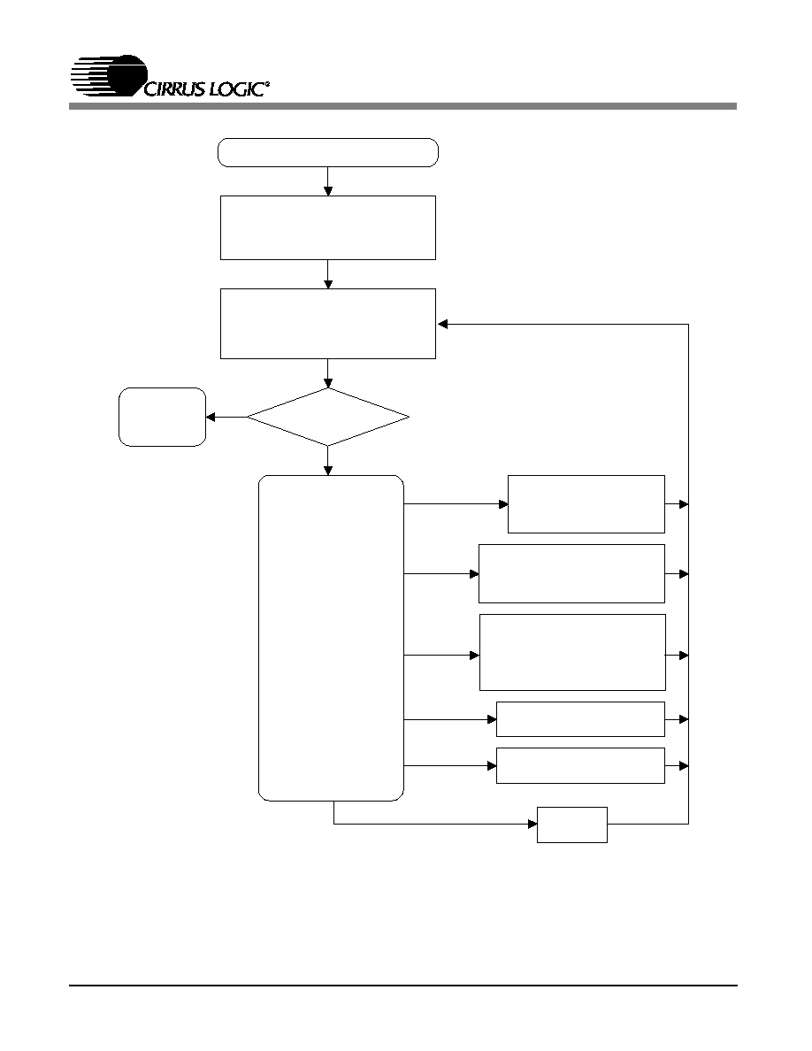
An enabled interrupt occurs.
The selected interrupt
request pin is driven high
(active) if not already high.
ISQ = 0000h?
Yes
The host reads the ISQ.
The selected interrupt
request pin is driven low.
No
Process applicable
RxEvent bits: Extradata,
Runt, CRCerror, RxOK.
Process applicable
TxEvent bits: 16coll, Jabber,
Out-of-window, TxOK.
Process applicable BufEvent
bits: RxDest, Rx128, RxMiss,
TxUnderrun, Rdy4Tx,
RxDMAFrame, SWint.
Process RxMISS counter.
Process TxCOL counter.
Which
Event
report
type?
RxEvent
TxEvent
BufEvent
RxMISS
TxCOL
None of the above
Service
Default
EXIT.
Interrupts
re-enabled.
Figure 5.1. Interrupt Status Queue
CS8920A
DS238PP2
87
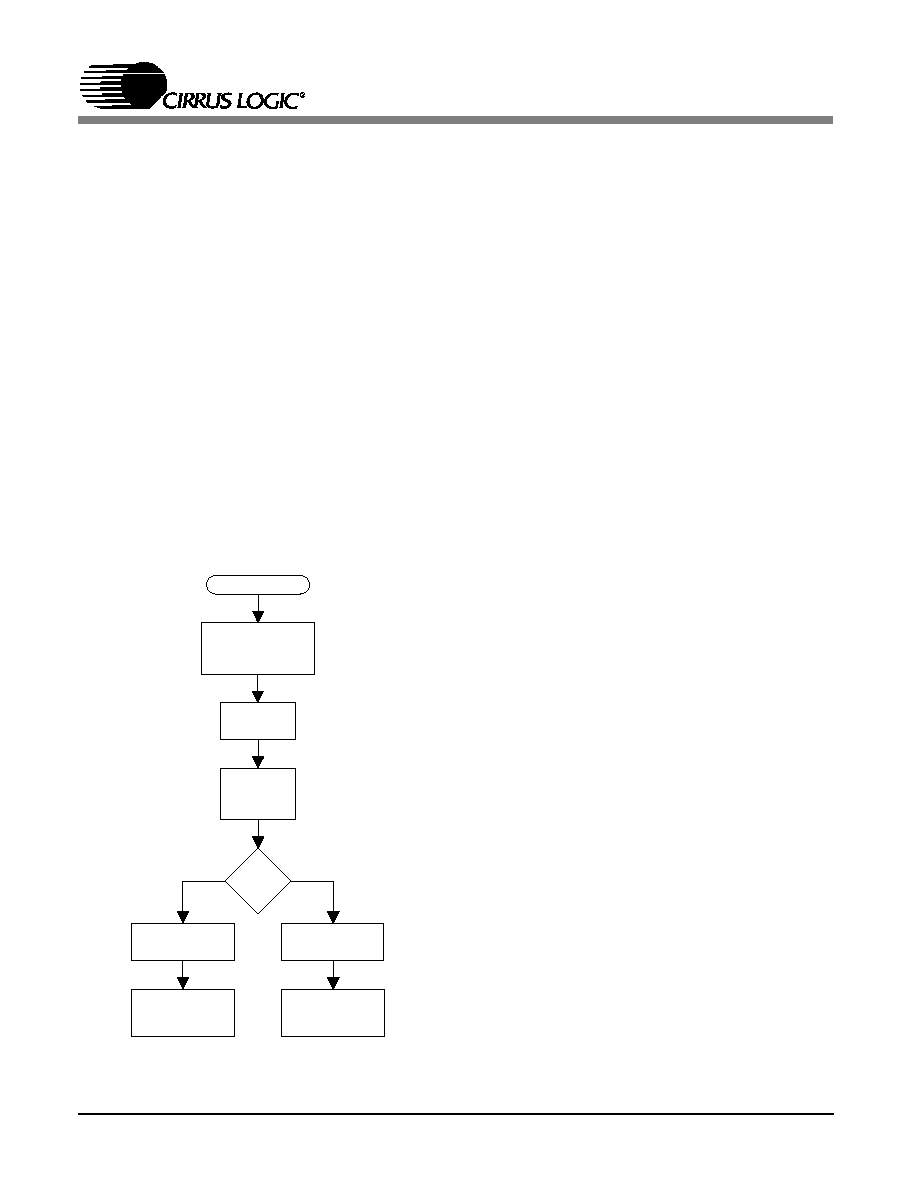
5.2
Basic Receive Operation
Overview
When an incoming packet has passed through
the analog front end and Manchester decoder, it
goes through the following three-step receive
process:
1. Pre-Processing
2. Temporary Buffering
3. Transfer to Host
Figure 5.2 shows the steps in frame reception.
As shown in the figure, all receive frames go
through the same pre-processing and temporary
buffering phases, regardless of transfer method.
When a frame has been pre-processed and buff-
ered, it can be accessed by the host in either
Memory or I/O space. In addition, the CS8920A
can transfer receive frames to host memory via
host DMA. This section describes receive frame
pre-processing and Memory and I/O space re-
ceive operation. Sections 5 . 5 t hrou gh 5.6
describe DMA operation.
5.2.1
Terminology: Packet, Frame, and
Transfer
The terms Packet, Frame, and Transfer are used
extensively in the following sections. They are
defined below for clarity.
Packet: The term "packet" refers to the entire se-
rial string of bits transmitted over an Ethernet
network. This includes the preamble, Start-of-
Frame Delimiter (SFD), Destination Address
(DA), Source Address (SA), Length field, Data
field, pad bits (if necessary), and Frame Check
Sequence (FCS, also called CRC). Figure 3.6
shows the format of a packet.
Frame: The term "frame" refers to the portion of
a packet from the DA to the FCS. This includes
the Destination Address (DA), Source Address
(SA), Length field, Data field, pad bits (if neces-
sary), and Frame Check Sequence (FCS, also
called CRC). Figure 3.6 shows the format of a
frame. The term "frame data" refers to all the
data from the DA to the FCS that is to be trans-
mitted, or that has been received.
Transfer: The term "transfer" refers to moving
data across the ISA bus, to and from the
CS8920A. During receive operations, only frame
data are transferred from the CS8920A to the
host (the preamble and SFD are stripped off by
the CS8920A's MAC engine). The FCS may or
may not be transferred, depending on the con-
figuration. All transfers to and from the
CS8920A are counted in bytes, but may be pad-
ded for word alignment.
Yes
No
Use
DMA?
Frame Held
On Chip
Frame DMAed
to Host Memory
Host Reads
Frame from
Host Memory
Frame Pre-
Processed
Frame
Temporarily
Buffered
Packet Received
Preamble and
Start-of-Frame
Delimiter Removed
Host Reads
Frame from
CS8920A Memory
Figure 5.2. Frame Reception
CS8920A
88
DS238PP2
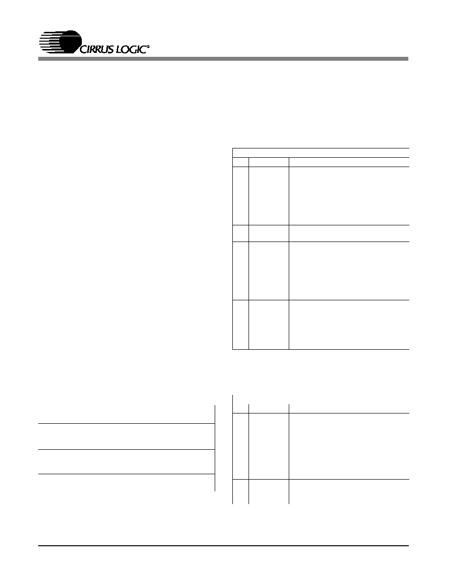
5.2.2
Receive Configuration
After each reset, the CS8920A must be config-
ured for receive operation. This can be done
automatically using an attached EEPROM, or by
wr it i ng c o nfi g ur at i on c o mman d s t o th e
CS8920A's internal registers (see Section 3.3).
The items that must be configured include:
∑
which physical interface to use;
∑
which types of frames to accept;
∑
which receive events cause interrupts; and,
∑
how received frames are transferred.
Configuring the Physical Interface: Configuring
the physical interface consists of determining
which Ethernet interface should be active and
enabling the receive logic for serial reception.
This is done via the LineCTL register (Register
13) and is described in Table 5.1.
Choosing Which Frame Types to Accept: The
RxCTL register (Register 5) is used to determine
which frame types will be accepted by the
CS8920A (a receive frame is said to be "ac-
cepted" when the frame is buffered, either on
chip or in host memory via DMA). Table 5.2 de-
scribes the configuration bits in this register.
Refer to Section 5.3 for a detailed description of
Destination Address filtering.
Selecting Which Events Cause Interrupts: The
RxCFG register (Register 3) and the BufCFG
register (Register B) are used to determine which
receive events will cause interrupts to the host
processor. Table 5.3 describes the interrupt en-
able (iE) bits in these registers.
Register 13, LineCTL
Bit
Bit Name
Operation
6
SerRxON
When set, reception enabled.
8
AUIonly
W h e n s e t , AU I s e l e c t e d ( ta ke s
precedence over AutoAUI/10BT).
9
AutoAUI/
10BT
When set, automatic interface selection
enabled. When both bits 8 and 9 are
clear, 10BASE-T selected.
E
LoRx
Squelch
W he n s et , r eceiver squelc h level
reduced by approximately 6 dB.
Table 5.1. Physical Interface Configuration
Register 5, RxCTL
Bit
Bit Name
Operation
6
IAHashA
When set, Individual Address frames
that pass the hash filter are accepted*.
7
Promis
cuousA
When set, all frames are accepted*.
8
RxOKA
When set, frames with valid length and
CRC and that pass the DA filter are
accepted.
9
MulticastA
When set, Multicast frames that pass
the hash filter accepted*.
A
IndividualA When set, frames with DA that matches
the IA at PacketPage base + 0158h are
accepted*.
B
BroadcastA When set, all broadcast frames are
accepted*.
C
CRCerrorA When set, frames with bad CRC that
pass the DA filter are accepted.
D
RuntA
when set, frames shorter than 64 bytes
that pass the DA filter are accepted.
E
ExtradataA When set, frames longer than 1518
byt es that pass the DA fil ter are
accepted (only the first 1518 bytes are
buffered).
* Must also meet the criteria programmed into
bits 8, C, D, and E.
Table 5.2. Frame Acceptance Criteria
Register 3, RxCFG
Bit
Bit Name
Operation
8
RxOKiE
When set, there is an interrupt if a
frame is received with valid length and
CRC*.
C
CRCerroriE When set, there is an interrupt if a
frame is received with bad CRC*.
D
RuntiE
When set, there is an interrupt if a
frame is received that is shorter than
64 bytes*.
E
ExtradataiE When set, there is an interrupt if a
frame is received that is longer than
1518 bytes*.
* Must also pass the DA filter before there is an
interrupt.
CS8920A
DS238PP2
89

Choosing How to Transfer Frames: The RxCFG
register (Register 3) and the BusCTL register
(Register 17) are used to determine how frames
will be transferred to host memory, as described
in Table 5.4.
5.2.3
Receive Frame Pre-Processing
The CS8920A pre-processes all receive frames
using a four step process:
1. Destination Address filtering;
2. Early Interrupt Generation;
3. Acceptance filtering; and,
4. Normal Interrupt Generation.
Figure 5.3 provides a diagram of frame pre-
processing.
Destination Address Filtering: All incoming
frames are passed through the Destination Ad-
dress filter (DA filter). If the frame's DA passes
the DA filter, the frame is passed on for further
pre-processing. If it fails the DA filter, the frame
is discarded. See Section 5.3 for a more detailed
description of DA filtering.
Early Interrupt Generation: The CS8920A sup-
ports the following two early interrupts that can
be used to inform the host that a frame is being
received:
∑
R xD est : T h e R xDest bit (Registe r C,
BufEvent, Bit F) is set as soon as the Desti-
nation Address (DA) of the incoming frame
passes the DA filter. When the RxDestiE bit
(Register B, BufCFG, bit F) is set, the
CS8920A generates a corresponding inter-
rupt. When RxDest is set, the host is
allowed to read the incoming frame's DA
(the first 6 bytes of the frame).
∑
R x1 2 8: T h e R x1 28 b it (R egi st er C,
BufEvent, Bit B) is set as soon as the first
128 bytes of the incoming frame have been
received. When the Rx128iE bit (Register B,
BufCFG, bit B) is set, the CS8920A gener-
ates a corresponding interrupt. When the
Rx128 bit is set, the RxDest bit is cleared
and the host is allowed to read the first 128
bytes of the incoming frame. The Rx128 bit
is cleared by the host reading the BufEvent
register (either directly or through the Inter-
rupt Status Queue) or by the CS8920A
Register B, BufCFG
Bit
Bit Name
Operation
7
RxDMAiE
When set, there is an interrupt if one or
more frames are transferred via DMA.
A
RxMissiE
When set, there is an interrupt if a
frame is missed due to insufficient
receive buffer space.
B
Rx128iE
When set, there is an interrupt after the
first 128 bytes of receive data have
been buffered.
D
MissOvfloiE When set, there is an interrupt if the
RxMISS counter overflows.
F
RxDestiE
When set, there is an interrupt after the
DA of an incoming frame has been
buffered.
Table 5.3. Registers 3 & B
Interrupt Configuration
Register 3, RxCFG
Bit
Bit Name
Operation
7
StreamE
When set, StreamTransfer enabled.
9
RxDMAonly When set, DMA slave operation used
for all receive frames.
A
AutoRx
DMAE
When set, Auto-Switch DMA enabled.
Register 17, BusCTL
Bit
Bit Name
Operation
B
DMABurst
When set, DMA operations hold the
bus for up to approximately 28
µ
s.
W he n c l ear, DM A operations are
continuous.
F
RxDMAsize W hen set, DMA buffer size is 64
Kbytes. When clear, DMA buffer size is
16 Kbytes.
Table 5.4. Frame Transfer Method
CS8920A
90
DS238PP2

detecting the incoming frame's End-of-Frame
(EOF) sequence.
Like all Event bits, RxDest and Rx128 are set by
the CS8920A whenever the appropriate event oc-
curs. Unlike other Event bits, RxDest and Rx128
may be cleared by the CS8920A without host in-
tervention. All other event bits are cleared only
by the host reading the appropriate event register,
either directly or through the Interrupt Status
Queue (ISQ). (RxDest and Rx128 can also be
cleared by the host reading the BufEvent register,
either directly or through the Interrupt Status
Queue). Figure 5.4 provides a diagram of the
Early Interrupt process.
Acceptance Filtering: The third step of pre-proc-
essing is to determine whether or not to accept
the frame by comparing the frame with the crite-
ria programmed into the RxCTL register
(Register 5). When the receive frame passes the
Acceptance filter, the frame is buffered, either on
chip or in host memory via DMA. If the frame
fails the Acceptance filter, it is discarded. The re-
sults of the Acceptance filter are reported in the
RxEvent register (Register 4).
Normal Interrupt Generation: The final step of
pre-processing is to generate any enabled inter-
rupts that are triggered by the incoming frame.
Interrupt generation occurs when the entire frame
has been buffered (up to the first 1518 bytes).
For more information about interrupt generation,
see Section 5.1.
5.2.4
Held vs. DMAed Receive Frames
All accepted frames are either held in on-chip
RAM until processed by the host, or stored in
host memory via DMA. A receive frame that is
held in on-chip RAM is referred to as a held re-
ceive frame. A frame that is stored in host
memory via DMA is a DMAed receive frame.
This section describes buffering and transferring
held receive frames. Sections 5.5 through 5.7 de-
scribe DMAed receive frames.
Pass
DA Filter?
Discard Frame
Destination
Address Filter
Check:
- PromiscuousA?
- IAHashA?
- MulticastA?
- IndividualA?
- BroadcastA?
Receive Frame
Yes
No
Yes
No
Generate Interrupts
Check:
- RxOKiE?
- ExtradataiE?
- CRCerroriE?
- RuntiE?
- RxDMAiE?
Pre-Processing
Complete
Generate Early
Interrupts if Enabled
(see figure 5.3)
Acceptance Filter
Check:
- RxOKA?
- ExtradataA?
- RuntA?
- CRCerrorA?
Status of receive
frame reported in
RxEvent register,
frame discarded.
Status of receive
frame reported in
RxEvent register,
frame accepted
into on-chip RAM
Pass
Accept.
Filter?
Figure 5.3. Receive Frame Pre-Processing
CS8920A
DS238PP2
91
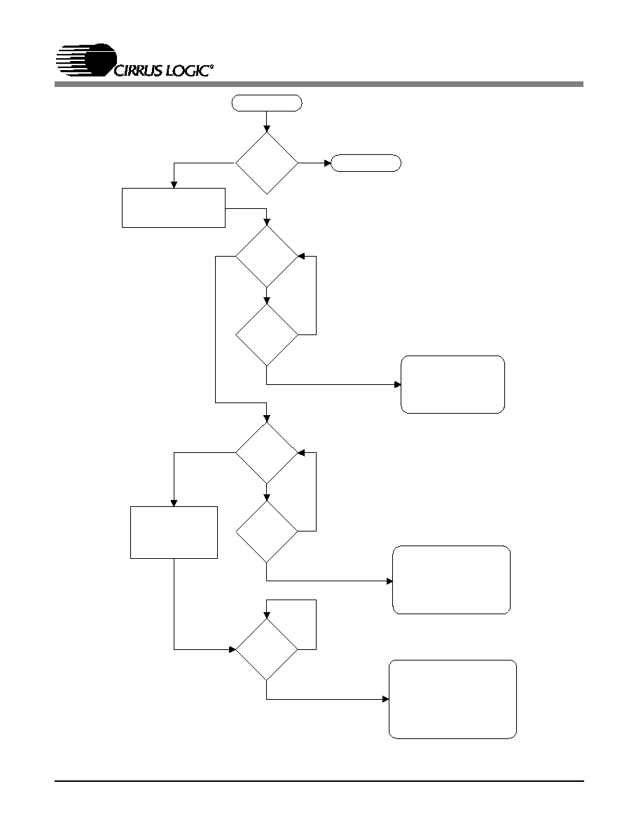
EOF
Received?
128 bytes
Received?
EOF
Received?
64 bytes
Received?
EOF
Received?
Receive Frame
RxDest cleared
and Runt set.
If RuntA is set,
frame accepted and
Host may read frame.
RxDest cleared and
RxOK or CRCerror
set, as appropriate.
If RxOKA or CRCerrorA
is set, frame accepted and
Host may read frame.
Rx128 cleared and
RxOK, CRCerror or
Extradata set, as
appropriate. If ExtradataA,
RxOKA or CRCerrorA is
set, frame is accepted and
Host may read frame.
DA Filter
Passed?
Yes
No
Yes
No
No
Yes
Yes
No
No
Yes
Rx128 set and
RxDest cleared.
Host may read first
128 received bytes.
Yes
No
Discard Frame
RxDest set.
Host may read the DA
(first 6 received bytes).
Figure 5.4. Early Interrupt Generation
CS8920A
92
DS238PP2

5.2.5
Buffering Held Receive Frames
If space is available, an incoming frame will be
temporarily stored in on-chip RAM, where it
awaits processing by the host. Although this re-
ceive frame now occupies on-chip memory, the
CS8920A does not commit the memory space to
it until one of the following two conditions is
true:
1. The entire frame has been received and the
host has learned about the frame by reading
the RxEvent register (Register 4), either di-
rectly or through the ISQ.
Or:
2. The frame has been partially received, causing
either the RxDest bit (Register C, BufEvent,
Bi t F) or t he Rx1 28 bit (Registe r C,
BufEvent, Bit B) to become set, and the host
has learned about the receive frame by read-
ing the BufEvent register (Register C), either
directly or through the ISQ.
When the CS8920A commits buffer space to a
particular held receive frame (termed a commit-
ted received frame), no data from subsequent
frames can be written to that buffer space until
the frame is freed from commitment. (The com-
mitted received frame may or may not have been
received error free.)
A received frame is freed from commitment by
either of the following conditions:
1. The host reads the entire frame sequentially in
the order that it was received (first byte in,
first byte out).
Or:
2. The host reads part or none of the frame, and
then issues a Skip command by setting the
Skip_1 bit (Register 3, RxCFG, bit 6).
Both early interrupts are disabled whenever there
is a committed receive frame waiting to be proc-
essed by the host.
5.2.6
Transferring Held Receive Frames
The host can read out held receive frames in
Memory or I/O space. To transfer frames in
Memory space, the host executes repetitive Move
instructions (REP MOVS) from PacketPage base
+ 0404h. To transfer frames in I/O space, the
host executes repetitive In instructions (REP IN)
from I/O base + 0000h, with status and length
preceding the frame.
There are three possible ways that the host can
learn the status of a particular frame. It can:
1. Read the Interrupt Status Queue;
2. Read the RxEvent register directly (Register 4);
or
3. Read the RxStatus register (PacketPage base +
0400h).
5.2.7
Receive Frame Visibility
Only one receive frame is visible to the host at a
time. The receive frame's status can be read from
the RxStatus register (PacketPage base + 0400h)
and its length can be read from the RxLength
register (PacketPage base + 0402h). For more in-
formation about Memory space operation, see
Section 4.11. For more information about I/O
space operation, see Section 4.12.
5.2.8
Example of Memory Mode Receive
Operation
A common length for short frames is 64 bytes,
including the 4-byte CRC. Suppose that such a
frame has been received with the CS8920A con-
figured as follows:
CS8920A
DS238PP2
93

∑
The BufferCRC bit (Register 3, RxCFG, Bit
B) is set causing the 4-byte CRC to be buff-
ered with the rest of the receive data.
∑
The RxOKA bit (Register 5, RxCTL, Bit 8)
is set, causing the CS8920A to accept good
frames (a good frame is one with legal length
and valid CRC).
∑
The RxOKiE bit (Register 3, RxCFG, Bit 8)
is set, causing an interrupt to be generated
whenever a good frame is received.
Then the transfer to the host would proceed as
follows:
1. The CS8920A generates an RxOK interrupt to
the host to signal the arrival of a good frame.
2. The host reads the ISQ (PacketPage base +
0120h) to assess the status of the receive
frame and sees the contents of the RxEvent
register (Register 4) with the RxOK bit (Bit 8)
set.
3. The host reads the receive frame's length from
the RxLength register (PacketPage base +
0402h).
4. The host reads the frame data by executing 32
consecutive MOV instructions from Packet-
Page base + 0404h.
The memory map of the 64-byte frame is given
in Table 5.5.
5.2.9
Receive Frame Byte Counter
The receive frame byte counter describes the
number of bytes received for the current frame.
The counter is incremented in real time as bytes
are received from the Ethernet. The byte counter
can be used by the driver to determine how many
bytes are available for reading out of the
CS8920A. Maximum Ethernet throughput can be
achieved by using I/O or memory modes, and by
dedicating the CPU to reading this counter, and
using the count to read the frame out of the
CS8920A at the same time it is being received
by the CS8920A from the Ethernet (parallel
frame-reception and frame-read-out tasks).
The byte count register resides at PacketPage
base + 50h.
Following an RxDest or Rx128 interrupt, the
register contains the number of bytes which are
available to be read by the CPU. When the end
of frame is reached, the count contains the final
count value for the frame, including the allow-
ance for the BufferCRC option. When this final
count is read by the CPU, the count register is
set to zero. Therefore, to read a complete frame
using the byte count register, the register can be
read and the data moved until a count of zero is
detected. The RxEvent register can then be read
to determine the final frame status.
The sequence is as follows:
1. At the start of a frame, the byte counter
matches the incoming character counter.
2. At the end of the frame, the final count includ-
ing the allowance for the CRC (if the
Memory Space
Word Offset
Description of Data Stored in On-
chip RAM
0400h
RxStatus Register (the host may
skip reading 0400h since
RxEvent was read from the ISQ.)
0402h
RxLength Register (In this
example, the length is 40h bytes.
The frame starts at 0404h, and
runs through 0443h.)
0404h to 0409h
6-byte Destination Address.
040Ah to 040Fh
6-byte Source Address.
0410h to 011h
2-byte Length or Type Field.
0412h to 043Fh
46 bytes of data.
0440h
CRC, bytes 1 and 2
0442h
CRC, bytes 3 and 4
Table 5.5. Example Memory Map
CS8920A
94
DS238PP2

BufferCRC option is enabled), is held until
the byte counter is read.
3. When a read of the byte counter returns a
count of zero, the previous count was the final
count.
4. RxEvent should be read to obtain a final status
of the frame, followed by a Skip command to
complete the operation.
Note that all RxEvent's should be processed be-
fore using the byte counter. The byte counter
should be used following a BufEvent when
RxDest or Rx128 interrupts are enabled.
5.3
Receive Frame Address Filtering
The CS8920A is equipped with a Destination
Address (DA) filter used to determine which re-
ceive frames will be accepted. (A receive frame
is said to be "accepted" by the CS8920A when
the frame data are placed in either on-chip mem-
ory, or in host memory by DMA). The DA filter
can be configured to accept the following frame
types:
Individual Address Frames: For all Individual
Address frames, the first bit of the DA is a 0
(DA[0] = 0), indicating that the address is a
Physical Address. The address filter accepts Indi-
vidual Address frames whose DA matches the
Individual Address (IA) stored at PacketPage
base + 0158h, or whose hash-filtered DA
matches one of the bits programmed into the
Logical Address Filter (the hash filter is de-
scribed later in this section).
Multicast Frames: For Multicast Frames, the
first bit of the DA is a 1 (DA[0] = 1), indicating
that the frame is a Logical Address. The address
filter accepts Multicast frames whose hash-fil-
tered DA matches one of the bits programmed
into the Logical Address Filter (the hash filter is
described later is this section). As shown in Table
5.7, Broadcast Frames can be accepted as Multi-
cast frames under a very specific set of condi-
tions.
Broadcast Frames: Broadcast frames have a
DA equal to FFFF FFFF FFFFh.
In addition, the CS8920A can be configured for
Promiscuous Mode, in which case it will accept
all receive frames, irrespective of DA.
Configuring the Destination Address Filter
The DA filter is configured by programming five
DA filter bits in the RxCTL register (Register 5):
IAHashA, PromiscuousA, MulticastA, Individu-
alA, and BroadcastA. Four of these bits are
associated with four status bits in the RxEvent
register (Register 4): IAHash, Hashed, Individu-
alAdr, and Broadcast. The RxEvent register
reports the results of the DA filter for a given
receive frame. The bits associated with DA filter-
ing are summarized below:
Bit #
RxCTL
Register 5
RxEvent
Register 4
6
IAHashA
IAHash
(used only if IAHashA = 1)
7
PromiscuousA
9
MulticastA
Hashed
A
IndividualA
IndividualAdr
(used only if IndividualA = 1)
B
BroadcastA
Broadcast
(used only if BroadcastA = 1)
The IAHashA, MulticastA, IndividualA, and
BroadcastA bits are used independently. As a re-
sult, many DA filter combinations are possible.
For example, if MulticastA and IndividualA are
set, then all frames that are either Multicast or
Individual Address frames are accepted. The
PromiscuousA bit, when set, overrides the other
four DA bits and allows all valid frames to be
accepted. Table 5.6 summarizes the configuration
options available for DA filtering.
CS8920A
DS238PP2
95

It may become necessary for the host to change
the Destination Address (DA) filter criteria with-
out resetting the CS8920A. This can be done as
follows:
1. Clear SerRxON (Register 13, LineCTL, Bit 6)
to prevent any additional receive frames while
the filter is being changed.
2. Modify the DA filter bits (B, A, 9, 7, and 6) in
the RxCTL register. Modify the Logical Ad-
dress Filter at PacketPage base + 0150h, if
necessary. Modify the Individual Address at
PacketPage base + 0158h, if necessary.
3. Set SerRxON to re-enable the receiver.
Because the receiver has been disabled, the
CS8920A will ignore frames while the host is
changing the DA filter.
Hash Filter
The hash filter is used to help determine which
Multicast frames and which Individual Address
frames should be accepted by the CS8920A.
Hash Filter Operation: See Figure 5.5. The DA
of the incoming frame is passed through the
CRC logic, generating a 32-bit CRC value. The
six most-significant bits of the CRC are latched
into the 6-bit hash register (HR). The contents of
the HR are passed through a 6-to-64-bit decoder,
asserting one of the decoder's outputs. The as-
serted output is compared with a corresponding
bit in the 64-bit Logical Address Filter, located at
PacketPage base + 0150h. If the decoder output
and the Logical Address Filter bit match, the
frame passes the hash filter and the Hashed bit
(Register 4, RxEvent, Bit 9) is set. If the two do
not match, the frame fails the filter and the
Hashed bit is clear.
Whenever the hash filter is passed by a "good"
frame, the RxOK bit (Register 4, RxEvent, Bit 8)
is set and the bits in the HR are mapped to the
Hash Table Index bits (Register 4, RxEvent, Bits
A through F).
Broadcast Frame Hashing Exception
Table 5.7 describes in detail the content of the
RxEvent register for each output of the hash and
address filters and describes an exception to nor-
mal processing. That exception can occur when
the hash-filter Broadcast address matches a bit in
the Logical Address Filter. To properly account
for this exception, the software driver should use
the following test to determine if the RxEvent
register contains a normal RxEvent (meaning bits
E-A are used for Extradata, Runt, CRC Error,
Broadcast and IndividualAdr) or a hash-table
RxEvent (meaning bits F-A contain the Hash Ta-
ble Index).
IAHashA
PromiscuousA
MulticastA
IndividualA
BroadcastA
Frames Accepted
0
0
0
1
0
Individual Address frames
with DA matching the IA at
PacketPage base + 0158h
1
0
0
0
0
Individual Address frames
with DA that pass the hash
filter (DA[0] must be 0)
0
0
1
0
0
Multicast frames with DA that
pass the hash filter (DA[0]
must be 1)
0
0
0
0
1
Broadcast frames
X
1
X
X
X
All frames
Table 5.6. Configuration Options for DA filtering
CS8920A
96
DS238PP2

64-bit Logical Address Filter (LAF)
Written into PacketPage base + 150h
6-to-64 decoder
1
64
CS8920A
CRC
Logic
Destination Address (DA)
from incoming frame
32-bit CRC value
(MSB)
(LSB)
6-bit Hash Register (HR)
[Hash Table Index]
64-input
OR gate
to
Hashed
bit
Figure 5.5. Hash Filter Operation
Address
Type of
Received
Frame
Erred
Frame?
Passes
Hash
Filter?
Contents of RxEvent
Bits F-A
Bit 9
Hashed
Bit 8
RxOK
Bit 6
IAHash
Individual
Address
no
yes
Hash Table Index
1
1
1
no
no
ExtraRuntCRCBroadcastIndividual
DataErrorAdr
0
1
0
yes
don't care
ExtraRuntCRCBroadcastIndividual
DataErrorAdr
0
0
0
Multicast
Address
no
yes
Hash table index
1
1
0
no
no
ExtraRuntCRCBroadcastIndividual
DataErrorAdr
0
1
0
yes
don't care
ExtraRuntCRCBroadcastIndividual
DataErrorAdr
0
0
0
Broadcast
Address
no
yes (Note 1)
ExtraRuntCRCBroadcastIndividual
DataErrorAdr
(actual value X00010)
1
1
0
no
no
ExtraRuntCRCBroadcastIndividual
DataErrorAdr
0
1
0
yes
don't care
ExtraRuntCRCBroadcastIndividual
DataErrorAdr
0
0
0
NOTES:
1. Broadcast frames are accepted as Multicast frames if and only if all the following conditions are
met simultaneously:
a) the Logical Address Filter is programmed as: (MSB) 0000 8000 0000 0000h (LSB). Note that
this LAF value corresponds to a Multicast Addresses of both all 1s and 03-00-00-00-00-01.
b) The Rx Control Register (register 5) is programmed to accept IndividualA, MulticastA, RxOK-only,
and the following address filters were enabled: IAHashA and BroadcastA.
2. NOT (Note 1).
3. This frame is accepted if the promiscuous accept bit is set.
4. This frame is accepted if either promiscuous accept or broadcast accept bit are set.
Table 5.7. Contents of RxEvent Upon Various Conditions
CS8920A
DS238PP2
97

If
bit Hashed =0, or
bit RxOK=0, or
(bits F-A = 02h and the destination
address is all ones)
then RxEvent contains a normal RxEvent
else RxEvent contained a hash RxEvent.
5.4
Rx Missed and Tx Collision Counters
5.4.1
RxMiss counter
The RxMiss counter is (Register 10) incremented
when receive data are lost (missed) due to slow
movement of the data out of the receive buffer.
RxMiss is a ten-bit counter (bit 6 to bit F) with
bit 6 as the LSB. RxMiss is cleared when read.
When MissOvfloiE is (Register B, Buf CFG, bit
D) set, there is an interrupt when RxMiss incre-
ments from 1FFh to 200h. The actual overflow is
at 3FFh. Interrupting at 200h provides an addi-
tional 512 (decimal) counts before RxMiss
actually overflows back to 000h.
5.4.2
TxCOL counter
The TxCol counter (Register 12) is incremented
when there is a transmit collision. TxCOL is a
ten-bit counter (bit 6 to bit F) with bit 6 as the
LSB. TxCOL is cleared when read.
When TxColOvfiE (Register B, Buf CFG, bit C)
is set, there is an interrupt when RxMiss incre-
ments from 1FFh to 200h. The actual overflow is
at 3FFh. Interrupting at 200h provides an addi-
tional 512 (decimal) counts before TxCOL
actually overflows back to 000h.
5.5
Receive DMA
5.5.1
Overview
The CS8920A supports a direct interface to the
host DMA controller allowing it to transfer re-
ceive frames to host memory via slave DMA.
The DMA option applies only to receive frames,
not to transmit operation. The CS8920A offers
three possible Receive DMA modes:
1. Receive-DMA-only mode: All receive frames
are transferred via DMA.
2. Auto-Switch DMA mode: DMA is used only
when needed to help prevent missed frames.
3. StreamTransfer mode: DMA is used to mini-
mize the number of interrupts to the host.
This section provides a description of Receive-
DM A-o n ly mod e. Sect ion 5.6 describes
Auto-Switch DMA and Section 5.7 describes
StreamTransfer.
5.5.2
Configuring the CS8920A for DMA
Operation
The CS8920A interfaces to the host DMA con-
t ro ll e r th ro u gh on e p ai r of the DMA
request/acknowledge pins (see Section 3.2 for a
description of the CS8920A's DMA interface).
Four registers are used for DMA operation.
These are described in Table 5.8.
Receive-DMA-only mode is enabled by setting
the RxDMAonly bit (Register 3, RxCFG, Bit 9).
Note that if the RxDMAonly bit and the
AutoRxDMAE bit (Register 3, RxCFG, Bit A)
are both set, then RxDMAonly takes precedence,
and the CS8920A is in DMA mode for all re-
ceive frames.
5.5.3
DMA Receive Buffer Size
In receive DMA mode, the CS8920A stores re-
ceived frames (along with their status and length)
in a circular buffer located in host memory
space. The size of the circular buffer is deter-
mined by the RxDMAsize bit (Register 17,
BusCTL, Bit D). When RxDMAsize is clear, the
CS8920A
98
DS238PP2

buffer size is 16 Kbytes. When RxDMAsize is
set, the buffer is 64 Kbytes. It is the host's task
to locate and keep track of the DMA receive
buffer's base address. The DMA Start-of-Frame
register is the only circuit affected by this bit.
APPLICATION NOTE: As a result of the PC ar-
chitecture, DMA cannot occur across a 128K
boundary in memory. Thus, the DMA buffer re-
served for the CS8920A must not cross a 128K
boundary in host memory if DMA operation is
desired. Requesting a 64K, rather than a 16K
buffer, increases the probability of crossing a
128K alignment boundary. After the driver re-
quests a DMA buffer, the driver must check for a
boundary crossing. If the boundary is crossed,
then the driver must disable DMA functionality.
5.5.4
Receive-DMA-Only Operation
If space is available, an incoming frame is tem-
porarily stored in on-chip RAM. When the entire
frame has been received, pre-processed, and ac-
cepted, the CS8920A signals the DMA controller
that a frame is to be transferred to host memory
by driving the selected DMA Request pin high.
The DMA controller acknowledges the request
by driving the DMA Acknowledge pin low. The
CS8920A then transfers the contents of the
RxStatus register (PacketPage base + 0400h) and
the RxLength register (PacketPage base + 0402h)
to host memory, followed by the frame data. If
the DMABurst bit (Register 17, BusCTL, Bit B)
is clear, the DMA Request pin remains high until
the entire frame is transferred. If the DMABurst
bit is set, the DMA Request pin (DMARQ) re-
mains high for approximately 28
µ
s then goes
low for approximately 1.3
µ
s to give the CPU
and other peripherals access to the bus.
The CS8920A's DMA request pin remains active
(HIGH), until all but one word is transferred.
The DMA request pin goes inactive just before
transfer of the last word. For an ISA bus, the
DMA request signal is latched during a DMA
cycle. Therefore, a DMA controller will gener-
ate one more cycle after the CS8920A's DMA
request pin goes inactive. The CS8920A expects
this additional DMA cycle after its DMA request
pin goes inactive.
When the transfer is complete, the CS8920A
does the following:
∑
updates the DMA Start-of-Frame register
(PacketPage base + 0026h);
∑
updates the DMA Frame Count register
(PacketPage base + 0028h);
∑
updates DMA Byte Count register (Packet-
Page base + 002Ah);
∑
sets the RxDMAFrame bit (Register C,
BufEvent, Bit 7); and,
∑
de-allocates the buffer space used by the
transferred frame.
In addition, if the RxDMAiE bit (Register B,
BufCFG, Bit 7) is set, a corresponding interrupt
occurs.
PacketPage
Address
Register Description
0374h
DMA Channel Number: DMA channel
number (0, 1, or 2) that defines the
DMARQ/DMACK pin pair used.
0026h
DMA Start-of-Frame: 16-bit value that
defines the offset from the DMA base
address to the start of the most recently
transferred received frame.
0028h
DMA Frame Count: The lower 12 bits
d e f i n e t h e n um b er of va l i d fr am e s
transferred via DMA since the last read-out
of this register. The upper 4 bits are
reserved and not applicable.
002Ah
DMA Byte Count: Defines the number of
bytes that have been transferred via DMA
since the last read-out of this register.
Table 5.8. Receive DMA Registers
CS8920A
DS238PP2
99

When the host processes DMAed frames, it must
read the DMA Frame Count register.
Whenever a receive frame is missed (lost) due to
insufficient receive buffer space, the RxMISS
counter (Register 10) is incremented. A missed
receive frame causes the counter to increment in
either DMA or non-DMA modes.
Note that when in DMA mode, reading the con-
tents of the RxEvent register will return 0000h.
Status information should be obtained from the
DMA buffer.
5.5.5
Committing Buffer Space to a DMAed
Frame
Although a receive frame may occupy space in
the host memory's circular DMA buffer, the
CS8920A's Memory Manager does not commit
the buffer space to the receive frame until the en-
tire frame has been transferred and the host
learns of the frame's existence by reading the
Frame Count register (PacketPage base + 0028h).
When the CS8920A commits DMA buffer space
to a particular DMAed receive frame (termed a
committed received frame), no data from sub-
sequent frames can be written to that buffer
space until the committed received frame is freed
from commitment. (The committed received
frame may or may not have been received error
free.)
A committed DMAed receive frame is freed
from commitment by any one of the following
conditions:
1. The host re-reads the DMA Frame Count regis-
ter (PacketPage base + 0028h).
2. New frames have been transferred via DMA,
and the host reads the BufEvent register
(either directly or from the ISQ) and sees that
the RxDMAFrame bit is set (Register C, bit
7) (this condition is termed an "implied
Skip").
3. The host issues a Reset-DMA command by
setting the ResetRxDMA bit (Register 17,
BusCTL, Bit 6).
5.5.6
DMA Buffer Organization
When DMA is used to transfer receive frames,
the DMA Start-of-Frame register (PacketPage
Base + 0026h) defines the offset from the DMA
base to the start of the most recently transferred
received frame. Frames stored in the DMA buff-
er are transferred as words and maintain
double-word (32-bit) alignment. Unfilled mem-
ory space between successive frames stored in
the DMA buffer may result from double-word
Non-StreamTransfer Mode
StreamTransfer Mode (see Section 5.7)
To Set RxDMAFrame
The RxDMAFrame bit is set whenever the DMA
Frame Count register (PacketPage base +
0028h) transitions to non-zero.
The RxDMAFrame bit is set at the end of a
StreamTransfer cycle.
To Clear RxDMAFrame The DMA Frame Count is zero.
The DMA Frame Count is zero.
Table 5.9. RxDMAFrame Bit
CS8920A
100
DS238PP2

alignment. These "holes" may be 1, 2, or 3 bytes,
depending on the length of the frame preceding
the hole.
5.5.7
RxDMAFrame Bit
The RxDMAFrame bit (Register C, BufEvent,
bit 7) is controlled by the CS8920A and is set
whenever the value in the DMA Frame Count
register is non-zero. The host cannot clear
RxDMAFrame by reading the BufEvent register
(Register C). Table 5.9 summarizes the criteria
used to set and clear RxDMAFrame.
5.5.8
Receive DMA Example Without
Wrap-Around
Figure 5.6 shows three frames stored in host
memory by DMA without wrap-around.
RxStatus - Frame 1
RxLength - Frame 1
RxStatus - Frame 2
RxLength - Frame 2
Frame 2
RxStatus - Frame 3
RxLength - Frame 3
Frame 3
DMA Buffer
Base Address
Frame 1
"Holes" due to
double-word
alignment
DMA Start-of-Frame
register (PacketPage
base + 0026H)
points here.
DMA Byte Count
(PacketPage base + 002Ah)
Figure 5.6. Example of Frames Stored in DMA Buffer
CS8920A
DS238PP2
101
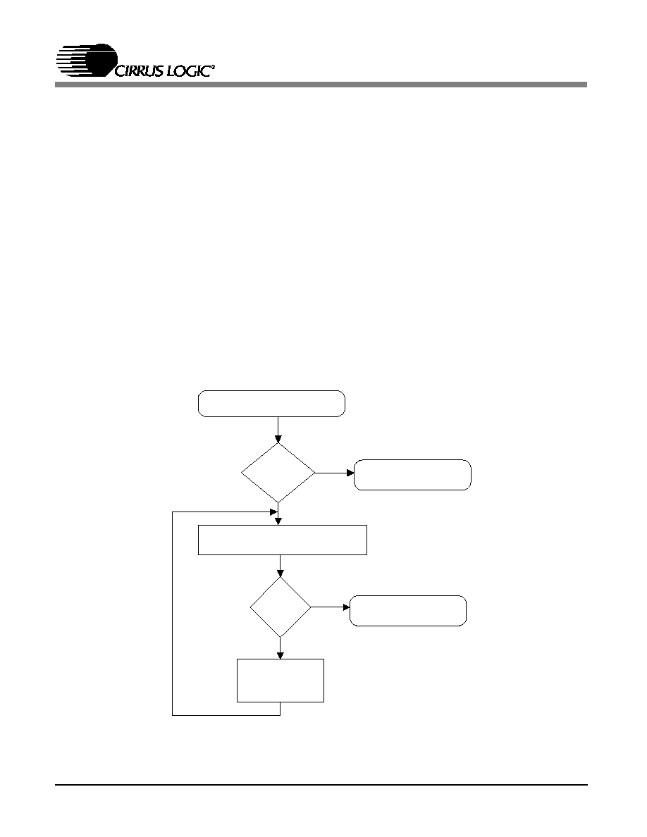
5.5.9
Receive DMA Operation for
RxDMA-Only Mode
In an RxDMAOnly mode, a system DMA moves
all the received frames from the on-chip memory
to an external 16- or 64-Kbyte buffer memory.
The received frame must have passed the desti-
nation address filter, and must be completely
received. Usually the DMA receive frame inter-
rupt (RxDMAiE, bit 7, Register B, BufCFG) is
set so that the CS8920A generates an interrupt
when a frame is transferred by DMA. Figure 5.7
shows how a DMA Receive Frame interrupt is
processed.
In the interrupt service routine, the BufEvent
register (register C), bit RxDMA Frame (bit 7)
indicates that one or more receive frames were
transferred using DMA. The software driver
should maintain a pointer (e.g. PDMA_START)
that will point to the beginning of a new frame.
After the CS8920A is initialized and before any
frame is received, pointer P
DMA_START
points to
the beginning of the DMA buffer memory area.
The first read of the DMA Frame Count, C
DMA
,
commits the memory covered by the C
DMA
count, and the DMA cannot overwrite this com-
mitted space until the space is freed. The driver
then processes the frames described by the
C
DMA
count and makes a second read of the
DMA frame count. This second read frees the
buffer memory space described by the C
DMA
counter.
During the frame processing, the software should
advance the P
DMA_START
pointer. At the end of
processing a frame, pointer P
DMA_START
should
Process the
C
DMA
Frames
Read the DMA frame Count (C
DMA
)
(PacketPage base + 0028h)
No
C
DMA
= 0 ?
Host Enters Interrupt Routine
Process other events
that caused interrupt
Yes
No
RxDMA
Frame
bit set?
Process other events
that caused interrupt
Yes
Figure 5.7. RxDMA Only Operation
CS8920A
102
DS238PP2
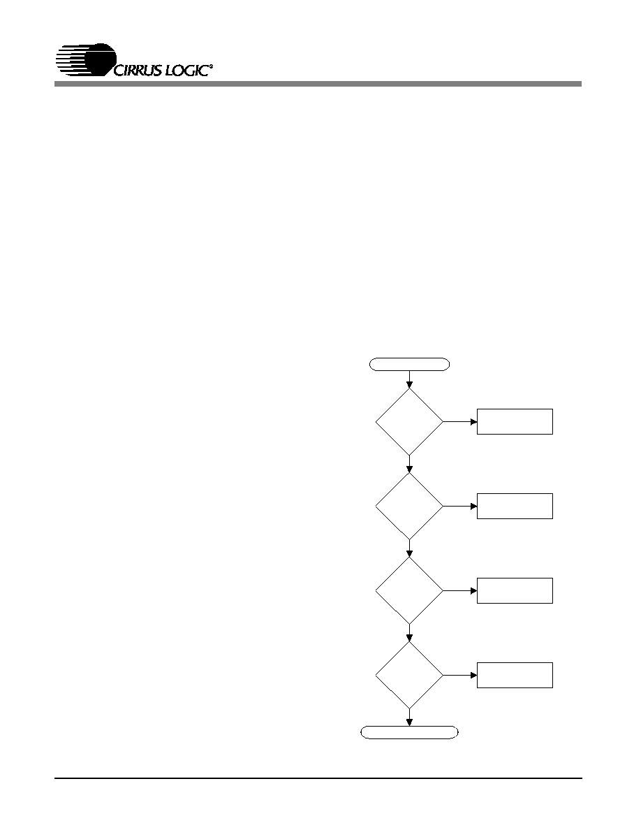
be made to align with a double-word boundary.
The software remains in the loop until the DMA
frame count read is zero.
5.6
Auto-Switch DMA
Overview
The CS8920A supports a unique feature, Auto-
Switch DMA, that allows it to switch between
Memory or I/O mode and Receive DMA auto-
ma ti c al l y. Au t o- Swi tch DMA a llows th e
CS8920A to realize the performance advantages
of Memory or I/O mode while minimizing the
number of missed frames that could result due to
slow processing by the host.
Configuring the CS8920A for Auto-Switch
DMA
Auto-Switch DMA mode requires the same con-
figuration as Receive-DMA-only mode, with one
exception: the AutoRxDMAE bit (Register 3,
R xC FG, Bi t A) mus t b e s et , and th e
RxDMAonly bit (Register 3, RxCFG, Bit 9)
must be clear (see Section 5.5.2). In Auto-Switch
DMA mode, the CS8920A operates in non-DMA
mode if possible, only switching to slave DMA
if necessary.
Note that if the AutoRxDMAE bit and the
RxDMAonly bit (Register 3, RxCFG, bit 9) are
both set, the CS8920A uses DMA for all receive
frames.
Auto-Switch DMA Operation
Whenever a frame begins to be received in Auto-
Switch DMA mode, the CS8920A checks to see
if there is enough on-chip buffer space to store a
maximum length frame. If there is, the incoming
frame is pre-processed and buffered as normal.
If there isn't, the CS8920A's MAC engine com-
pares the frame's Destination Address (DA) to
the criteria programmed into the DA filter. If the
incoming DA fails the DA filter, the frame is dis-
carded. If the DA passes the DA filter, the
CS8920A automatically switches to DMA mode
and starts transferring the frame(s) currently be-
ing held in the on-chip buffer into host memory.
This frees up buffer space for the incoming
frame.
Figure 5.8 shows the steps the CS8920A goes
through in determining when to automatically
switch to DMA.
Whenever the CS8920A automatically enters
DMA, at least one complete frame is already
stored in the on-chip buffer. Because frames are
transferred to the host in the same order as re-
ceived (first in, first out), the beginning of the
received frame that triggered the switch to DMA
All Frames
use DMA
Yes
Yes
No
No
Yes
No
No
Yes
Frame
Discarded
Frame Buffered
in On-chip RAM
Auto-Switch
DMA Disabled
Packet Received
Auto-Switch to DMA
Frame
Passed the
DA filter?
RxDMA only
Bit=1
More
Buffer Space
Available?
AutoRxDMA
Bit=1?
Figure 5.8. Conditions for Switching to DMA
CS8920A
DS238PP2
103

is not the first frame to be transferred. Instead,
the oldest non-committed frame in the on-chip
buffer is the first frame to use DMA. When
DMA begins, any pending RxEvent reports in
the Interrupt Status Queue are discarded because
the host cannot process those events until the
corresponding frames have been completely
DMAed.
Auto-Switch DMA works only on entire received
frames. The CS8920A does not use Auto-Switch
DMA to transfer partial frames. Also, when a
frame has been committed (see Section 5.2.5),
the CS8920A will not switch to DMA mode un-
til the committed frame has been transferred
completely or skipped.
After a complete frame has been moved to host
memory, the CS8920A updates the DMA Start-
of-Frame register (PacketPage base + 0026h), the
DMA Frame Count register (PacketPage base +
0028h), and the DMA Byte Count register, then
se ts th e R xD MAF rame bit (Registe r C,
BufEvent, bit 7). If RxDMAiE (Register B,
BufCFG, bit 7) is set, a corresponding interrupt
occurs.
DMA Channel Speed vs. Missed Frames
When the CS8920A starts DMA, the entire old-
est, non-committed frame must be placed in host
memory before on-chip buffer space will be
freed for the next incoming frame. If the oldest
frame is relatively large, and the next incoming
frame is also large, the incoming frame may be
missed, depending on the speed of the DMA
channel. If this happens, the CS8920A will in-
crement the RxMiss counter (Register 10) and
clear any event reports (RxEvent and BufEvent)
associated with the missed frame.
Exit From DMA
When the CS8920A has activated receive DMA,
it remains in DMA mode until all of the follow-
ing are true:
∑
The host processes all RxEvent and
BufEvent reports pending in the ISQ.
∑
The host reads a zero value from the DMA
Frame Count register (PacketPage base +
0028h).
∑
The CS8920A is not in the process of trans-
ferring a frame via DMA.
Auto-Switch DMA Example
Figure 5.9 shows how the CS8920A enters and
exits Auto-Switch DMA mode.
CS8920A
104
DS238PP2
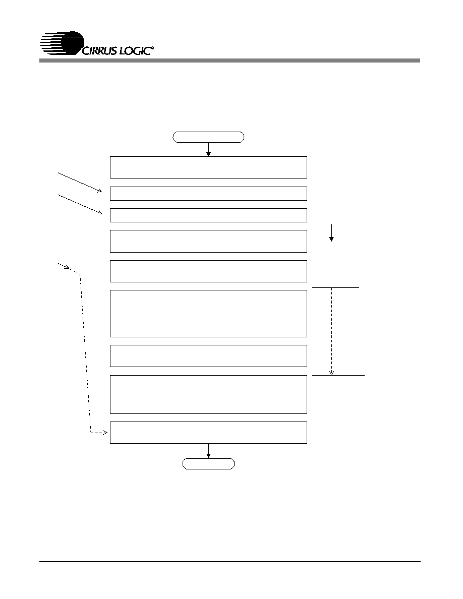
Fram
e 1
Fram
e 2
Frame 3 starts to be received and passes the DA filter.
This activates Auto-Switch DMA.
Fram
e 3
Frame 1 is placed in host memory via DMA freeing
space for the incoming Frame 3. The CS8920A updates
the DMA Frame Count, DMA Start of Frame and DMA
Byte Count registers. It then sets the RxDMA DMAFrame
bit and generates an interrupt.
Frame 2 is placed in host memory via DMA and the
CS8920A updates the DMA registers.
The host responds to the RxDMAFrame interrupt, and
reads the Frame Count register, which is cleared when
read. Since there are no receive interrupts pending, the
CS8920A exits DMA (assumes Frame 3 is still coming in).
Receive DMA used
during this time.
At this point, the CS8920A does not have sufficient buffer
space for another complete large frame (1518 bytes).
Frame 1 received and completely stored in on-chip RAM.
Frame 2 received and completely stored in on-chip RAM.
Enter Example Here
Exit Example
Time
Frame 3 is completely buffered in on-chip RAM, and
awaits processing by the host.
Entering this example, the receive buffer is empty and the
DMA Frame Count (PacketPage base + 0028h) is zero.
Figure 5.9. Example of Auto-Switch DMA
CS8920A
DS238PP2
105

5.7
StreamTransfer
Overview
The CS8920A supports an optional feature,
StreamTransfer, that can reduce the amount of
CPU overhead associated with frame reception.
StreamTransfer works during periods of high re-
ceive activity by grouping multiple receive
events into a single interrupt, thereby reducing
the number of receive interrupts to the host proc-
e ssor. Du ri ng p er io ds of pe ak lo adi ng,
StreamTransfer will eliminate 7 out of every 8
interrupts, cutting interrupt overhead by up to
87%.
Configuring the CS8920A for StreamTransfer
StreamTransfer is enabled by setting the StreamE
bit along with either the AutoRxDMAE bit or the
RxDMAonly bit in register Receiver Configura-
tion (register 3). (StreamTransfer must not be
selected unless either one of AutoRxDMAE or
RxDMA-only is selected.) StreamTransfer only
applies to "good" frames (frames of legal length
with valid CRC). Therefore, the RxOKA bit and
the RxOKiE bit must both be set. Finally,
StreamTransfer works on whole packets and is
not compatible with early interrupts. This re-
quires that the RxDestiE bit and the Rx128iE bit
both be clear.
Table 5.10 summarizes how to configure the
CS8920A for StreamTransfer.
StreamTransfer Operation
When StreamTransfer is enabled, the CS8920A
will initiate a StreamTransfer cycle whenever
two or more frames with the following charac-
teristics are received:
1. have passed the Destination Address filter;
2. are of legal length with valid CRC; and,
3. are spaced "back-to-back" (between 9.6 and 52
µ
s apart).
During a StreamTransfer cycle the CS8920A
does the following:
∑
delays the normal RxOK interrupt associated
with the first receive frame;
∑
switches to receive DMA mode;
∑
transfers up to eight receive frames into host
memory via DMA;
∑
updates the DMA Start-of-Frame register
(PacketPage base + 0026h);
∑
updates the DMA Frame Count register
(PacketPage base + 0028h);
∑
updates DMA Byte Count register (Packet-
Page base + 002Ah);
∑
sets the RxDMAFrame bit (Register C,
BufEvent, Bit 7); and,
∑
generates an RxDMAFrame interrupt.
Keeping StreamTransfer Mode Active
When the CS8920A initiates a StreamTransfer
cycle, it will continue to execute cycles as long
as the following conditions hold true:
Register Name
Bit
Bit Name
Value
Register 3, RxCFG
7
StreamE
1
8
RxOKiE
1
9
or
A
RxDMAonly
or
AutoRxDMA
1
or
1
Register 5, RxCTL
8
RxOKA
1
Register B, BufCFG
7
RxDMAiE
1
F
RxDestiE
0
B
Rx128iE
0
Table 5.10. Stream Transfer Configuration
CS8920A
106
DS238PP2

∑
all packets received are of legal length with
valid CRC;
∑
each packet follows its predecessor by less
than 52
µ
s; and,
∑
the DA of each packet passes the DA filter.
If any of these conditions are not met, the
CS8920A exits StreamTransfer by generating
RxOK and RxDMA interrupts. The CS8920A
then returns to either Memory, I/O, or DMA
mode, depending on configuration.
Example of StreamTransfer
Figure 5.10 shows how four back-to-back
frames, followed by five back-to-back frames,
would be received without StreamTransfer. Fig-
ure 5.11 shows how the same sequence of frames
would be received with StreamTransfer.
Receive DMA Summary
Table 5.11 summarizes the Receive DMA con-
figuration options supported by the CS8920A.
RxDMAonly
(Register 3,
RxCFG, Bit 9)
AutoRxDMAiE
(Register 3,
RxCFG, Bit A)
RxDMAiE
(Register B,
BufCFG, Bit 7)
RxOKiE
(Register 3,
RxCFG, Bit 8)
CS8920A Configuration
1
NA
0
0
Receive DMA used for all receive frames,
without interrupts.
1
NA
1
0
Receive DMA used for all receive frames, with
BufEvent interrupts.
0
1
0
0
Auto-Switch DMA used if necessary, without
interrupts.
0
1
1
1
Auto-Switch DMA used if necessary, with
RxEvent and BufEvent interrupts possible.
0
0
NA
1
Memory or I/O Mode only.
Table 5.11. Receive DMA Configuration Options
4 Back-to-Back Frames
5 Back-to-Back Frames
Interrupt
Request
9 Interrupts for 9 "Good" Packets
Time
T > 52 us
Figure 5.10. Receive Example Without Stream Transfer
4 Back-to-Back Frames
5 Back-to-Back Frames
Interrupt
Request
2 Interrupts for 9 "Good" Packets
Time
T > 52 us
Figure 5.11. Receive Example With Stream Transfer
CS8920A
DS238PP2
107

5.8
Transmit Operation
5.8.1
Overview
Packet transmission occurs in two phases. In the
first phase, the host moves the Ethernet frame
into the CS8920A's buffer memory. The first
phase begins with the host issuing a Transmit
Command. This informs the CS8920A that a
frame is to be transmitted and tells the chip when
(i.e. after 5, 381, or 1021 bytes have been trans-
ferred or after the full frame has been transferred
to the CS8920A) and how the frame should be
sent (i.e. with or without CRC, with or without
pad bits, etc.). The host follows the Transmit
Command with the Transmit Length, indicating
how much buffer space is required. When buffer
space is available, the host writes the Ethernet
frame into the CS8920A's internal memory, us-
ing either Memory or I/O space.
In the second phase of transmission, the
CS8920A converts the frame into an Ethernet
packet then transmits it onto the network. The
second phase begins with the CS8920A transmit-
ting the preamble and Start-of-Frame delimiter as
soon as the proper number of bytes have been
transferred into its transmit buffer (5, 381, 1021
bytes or full frame, depending on configuration).
The preamble and Start-of-Frame delimiter are
followed by the data transferred into the on-chip
buffer by the host (Destination Address, Source
Address, Length field and LLC data). If the
frame is less than 64 bytes, including CRC, the
CS8920A adds pad bits if configured to do so.
Finally, the CS8920A appends the proper 32-bit
CRC value.
5.8.2
Transmit Configuration
After each reset, the CS8920A must be config-
ured for transmit operation. This can be done
automatically, using an attached EEPROM, or by
wr it i ng c o nfi g ur at i on c o mman d s t o th e
CS8920A's internal registers (see Section 3.3).
The items that must be configured include which
physical interface to use and which transmit
events cause interrupts.
Configuring the Physical Interface: Configuring
the physical interface consists of determining
which Ethernet interface should be active
(10BASE-T or AUI), and enabling the transmit
logic for serial transmission. Configuring the
Physical Interface is accomplished via the
LineCTL register (Register 13) and is described
in Table 5.12.
No t e th a t th e C S8 92 0 A w ill tra nsmi t i n
10BASE-T mode when no link pulses are being
received only if bit DisableLT is set in register
Test Control (Register 19, bit 7).
Selecting which Events Cause Interrupts: The
TxCFG register (Register 7) and the BufCFG
register (Register B) are used to determine which
transmit events will cause interrupts to the host
processor. Tables 5.13 and 5.14 describe the in-
terrupt enable (iE) bits in these registers.
Register 13, LineCTL
Bit
Bit Name
Operation
7
SerTxON
When set, transmission enabled.
8
AUIonly
W h e n s e t , AU I s e l e c t e d ( ta ke s
precedence over AutoAUI/10BT). When
clear, 10BASE-T is selected.
9
AutoAUI/
10BT
When set, automatic interface
selection is enabled.
B
Mod
BackoffE
W h e n s et , t h e m od i f i ed b a ckof f
algorithm is used. When clear, the
standard backoff algorithm is used.
D
2-part
DefDis
When set, two-part deferral is disabled.
Table 5.12. Physical Interface Configuration
CS8920A
108
DS238PP2

5.8.3
Changing the Configuration
When the host configures these registers it does
not need to change them for subsequent packet
transmissions. If the host does choose to change
the TxCFG or BufCFG registers, it may do so at
any time. The effects of the change are noticed
immediately. That is, any changes in the Inter-
rupt Enable (iE) bits may affect the packet
currently being transmitted.
If the host chooses to change bits in the
LineCTL register after initialization, the Mod-
BackoffE bit and any receive related bit
(LoRxSquelch, SerRxON) may be changed at
any time. However, the AutoAUI/10BT and
AUIonly bits should not be changed while the
SerTxON bit is set. If any of these three bits are
to be changed, the host should first clear the
SerTxON bit (Register 13, LineCTL, Bit 7), and
then set it when the changes are complete.
5.8.4
Enabling CRC Generation and Padding
Whenever the host issues a Transmit Request
command, it must indicate whether or not the
Cyclic Redundancy Check (CRC) value should
be appended to the transmit frame, and whether
or not pad bits should be added (if needed). Ta-
ble 5.15 descri bes h ow to con fi gure the
CS8920A for CRC generating and padding.
5.8.5
Individual Packet Transmission
Whenever the host has a packet to transmit, it
must issue a Transmit Request to the CS8920A
consisting of the following three operations in
the exact order shown:
1. The host must write a Transmit Command to
the TxCMD register (PacketPage base +
0144h or I/O base +0004h). The contents of
Register 7, TxCFG
Bit
Bit Name
Operation
6
Loss-of-
CRSiE
W h e n s e t , t he r e i s a n i nt e rr up t
whenever the CS8920A fails to detect
Carrier Sense after transmitting the
preamble (applies to the AUI only).
7
SQEerroriE W h e n s e t , t he r e i s a n i nt e rr up t
whenever there is an SQE error.
8
TxOKiE
W h e n s e t , t he r e i s a n i nt e rr up t
w h e neve r a fr am e i s t ra ns mi tt ed
successfully.
9
Out-of-
windowiE
W h e n s e t , t he r e i s a n i nt e rr up t
whenever a late collision is detected.
A
JabberiE
W h e n s e t , t he r e i s a n i nt e rr up t
whenever there is a jabber condition.
B
AnycolliE
W h e n s e t , t he r e i s a n i nt e rr up t
whenever there is a collision.
F
16colliE
W h e n s e t , t he r e i s a n i nt e rr up t
whenever the CS8920A attempts to
transmit a single frame 16 times.
Table 5.13. Transmitting Interrupt Configuration
Register B, BufCFG
Bit
Bit Name
Operation
8
Rdy4TxiE
W h e n s e t , t he r e i s a n i nt e rr up t
w h e n eve r bu f fe r s p a c e b e c om e s
available for a transmit frame (used
with a Transmit Request).
9
TxUnder
RuniE
When set, there is an interrupt when
the CS8920A runs out of data after
transmit has started.
C
TxCol
OvfloiE
W h e n s e t , t he r e i s a n i nt e rr up t
whenever the TxCol counter overflows.
Table 5.14. Tranmit Interrupt Configuration
Register 9, TxCMD
TxPad
Dis
(Bit D)
Inhibit
CRC
(Bit C)
Operation
0
0
Pad to 64 bytes if necessary (including
CRC).
0
1
Send a runt frame if specified length
less than 60 bytes.
1
0
Pad to 60 bytes if necessary (without
CRC).
1
1
Send runt if specified length less than
64. The CS8920A will not transmit a
frame that is less than 3 bytes.
Table 5.15. CRC and Padding Configuration
CS8920A
DS238PP2
109

the TxCMD register may be read back from
the TxCMD register (Register 9).
2. The host must write the frame's length to the
TxLength register (PacketPage base + 0146h
or I/O base + 0006h).
3. The host must read the BusST register (Regis-
ter 18) to check Rdy4TxNow (bit 8).
The information written to the TxCMD register
tells the CS8920A how to transmit the next
frame. The bits that must be programmed in the
TxCMD register are described in Table 5.16.
For each individual packet transmission, the host
must issue a complete Transmit Request. Also,
the host must write to the TxCMD register be-
fore each packet transmission, even if the
contents of the TxCMD register do not change.
The Transmit Request may be in either Memory
Space or I/O Space, as described in sections
5.8.6 and 5.8.7.
Note for Rev B silicon, it is recommended that
the use TxStart of 01 (start preamble after 381
bytes have been transferred). For rev C and
later, any TxStart mode may be used.
5.8.6
Transmit in Poll Mode
In pol l mod e, Rdy4T xiE bit (Register B
"BufCFG", Bit 8) must be clear (Interrupt Dis-
abled). The transmit operation occurs in the
following order and is shown in Figure 5.12
1. The host bids for frame storage by writing the
Transmit Command to the TxCMD register
(memory base+ 0144h in memory mode or
I/O base + 0004h in I/O mode).
2. The host writes the transmit frame length to the
TxLength register (memory base + 0146h in
memory mode or I/O base + 0006h in I/O
mode). If the transmit length is erroneous, the
command is discarded and the TxBidErr bit
(Register 18, BusST, Bit 7) is set.
3. The host reads the BusST register. This read is
performed in memory mode by reading Regis-
ter 18, at memory base + 0138h. In I/O
mode, the host must first set the PacketPage
Pointer at the correct location by writing
0138h to the PacketPage Pointer Port (I/O
base + 000Ah). The host can then read the
BusST register from the PacketPage Data Port
(I/O base + 000Ch).
After reading the register, the Rdy4TxNOW
bit (Bit 8) is checked. If the bit is set, the
frame can be written. If the bit is clear, the
host must continue reading the BusST register
(Register 18) and checking the Rdy4TxNOW
bit (Bit 8) until the bit is set.
When the CS8920A is ready to accept the frame,
the host transfers the entire frame from host
Register 9, TxCMD
Bit
Bit Name
Operation
7
6
Tx Start
0
0
Start preamble after 5 bytes have
been transferred to the CS8920A.
0
1
Star t preamble after 381 bytes
h ave b e e n t r a n s fe r re d t o th e
CS8920A.
1
0
Start preamble after 1021 bytes
h ave b e e n t r a n s fe r re d t o th e
CS8920A.
1
1
Start preamble after entire frame
h a s b e e n t r a n s fe r r e d t o th e
CS8920A.
8
Force
When set, the CS8920A discards
any frame data currently in the
transmit buffer.
9
Onecoll
When set, the CS8920A will not
attempt to re-transmit any packet
after a collision.
C
InhibitCRC When set, the CS8920A does not
append the 32-bit CRC value to the
end of any transmit packet.
D
TxPadDis When set, the CS8920A will not
add pad bits to short frames.
Table 5.16. Tx Command Configuration
CS8920A
110
DS238PP2
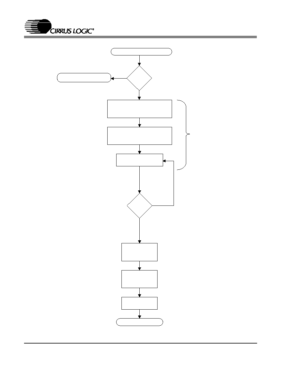
CS8920A Commits
Buffer Space to
Transmit Frame
Host Reads the BusST
Register (Register 18)
Transmit Request
Host Writes
Transmit Frame
to CS8920A
Host Writes Transmit Command
to the TxCMD Register
Host Writes Transmit Frame
Length to the TxLength Register
Exit Transmit Process
Yes
No
Enter Packet Transmit Process
Rdy4
TxNOW
bit = 1?
Polling Loop
No
Yes
Is
TxCMD
pending?
Exit: can't issue command
Note: Issuing a command
at this point will cause
previous transmit frame
to be lost.
CS8920A
Transmits Frame
Figure 5.12. Transmit Operation in Polling Mode
CS8920A
DS238PP2
111
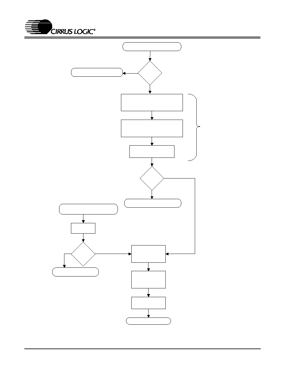
CS8920A Commits
Buffer Space to
Transmit Frame
Host Reads
ISQ
Host Reads the BusST
Register (Register 18)
Transmit Request
Host Writes
Transmit Frame
to CS8920A
Host Writes Transmit Command
to the TxCMD Register
Host Writes Transmit Frame
Length to the TxLength Register
Rdy4Tx
bit = 1?
Exit Transmit Process
No
Yes
No
Yes
Rdy4
TxNOW
bit = 1?
Host Enters Interrupt Routine
Exit WAIT-for-interrupt
Wait for next Interrupt
No
Yes
Is
TxCMD
pending?
Exit: can't issue command
Note: Issuing a command
at this point will cause
previous transmit frame
to be lost.
Enter Packet Transmit Process
CS8920A
Transmits Frame
Figure 5.13. Transmit Operation in Interrupt Mode
CS8920A
112
DS238PP2

memory to CS8920A memory using "REP" in-
struction (REP MOVS to memory base + 0A00h
i n memor y mo de, an d REP OUT t o R e-
ceive/Transmit Data Port (I/O base + 0000h) in
I/O mode).
5.8.7
Transmit in Interrupt Mode
In interrupt mode, Rdy4TxiE bit (Register B
"BufCFG", Bit 8) must be set for transmit opera-
tion. Transmit operation occurs in the following
order and is shown in Figure 5.13
1. The host bids for frame storage by writing the
Transmit Command to the TxCMD register
(memory base + 0144h in memory mode or
I/O base + 0004h in I/O mode).
2. The host writes the transmit frame length to the
TxLength register (memory base + 0146h in
memory mode or I/O base + 0006h in I/O
mode). If the transmit length is erroneous, the
command is discarded and the TxBidErr, bit
7, in BusST (Register 18) is set.
3. The host reads the BusST register. This read is
performed in memory mode by reading Regis-
ter 18, at memory base + 0138h. In I/O mode,
the host must first set the PacketPage Pointer
at the correct location by writing 0138h to the
PacketPage Pointer Port (I/O base + 000Ah),
it than can read the BusST register from the
PacketPage Data Port (I/O base + 000Ch).
After reading the register, the Rdy4TxNOW
bit is checked. If the bit is set, the frame can
b e wr it t en to CS 89 20A memory. If
Rdy4TxNOW is clear, the host will have to
wait for the CS8920A buffer memory to be-
come available at which time the host will be
interrupted. On interrupt, the host enters the
interrupt service routine and reads ISQ regis-
ter (Memory base + 0120h in memory mode
or I/O base + 0008h in I/O) and checks the
Rdy4Tx bit (bit 8). If Rdy4Tx is clear then
the CS8920A waits for the next interrupt. If
Rdy4Tx is set, then the CS8920A is ready to
accept the frame.
4. When the CS8920A is ready to accept the
frame, the host transfers the entire frame from
host memory to CS8920A memory using
"REP" instruction (REP MOVS to memory
base + 0A00h in memory mode, and REP
OUT to Receive/Transmit Data Port (I/O base
+ 0000h) in I/O mode).
5.8.8
Completing Transmission
When the CS8920A successfully completes
transmitting a frame, it sets the TxOK bit (Regis-
ter 8, TxEvent, Bit 8). If the TxOKiE bit
(Register 7, TxCFG, bit 8) is set, the CS8920A
generates a corresponding interrupt.
5.8.9
Rdy4TxNOW vs. Rdy4Tx
The Rdy4TxNOW bit (Register 18, BusST, bit 8)
is used to tell the host that the CS8920A is ready
to accept a frame for transmission. This bit is
used during the Transmit Request process or af-
ter the Transmit Request process to signal the
host that space has become available when inter-
rupts are not being used (i.e. the Rdy4TxiE bit
(Register B, BufCFG, Bit 8) is not set). Also, the
Rdy4Tx bit is used with interrupts and requires
the Rdy4TxiE bit be set.
Figures 5.12 & 5.13 provide diagrams of error
free transmission without collision.
For Revision B of CS8920A, if DMA mode is
used for receive operation, Rdy4Tx interrupt may
not occur every time. After servicing a RxDMA
interrupt, check the bit Rdy4TxNow to take ap-
propriate action.
5.8.10
Committing Buffer Space to a
Transmit Frame
When the host issues a transmit request, the
CS8920A checks the length of the transmit
CS8920A
DS238PP2
113

frame to see if there is sufficient on-chip buffer
space. If there is, the CS8920A sets the
Rdy4TxNOW bit. If not, and the Rdy4TxiE bit
is set, the CS8920A waits for buffer space to
free up and then sets the Rdy4Tx bit. If
Rdy4TxiE is not set, the CS8920A sets the
Rdy4TxNOW bit when space becomes available.
Even though transmit buffer space may be avail-
able, the CS8920A does not commit buffer space
to a transmit frame until all of the following are
true:
1. The host must issues a Transmit Request;
2. The Transmit Request must be successful; and,
3. Either the host reads that the Rdy4TxNOW bit
(Register 18, BusST, Bit 8) is set, or the host
reads that the Rdy4Tx bit (Register C,
BufEvent, bit 8) is set.
If the CS8920A commits buffer space to a par-
t ic u la r tr an smi t fra me , it will no t a llow
subsequent frames to be written to that buffer
space as long as the transmit frame is committed.
After buffer space is committed, the frame is
subsequently transmitted unless any of the fol-
lowing occur:
1. The host completely writes the frame data, but
transmission failed on the Ethernet line.
There are three such failures, and these are in-
dicated by three transmit error bits in the
TxEvent register (Register 8): 16coll, Jabber,
or Out-of-Window.
Or:
2. The host aborts the transmission by setting the
Force (Register 9, TxCMD, bit 8) bit. In this
case, the committed transmit frame, as well as
any yet-to-be-transmitted frames queued in
the on-chip memory, are cleared and not
transmitted. The host should make TxLength
= 0 when using the Force bit.
Or:
3. There is a transmit under-run, and the TxUn-
derrun bit (Register C, BufEvent, Bit 9) is set.
Successful transmission is indicated when the
TxOK bit (Register 8, TxEvent, Bit 8) is set.
Register 9, TxCMD
Host specified transmit length at 0146h (in bytes)
TxPadDis
(Bit D)
InhibitCRC
(Bit C)
3 < TxLength < 60
60 >= TxLength =< 1514 1514 > TxLength < 1518
TxLength > 1518
0
0
Pad to 60
and add CRC
Send frame and add
CRC [Normal Mode]
Will not send
Will not send
0
1
Pad to 60 and
send without CRC
Send frame
without CRC
Send frame
without CRC
Will not send
1
0
Send without pads,
and add CRC
Send frame
and add CRC
Will not send
Will not send
1
1
Send without pads
and without CRC
Send frame
without CRC
Send frame
without CRC
Will not send
NOTES: 1. If the TxPadDis bit is clear and InhibitCRC is set and the CS8920A is commanded to send a frame of
length less than 60 bytes, the CS8920A pads.
2. The CS8920A will not send a frame with TxLength less than 3 bytes.
Table 5.17. Transmit Frame Length
CS8920A
114
DS238PP2

5.8.11
Transmit Frame Length
The length of the frame transmitted is deter-
mined by the value written into the TxLength
register (PacketPage base + 0146h) during the
Transmit Request. The length of the transmit
frame may be modified by the configuration of
the TxPadDis bit (Register 9, TxCMD, Bit D)
and the InhibitCRC bit (Register 9, TxCMD, Bit
C). Table 5.17 defines how these bits affect the
length of the transmit frame. In addition, it
shows which frames the CS8920A will send.
5.9
Full Duplex Considerations
The driver should not bid to transmit a long
frame (i.e., a frame greater than 118 bytes) if the
prior transmit frame is still being transmitted.
The end of the transmission of this prior frame is
indicated by a TxOK bit being set in the
TxEvent register (register 8).
5.10
System Wakeup with Wakeup
Frames
The CS8920A will recognize a Magic Packet
wakeup frame that is received from either the
10BASE-T or AUI port, and can consequently
generate a signal to awaken a sleeping or idling
system CPU. A desktop system may go to sleep
in response to any number of conditions. For ex-
ample, a system power manager observes no user
or computing activity for some period of time, or
a user turns the PC off using a soft or hard
power switch.
Wakeup frame recognition allows access to a
sleeping (powered-down or slowed down) CPU
over the network. Potential applications include
personal remote access to a desktop PC, or ac-
cess by a host to all clients to upgrade software
programs, perform virus scans, or check for un-
authorized software.
A complete wakeup frame state diagram is
shown in Figure 5.14. The key states are as fol-
lows:
∑
NORMAL: The CS8920A is receiving nor-
mal packet traffic and is ignoring wakeup
frames.
∑
SUSPEND: The CS8920A is waiting for a
wakeup frame and is ignoring all other
frames. The ISA bus is powered down. Typi-
cally, the CPU is also powered down.
∑
STANDBY: The CS8920A is waiting for a
wakeup frame and is ignoring all other
frames. The ISA bus is powered up, and typi-
cally the CPU is running with a slowed-down
clock.
∑
RESET: The CS8920A is performing an in-
ternal reset and all received frames are
ignored. The state entered following RESET
is d e te rmi n ed b y t he con ten ts of the
EEPROM and by whether or not the ISA bus
is powered up.
∑
DROPPING FRAME: The CS8920A is look-
ing for normal packet traffic, but the ISA bus
is not powered up. This is a somewhat abnor-
mal condition.
Wakeup Frame Control/Status Bits
The following Control/Status bits are associated
with the wakeup function.
LineCTL (Register 13)
∑
bit F, WakeupEN: Set this bit to enable the
wakeup function. All non-wakeup frames are
discarded when wakeup is enabled. This bit
defaults to clear, meaning wakeup frame rec-
ognition is disabled. When recognition is
disabled, the EWAKE pin remains low inde-
pendent of the state of LineCTL, bit A.
CS8920A
DS238PP2
115

SUSPEND MODE
CS8920A ISA drivers are off
Ignoring normal frames
looking for wakeup
STANDBY MODE
CS8920A ISA drivers are on/active
Ignoring normal frames
looking for wakeup
NORMAL MODE
- ISA drivers on
- Looking for normal frames
- Ignoring wakeup frames
RESET = 1
or
ISA = off
ISA = on
and WakeupEn = 0, as read
from the EEPROM
RESET = 1
WakeupEn = 1
(from software
over the ISA bus)
WakeupEn = 0
(from software
over the ISA bus)
ISA = off
(causing reset = 1)
ISA = on
and
WakeupEn = 1
(from EEPROM)
ISA = off
and
WakeupEn = 1
(from the
EEPROM)
ISA = on
or RESET = 1
(qualified)
RESET STATE
CS8920A Inactive during reset
Read PPEROM
Normal frames are ignored
ISA = on
or
RESET = 1
(qualified)
Receive
Wakeup
frame
ASSERTING EWAKE
or GENERATE INTRQ
Deassert WakeupEn
DROPPING NORM
PACKETS
Ignoring wakeup frame
CS8920A drivers off
RxMiss occuring
ASSERT EWAKE
ISA = on
or
RESET = 1
(qualified)
Receive
Wakeup
frame
ISA = off
or
RESET = 0
ISA = off
and
WakeupEn = 0
(from EEPROM)
RESET is defined as an ISA bus reset signal.
ISA off is defined as the sensing of the ISA signals in the power off state.
This is accomplished when MEMR_b = MEMW_b = IOR_b = 0, which can only happen when the ISA bus is power off.
Figure 5.14.Wakeup Frame State Diagram
CS8920A
116
DS238PP2

∑
bit A, RouteWakeup: Set this bit to route the
wakeup signal to both the presently pro-
grammed interrupt pin and the EWAKE pin.
This bit defaults to clear, meaning the
wakeup signal is routed only to the EWAKE
pin. Note that the interrupt pin is used only if
the CS8920A has determined that the ISA
bus is powered up.
RxEvent (register 4) and ISQ
∑
bit F, Wakeup frame received: This bit is set
when a valid wakeup frame is received. This
bit is cleared when read. It may be set again
only by a new wakeup frame.
For more information about the status and con-
trol bits, see Section 4.4.1
NORMAL State
While in the NORMAL state, The CS8920A re-
ceives all packets and does not check for wakeup
frames. The CS8920A remains in NORMAL
state until a reset occurs or until the software sets
the WakeupEN bit to 1. The reset causes the
CS8920A to enter the RESET state. Setting
WakeupEN to 1 causes the CS8920A to enter the
STANDBY state.
While in the NORMAL state, and before enter-
ing the STANDBY state, the CS8920A must be
initialized with the following information:
∑
IA must be loaded into the CS8920A.
∑
RxCTL (Register 5) must be set for appropri-
ate address filtering set.
∑
LineCTL (Register 13) bit 7, SerRxOn, must
be set. This turns on the receiver.
∑
The RouteWakeup bit (LineCTL, bit A) must
be configured.
∑
If an interrupt is being used, an Interrupt Pin
must be enabled via BusCTL, register 17, bit
F.
If the CS8920A is to enter the SUSPEND or
STANDBY state from the RESET mode, then
during the NORMAL state, the software must
ensure that the EEPROM initialization section
contains the following:
∑
WakeupEn bit set to 1 (Reg 13, LineCTL, bit
F).
∑
Individual Address
∑
RxCTL (Register 5) must be set for appropri-
ate address filtering set.
∑
LineCTL (Register 13) bit 7, SerRxOn, must
be set. This turns on the receiver.
∑
The RouteWakeup bit (LineCTL, bit A) must
be configured.
If the CS8920A enters the STANDBY state from
the RESET state, the driver may select an Inter-
rupt pin via the BusCTL register, bit F after the
reset. Selecting the Interrupt pin via the
EEPROM may interfere with PnP configuration
management.
RESET State
The CS8920A enters the RESET state in re-
sponse to one of the following:
∑
The ISA bus reset signal is recognized. Note
that if the CS8920A has previously recog-
nized that the ISA bus was powered down,
the CS8920A qualifies a reset request by 15
transitions on MEMR. This qualification fil-
ters spurious signals on the reset pin.
∑
A reset request is written to bit 6 of register
SelfCTL (register 15).
CS8920A
DS238PP2
117

∑
The ISA bus transitions from powered up to
powered down. When the ISA bus is being
powered down and is decaying to ground, the
ISA reset signal may be asserted. At this
time, the CS8920A will reset. Therefore, be-
fore powering down the ISA bus, the
CS8920A EEPROM should be configured to
allow the CS8920A to be activated in wait-
ing-for-wakeup-frame state.
Note that a "CTRL-ALT-DEL" does not reset the
ISA bus.
During the RESET state, the CS8920A does an
internal hardware reset, ignores all incoming
frames, and reads the EEPROM, includng the
burned-in IEEE address. During reset, the
CS8920A also shuts off the CS8920A ISA bus
drivers. The drivers remain off until MEMR and
MEMW and IOR have all gone high. Also, the
CS8920A does not allow ISA accesses before
EEPROM initialization.
Based on the state of the ISA bus (powered or
not powered), and based on the state of the
WakeupEN bit as read from the EEPROM, the
CS8920A will exit the RESET state and enter
one of the NORMAL, STANDBY, SUSPEND,
or DROPPING PACKETS states, as shown be-
low.
SUSPEND State
In the SUSPEND state, the ISA bus is powered
down, and the WakeupEN bit is set to 1. Typi-
cally, the CPU and chipset clocks will also be
stopped. In this state, the CS8920A remains
powered, discards all non-wakeup frames, and
shuts off the CS8920A ISA bus drivers.
Upon wakeup frame recognition, the CS8920A
generates a signal on the EWAKE pin that can be
connected by jumper to the system power man-
ager. An EWAKE output signal will be a logic
high for approximately 50 to 55 ms. The system
power manager function can then wake up the
system.
After generating the EWAKE signal, the
CS8920A checks that the ISA bus is still pow-
ered off, and that there is no reset request. If
these conditions are true, the CS8920A returns to
the SUSPEND state. Otherwise, the CS8920A
enters the RESET state. Note that the CS8920A
determines that the ISA bus is powered by look-
ing for MEMR and MEMW and IOR bus signals
being simultaneously low.
In a system with a powered down ISA bus, inter-
rupts must not be enabled (via loading register
17, BusCTL register, bit F from the EEPROM).
STANDBY State
In the STANDBY state, the ISA bus is powered
up, and the CPU is typically operating at a low
clock rate to save power. This state is entered
when either:
∑
the CS8920A is in NORMAL state, and the
software sets WakeupEN bit to 1; or
∑
while in RESET state, the CS8920A detects
that the ISA bus is powered and the Wakeu-
pEN bit is set to 1 by the EEPROM.
In this state, the CS8920A is powered up, looks
for wakeup frame, and discards all other frames.
Upon wakeup frame recognition, the CS8920A
can wake up the CPU using either just the
EWAKE pin, or a combination of the EWAKE
pin and an ISA-bus interrupt.
State Entered
WakeupEN bit
from EEPROM
ISA bus
NORMAL
0
powered
DROPPING
PACKET
0
not powered
SUSPEND
1
not powered
STANDBY
1
powered
CS8920A
118
DS238PP2

For the CS8920A to signal a wakeup interrupt,
the RouteWakeup bit (LineCTL, register 13, bit
A) must be set, and the ISA bus must be pow-
ered up. When a wakeup frame is recognized, the
presently programmed interrupt pin remains as-
serted until the interrupt has been acknowledged
by reading the ISQ. The host is responsible for
determining the interrupt cause. The wakeup in-
terrupt signal meets all ISA bus requirements for
interrupt signals.
After the wakeup signals are generated, the
CS8920A will automatically reset the WakeupEN
bit to 0 and return to NORMAL state. alterna-
tively, the CS8920A will transition from the
STANDBY state to the reset state at any time if
the ISA bus transitions to powered down or if a
reset signal is recognized.
DROPPING PACKETS State
The CS8920A will enter the DROPPING PACK-
ETS state after reset if the ISA bus is not
powered, and if WakeupEN is off. The CS8920A
will look for normal frames, ignore wakeup
frames, and shut off the CS8920A ISA bus driv-
ers. Therefore, the CS8920A will not pass
received frames to the CPU. This state is exited
and the RESET state is entered upon detecting
that the ISA bus in now powered, or upon reset
signal recognition.
Definition of a Magic Packet Wakeup Frame
A received wakeup frame must pass the pres-
ently selected CS8920A destination address
filter. Typically, the frame will be a broadcast
frame because broadcast frames can pass through
routers, even if the IA is not present in the router
address tables. The payload of the frame must
contain at least six contiguous synchronization
bytes (six repetitions of FFh) followed immedi-
ately by sixteen repetitions of the 6-byte IA, with
no unused bits between successive IA occur-
rences. This information can appear anywhere in
the payload, but must be byte aligned. The
CS8920A uses the six FF bytes to determine
when to begin the address match.
A wakeup frame may contain multiple occur-
rences of the "six FFh + sixteen IA" pattern. The
CS8920A checks each pattern for an IA match.
Multiple patterns allow both the burned-in IEEE
IA and also a locally-administered IA to be
broadcast. The CS8920A compares the address
in the pattern with the contents of the IA address
register (located at PacketPage base + 0158h), to
determine if the PC should be awakened. In
STANDBY state, the PacketPage location will
contain a locally administered IA if such an ad-
dress has been loaded by the driver. Note that
upon entering the SUSPEND state (stopped ISA
bus), the PacketPage location will always contain
the burned-in IEEE address.
Use of Magic Packet Trade Mark
Customers who use the CS8920A Magic Packet
capability in their products are requested to use
the Magic Packet
TM
trademark in their applicable
sales and advertising documentation. Any cus-
tomer referring to Magic Packet in their literature
should attribute ownership of the trademark to
AMD, and should contact AMD for attribution
instructions.
Considerations for Hardware Design
Systems which implement wakeup-via-LAN will
generally use a seperate power supply for the
CS8920A. Please contact Crystal for board
deisgn guidelines.
CS8920A
DS238PP2
119

6.0
TEST MODES
Loopback & Collision Diagnostic Tests
Internal and external Loopback and Collision
tests can be used to verify the CS8920A's func-
tionality when configured for either 10BASE-T
or AUI operation.
Internal Tests
Internal tests allow the major digital functions to
be tested, independent of the analog functions.
During these tests, the Manchester encoder is
connected to the decoder. All digital circuits are
operational, and the transmitter and receiver are
disabled.
External Tests
External test modes allow the complete chip to
be tested without connecting it directly to an
Ethernet network.
Loopback Tests
During Loopback tests, the internal Carrier Sense
(CRS) signal, used to detect collisions, is ig-
nored, allowing packet reception during packet
transmission.
10BASE-T Loopback and Collision Tests
10BASE-T Loopback and Collision Tests are
controlled by two bits: Force FDX (Register 1D,
AutoNegCTL, Bit F) and ENDECloop (Register
19, TestCTL, Bit 9). Table 6.1 describes these
tests.
AUI Loopback and Collision Tests
AUI Loopback and Collision tests are controlled
by two bits in the Test Control register: AUIloop
(Register 19, TestCTL, Bit A) and ENDECloop
(Register 19, TestCTL, Bit 9). Table 6.2 de-
scribes these tests.
Test Mode
FDX
ENDECloop
Description of Test
10BASE-T Internal
Loopback
1
1
Transmit a frame and verify that the frame is received without error.
10BASE-T
Internal
Collision
0
1
Transmit frames and verify that collisions are detected and that
internal counters function properly. After 16 collisions, verify that
16coll (Register 8, TxEvent, Bit F) is set.
10BASE-T
External Loopback
1
0
Connect TXD+ to RXD+ and TXD- to RXD-. Transmit a frame and
verify that the frame is received without error.
10BASE-T
External
Collision
0
0
Connect TXD+ to RXD+ and TXD- to RXD-. Transmit frames and
verify that collisions are detected and that internal counters function
properly. After 16 collisions, verify that 16coll (Register 8, TxEvent,
Bit F) is set.
Table 6.1. 10BASE-T Loopback and Collision Tests
CS8920A
120
DS238PP2

6.1
Boundary Scan
Boundary Scan test mode provides an easy and
efficient board-level test for verifying that the
CS8920A has been installed properly. Boundary
Scan will check to see if the orientation of the
chip is correct, and if there are any open or short
circuits.
Boundary Scan is controlled by the TEST pin.
When TEST is high, the CS8920A is configured
for normal operation. When TEST is low, the
following occurs:
∑
the CS8920A enters Boundary Scan test
mode and stays in this mode as long as
TEST is low;
∑
the CS8920A goes through an internal reset
and remains in internal reset as long as
TEST is low;
∑
the AEN pin, normally the ISA bus Address
Enable, is redefined to become the Boundary
Scan shift clock input; and
∑
all digital outputs and bi-directional pins are
placed in a high-impedance state (this electri-
cally isolates the CS8920A digital outputs
from the rest of the circuit board).
For Boundary Scan to be enabled, AEN must be
low before TEST is driven low.
A complete Boundary Scan test is made up of
two separate cycles. The first cycle, known as the
Output Cycle, tests all digital output pins and all
bi-directional pins. The second cycle, known as
the Input Cycle, tests all digital input pins and all
bi-directional pins.
Output Cycle
During the Output Cycle, the falling edge of
AEN causes each of the 26 digital output pins
and each of the 16 bi-directional pins to be
driven low, one at a time. The cycle begins with
LINKLED and advances in order counterclock-
wise around the chip though all 42 pins. This test
is referred to as a "walking 0" test.
The following is a list of output pins and bi-di-
rectional pins that are tested during the Output
Cycle:
Pin Name
Pin #
Pin Name
Pin #
EECS
141
IRQ2/9
106
EESK
142
IRQ7
79
LOCALLED
5
IRQ6
78
EEDO
6
IRQ5
77
DRQ7
9
IRQ4
76
DRQ6
14
IRQ3
75
DRQ5
16
IOCS16
43
CSOUT
8
MCS16
44
SD08-SD15
27-24,21-18
IOCHRDY
92
IRQ15
31
SD0 - SD7
96-99,102-105
IRQ14
30
BSTATUS
113
IRQ12
32
LINKLED
139
IRQ11
33
LANLED
140
IRQ10
34
EWAKE
3
Test Mode
AUIloop
ENDECloop
Description of Test
AUI Internal
Loopback
1
1
Transmit a frame and verify that the frame is received without error.
AUI External
Loopback
1
0
Connect DO+ to DI+ and D0- to DI-. Transmit a frame and verify
that the frame is received without error (since there is no collision
signal, an SQE error will occur).
AUI Collision
0
0
Start transmission and observe DO+/DO- activity. Input a 10 MHz
sine wave to CI+/CI- pins and observe collisions.
Table 6.2. AUI Loopback and Collision Tests
CS8920A
DS238PP2
121

The output pins not included in this test are:
Pin Name
Pin #
Pin Name
Pin #
DO+
121
TXD-
126
DO-
122
RES
131
TXD+
125
XTAL2
136
Input Cycle
During the Input Cycle, the falling edge of AEN
causes the state of each selected pin to be trans-
ferred to EEDO (that is, EEDO will be high or
low depending on the input level of the selected
pin). This cycle begins with SLEEP and ad-
vances clockwise through each of 37 input pins
(all digital input pins except for AEN) and each
of the 16 bi-directional pins, one pin at a time.
The following is a list of input pins and bi-direc-
tional pins that are tested during the Input Cycle:
Pin Name
Pin #
Pin Name
Pin #
EEDI
7
SA0 - SA11
58-66,80-82
DACK7
10
REFRESH
83
DACK6
15
SA12- SA16
84-88,
DACK5
17
IOR
89
SD08-SD15
27-24,21-18
IOW
90
MEMW
28
SD0 - SD7
96-99,
102-105
MEMR
29
RESET
114
SBHE
52
SLEEP
116
LA17-23
45-51
The input pins not included in this test are:
Pin Name
Pin #
Pin Name
Pin #
AEN
91
CI-
120
TEST
115
RXD+
129
DI+
117
RXD-
130
DI-
118
XTAL1
135
CI+
119
After the Input Cycle is complete, one more cy-
cle of AEN returns all digital output pins and
bi-directional pins to a high-impedance state.
Continuity Cycle
The combination of a complete Output Cycle, a
complete Input Cycle, and an additional AEN cy-
cle is called a Continuity Cycle. Each Continuity
Cycle lasts for 85 AEN clock cycles. The first
Continuity Cycle can be followed by additional
Continuity Cycles by keeping TEST low and
continuing to cycle AEN. When TEST is driven
high, the CS8920A exits Boundary Scan mode
and AEN is again used as the ISA-bus Address
Enable.
Figure 6.1 shows a complete Boundary Scan
Continuity Cycle.
Figure 6.2 shows Boundary Scan timing.
CS8920A
122
DS238PP2

ENTER BOUNDARY SCAN:
CS8920A resets, all digital
output pins and bi-directional
pins enter High-Z state,
and AEN becomes shift clock
AEN switches high
OUTPUT CYCLE
AEN switches low
Selected output
goes low
AEN switches high
34 cycles
INPUT CYCLE
AEN switches low
Selected input
copied out
to the
EEDataOut
pin
AEN switches high
50 cycles
All digital output pins and
bi-directional pins enters
High-Z state
TEST switches low (AEN must be low)
Not in Boundary Scan
Test Mode
AEN switches low
AEN switches high
EXIT BOUNDARY SCAN:
AEN becomes ISA bus
Address Enable
TEST switches high
Figure 6.1. Boundary Scan Continuity Cycle
CS8920A
DS238PP2
123
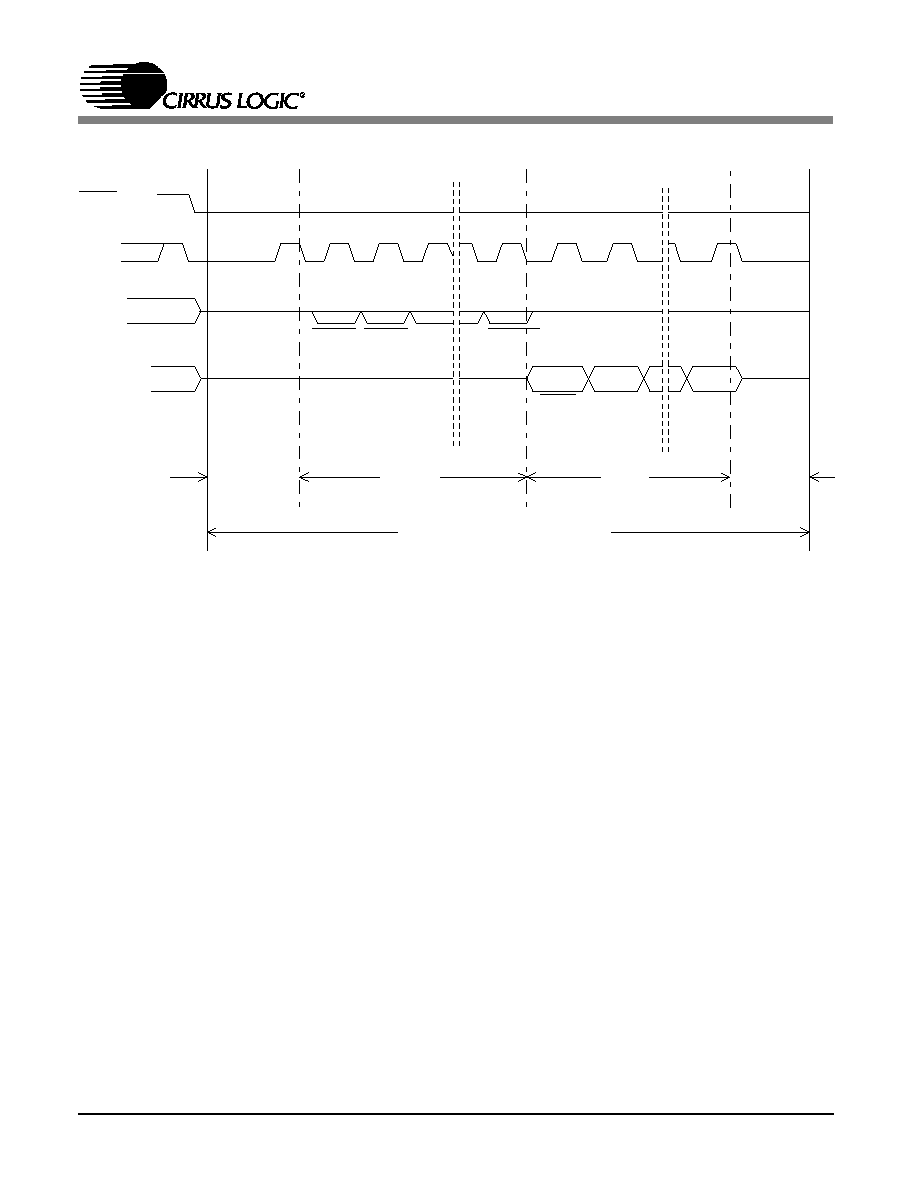
TEST
AEN
Outputs
All outputs
tri-state
LANLED
low
BSTATUS
low
EEDO
RESET
copied
out
OUTPUTS
Hi Z
OUTPUT
TEST
42 Clocks
INPUT
TEST
53 Clocks
OUTPUTS
Hi Z
1 clock
COMPLETE CONTINUITY CYCLE
96 Clocks
LINKLED
low
SLEEP
copied
out
EEDI
copied
out
Figure 6.2. Boundary Scan Timing
CS8920A
124
DS238PP2
7.0 ABSOLUTE MAXIMUM RATINGS
(AVSS, DVSS = 0 V, all voltages with respect to 0 V.)
Parameter
Symbol
Min
Max
Units
Power Supply:
Digital
Analog
D
V
DD
A
V
DD
-0.3
-0.3
6.0
6.0
V
V
Input Current
(Except Supply Pins)
±
10.0
mA
Analog Input Voltage
-0.3
(
A
V
DD+) +0.3
V
Digital Input Voltage
-0.3
(
D
V
DD+) +0.3
V
Ambient Temperature
(Power Applied)
-55
+125
∞
C
Storage Temperature
-65
+150
∞
C
Warning:
Operation at or beyond these limits may result in permanent damage to the device.
Normal operation is not guaranteed at these extremes.
8.0 RECOMMENDED OPERATING CONDITIONS
(AVSS, DVSS = 0 V, all voltages with respect to 0 V.)
Parameter
Symbol
Min
Max
Units
Power Supply:
Digital
Analog
D
V
DD
A
V
DD
4.75
4.75
5.25
5.25
V
V
Operating Ambient Temperature
T
A
0
+70
∞
C
9.0 DC CHARACTERISTICS
T
A
= 25 ∞C; Vdd = 5 V
Parameter
Symbol
Min
Max
Units
CRYSTAL (when using external clock)
XTAL1 Input Low Voltage
V
IXH
-0.3
0.8
V
XTAL1 Input High Voltage
V
IXH
3.5
V
DD
V
XTAL1 Input Low Current
I
IXL
-40
µ
A
XTAL1 Input High Current
I
IXH
40
µ
A
POWER SUPPLY
Power Supply Current while Active
I
DD
130
mA
Hardware Standby Mode Current
(Note 1) I
DDSTNDBY
1.0
mA
Hardware Suspend Mode Current
(Note 1) I
DDHWSUS
75
µ
A
Software Suspend Mode Current
(Note 1) I
DDSWSUS
1.0
mA
Notes:
1. With digital inputs connected to CMOS levels.
CS8920A
DS238PP2
125

9.0 DC CHARACTERISTICS (continued.)
I/O
Type
Parameter
Symbol
Conditions and
Comments
Min
Max
Units
DIGITAL INPUTS and OUTPUTS
OD24
Output Low Voltage
V
OL
I
OL
= 24 mA
0.4
V
OD24
Output Leakage Current
I
LL
0
V
OUT
V
CC
-10
10
µ
A
OD10
Output Low Voltage
V
OL
I
OL
= 10 mA
0.4
V
OD10
Output Leakage Current
I
LL
0
V
OUT
V
CC
-10
10
µ
A
B24
Output Low Voltage
V
OL
I
OL
= 24 mA
0.4
V
B24
Output High Voltage
V
OH
I
OH
= -12 mA
2.4
V
B24
Output Leakage Current
I
LL
0
V
OUT
V
CC
-10
10
µ
A
B4w
Output Low Voltage
V
OL
I
OL
= 4 mA
0.4
V
B4w
Output High Voltage
V
OH
IOH = -2 mA
2.4
V
B4w
Output Leakage Current
I
LL
0
V
OUT
V
CC
-20
10
µ
A
O24ts
Output Low Voltage
V
OL
I
OL
= 24 mA
0.4
V
O24ts
Output High Voltage
V
OH
I
OH
= -2 mA
2.4
V
O24ts
Output Leakage Current
I
LL
0
V
OUT
V
CC
-10
10
µ
A
O4
Output Low Voltage
V
OL
I
OL
= 4 mA
0.4
V
O4
Output High Voltage
V
OH
I
OH
= -2 mA
2.4
V
I
Input Low Voltage
V
IL
0.8
V
I
Input High Voltage
V
IH
2.4
V
I
Input Leakage Current
I
L
0
V
IN
V
CC
-10
10
µ
A
Iw
Input Low Voltage
V
IL
0.8
V
Iw
Input High Voltage
V
IH
2.4
V
Iw
Input Leakage Current
I
L
0
V
IN
V
CC
-20
10
µ
A
Pin Types:
d
=
Differential Input Pair
I
=
Input
G
=
Ground
dO =
Differential Output Pair
O
=
Output
ts
=
Tri-State
B
=
Bi-Directional with Tri-State Output
P
=
Power
w
=
Internal Weak Pullup
OD =
Open Drain Output
Digital outputs are followed by drive in mA (Example: OD24 = Open Drain Output with 24 mA drive).
CS8920A
126
DS238PP2

9.0 DC CHARACTERISTICS (continued)
Parameter
Symbol
Min
Typical
Max
Units
10BASE-T INTERFACE
Transmitter Differential Output Voltage (Peak)
V
OD
2.2
2.8
V
Receiver Normal Squelch Level (Peak)
V
ISQ
300
525
mV
Receiver Low Squelch Level (LoRxSquelch bit set)
V
SQL
125
290
mV
AUI INTERFACE
Transmitter Differential Output Voltage (DO+/DO- Peak)
V
AOD
±
0.45
±
1.2
V
Transmitter Undershoot Voltage
V
AODU
100
mV
Transmitter Differential Idle Voltage (DO+/DO- Peak)
V
IDLE
40
mV
Receiver Squelch Level (DI+/DI- Peak)
V
AISQ
180
300
mV
9.1 CAPACITANCE
T
A
= 25 ∞C; fc = 1 MHz; Vcc = 5 V
Limits
Parameter
Symbol
Min
Typical
Max
Unit
Test Condition
Input pins
C
IN
-
-
10
pF
All pins except pin under
test tied to AC ground
Input pins
C
OUT
-
-
20
pF
Input/Output Pins
C
IO
-
-
20
pF
CS8920A
DS238PP2
127
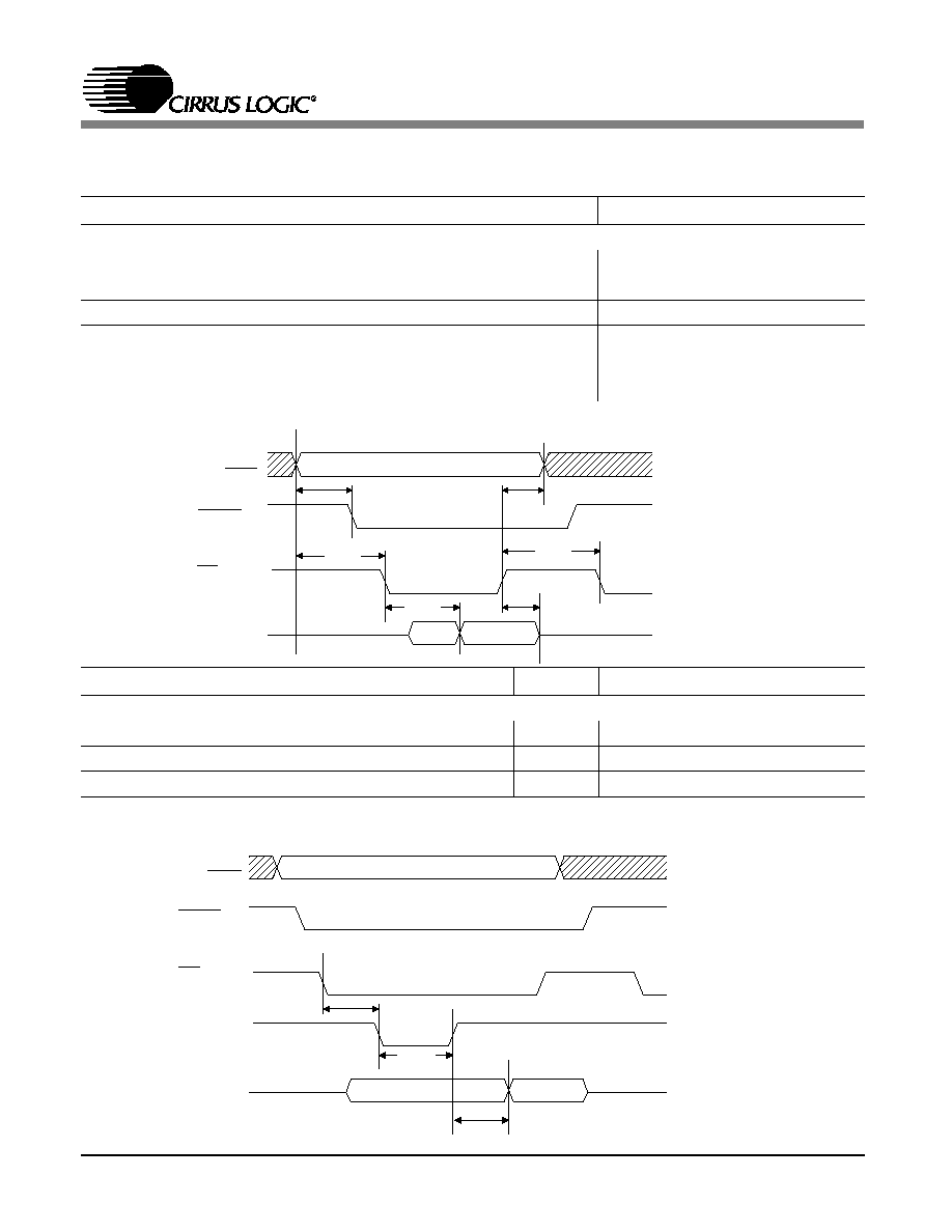
10.0 SWITCHING CHARACTERISTICS
T
A
= 25 ∞C; Vdd = 5 V
Parameter
Symbol
Min
Max
Units
16-BIT I/O READ, IOCHRDY NOT USED
Address, AEN, SBHE active to IOCS16 low
t
IOR1
35
ns
Address, AEN, SBHE active to IOR active
t
IOR2
20
ns
IOR low to SD valid
t
IOR3
145
ns
Address, AEN, SBHE hold after IOR inactive
t
IOR4
15
ns
IOR inactive to active
t
IOR5
60
ns
IOR inactive to SD 3-state
t
IOR6
30
ns
Parameter
Symbol
Min
Max
Units
16-BIT I/O READ, WITH IOCHRDY
IOR active to IOCHRDY inactive
t
IOR7
25
ns
IOCHRDY low pulse width
t
IOR8
125
175
ns
IOCHRDY active to SD valid
t
IOR9
0
ns
SA [16:0],
AEN, SBHE
Valid Address
IOCS16
IN
DIRECTION:
IN or OUT of chip
IOR
SD [15:0]
Valid Data
OUT
IN
OUT
t
IOR1
t
IOR2
t
IOR3
t
IOR4
t
IOR5
t
IOR6
SA [16:0],
AEN, SBHE
Valid Address
IOCS16
IN
DIRECTION:
IN or OUT of chip
IOR
SD [15:0]
Valid Data
OUT
IN
OUT
IOCHRDY
OUT
t
IOR7
t
IOR8
t
IOR9
CS8920A
128
DS238PP2

10.0 SWITCHING CHARACTERISTICS (continued)
Parameter
Symbol
Min
Max
Units
16-BIT MEMORY READ, IOCHRDY NOT USED
SA [16:0], SBHE, CHIPSEL, active to MEMCS16 low (Note 1)
t
MEMR1
30
ns
Address, SBHE, CHIPSEL active to MEMR active
t
MEMR2
20
ns
MEMR low to SD valid
t
MEMR3
145
ns
Address, SBHE, CHIPSEL hold after MEMR inactive
t
MEMR4
0
ns
MEMR inactive to SD 3-state
t
MEMR5
30
ns
MEMR inactive to active
t
MEMR6
55
ns
Parameter
Symbol
Min
Max
Units
16-BIT MEMORY READ, WITH IOCHRDY
MEMR low to IOCHRDY inactive
t
MEMR7
35
ns
IOCHRDY low pulse width
t
MEMR8
125
175
ns
IOCHRDY active to SD valid
t
MEMR9
0
ns
SA [16:0],
SBHE,
CHIPSEL
Valid Address
MEMCS16
IN
DIRECTION:
IN or OUT of chip
MEMR
SD [15:0]
Valid Data
OUT
IN
OUT
IOCHRDY
OUT
t
MEMR7
t
MEMR8
t
MEMR9
SA [16:0],
SBHE,
CHIPSEL
Valid Address
MEMCS16
IN
DIRECTION:
IN or OUT of chip
MEMR
SD [15:0]
Valid Data
OUT
IN
OUT
t
MEMR1
t
MEMR2
t
MEMR3
t
MEMR4
t
MEMR5
t
MEMR6
Note 1: It is assumed that the address line LA[23:17] has been latched early with BALE.
CS8920A
DS238PP2
129
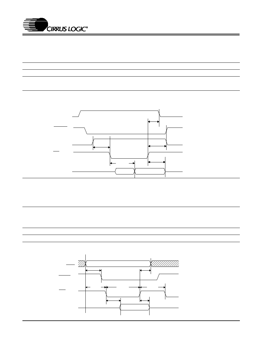
10.0 SWITCHING CHARACTERISTICS (continued)
Parameter
Symbol
Min
Max
Units
DMA READ
AEN active to IOR low
t
DMAR1
20
ns
IOR low to DMARQx inactive
t
DMAR2
80
ns
IOR low to SD valid
t
DMAR3
145
ns
DMACKx, AEN hold after IOR high
t
DMAR4
20
ns
IOR inactive to SD 3-state
t
DMAR5
30
ns
Parameter
Symbol
Min
Max
Units
16-BIT I/O WRITE
Address, AEN, SBHE valid to IOCS16 low
t
IOW1
35
ns
Address, AEN, SBHE valid to IOW low
t
IOW2
25
ns
IOW pulse width
t
IOW3
110
ns
SD hold after IOW high
t
IOW4
6
ns
IOW low to SD valid
t
IOW5
10
ns
IOW inactive to active
t
IOW6
55
ns
Address hold after IOW high
t
IOW7
0
ns
DMARQx
DIRECTION:
IN or OUT of chip
DMACKx
SD [15:0]
Valid Data Out
OUT
IN
OUT
x = 0, 1, 2
AEN
IN
IOR
IN
t
DMAR1
t
DMAR3
t
DMAR4
t
DMAR5
t
DMAR2
SA [15:0],
AEN, SBHE
Valid Address
IOCS16
IN
DIRECTION:
IN or OUT of chip
IOW
SD [15:0]
Valid Data In
OUT
IN
IN
t
IOW1
t
IOW2
t
IOW3
t
IOW4
t
IOW5
t
IOW6
t
IOW7
CS8920A
130
DS238PP2
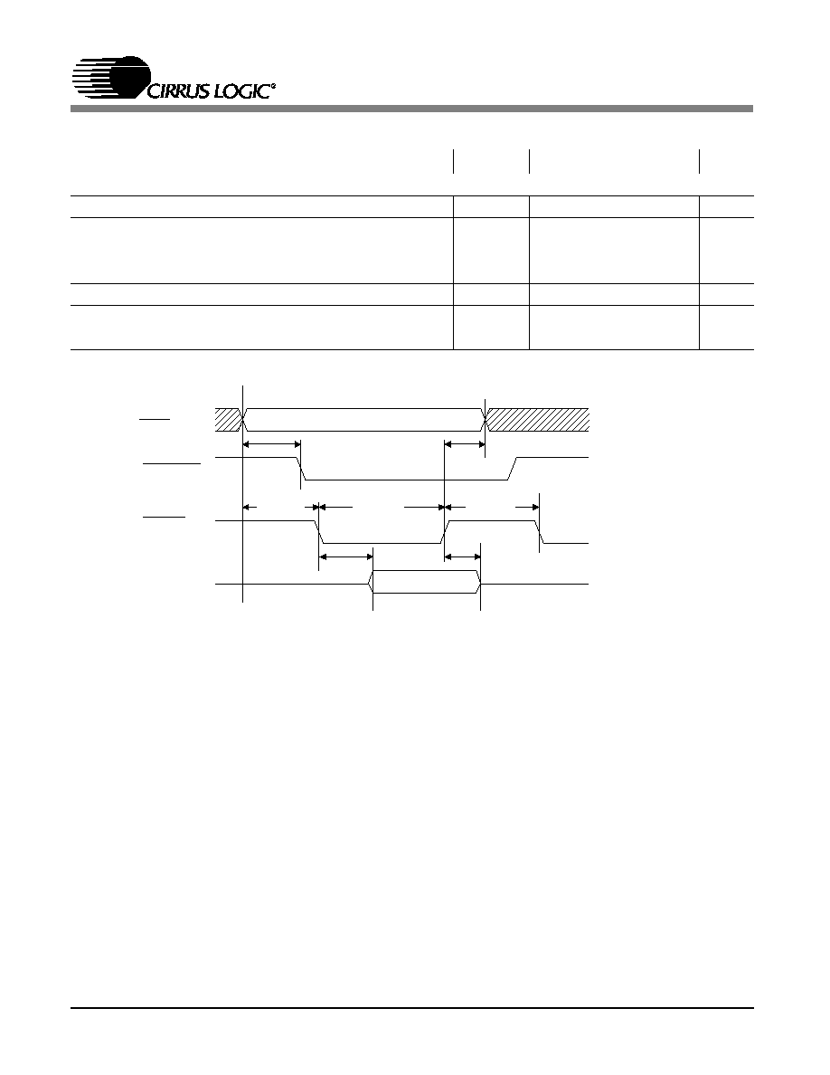
10.0 SWITCHING CHARACTERISTICS (continued)
Parameter
Symbol
Min
Max
Units
16-BIT MEMORY WRITE
Address, SBHE, valid to MEMCS16 low
(Note 1)
t
MEMW1
30
ns
Address, SBHE, valid to MEMW low
t
MEMW2
20
ns
MEMW pulse width
t
MEMW3
125
ns
MEMW low to SD valid
t
MEMW4
40
ns
SD hold after MEMW high
t
MEMW5
6
ns
Address hold after MEMW inactive
t
MEMW6
0
ns
MEMW inactive to active
t
MEMW7
55
ns
SA [16:0],
SBHE,
Valid Address
MEMCS16
IN
DIRECTION:
IN or OUT of chip
MEMW
SD [15:0]
Valid Data In
OUT
IN
IN
t
MEMW3
t
MEMW4
t
MEMW5
t
MEMW6
t
MEMW7
t
MEMW2
t
MEMW1
Note 1: It is assumed that the address line LA[23:17] has been latched early with BALE.
CS8920A
DS238PP2
131

10.0 SWITCHING CHARACTERISTICS (continued)
Parameter
Symbol
Min
Typ
Max
Units
10BASE-T RECEIVE
Allowable Received Jitter at Bit Cell Center
t
TRX1
±
13.5
ns
Allowable Received Jitter at Bit Cell Boundary
t
TRX2
±
13.5
ns
Carrier Sense Assertion Delay
t
TRX3
540
ns
Invalid Preamble Bits after Assertion of Carrier Sense
t
TRX4
1
2
bits
Carrier Sense Deassertion Delay
t
TRX5
270
ns
10.0 SWITCHING CHARACTERISTICS (continued)
Parameter
Symbol
Min
Typ
Max
Units
10BASE-T TRANSMIT
TXD Pair Jitter into 100 Ohm Load
t
TTX1
8
ns
TXD Pair Return to < 50 mV after Last Positive Transition
t
TTX2
4.5
µ
s
TXD Pair Positive Hold Time at End of Packet
t
TTX3
250
ns
tTRX3
RXD±
tTRX5
tTRX4
tTRX1
tTRX2
Carrier Sense (internal)
TXD±
tTTX1
tTTX3
tTTX2
CS8920A
132
DS238PP2
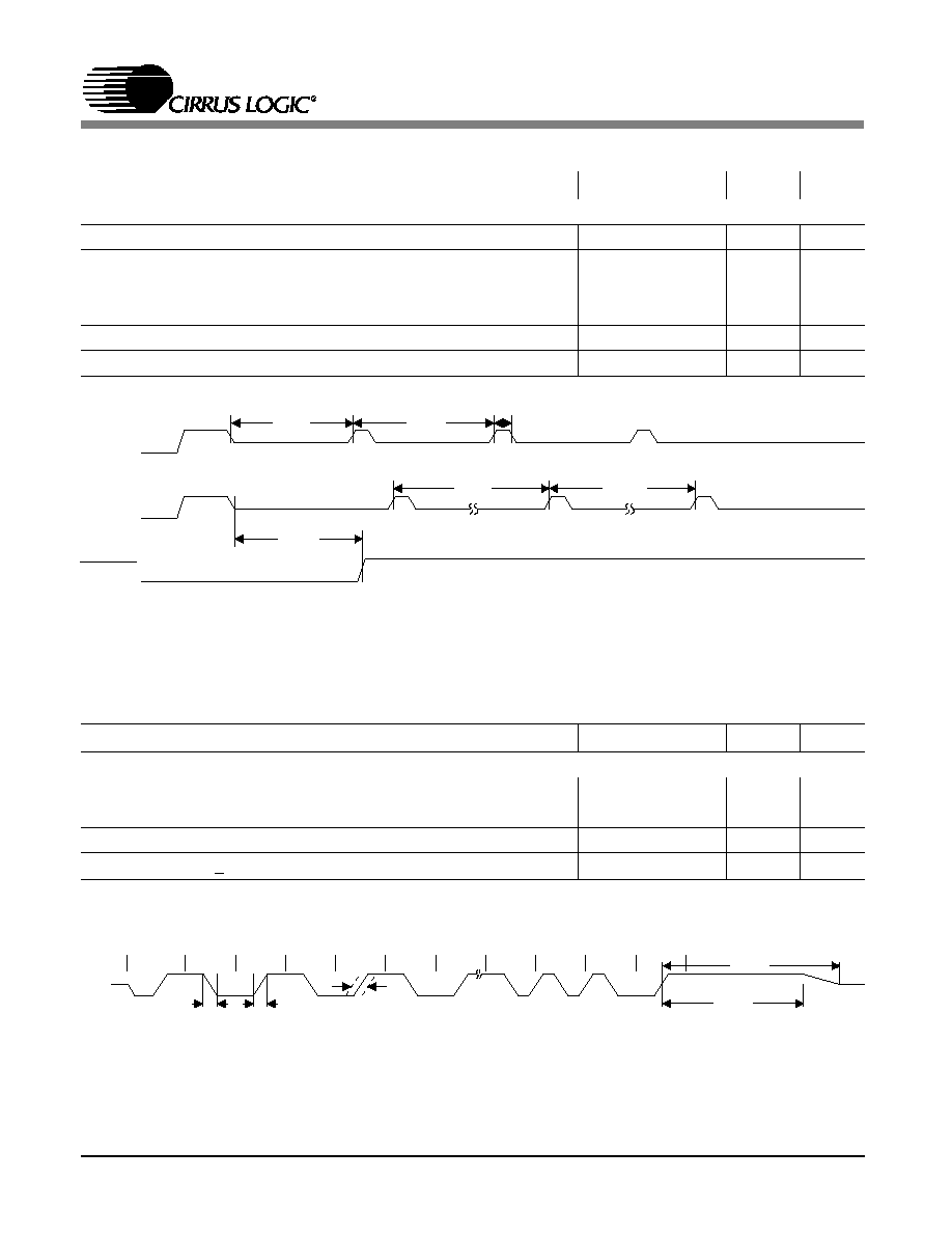
10.0 SWITHING CHARACTERISTICS (continued)
Parameter
Symbol
Min
Typ
Max
Units
10BASE-T LINK INTEGRITY
First Transmitted Link Pulse after Last Transmitted Packet
t
LN1
8
16
24
ms
Time Between Transmitted Link Pulses
t
LN2
8
16
24
ms
Width of Transmitted Link Pulses
t
LN3
60
100
200
ns
Minimum Received Link Pulse Separation
t
LN4
2
7
ms
Maximum Received Link Pulse Separation
t
LN5
25
150
ms
Last Receive Activity to Link Fail (Link Loss Timer)
t
LN6
50
150
ms
10.0 SWITHING CHARACTERISTICS (continued)
Parameter
Symbol
Min
Typ
Max
Units
AUI TRANSMIT
DO Pair Rise and Fall Times
t
ATX1
5
ns
DO Pair Jitter at Bit Cell Center
t
ATX2
0.5
ns
DO Pair Positive Hold Time at Start of Idle
t
ATX3
200
ns
DO Pair Return to < 40 mVp after Last Positive Transition
t
ATX4
8.0
µ
s
RXD±
LINKLED
TXD±
t
LN1
tLN2
t LN3
t
LN4
t
LN5
tLN6
DO±
tATX1
tATX1
tATX2
tATX4
tATX3
1
0
0
0
CS8920A
DS238PP2
133
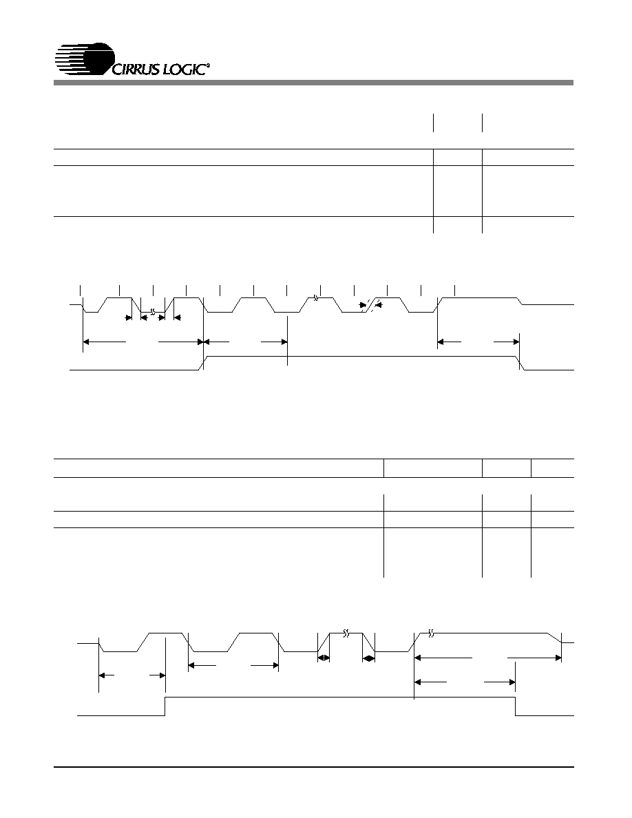
10.0 SWITCHING CHARACTERISTICS (continued)
Parameter
Symbol
Min
Typ
Max
Units
AUI RECEIVE
DI Pair Rise and Fall Time
t
ARX1
10
ns
Allowable Bit Cell Center and Boundary Jitter in Data
t
ARX2
±
18
ns
Carrier Sense Assertion Delay
t
ARX3
100
ns
Invalid Preamble Bits after Carrier Sense Asserts
t
ARX4
1
2
bits
Carrier Sense Deassertion Delay
t
ARX5
200
ns
10.0 SWITHING CHARACTERISTICS (continued)
Parameter
Symbol
Min
Typ
Max
Units
AUI COLLISION
CI Pair Cycle Time
t
ACL1
85
100
115
ns
CI Pair Rise and Fall Times
t
ACL2
10
ns
CI Pair Return to Zero from Last Positive Transition
t
ACL3
160
ns
Collision Assertion Delay
t
ACL4
140
ns
Collision Deassertion Delay
t
ACL5
240
ns
DI±
tARX1
tARX2
1
0
1
0
tARX3
tARX4
tARX5
tARX1
Carrier Sense (Internal)
t
ACL1
CI±
t
ACL4
t
ACL5
Collision (Internal)
t
ACL2
t
ACL2
t
ACL3
CS8920A
134
DS238PP2

10.0 SWITCHING CHARACTERISTICS (continued)
Parameter
Symbol
Min
Typ
Max
Units
External Boot PROM Access
Address active to MEMR
(Note 1) t
BPROM1
20
ns
MEMR active to CSOUT low
t
BPROM2
35
ns
MEMR inactive to CSOUT high
t
BPROM3
40
ns
10.0 SWITCHING CHARACTERISTICS (continued)
Parameter
Symbol
Min
Typ
Max
Units
EEPROM
EESK Setup time relative to EECS
t
SKS
100
-
-
ns
EECS/ELCS_b Setup time wrt
EESK
t
CSS
250
-
-
ns
EEDataOut Setup time wrt
EESK
t
DIS
250
-
-
ns
EEDataOut Hold time wrt
EESK
t
DIH
500
-
-
ns
EEDataIn Hold time wrt
EESK
t
DH
10
-
-
ns
EECS Hold time wrt
EESK
t
CSH
100
-
-
ns
SA [16:0]
MEMR
t BPROM1
CSOUT
CS
t BPROM3
t BPROM2
tCSH
tCS
tSKS
tCSS
tDIS
tDIH
tDH
EESK
EECS
EEData Out
EEData In
(Read)
Note 1: It is assumed that the address line LA[23:17] has been latched early with BALE.
CS8920A
DS238PP2
135
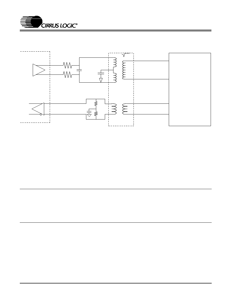
Rt
Rt
CS8900A
TD +
TD -
TXD +
TXD -
1 : 2
RJ45
1
2
1 : 1
RD +
RD -
3
6
0.01
µ
F
+
RXD+
RXD-
Rr
Rr
0.01
µ
F
-
68 pF
11.0 10BASE-T Wiring
Cable Impedance
(
)
Rt
(
)
Rr
(
)
100
24.3
49.9
120
30.1
60.4
150
37.4
75
NOTES:
1. If a center tap transformer is used on the RXD+ and RXD- inputs, replace the pair of Rr resistors
with a single 2xRr resistor.
2. The Rt and Rr resistors are +/- 1% tolerance.
3. The CS8920A supports 100, 120, and 150
unshielded twisted pair cables. The proper
values of Rt and Rr, for a given cable impedance, are shown below:
CS8920A
136
DS238PP2
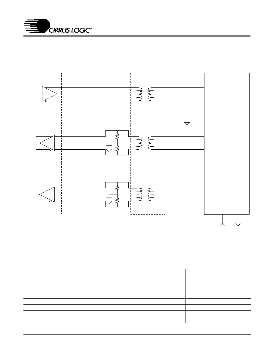
12.0 AUI Wiring
CS8900A
DO +
DO -
1 : 1
DB15
3
10
Tx
4
1 : 1
5
12
13
6
+12 V
+
CI +
C I -
1 : 1
2
9
39.2
39.2
Col
0.01 uF
-
+
DI +
D I -
39.2
39.2
Rx
0.01 uF
-
13.0 Quartz Crystal Requirements
If a 20 MHz quartz crystal is used, it must meet the following specifications:
Parameter
min
typ
max
unit
Parallel Resonant Frequency
20
MHz
Resonant Frequency Error (CL = 18 pF)
-50
+50
ppm
Resonant Frequency Change
Over Operating Temperature
-40
+40
ppm
Crystal Capacitance
18
pF
Motional Crystal Capacitance
0.022
pF
Series Resistance
50
Shunt Capacitance
7
pF
CS8920A
DS238PP2
137

MILLIMETERS
INCHES
0.007
0.854
0.049
0.000
MIN
0.063
0.008
MAX
0.011
0.018
0.030
0.008
DIM
D
D1
e
B
A
A1
L1
L
C
0∞
12∞
0.17
1.25
0.00
MIN
0.45
0.09
0∞
1.60
0.20
MAX
0.27
0.75
0.20
12∞
144-pin TQFP
21.70
0.004
14
4
1
E
D1
D
e
B
C
A1
A
L
Terminal
Detail 1
E
E1
22.30
21.70
-
22.30
0.878
0.854
0.878
1.00 REF
L1
E1
0.039 REF
NOM
1.43
0.10
0.22
0.65
0.15
22.00
20.00
22.00
20.00
-
-
-
0.40
0.60
0.50
-
NOM
0.056
0.004
0.009
0.024
0.006
0.866
0.787
0.866
0.787
0.020
-
0.016
0.024
-
-
-
-
14.0 PHYSICAL DIMENSIONS
Schematic & Layout Review Service
Confirm Optimum
Schematic & Layout
Before Building Your Board.
Confirm Optimum
Schematic & Layout
Before Building Your Board.
For Our Free Review Service
Call Applications Engineering.
For Our Free Review Service
Call Applications Engineering.
C a l l : ( 5 1 2 ) 4 4 5 - 7 2 2 2
CS8920A
138
DS238PP2

Glossary of Terms
Acronyms
AUI
Attachment Unit Interface
CRC
Cyclic Redundancy Check
CS
Carrier Sense
CSN
Card Select Number
CSMA/CD
Carrier Sense Multiple Access with Collision Detection
DA
Destination Address
EEPROM
Electrically Erasable Programmable Read Only Memory
EOF
End-of-Frame
FCS
Frame Check Sequence
FDX
Full Duplex
FLP
Fast Link Pulse
IA
Individual Address
IPG
Inter-Packet Gap
ISA
Industry Standard Architecture
LA
ISA Latchable Address Bus (LA17 - LA23)
LLC
Logical Link Control
MAC
Media Access Control
MAU
Medium Attachment Unit
MIB
Management Information Base
NLP
Normal Link Pulse
PnP
Plug and Play
RX
Receive
SA
Source Address or ISA System Address Bus (SA0 - SA19)
SFD
Start-of-Frame Delimiter
SNMP
Simple Network Management Protocol
SOF
Start-of-Frame
SQE
Signal Quality Error
STP
Shielded Twisted Pair
TCP/IP
Transmission Control Protocol/Internet Protocol
TDR
Time Domain Reflectometer
TX
Transmit
UTP
Unshielded Twisted Pair
Definitions
Cyclic Redundancy Check
The method used to compute the 32-bit frame check sequence (FCS).
Frame Check Sequence
The 32-bit field at the end of a frame that contains the result of the cyclic redundancy check
(CRC).
CS8920A
DS238PP2
139

Definitions (continued)
Frame
An Ethernet string of data bits that includes the Destination Address (DA), Source Address
(SA), optional length field, Logical Link Control data (LLC data), pad bits (if needed) and
Frame Check Sequence (FCS).
Individual Address
The specific Ethernet address assigned to a device attached to the Ethernet media.
Inter-Packet Gap
Time interval between packets on the Ethernet. Minimum interval is 9.6
µ
s.
Jabber
A condition that results when a Ethernet node transmits longer than between 20 ms and 150 ms.
Packet
An Ethernet string of data bits that includes the Preamble, Start-of-Frame Delimiter (SFD),
Destination Address (DA), Source Address (SA), optional length field, Logical Link Control
data (LLC data), pad bits (if needed) and Frame Check Sequence (FCS). A packet is a frame
plus the Preamble and SFD.
Receive Collision
A receive collision occurs when the CI+/CI- inputs are active while a packet is being received.
Applies only to the AUI.
Signal Quality Error
When transmitting on the AUI, the MAC expects to see a collision signal on the CI+/CI- pair
within 64 bit times after the end of a transmission. If no collision occurs, there is said to be an
"SQE error". Applies only to the AUI.
Slot Time
Time required for an Ethernet Frame to cross a maximum length Ethernet network. One Slot
Time equals 512 bit times.
Transmit Collision
A transmit collision occurs when the receive inputs, RXD+/RXD- (10BASE-T) or CI+/CI-
(AUI) are active while a packet is being transmitted.
CS8920A
140
DS238PP2

Acronyms Specific to the CS8920A
ADVintCTL/ST
Interrupt Control and Status - Register D
AutoNegST
ISA Bus State or Status - Register 1E
BufCFG
Buffer Configuration - Register B
BufEvent
Buffer Event - Register C
BusCTL
Bus Control - Register 17
BusST
Bus State - Register 18
ENDEC
Manchester encoder/decoder
ISQ
Interrupt Status Queue - register 0
LineCTL
Ethernet Line Control - Register 13
LineST
Ethernet Line Status - Register 14
RxCFG
Receive Configuration - Register 3
RxCTL
Receive Control - Register 5
RxEvent
Receive Event - Register 4
SelfCTL
Self Control - Register 15
SelfST
Self Status - Register 16
TestCTL
Test Control - Register 19
TxCFG
Transmit Configuration - Register 7
TxCMD
Transmit Command - Register 9
TxEvent
Transmit Event - Register 8
Terms Specific to the CS8920A
Act-Once bit
A control bit that causes the CS8920A to take a certain action once when a logic "1" is written
to that bit. To cause the action again, the host must rewrite a "1".
Committed Received Frame
A receive frame is said to be "committed" after the frame has been buffered by the CS8920A,
and the host has been notified, but the frame has not yet been transferred by the host.
Committed Transmit Frame
A transmit frame is said to be "committed" after the host has issued a Transmit Command, and
the CS8920A has reserved buffer space and notified the host that it is ready for transmit.
Event or Interrupt Event
The term "Event" is used in this document to refer to something that can trigger an interrupt.
Items that are considered "Events" are reported in the three Event registers (RxEvent, TxEvent,
or BufEvent) and in two counter-overflow bits (RxMISS and TxCOL).
CS8920A
DS238PP2
141

Terms Specific to the CS8920A (continued)
PacketPage
A unified, highly-efficient method of controlling and getting status of a peripheral controller in
I/O or Memory space.
Standby
A feature of the CS8920A used to conserve power. When in Standby mode, the CS8920A can
be awakened either by 10BASE-T activity or host command.
StreamTransfer
A method used to significantly reduce the number of interrupts to the host processor during
block data transfers (Patent Pending).
Suspend
A feature of the CS8920A used to conserve power. When in Suspend mode, the CS8920A can
be awakened only by host command.
Transfer
The term "transfer" refers to moving frame data across the ISA bus to or from the CS8920A.
Transmit Request
A Transmit Request is issued by the host to initiate the start of a new packet transmission. A
Transmit Request consists of the following three steps in exactly the order shown:
1. The host writes a Transmit Command to the TxCMD register (PacketPage base + 0144h).
2. The host writes the transmit frame's length to the TxLength register (PacketPage base +
0146h).
3. The host reads BusST (Register 18) to see in the Rdy4TxNOW bit (Bit 8) is set.
WakeUp Frame
A specific Ethernet frame that enables an NIC to signal the PC power management to power
up the PC.
Sub-Terms Specific to the CS8920A Used at the End of the Term
These terms have meaning only at the end of a term;
A
Accept
CMD
Command
CFG
Configure
CTL
Control
Dis
Disable
CS8920A
142
DS238PP2

E
Enable
h
Indicates the number is hexadecimal
iE
Interrupt Enable
ST
Status
CS8920A
DS238PP2
143