
CL-PD6833
Advance Data Sheet
June 1998
Version 0.3
PCI-to-CardBus Host Adapter
PCI
BUS
PC CARD SOCKET 1
PC CARD SOCKET 2
CL-PD6833
..................................
..................................
16 (R2)
or
32 (CardBus)
PC Card
..................................
..................................
16 (R2)
or
32 (CardBus)
PC Card
OVERVIEW
FEATURES
s
Pin-compatible with the CL-PD6832
s
PC 98 v1.0 and PC 97 compliant
s
Supports the
PCI Bus Power Management
Interface for PCI to CardBus Bridges
(PCMCIA
equivalent of ACPI) including PME# support
s
High-performance support for 133-Mbyte-per-
second transfers
s
ZV (zoomed video) port support for multimedia
applications using bypass mode
s
Programmable interrupt protocol: External
Hardware, PCI/Way, PCI, or PC/PCI interrupt
signalling modes
s
Up to four multiplexed general-purpose I/O pins
s
Seven fully programmable memory or I/O
windows per socket
s
Programmable per-socket activity indicators
s
Bus master capability
s
PCI 2.1, PCI 2.2 draft, PC Card Standard (March
1997), ExCA
TM,
and JEIDA 4.2 compliant
s
CL-PD672X register set compatible
s
Mixed-voltage support
s
Support for 5-V and 3.3-V PC Cards
The CL-PD6833 easily interfaces with the 8- and 16-bit
R2 PC Cards and the 32-bit CardBus PC Cards. It is
the third device to be developed in Cirrus Logic's family
of CardBus controllers. The CL-PD6833 gives system
designers of portable, notebook, and handheld
computers the most integrated solution for their needs.
Providing high performance, low-power consumption,
and a highly compatible and flexible interface, the
CL-PD6833 enables easy functionality for PC Card
and CardBus applications such as LANs, modems,
and multimedia applications.
The CL-PD6833 is a single-chip CardBus controller
capable of controlling two independent PC Card
and/or CardBus sockets. Featuring enhanced bus
traffic management and cycle pipelining technology,
the CL-PD6833 supports transactions at the PCI
specification limit of 133 Mbytes per second. This
significantly improves the performance over previous
Cirrus Logic controllers.
(cont.)
System Block Diagram
CL-PD6833
PCI-to-CardBus Host Adapter
OVERVIEW
(cont.)
The CL-PD6833 is compliant with the latest PC 97 and
PC 98 design guidelines. The CL-PD6833 is also
compliant with PCI 2.1, PCI 2.2 draft, PC Card
Standard (March 1997), ExCA
TM
, and JEIDA 4.2
standards. Like the CL-PD6834, the register set of the
CL-PD6833 is a superset of the Intel
Æ
365-SL, the
CL-PD672X, and the CL-PD6832 register sets; this
ensures full compatibility with existing card and socket
services software, thus maximizing PC software
compatibility.
The CL-PD6833 is compliant with the
PCI Bus Power
Management Interface for PCI to CardBus Bridges
,
which is the PCMCIA industry's document for ACPI
compatibility. The device is also compliant with the PC
Card controller Device Class Specification.
The CL-PD6833 uses state-of-the-art clock control to
satisfy industry power consumption targets, thereby
assuring minimum power consumption during the
various operational and suspend states. The device
also offers a Hardware Suspend mode, which is a
method of powering down the host controller to the
minimum power consumption levels in addition to
ACPI-compatible power management features.
The ACPI-compatible power management features of
the CL-PD6833 plus its state-of-the-ar t clock
management and hardware suspend modes ensure
that the system designer is provided with all the power
management control needed to implement an energy-
efficient, mixed-voltage CardBus controller.
Zoomed video support had become an important con-
sideration for system designers since 1996. The
CL-PD6833 can be programmed to tristate its PC Card
interface so that graphics and audio signals from a
zoomed video≠capable PC Card can be sent to the
respective graphics and audio controller zoomed video
ports. This solution is practical for multimedia applica-
tions such as DVD, full-motion video, and video confer-
encing.
The CL-PD6833 provides flexibility in non-PC
compatible applications by allowing easy translation of
PCI bus memory cycles to PC Card 16 I/O cycles for
processors with memory cycles only. In addition, the
CL-PD6833 has up to four multiplexed GPIO (general-
purpose I/O) pins to interface with external devices
that the system designer may wish to implement.
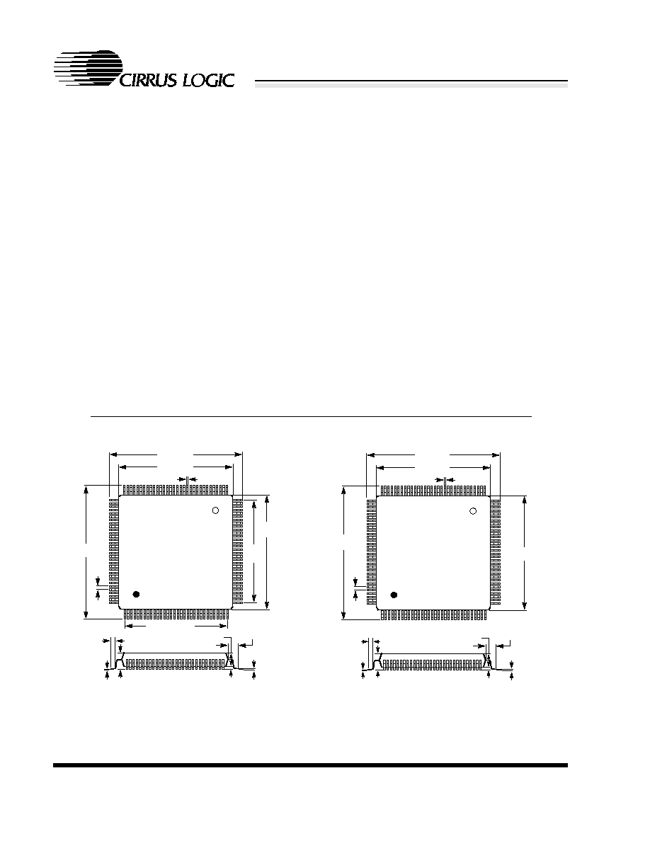
NOTES:
1)
Dimensions are in millimeters (inches), and controlling dimension is millimeter.
2)
The drawing above does not reflect exact package pin count.
3)
Before beginning any new design with this device, please contact Cirrus Logic for the latest package information.
PIN 1 INDICATOR
25.50 (1.004) REF
30.35 (1.195)
30.85 (1.215)
0.13 (0.005)
0.28 (0.011)
27.90 (1.098)
28.10 (1.106)
25.50
(1.004)
REF
0.50
(0.0197)
BSC
30.35 (1.195)
30.85 (1.215)
27.90 (1.098)
28.10 (1.106)
3.17 (0.125)
3.67 (0.144)
0
∞
MIN
7
∞
MAX
0.09 (0.004)
0.23 (0.009)
4.07
0.40 (0.016)
0.75 (0.030)
0.25
1.30 (0.051) REF
PIN 1
PIN 208
(0.160)
MAX
(0.010)
MIN
CL-PD6833
208-PIN MQFP
PIN 1 INDICATOR
29.60 (1.165)
30.40 (1.197)
0.17 (0.007)
0.27 (0.011)
27.80 (1.094)
28.20 (1.110)
0.50
(0.0197)
BSC
29.60 (1.165)
30.40 (1.197)
27.80 (1.094)
28.20 (1.110)
1.35 (0.053)
1.45 (0.057)
0
∞
MIN
7
∞
MAX
0.09 (0.004)
0.20 (0.008)
0.45 (0.018)
0.75 (0.030)
1.00 (0.039) BSC
PIN 1
PIN 208
CL-PD6833
208-PIN LQFP
1.40 (0.055)
1.60 (0.063)
0.05 (0.002)
0.15 (0.006)
Package Outline Drawings

June 1998
3
ADVANCE DATA BOOK v0.3
TABLE OF CONTENTS
CL-PD6833
PCI-to-CardBus Host Adapter
Table of Contents
1.
CONVENTIONS.......................................................................................................................7
2.
PIN INFORMATION .................................................................................................................9
2.1
Pin Diagrams........................................................................................................................................10
2.2
Pin Description Conventions ................................................................................................................12
2.3
Pin Descriptions ...................................................................................................................................13
3.
INTRODUCTION TO THE CL-PD6833..................................................................................25
3.1
System Architecture .............................................................................................................................25
3.1.1
PC Card Basics.......................................................................................................................25
3.1.2
CL-PD6833 R2 Windowing Capabilities..................................................................................26
3.1.3
Zoomed Video Port .................................................................................................................29
3.1.4
Interrupts .................................................................................................................................30
3.1.5
PCI/Way DMA .........................................................................................................................34
3.1.6
Power Management ................................................................................................................34
3.1.7
Socket Power Management Features .....................................................................................35
3.1.8
Bus Sizing ...............................................................................................................................37
3.1.9
Programmable PC Card Timing ..............................................................................................37
3.1.10 ATA Mode Operation ...............................................................................................................37
3.1.11 PC Card Sensing ....................................................................................................................37
3.2
Upgrading from the CL-PD6832 to the CL-PD6833.............................................................................38
3.2.1
Added Registers......................................................................................................................39
3.3
Host Access to Registers .....................................................................................................................42
3.4
Power-On Setup...................................................................................................................................44
4.
REGISTER DESCRIPTION CONVENTIONS.......................................................................45
5.
PCI CONFIGURATION REGISTERS....................................................................................47
5.1
Vendor ID and Device ID......................................................................................................................48
5.2
Command and Status ..........................................................................................................................49
5.3
Revision ID and Class Code ................................................................................................................52
5.4
Cache Line Size, Latency Timer, Header Type, and BIST ...................................................................53
5.5
Memory Base Address.........................................................................................................................54
5.6
CardBus Status ....................................................................................................................................55
5.7
PCI Bus Number, CardBus Number, Subordinate Bus Number, and CardBus Latency Timer ............57
5.8
Memory Base 0≠1 ................................................................................................................................58
5.9
Memory Limit 0≠1 ................................................................................................................................59
5.10 I/O Base 0≠1 ........................................................................................................................................60
5.11 I/O Limit 0≠1.........................................................................................................................................61
5.12 Interrupt Line, Interrupt Pin, and Bridge Control ..................................................................................62
5.13 Subsystem Vendor ID and Subsystem Device ID ................................................................................65
5.14 PC Card 16-Bit IF Legacy Mode Base Address...................................................................................66
5.15 Power Management Registers .............................................................................................................67
5.16 Power Management Control and Status ..............................................................................................68
5.17 DMA Slave Configuration Register.......................................................................................................70
5.18 Socket Number ....................................................................................................................................71
5.19 Configuration Miscellaneous 1 .............................................................................................................73

ADVANCE DATA BOOK v0.3
June 1998
4
TABLE OF CONTENTS
CL-PD6833
PCI-to-CardBus Host Adapter
6.
CARDBUS REGISTERS ...................................................................................................... 75
6.1
Status Event -- PME_CXT .................................................................................................................. 75
6.2
Status Mask -- PME_CXT................................................................................................................... 77
6.3
Present State ....................................................................................................................................... 78
6.4
Event Force .......................................................................................................................................... 80
6.5
Control -- PME_CXT ........................................................................................................................... 82
7.
OPERATION REGISTERS ................................................................................................... 85
7.1
Index .................................................................................................................................................... 85
7.2
Data...................................................................................................................................................... 90
8.
DEVICE CONTROL REGISTERS........................................................................................ 91
8.1
Chip Revision ....................................................................................................................................... 91
8.2
Interface Status .................................................................................................................................... 92
8.3
Power Control -- PME _CXT ............................................................................................................... 94
8.4
Interrupt and General Control -- PME_CXT........................................................................................ 96
8.5
Card Status Change -- PME_CXT ...................................................................................................... 98
8.6
Management Interrupt Configuration -- PME_CXT............................................................................. 99
8.7
Mapping Enable ................................................................................................................................. 101
9.
WINDOW MAPPING REGISTERS..................................................................................... 103
9.1
I/O Window Mapping Registers.......................................................................................................... 105
9.1.1
I/O Window Control ............................................................................................................... 105
9.1.2
System I/O Map 0≠1 Start Address Low ............................................................................... 107
9.1.3
System I/O Map 0≠1 Start Address High .............................................................................. 107
9.1.4
System I/O Map 0≠1 End Address Low ................................................................................ 108
9.1.5
System I/O Map 0≠1 End Address High ............................................................................... 108
9.1.6
Card I/O Map 0≠1 Offset Address Low ................................................................................. 109
9.1.7
Card I/O Map 0≠1 Offset Address High ................................................................................ 109
9.2
Memory Window Mapping Registers ................................................................................................. 110
9.2.1
System Memory Map 0≠4 Start Address Low....................................................................... 110
9.2.2
System Memory Map 0≠4 Start Address High...................................................................... 111
9.2.3
System Memory Map 0≠4 End Address Low ........................................................................ 112
9.2.4
System Memory Map 0≠4 End Address High ....................................................................... 113
9.2.5
Card Memory Map 0≠4 Offset Address Low ......................................................................... 114
9.2.6
Card Memory Map 0≠4 Offset Address High ........................................................................ 115
10. GENERAL WINDOW MAPPING REGISTERS.................................................................. 117
10.1 General Mapping Registers for I/O Mode .......................................................................................... 119
10.1.1 Gen Map 0≠6 Start Address Low (I/O).................................................................................. 119
10.1.2 Gen Map 0≠6 Start Address High (I/O)................................................................................. 120
10.1.3 Gen Map 0≠6 End Address Low (I/O) ................................................................................... 121
10.1.4 Gen Map 0≠6 End Address High (I/O) .................................................................................. 122
10.1.5 Gen Map 0≠6 Offset Address Low (I/O)................................................................................ 123
10.1.6 Gen Map 0≠6 Offset Address High (I/O) ............................................................................... 124
10.2 General Mapping Register for Memory Mode .................................................................................... 125
10.2.1 Gen Map 0≠6 Start Address Low (Memory) ......................................................................... 125
10.2.2 Gen Map 0≠6 Start Address High (Memory)......................................................................... 126
10.2.3 Gen Map 0≠6 End Address Low (Memory)........................................................................... 127
10.2.4 Gen Map 0≠6 End Address High (Memory) .......................................................................... 128
10.2.5 Gen Map 0≠6 Offset Address Low (Memory)........................................................................ 129
10.2.6 Gen Map 0≠6 Offset Address High (Memory)....................................................................... 130

June 1998
5
ADVANCE DATA BOOK v0.3
TABLE OF CONTENTS
CL-PD6833
PCI-to-CardBus Host Adapter
11. EXTENSION REGISTERS .................................................................................................131
11.1 Misc Control 1 ....................................................................................................................................132
11.2 FIFO Control ......................................................................................................................................134
11.3 Misc Control 2 ....................................................................................................................................136
11.4 Chip Information.................................................................................................................................137
11.5 ATA Control ........................................................................................................................................138
11.6 Extended Index ..................................................................................................................................140
11.7 Extended Data ...................................................................................................................................141
11.7.1 Extension Control 1...............................................................................................................142
11.7.2 Gen Map 0≠6 Upper Address (Memory) ...............................................................................143
11.7.3 Pin Multiplex Control 0 Register -- PME_CXT .....................................................................144
11.7.4 Pin Multiplex Control 1 Register -- PME_CXT .....................................................................146
11.7.5 GPIO Output Control.............................................................................................................147
11.7.6 GPIO Input Control................................................................................................................147
11.7.7 GPIO Output Data.................................................................................................................148
11.7.8 GPIO Input Data....................................................................................................................148
11.8 Prefetch Window Register ..................................................................................................................149
11.8.1 PCI Space Control ................................................................................................................149
11.8.2 PC Card Space Control.........................................................................................................150
11.8.3 Window Type Select ..............................................................................................................150
11.8.4 Misc Control 3 .......................................................................................................................151
11.8.5 SMBus Socket Power Control Address -- PME_CXT ..........................................................153
11.8.6 Gen Map 0≠6 Extra Control (I/O) ..........................................................................................154
11.8.7 Gen Map 0≠6 Extra Control (Memory) ..................................................................................155
11.8.8 Extension Card Status Change.............................................................................................156
11.8.9 Misc Control 4 .......................................................................................................................157
11.8.10 Misc Control 5 .......................................................................................................................158
11.8.11 Misc Control 6 .......................................................................................................................158
11.9 Device Identification and Implementation Scheme ............................................................................159
11.9.1 Mask Revision Byte...............................................................................................................159
11.9.2 Product ID Byte .....................................................................................................................160
11.9.3 Device Capability Byte A .......................................................................................................161
11.9.4 Device Capability Byte B .......................................................................................................162
11.9.5 Device Implementation Byte A ..............................................................................................163
11.9.6 Device Implementation Byte B ..............................................................................................164
11.9.7 Device Implementation Byte C ..............................................................................................165
11.9.8 Device Implementation Byte D ..............................................................................................166
12. TIMING REGISTERS...........................................................................................................167
12.1 Setup Timing 0≠1 ...............................................................................................................................167
12.2 Command Timing 0≠1 ........................................................................................................................168
12.3 Recovery Timing 0≠1 .........................................................................................................................169
13. DMA OPERATION REGISTERS.........................................................................................171
13.1 Low Address ......................................................................................................................................172
13.2 Mid Low Address................................................................................................................................172
13.3 Mid High Address...............................................................................................................................173
13.4 High Address......................................................................................................................................173
13.5 Low Count ..........................................................................................................................................174
13.6 Mid Count...........................................................................................................................................174
13.7 High Count .........................................................................................................................................174

ADVANCE DATA BOOK v0.3
June 1998
6
TABLE OF CONTENTS
CL-PD6833
PCI-to-CardBus Host Adapter
13.8 DMA Command and Status ............................................................................................................... 175
13.9 Request Register ............................................................................................................................... 176
13.10 Mode Register.................................................................................................................................... 177
13.11 Master Clear....................................................................................................................................... 178
13.12 Mask Register .................................................................................................................................... 178
14. ATA MODE OPERATION ................................................................................................... 179
15. ELECTRICAL SPECIFICATIONS ...................................................................................... 181
15.1 Absolute Maximum Ratings ............................................................................................................... 181
15.2 DC Specifications............................................................................................................................... 181
15.3 AC Timing Specifications ................................................................................................................... 185
15.3.1 PCI Bus Timing ..................................................................................................................... 186
15.3.2 System Interrupt Timing ........................................................................................................ 191
15.3.3 PC Card (PCMCIA) Bus Timing Calculations........................................................................ 192
15.3.4 PC Card (PCMCIA) Bus Timing ............................................................................................ 193
16. PACKAGE SPECIFICATIONS............................................................................................ 199
17. ORDERING INFORMATION .............................................................................................. 201
A.
PIN LISTINGS..................................................................................................................... 203
INDEX.................................................................................................................................. 211

June 1998
7
ADVANCE DATA BOOK v0.3
CONVENTIONS
CL-PD6833
PCI-to-CardBus Host Adapter
1.
CONVENTIONS
This section presents conventions used in this document.
General Conventions
Bits within words and words within various memory spaces are generally numbered with
0
(zero) as the
least-significant bit or word. For example, the least-significant bit of a byte is bit 0, and the most-significant
bit is bit 7.
In addition, number ranges for bit fields and words are presented with the most-significant value first. Thus,
when discussing a bit field within a register, the bit number of the most-significant bit is written first, followed
by a colon (:), and then the bit number of the least-significant bit; for example, bits 7:0.
In this document, the names of the CL-PD6833 internal registers are boldface. For example,
Chip Revision
and
Power Control
are register names. The names of bit fields are written with initial uppercase letters. For
example, Card Power On and Battery Voltage Detect are bit field names.
Abbreviations and Acronyms
The following table lists abbreviations and acronyms used in this document.
Acronym or
Abbreviation
Definition
AC
alternating current
ACPI
advanced configuration and power
interface
ATA
AT-attachment
CIS
card information structure
DAC
digital-to-analog converter
DC
direct current
DMA
direct memory access
EEPROM
electrically erasable/programmable
read-only memory
EEROM
electrically erasable read-only memory
GPIO
general-purpose I/O
IDE
integrated device electronics
IRQ
interrupt request
ISA
industry standard architecture
JEIDA
Japanese Electronic Industry
Development Association
LQFP
low-profile quad flat pack
LSB
least-significant bit
MQFP
metric quad flat pack
MSB
most-significant bit
MUX
multiplexer
PCI
peripheral component interconnect
PCM
pulse coded modulation
PCMCIA
Personal Computer Memory Card
International Association
PME
power management enable
R2
Release 2 (PC Card 16)
RFU
reserved for future use
RU
read update
SIC
serial interrupt controller
SMBus
TM
system management bus
VGA
video graphics array
ZV
zoomed video
Acronym or
Abbreviation
Definition
(cont.)

ADVANCE DATA BOOK v0.3
June 1998
8
CONVENTIONS
CL-PD6833
PCI-to-CardBus Host Adapter
Measurement Abbreviations
NUMBERS
Hexadecimal numbers are presented with all letters in uppercase and a lowercase h appended. For exam-
ple,
14h
and
03CAh
are hexadecimal numbers.
Binary numbers are enclosed in single quotation marks when in text. For example, `
11
' is a binary number.
Numbers not indicated by an
h
or single quotation marks are decimal.
The use of `tbd' indicates values that are `to be determined', `n/a' designates `not available', and `n/c' indi-
cates a pin that is a `no connect'.
In addition, an uppercase
X
is used within numbers to indicate digits ignored by the CL-PD6833 within the
current context. For example, `
101XX01'
is a binary number with bits 3:2 ignored.
Symbol
Units of measure
∞
C
degree Celsius
Gbyte
gigabyte (2
30
or 1,073,741,824 bytes)
Hz
hertz (cycle per second)
Kbyte
kilobyte (2
10
or 1,024 bytes)
kHz
kilohertz (1,000 hertz)
Mbyte
megabyte (2
20
or 1,048,576 bytes)
MHz
megahertz (1,000,000 hertz)
µ
A
microampere
µ
s
microsecond (1,000 nanoseconds)
mA
milliampere
ms
millisecond (1,000 microseconds)
ns
nanosecond
pF
picofarad
V
volt

June 1998
9
ADVANCE DATA BOOK v0.3
PIN INFORMATION
CL-PD6833
PCI-to-CardBus Host Adapter
2.
PIN INFORMATION
The CL-PD6833 is packaged in a 208-pin MQFP (formerly PQFP) or LQFP (formerly VQFP) component
package. The CL-PD6833 interface pins can be divided into four groups:
q
PCI bus interface pins
q
PC Card socket interface pins (two sets)
q
Power control and general interface pins
q
Power and ground pins
Refer to Figures
2-1
and
2-2
for the CL-PD6833 pin diagrams. The pin assignments and descriptions for
the four groups of interface pins are shown in
Table 2-1
through
Table 2-4
. Refer to
Appendix A
for pin
listings using the PC Card 16 (R2) and PC Card 32 (CardBus) signal names in numerical and alphabetical
order. Also refer to
Appendix A
for the PC Card Socket signal names and PCI Bus pin listing.

ADVANCE DATA BOOK v0.3
June 1998
10
PIN INFORMATION
CL-PD6833
PCI-to-CardBus Host Adapter
2.1
Pin Diagrams
Figure 2-1. Pin Diagram for PC Card 16 (R2)
160
159
158
157
53
54
55
56
57
58
59
60
61
62
63
76
77
78
79
80
81
82
83
84
85
86
87
88
89
90
91
92
93
94
95
96
97
106
107
108
109
110
112
113
114
115
116
117
118
119
120
121
64
65
67
68
69
70
71
72
73
74
75
66
98
99
100
101
102
103
104
122
124
125
126
127
128
129
130
105
131
132
133
134
156
155 154
153 152
151 150 149
148 147 146 145
144
143
140 139
138
137 136
141
142
135
161
162
163
164
165
166
167
168
169
170
171
172
173
174
180
181
182
183
184
185
186
187
188
189
190
191
192
193
194
195
196
197
198
199
201
202
203
204
205
206
207
208
200
175
176
177
178
179
123
111
CL-PD6833
208-Pin MQFP or
LQFP
+5V
B_SOCKET_VCC
A_SOCKET_VCC
PCI_VCC
2 3 4 5 6
7 8 9 10 11 12 13 14 15 16 17 18
19 20 21 22 23 24 25
26 27 28 29 30 31 32 33 34 35 36 37 38
39 40 41 42 43 44 45 46 47 48 49
51
50
52
1
B_A11
B_-IORD
B_A9
B_-IO
WR
B_SOCKET_VCC
B_A8
B_A17
B_A13
B_A18
B_A14
B_A19
B_-WE
B_A20
B_RDY/-IREQ
B_A21
B_A16
B_A22
B_A15
B_A23
B_A12
RING_GND
B_A24
B_A7
B_A25
B_A6
B_VS2
B_A5
B_RESET
B_A4
B_-WAIT
B_A3
B_-INPACK
B_A2
B_A1
B_BVD2/-SPKR/-LED
B_A0
B_BVD1/-STSCHG/-RI
B_D0
B_D8
B_D1
B_D9
B_D2
B_D10
B_WP/-IOIS16
B_-CD2
INTA#/LED1*/GPIO1
INTB#/RI_OUT*/PME#
SOUT#/ISLD/IRQSER
SIN#/ISDAT/GPIO2/LED2
RST#
B_-OE B_-CE2
B_A10 B_D15 B_-CE1
B_D14 B_D7
B_D13 B_D6 B_D12 B_D5 B_D11 B_D4 B_-CD1 B_D3
B_-REG#
RING_GND
LED_OUT*/HW_SUSPEND#
/PME#/GPIO4
SPKR_OUT*
/GPIO3
+5V A_-CD2 A_WP/-IOIS16 A_D10 A_D2 A_D9 A_D1 A_D8 A_D0 A_BVD1/-STSCHG/-RI
A_A0
A_BVD2/-SPKR/-LED A_A1
A_A2 A_-INPACK A_A3 A_-WAIT A_A4 A_RESET A_A5
CORE_VDD
B_VS1
A_A6
A_VS2
A_A7
A_A24
A_SOCKET_VCC
A_A12
A_A23
A_A15
A_A22
A_A16
A_A21
A_RDY/-IREQ
A_A20
A_-WE
A_A19
CORE_GND
A_A14
A_A18
A_A13
A_A17
A_A8
A_-IOWR
A_A9
A_-IORD
A_A11
A_VS1
A_-CE2
A_SOCKET_VCC
A_A10
A_D15
A_-CE1
A_D14
A_D13
A_D7
A_D6
A_D12
A_D5
A_D11
A_D4
A_-CD1
A_D3
A_-REG
AD0
RING_GND
AD1
AD2
A_-OE
AD3
PCI_CLK
CORE_GND
AD31 AD30
AD29
PCI_VCC
AD28 AD27 AD26 AD25 AD24
C/BE3#
RING_GND
IDSEL AD23 AD22 AD21 AD20 AD19
PCI_VCC
AD18 AD17 AD16
C/BE2#
FRAME#
RING_GND
IRDY# TRDY#
DEVSEL#
STOP#
PAR
C/BE1#
PCI_VCC
AD15 AD14 AD13 AD12 AD11 AD10
RING_GND
AD9 AD8
C/BE0#
AD7 AD6
PCI_VCC
AD5 AD4
PERR# SERR#
A_A25
SCLK SDATA/SMBDATA
SLATCH/SMBCLK
GNT# REQ#
CLKRUN#
RING_GND
RING_GND
RING_GND
LOCK#
A_SOCKET_VCC
CORE_VDD
B_SOCKET_VCC
RING_GND
CORE_GND
CORE_VDD
RING_GND
B_SOCKET_VCC
NOTE: A double-dagger superscript (
) at the end of the pin name indicates signals that are used
for power-on configuration switches.

June 1998
11
ADVANCE DATA BOOK v0.3
PIN INFORMATION
CL-PD6833
PCI-to-CardBus Host Adapter
Figure 2-2. Pin Diagram for PC Card 32 (CardBus)
160
159
158
157
53
54
55
56
57
58
59
60
61
62
63
76
77
78
79
80
81
82
83
84
85
86
87
88
89
90
91
92
93
94
95
96
97
106
107
108
109
110
112
113
114
115
116
117
118
119
120
121
64
65
67
68
69
70
71
72
73
74
75
66
98
99
100
101
102
103
104
122
124
125
126
127
128
129
130
105
131
132
133
134
156
155 154
153 152
151 150 149
148 147 146 145
144
143
140 139
138
137 136
141
142
135
161
162
163
164
165
166
167
168
169
170
171
172
173
174
180
181
182
183
184
185
186
187
188
189
190
191
192
193
194
195
196
197
198
199
201
202
203
204
205
206
207
208
200
175
176
177
178
179
123
111
CL-PD6833
208-Pin MQFP or
LQFP
+5V
B_SOCKET_VCC
A_SOCKET_VCC
PCI_VCC
2 3 4 5 6
7 8 9 10 11 12 13 14 15 16 17 18
19 20 21 22 23 24 25
26 27 28 29 30 31 32 33 34 35 36 37 38
39 40 41 42 43 44 45 46 47 48 49
51
50
52
1
B_SOCKET_VCC
B_CCBE1#
B_CAD16
B_CPAR
B_RFU
B_CPERR#
B_CBLOCK#
B_CGNT#
B_CSTOP#
B_CINT#
B_CDEVSEL#
B_CCLK
B_CTRDY#
B_CIRDY#
B_CFRAME#
B_CCBE2#
RING_GND
B_CAD17
B_CAD18
B_CAD19
B_CAD20
B_CVS2
B_CAD21
B_CRST#
B_CAD22
B_CSERR#
B_CAD23
B_CREQ#
B_CAD24
B_CAD25
B_CAUDIO
B_CAD26
B_CSTSCHG
B_CAD27
B_CAD28
B_CAD29
B_CAD30
B_RFU
B_CAD31
B_CCLKRUN#
B_CCD2#
INTA#/LED1*/GPIO1
INTB#/RI_OUT*/PME#
SOUT#/ISLD/IRQSER
SIN#/ISDAT/GPIO2/LED2
RST#
B_CCBE3#
A_CAD20
A_CVS2
A_CAD18
A_CAD17
A_SOCKET_VCC
A_CCBE2#
A_CFRAME#
A_CIRDY#
A_CTRDY#
A_CCLK
A_CDEVSEL#
A_CINT#
A_CSTOP#
A_CGNT#
A_CBLOCK#
CORE_GND
A_CPERR#
A_RFU
A_CPAR
A_CAD16
A_CCBE1#
A_CAD15
A_CAD14
A_CAD13
A_CAD12
A_CVS1
A_CAD10
A_SOCKET_VCC
A_CAD9
A_CAD8
A_CCBE0#
A_RFU
A_CAD6
A_CAD7
A_CAD5
A_CAD4
A_CAD3
A_CAD2
A_CAD1
A_CCD1#
A_CAD0
AD0
RING_GND
AD1
AD2
A_CAD11
AD3
PCI_CLK
CORE_GND
AD31 AD30
AD29
PCI_VCC
AD28 AD27 AD26 AD25 AD24
C/BE3#
RING_GND
IDSEL AD23 AD22 AD21 AD20 AD19
PCI_VCC
AD18 AD17 AD16
C/BE2#
FRAME#
RING_GND
IRDY# TRDY#
DEVSEL#
STOP#
PAR
C/BE1#
PCI_VCC
AD15 AD14 AD13 AD12 AD11 AD10
RING_GND
AD9 AD8
C/BE0#
AD7 AD6
PCI_VCC
AD5 AD4
PERR# SERR#
A_CAD19
GNT# REQ#
CLKRUN#
RING_GND
RING_GND
LOCK#
CORE_VDD
CORE_GND
CORE_VDD
RING_GND
B_SOCKET_VCC
B_CAD12
B_CAD13
B_CAD14
B_CAD15
B_CAD11 B_CAD10
B_CAD9 B_CAD8 B_CCBE0#
B_RFU B_CAD7
B_CAD6 B_CAD5 B_CAD4 B_CAD3 B_CAD2 B_CAD1 B_CCD1# B_CAD0
RING_GND
LED_OUT*/HW_SUSPEND#/PME#/GPIO4
SPKR_OUT*/GPIO3 +5V A_CCD2# A_CCLKRUN# A_CAD31 A_D2 A_CAD30 A_CAD29 A_CAD28 A_CAD27 A_CSTSCHG
A_CAD26
A_CAUDIO
A_CAD25
A_CAD24 A_CREQ#
A_CAD23
A_CSERR# A_CAD22
A_CRST# A_CAD21
CORE_VDD
B_CVS1
A_CCBE3#
SCLK SDATA/SMBDATA SLATCH/SMBCLK
RING_GND
A_SOCKET_VCC
B_SOCKET_VCC
RING_GND

ADVANCE DATA BOOK v0.3
June 1998
12
PIN INFORMATION
CL-PD6833
PCI-to-CardBus Host Adapter
2.2
Pin Description Conventions
The following conventions apply to the pin description tables in
Section 2.3
:
q
A pound sign (#) at the end of a pin name indicates an active-low signal for the PCI bus, CardBus, and
PCMCIA bus.
q
A dash (-) at the beginning of a pin name indicates an active-low signal for the PCMCIA bus.
q
An asterisk (*) at the end of a pin name indicates an active-low signal that is a general interface for the
CL-PD6833.
q
A double-dagger superscript (
) at the end of the pin name indicates signals that are used for power-on con-
figuration switches.
q
A pin name ending in bracketed digits separated by a colon [n:n] indicates a multi-pin bus.
q
The pin number (Pin Number) column indicates the package pin that carries the listed signal. Note that multi-
pin buses are listed with the first pin number corresponding to the most-significant bit of the bus. For example,
if pin numbers 4, 5, 7≠12, 16≠20, 22≠24, 38≠43, 45≠46, 48≠49, and 51≠56 are associated with PCI Bus
Address Input and Data Input/Output pins AD[31:0], then the following pins correspond:
-- AD31 is pin 4
-- AD1 is pin 55
-- AD0 is pin 56
q
The quantity (Qty.) column indicates the number of pins used (per socket where applicable).
q
The I/O-type code (I/O) column indicates the input and output configurations of the pins on the CL-PD6833.
The possible types are defined below.
q
The power-type code (Pwr.) column indicates the output drive power source for an output pin or the pull-up
power source for an input pin on the CL-PD6833. The possible types are defined below.
NOTE: All pin inputs are referenced to CORE_VDD, independent of their output supply voltage.
q
The drive-type (Drive) column describes the output drive-type of the pin (see DC specifications in
Chapter 15
for more information). Note that the drive type listed for an input-only (I) pin is not applicable (≠).
I/O Type
Description
I
Input pin
I-PU
Input pin with internal pull-up resistor
O
Constant-driven output pin
I/O
Input/output pin
O-OD
Open-drain output pin
O-TS
Tristate output pin
GND
Ground pin
PWR
Power pin
Power Type
Output or Pull-up Power Source
1
+5V: powered from a 5-volt power sup-
ply (in most systems, see description of
+5V pin in
Table 2-4
)
2
A_SOCKET_VCC: powered from the
Socket A V
CC
supply connecting to PC
Card pins 17 and 51 of Socket A
3
B_SOCKET_VCC: powered from the
Socket B V
CC
supply connecting to PC
Card pins 17 and 51 of Socket B
4
PCI_VCC: powered from the PCI bus
power supply
5
CORE_VDD: powered from a 3.3-volt
power supply

June 1998
13
ADVANCE DATA BOOK v0.3
PIN INFORMATION
CL-PD6833
PCI-to-CardBus Host Adapter
2.3
Pin Descriptions
Table 2-1.
PCI Bus Interface Pins
Pin Name
Description
Pin Number
Qty.
I/O
Pwr.
Drive
AD[31:0]
PCI Bus Address / Data Input/Outputs: These pins
connect to PCI bus signals AD[31:0].
4≠5, 7≠12,
16≠20, 22≠24,
38≠43, 45≠46,
48≠49, 51≠56
32
I/O
4
PCI
Spec.
C/BE[3:0]#
PCI Bus Command / Byte Enables: The command
signalling and byte enables are multiplexed on the
same pins. During the address phase of a transaction,
C/BE[3:0]# are interpreted as the bus commands.
During the data phase, C/BE[3:0]# are interpreted as
byte enables. The byte enables are valid for the
entirety of each data phase, and they indicate which
bytes in the 32-bit data path carry meaningful data for
the current data phase.
13, 25, 36, 47
4
I/O
4
PCI
Spec.
FRAME#
Cycle Frame: This signal, driven by current master,
indicates that a bus transaction is beginning. While
FRAME# is asserted, data transfers continue. When
FRAME# is deasserted, the transaction is in its final
phase.
27
1
I/O
4
PCI
Spec.
IRDY#
Initiator Ready: This signal indicates the initiating
agent's ability to complete the current data phase of
the transaction. IRDY# is used in conjunction with
TRDY#.
29
1
I/O
4
PCI
Spec.
TRDY#
Target Ready: This signal indicates the target agent's
ability to complete the current data phase of the trans-
action. TRDY# is used in conjunction with IRDY#.
30
1
I/O
4
PCI
Spec.
STOP#
Stop: This signal indicates the current target is
requesting the master to stop the current transaction.
32
1
I/O
4
PCI
Spec.
LOCK#
Lock Transaction: This signal is used by a PCI mas-
ter to perform a locked transaction to a target memory.
LOCK# is used to prevent more than one master from
using a particular system resource.
58
1
I/O
4
PCI
Spec
IDSEL
Initialization Device Select: This input is used as a
chip select during configuration read and write trans-
a c t i o n s. T h i s i s a p o i n t - t o - p o i n t s i g n a l . T h e
CL-PD6833 must be connected to its own unique
IDSEL line (from the PCI bus arbiter or one of the
most-significant AD bus pins).
15
1
I
≠
≠
DEVSEL#
Device Select: When actively driven, this signal indi-
cates that it has decoded its own PCI address as the
target of the current access. As an input, DEVSEL#
indicates to the CL-PD6833 whether any device on
the bus has been selected.
31
1
I/O
4
PCI
Spec.
PERR#
Parity Error: The CL-PD6833 drives this output
active (low) if it detects a data parity error during a
write phase.
33
1
I/O
4
PCI
Spec.

ADVANCE DATA BOOK v0.3
June 1998
14
PIN INFORMATION
CL-PD6833
PCI-to-CardBus Host Adapter
SERR#
S y s t e m E r ro r : T h i s o u t p u t i s p u l s e d by t h e
CL-PD6833 to indicate an address parity error.
34
1
O-
OD
4
PCI
Spec.
PAR
Parity: This pin is sampled by the clock cycle after
completion of each corresponding address or write
data phase. For read operations, this pin is driven
from the cycle after TRDY# is asserted until the cycle
after completion of each data phase. It ensures even
parity across AD[31:0] and C/BE[3:0]#.
35
1
I/O
4
PCI
Spec.
PCI_CLK
PCI Clock: This input provides timing for all transac-
tions on the PCI bus to and from the CL-PD6833. All
PCI bus interface signals described in this table
(
Table 2-1
), except RST#, INTA#, and INTB# are
sampled on the rising edge of PCI_CLK; and all the
CL-PD6833 PCI bus interface timing parameters are
defined with respect to this edge. This input can be
operated at frequencies from 0 to 33 MHz.
1
1
I
≠
≠
RST#
Device Reset: This input is used to initialize all regis-
ters and internal logic to their reset states and place
all the CL-PD6833 pins in a high-impedance state.
207
1
I
≠
≠
INTA#/LED1*/
GPIO1
PCI Bus Interrupt A: This output indicates a pro-
grammable interrupt request generated from any of a
number of card actions.
Although there is no specific mapping requirement for
connecting interrupt lines from the CL-PD6833 to the
system, a common use is to connect this pin to the
PCI bus INTA# interrupt line and use PCI Interrupt
Signalling mode (see the register at memory offset
930h,
Misc Control 5 on page 158
).
LED1*: This feature is only available in PCI/Way inter-
rupt signalling mode (see the register at memory off-
set 930h,
Misc Control 5 on page 158
).
General-Purpose Input/Output 1: This pin can also
be used for either input or output under the control of
the GPIO Input Control and GPIO Output Control
registers (see also the Pin Multiplex Control 0 regis-
ter at memory offset 914h). This pin is grouped with
and powered from the PCI_VCC pin.
203
1
O-TS
4
PCI
Spec.
INTB#/
RI_OUT*/
PME#
PCI Bus Interrupt B: In PCI Interrupt Signalling
mode, this output can be used as an interrupt output
connected to the PCI bus INTB# interrupt line.
Ring Indicate Output: If Misc Control 2 register bit 7
is `1', this pin works as a ring indicate output from a
socket's BVD1/-STSCHG/-RI input. Ring indicate
capability is available in all of the Interrupt Signalling
modes. RI_OUT* and INTB# are open-drain outputs.
Power Management Event: This signal is used to
indicate that a card or the controller needs service
when it is in a power state that prohibits the use of an
interrupt (see also the Pin Multiplex Control 0
register at memory offset 914h).
204
1
OD,
O-TS
4
PCI
Spec.
Table 2-1.
PCI Bus Interface Pins
(cont.)
Pin Name
Description
Pin Number
Qty.
I/O
Pwr.
Drive

June 1998
15
ADVANCE DATA BOOK v0.3
PIN INFORMATION
CL-PD6833
PCI-to-CardBus Host Adapter
CLKRUN#
Clock Run: This pin is an input to indicate the status
of PCI_CLK and an open-drain output to request the
starting or speeding up of PCI_CLK. This pin com-
plies with the
PCI Mobile Design Guide
.
208
1
I/O
4
PCI
Spec.
GNT#
Grant: This signal indicates that access to the bus
has been granted.
2
1
I
≠
≠
REQ#
Request: This signal indicates to the arbiter that the
CL-PD6833 requests use of the bus.
3
1
O
4
PCI
Spec.
PCI_VCC
PCI Bus V
CC
: These pins can be connected to either
a 3.3- or 5-V power supply. The PCI bus interface pin
outputs listed in this table (
Table 2-1
) operate at the
voltage applied to these pins, independent of the volt-
age applied to other CL-PD6833 pin groups.
6, 21, 37, 50
4
PWR
≠
≠
Table 2-2.
Socket Interface Pins
Pin Name
1
Description
2
Pin Number
Qty.
I/O
Pwr.
Drive
Socket A
Socket B
-REG/
CCBE3#
Register Access: During PC Card 16
memor y cycles, this output chooses
between attribute and common memory.
During I/O cycles for non-DMA transfers,
this signal is active (low). During ATA
mode, this signal is always inactive. For
DMA cycles on the CL-PD6833 to a DMA-
capable card, -REG is inactive during I/O
cycles to indicate DACK to the PC Card
16.
In CardBus mode, this pin is the command
and byte enable 3.
112
188
1
I/O
2 or 3
Card-
Bus
spec.
A[25:24]/
CAD[19, 17]
PC Card 16 socket address 25:24 outputs.
In CardBus mode, these pins are the
CardBus address/data bits 19 and 17,
respectively.
102, 99
176, 174
2
I/O
2 or 3
Card-
Bus
spec
A23/
CFRAME#
PC Card 16 socket address 23 output.
In CardBus mode, this pin is the CardBus
FRAME# signal.
96
172
1
I/O
PU
2 or 3
Card-
Bus
spec
A22/
CTRDY#
PC Card 16 socket address 22 output.
In CardBus mode, this pin is the CardBus
TRDY# signal.
94
170
1
I/O
PU
2 or 3
Card-
Bus
spec
1
To differentiate the sockets in the pin diagram, all socket-specific pins have either A_ or B_ prepended to the pin names indi-
cated. For example, A_A[25:0] and B_A[25:0] are the independent address buses to the sockets.
2
When a socket is configured as an ATA drive interface, socket interface pin functions change. See
Chapter 14
.
Table 2-1.
PCI Bus Interface Pins
(cont.)
Pin Name
Description
Pin Number
Qty.
I/O
Pwr.
Drive

ADVANCE DATA BOOK v0.3
June 1998
16
PIN INFORMATION
CL-PD6833
PCI-to-CardBus Host Adapter
A21/
CDEVSEL#
PC Card 16 socket address 21 output.
In CardBus mode, this pin is the CardBus
DEVSEL# signal.
92
168
1
I/O
PU
2 or 3
Card-
Bus
spec
A20/
CSTOP#
PC Card 16 socket address 20 output.
In CardBus mode, this signal is the Card-
Bus STOP# signal.
90
166
1
I/O
PU
2 or 3
Card-
Bus
spec
A19/
CBLOCK#
PC Card 16 socket address 19 output.
In CardBus mode, this signal is the Card-
Bus LOCK# signal used for locked trans-
actions.
88
164
1
I/O
PU
2 or 3
Card-
Bus
spec
A18/
RFU
PC Card 16 socket address 18 output.
In CardBus mode, this pin is reserved for
future use.
85
161
1
O
2 or 3
Card-
Bus
spec
A17/
CAD16
PC Card 16 socket address 17 output.
In CardBus mode, this pin is the CardBus
address/data bit 16.
83
158
1
I/O
2 or 3
Card-
Bus
spec
A16/
CCLK
PC Card 16 socket address 16 output.
In CardBus mode, this pin supplies the
clock to the inserted card.
93
169
1
O
2 or 3
Clock
spec.
A15/
CIRDY#
PC Card 16 socket address 15 output.
In CardBus mode, this pin is the CardBus
IRDY# signal.
95
171
1
I/O
PU
2 or 3
Card-
Bus
spec.
A14/
CPERR#
PC Card 16 socket address 14 output.
In CardBus, this pin is the CardBus
PERR# signal.
86
162
1
I/O
PU
2 or 3
Card-
Bus
spec.
A13/
CPAR
PC Card 16 socket address 13 output.
In CardBus mode, this pin is the CardBus
PAR signal.
84
159
1
I/O
2 or 3
Card-
Bus
spec.
A12/
CCBE2#
PC Card 16 socket address 12 output.
In CardBus mode, this pin is the command
and byte enable 2.
97
173
1
I/O
2 or 3
Card-
Bus
spec.
A[11:9]/
CAD[12, 9, 14]
PC Card 16 socket address 11:9 outputs.
In CardBus mode, these pins are the
CardBus address/data bits 12, 9, and 14,
respectively.
77, 73, 80
153, 149,
155
3
I/O
2 or 3
Card-
Bus
spec.
A8/
CCBE1#
PC Card 16 socket address 8 output.
In CardBus mode, this pin is the command
and byte enable 1.
82
157
1
I/O
2 or 3
Card-
Bus
spec.
Table 2-2.
Socket Interface Pins
(cont.)
Pin Name
1
Description
2
Pin Number
Qty.
I/O
Pwr.
Drive
Socket A
Socket B
1
To differentiate the sockets in the pin diagram, all socket-specific pins have either A_ or B_ prepended to the pin names indi-
cated. For example, A_A[25:0] and B_A[25:0] are the independent address buses to the sockets.
2
When a socket is configured as an ATA drive interface, socket interface pin functions change. See
Chapter 14
.

June 1998
17
ADVANCE DATA BOOK v0.3
PIN INFORMATION
CL-PD6833
PCI-to-CardBus Host Adapter
A[7:0]/
CAD[26:20, 18]
PC Card 16 socket address 7:0 outputs.
In CardBus mode, these pins are the
CardBus address/data bits 18 and 20≠26,
respectively.
100, 103,
105, 107,
109, 111,
113, 116
175, 178,
181, 183,
185, 187,
189, 191
8
I/O
2 or 3
Card-
Bus
spec.
D15/
CAD8
PC Card 16 socket data I/O bit 15.
In CardBus mode, this pin is the CardBus
address/data bit 8.
71
148
1
I/O
2 or 3
Card-
Bus
spec.
D14/
RFU
PC Card 16 socket data I/O bit 14.
In CardBus mode, this pin is reserved for
future use.
69
145
1
I/O
2 or 3
Card-
Bus
spec.
D[13:3]/
CAD[6, 4, 2, 31,
30, 28, 7, 5, 3, 1,
0]
PC Card 16 socket data I/O bits 13:3.
In CardBus mode, these pins are the
CardBus address/data bits 6, 4, 2, 31, 30,
28, 7, 5, 3, 1, and 0, respectively.
67, 65, 63,
124, 122,
120, 68,
66, 64, 62,
59
142, 140,
138, 199,
197, 195,
144, 141,
139, 137,
135
11
I/O
2 or 3
Card-
Bus
spec.
D2/
RFU
PC Card 16 socket data I/O bit 2.
In CardBus mode, this pin is reserved for
future use.
123
198
1
I/O
2 or 3
Card-
Bus
spec.
D[1:0]/
CAD[29, 27]
PC Card 16 socket data I/O bits 1:0.
In CardBus mode, these pins are the
CardBus address/data bits 29 and 27,
respectively.
121, 119
196, 194
2
I/O
2 or 3
Card-
Bus
spec.
-OE/
CAD11
Output Enable: This output goes active
(low) to indicate a memory read from the
PC Card 16 socket to the CL-PD6833.
In CardBus mode, this pin is the CardBus
address/data bit 11.
75
151
1
I/O
2 or 3
Card-
Bus
spec.
-WE/
CGNT#
Write Enable: This output goes active
(low) to indicate a memory write from the
CL-PD6833 to the PC Card 16 socket.
In CardBus mode, this pin is the CardBus
GNT# signal.
89
165
1
O
2 or 3
Card-
Bus
spec.
-IORD/
CAD13
I/O Read: This output goes active (low) for
I / O r e a d s f r o m t h e s o ck e t t o t h e
CL-PD6833.
In CardBus mode, this pin is the CardBus
address/data bit 13.
78
154
1
O-TS
2 or 3
Card-
Bus
spec.
-IOWR/
CAD15
I/O Write: This output goes active (low) for
I/O writes from the CL-PD6833 to the
socket.
In CardBus mode, this pin is the CardBus
address/data bit 15.
81
156
1
I/O
2 or 3
Card-
Bus
spec.
Table 2-2.
Socket Interface Pins
(cont.)
Pin Name
1
Description
2
Pin Number
Qty.
I/O
Pwr.
Drive
Socket A
Socket B
1
To differentiate the sockets in the pin diagram, all socket-specific pins have either A_ or B_ prepended to the pin names indi-
cated. For example, A_A[25:0] and B_A[25:0] are the independent address buses to the sockets.
2
When a socket is configured as an ATA drive interface, socket interface pin functions change. See
Chapter 14
.

ADVANCE DATA BOOK v0.3
June 1998
18
PIN INFORMATION
CL-PD6833
PCI-to-CardBus Host Adapter
WP/
-IOIS16/
CCLKRUN#
Write Protect / I/O Is 16-Bit: In Memory
Card Interface mode, this input is inter-
preted as the status of the write protect
switch on the PC Card 16. In I/O Card
Interface mode, this input indicates the
size of the I/O data at the current address
on the PC Card 16.
In CardBus mode, this pin is the CardBus
CLKRUN# signal, which starts and stops
the CardBus clock (CCLK).
125
201
1
I/O-
PU
2 or 3
Card-
Bus
spec.
-INPACK/
CREQ#
I n p u t A ck n ow l e d g e : T h e - I N PAC K
function is not applicable in PCI bus
e nv i r o n m e n t s . T h i s p i n s h o u l d b e
c o n n e c t e d t o t h e P C C a r d s o cke t 's
-INPACK pin, since this can be the DREQ
signal during DMA cycles.
In CardBus mode, this pin is the CardBus
REQ# signal.
110
186
1
I-PU
2 or 3
≠
RDY/
-IREQ/
CINT#
Ready / Interrupt Request: In Memory
Card Interface mode, this input indicates
to the CL-PD6833 that the card is either
ready or busy. In I/O Card Interface mode,
this input indicates a card interrupt
request.
In CardBus mode, this pin is the CardBus
Interrupt Request signal. This signal is
active-low and level-sensitive.
91
167
1
I-PU
2 or 3
≠
-WAIT/
CSERR#
Wait: This input indicates a request by the
card, to the CL-PD6833, to halt the cycle
in progress until this signal is deactivated.
In CardBus mode, this pin is the CardBus
SERR# signal.
108
184
1
I-PU
2 or 3
≠
-CD[2:1]/
CCD[2:1]#
Card Detect: These inputs indicate to the
CL-PD6833 that a card is in the socket.
They are internally pulled high to the volt-
age of the +5V power pin.
In CardBus mode, these inputs are used
in conjunction with CVS[2:1] to detect the
presence and type of card.
126, 61
202, 136
2
I-PU
1
≠
Table 2-2.
Socket Interface Pins
(cont.)
Pin Name
1
Description
2
Pin Number
Qty.
I/O
Pwr.
Drive
Socket A
Socket B
1
To differentiate the sockets in the pin diagram, all socket-specific pins have either A_ or B_ prepended to the pin names indi-
cated. For example, A_A[25:0] and B_A[25:0] are the independent address buses to the sockets.
2
When a socket is configured as an ATA drive interface, socket interface pin functions change. See
Chapter 14
.

June 1998
19
ADVANCE DATA BOOK v0.3
PIN INFORMATION
CL-PD6833
PCI-to-CardBus Host Adapter
-CE2/
CAD10
Card Enable: This pin is driven low by the
CL-PD6833 during card access cycles to
control byte/word card access. -CE1
enables even-numbered address bytes,
and -CE2 enables odd-numbered address
bytes. When configured for 8-bit cards,
only -CE1 is active and A0 is used to indi-
cate access of odd- or even-numbered
bytes.
In CardBus mode, this pin is the CardBus
address/data bit 10.
74
150
1
I/O
2 or 3
Card-
Bus
spec.
-CE1/
CCBE0#
Card Enable: This pin is driven low by the
CL-PD6833 during card access cycles to
control byte/word card access. -CE1
enables even-numbered address bytes,
and -CE2 enables odd-numbered address
bytes. When configured for 8-bit cards,
only -CE1 is active and A0 is used to
indicate access of odd- or even-numbered
bytes.
In CardBus mode, this pin is the command
and byte enable 0.
70
147
1
I/O
2 or 3
Card-
Bus
spec.
RESET/
CRST#
Card Reset: This output is low for normal
operation and goes high to reset the card.
To prevent reset glitches to a card, this
signal is high-impedance unless a card is
seated in the socket, card power is
applied, and the card's interface signals
are enabled.
In CardBus mode, this pin is the RST#
input to the card, which is active-low.
106
182
1
O-TS
2 or 3
Card-
Bus
spec.
BVD2/
-SPKR/
-LED/
CAUDIO
Battery Voltage Detect 2 / Speaker /
LED: In Memory Card Interface mode, this
input serves as the BVD2 (battery warning
status) input. In I/O Card Interface mode,
this input can be configured as a card's -
SPKR binary audio input. For ATA or non-
ATA (SFF-68) disk-drive support, this input
can also be configured as a drive-status
LED input.
In CardBus mode, this pin is the AUDIO
input from the card.
114
190
1
I-PU
2 or 3
≠
Table 2-2.
Socket Interface Pins
(cont.)
Pin Name
1
Description
2
Pin Number
Qty.
I/O
Pwr.
Drive
Socket A
Socket B
1
To differentiate the sockets in the pin diagram, all socket-specific pins have either A_ or B_ prepended to the pin names indi-
cated. For example, A_A[25:0] and B_A[25:0] are the independent address buses to the sockets.
2
When a socket is configured as an ATA drive interface, socket interface pin functions change. See
Chapter 14
.

ADVANCE DATA BOOK v0.3
June 1998
20
PIN INFORMATION
CL-PD6833
PCI-to-CardBus Host Adapter
BVD1/
-STSCHG/
-RI /
CSTSCHG
B a t t e ry Vo l t ag e D e t e c t 1 / S t a t u s
Change / Ring Indicate: In Memory Card
Interface mode, this input serves as the
BVD1 (battery-dead status) input. In I/O
Card Interface mode, this input is the
-STSCHG input, which indicates to the
CL-PD6833 that the card's internal status
has changed. If bit 7 of the Interrupt and
General Control register is set to `1', this
pin serves as the ring indicate input for
wakeup-on-ring system power manage-
ment support.
In CardBus mode, this pin is the CardBus
Status Change used by the card to alert
the system to changes in READY, WP, and
BVD[2:1].
118
192
1
I-PU
2 or 3
≠
VS2/
CVS2
Voltage Sense 2: This pin is used in
conjunction with VS1 to determine the
operating voltage of the card. This pin is
internally pulled high to the voltage of the
+5V power pin under the combined control
of the external data write bits and the CD
pull-up control bits. This pin connects to
PC Card 16 socket pin 57.
In CardBus mode, this is CardBus Voltage
Sense 2. It is used in conjunction with
CVS1, CCD1, and CCD2 to determine the
initial voltage applied to the CardBus PC
Card.
104
179
1
I/O
1
2 mA
VS1/
CVS1
Voltage Sense 1: This pin is used in con-
junction with VS2 to determine the operat-
ing voltage of the card. This pin is inter-
nally pulled high to the voltage of the +5V
power pin under the combined control of
the external data write bits and the CD
pull-up control bits. This pin connects to
PC Card 16 socket pin 43.
In CardBus mode, this is CardBus Voltage
Sense 1. It is used in conjunction with
CVS2, CCD1, and CCD2 to determine the
initial voltage applied to the CardBus PC
Card.
76
152
1
I/O
1
2 mA
Table 2-2.
Socket Interface Pins
(cont.)
Pin Name
1
Description
2
Pin Number
Qty.
I/O
Pwr.
Drive
Socket A
Socket B
1
To differentiate the sockets in the pin diagram, all socket-specific pins have either A_ or B_ prepended to the pin names indi-
cated. For example, A_A[25:0] and B_A[25:0] are the independent address buses to the sockets.
2
When a socket is configured as an ATA drive interface, socket interface pin functions change. See
Chapter 14
.

June 1998
21
ADVANCE DATA BOOK v0.3
PIN INFORMATION
CL-PD6833
PCI-to-CardBus Host Adapter
SOCKET_VCC
Connect these pins to the V
CC
supply of
the socket (pins 17 and 51 of the respec-
tive PC Card 16 socket). These pins can
be 0, 3.3, or 5 V, depending on card pres-
ence, card type, and system configuration.
The socket interface outputs (listed in this
table,
Table 2-2
) operate at the voltage
applied to these pins, independent of the
voltage applied to other CL-PD6833 pin
groups.
117, 98, 60
200, 160,
143
3
PWR
≠
≠
Table 2-3.
Power Control and General Interface Pins
Pin Name
Description
Pin Number
Qty.
I/O
Pwr.
Drive
SPKR_OUT*
/GPIO3
Speaker Output: This output can be used as a
digital output to a speaker to allow a system to
support PC Card 16 fax/modem/voice and
audio sound output. This output is enabled by
setting the socket's Misc Control 1 register bit 4
to `1' (for the socket whose speaker signal is to
be directed from BVD2/-SPKR/-LED to this pin).
This pin is used for configuration information
during hardware reset. Refer to Misc Control 3
register bit 0.
General-Purpose Input/Output 3: This pin can
also be used for either input or output under the
control of the GPIO Input Control and GPIO
Output Control registers (see also the Pin
Multiplex Control 0 register at memory offset
914h). This pin is grouped with and powered
from the +5V pins.
128
1
I/O
1
8 mA
Table 2-2.
Socket Interface Pins
(cont.)
Pin Name
1
Description
2
Pin Number
Qty.
I/O
Pwr.
Drive
Socket A
Socket B
1
To differentiate the sockets in the pin diagram, all socket-specific pins have either A_ or B_ prepended to the pin names indi-
cated. For example, A_A[25:0] and B_A[25:0] are the independent address buses to the sockets.
2
When a socket is configured as an ATA drive interface, socket interface pin functions change. See
Chapter 14
.

ADVANCE DATA BOOK v0.3
June 1998
22
PIN INFORMATION
CL-PD6833
PCI-to-CardBus Host Adapter
LED_OUT*/
HW_SUSPEND#/
PME#/GPIO4
LED Output: This output can be used as an
LED driver to indicate disk activity when a
socket's BVD2/-SPKR/-LED pin has been
programmed for LED support. The Extension
Control 1 register bit 2 must be set to `1' to
enable this output (to reflect any activity on
BVD2/-SPKR/-LED), and a socket's ATA
Control register bit 1 must be set to `1' to allow
the level of the BVD2/-SPKR/-LED pin to reflect
disk activity.
Serves as a HW_SUSPEND# input pin, when
Misc Control 3 register bit 4 is set to `1'.
This pin is used for configuration information
during hardware reset. Refer to Misc Control 3
register bit 1.
General-Purpose Input/Output 4: This pin can
also be used for either input or output under the
control of the GPIO Input Control and GPIO
Output Control registers. This pin is grouped
with and powered from the +5V pins.
Power Management Event: This signal is used
to indicate that a card or the controller needs
service and is in a power state that prohibits the
use of an interrupt (see also the Pin Multiplex
Control 0 register at memory offset 914h).
133
1
I/O
1
8 mA
SCLK
Serial Clock: This input is used as a reference
clock (10≠100 kHz, usually 32 kHz) to control
the serial interface of the socket power control
chips.
CAUTION: This pin must be driven at all times.
See
Section 3.1.7.1 on page 35
for more
information on socket power control.
132
1
I
≠
≠
SDATA/
SMBDATA
Serial Data / System Management Bus Data:
This pin serves as output pin SDATA when used
with the serial interface of Texas Instruments'
TPS2206AIDF socket power control chip, and
serves as a bidirectional pin SMBDATA when
used with Intel's System Management Bus
used by Maxim's socket power control chip. This
pin is open drain for the SMBus mode of opera-
tion and requires an external pull-up.
This pin is used to detect power-up during reset
(see
Section 3.2 on page 38
).
131
1
I/O
1
8 mA
(for
SDATA)
Table 2-3.
Power Control and General Interface Pins
(cont.)
Pin Name
Description
Pin Number
Qty.
I/O
Pwr.
Drive

June 1998
23
ADVANCE DATA BOOK v0.3
PIN INFORMATION
CL-PD6833
PCI-to-CardBus Host Adapter
SLATCH/
SMBCLK
Serial Latch / System Management Bus
Clock: This pin serves as output pin SLATCH
when used with the serial interface of Texas
Instruments' TPS2206AIDF socket power
control chip, and serves as bidirectional pin
SMBCLK when used with Intel's System
Management Bus used by Maxim's socket
power control chip. This pin is open drain in the
SMBus mode of operation. In this mode an
external pull up is required.
This pin is used for configuration information
during hardware reset. Refer to Misc Control 3
register bit 2.
130
1
I/O-
PU
1
8 mA
(for
SLATCH)
SOUT#/ISLD/
IRQSER
Serial Interrupt Output / Serial IRQ Load: In
PCI Interrupt Signalling mode, this pin is a no-
connect.
In PC/PCI Serial Interrupt Signalling mode, this
pin is the serial interrupt output, SOUT#.
In PCI/Way Interrupt Signalling mode, this pin is
the IRQSER signal, which is bidirectional.
In External-Hardware Interrupt Signalling mode,
this pin is the load signal, ISLD, used to load the
serially transmitted interrupt data into the exter-
nal serial-to-parallel shifters.
205
1
I/O
4
PCI
Spec.
SIN#/ISDAT/
GPIO2/LED2
Serial Interrupt Input / Serial IRQ Data: In PCI
Interrupt Signalling mode, this pin is a no-
connect.
In PC/PCI Serial Interrupt Signalling mode, this
pin is the serial interrupt input, SIN# (see the
register at memory offset 930h,
Misc Control 5
on page 158
).
In External-Hardware Interrupt Signalling mode,
this pin is the IRQ vector data, ISDAT, that is
serially transmitted to the external serial-to-
parallel shifters.
General-Purpose Input/Output 2: This pin can
also be used for either input or output under the
control of the GPIO Input Control and GPIO
Output Control registers (see also the Pin
Multiplex Control 0 register at memory offset
914h). This pin is grouped with and powered
from the PCI_VCC pin.
LED2: This feature is only available in PCI/Way
interrupt signalling mode (see the register at
memory offset 930h,
Misc Control 5 on page
158
).
206
1
I/O
4
PCI
Spec.
Table 2-3.
Power Control and General Interface Pins
(cont.)
Pin Name
Description
Pin Number
Qty.
I/O
Pwr.
Drive

ADVANCE DATA BOOK v0.3
June 1998
24
PIN INFORMATION
CL-PD6833
PCI-to-CardBus Host Adapter
Table 2-4.
Power and Ground Pins
Pin Name
Description
Pin Number
Qty.
I/O
Pwr.
Drive
+5V
This pin is connected to the system's 5-V power
supply.
127
1
PWR
≠
≠
CORE_VDD
This pin provides power to the core circuitry of the
CL-PD6833. This pin must be connected to the
3.3-V supply.
134, 79, 180
3
PWR
≠
≠
CORE_GND
All the CL-PD6833 ground lines should be con-
nected to system ground.
26, 87, 177
3
GND
≠
≠
RING_GND
All the CL-PD6833 ground lines should be con-
nected to system ground.
14, 28, 44, 57,
72, 101, 115,
129, 146, 163,
193
11
GND
≠
≠

June 1998
25
ADVANCE DATA BOOK v0.3
INTRODUCTION TO THE CL-PD6833
CL-PD6833
PCI-to-CardBus Host Adapter
3.
INTRODUCTION TO THE CL-PD6833
3.1
System Architecture
This section describes the CL-PD6833 basic architecture in terms of PC Card functions. It first introduces
PC Cards, the PCMCIA (Personal Computer Memory Card International Association), and the PC Card
Standard, and then discusses how the CL-PD6833 complies with the standards. It also describes the
windowing capabilities of the CL-PD6833.
3.1.1
PC Card Basics
PC Cards are credit-card-size peripherals that add memory and I/O capabilities to computers in a rugged,
compact form factor. The PC Card Standard describes specifications for using these memory and I/O
devices as insertable, exchangeable peripherals for personal and handheld computers. The PC Card
Standard is published by the PCMCIA, a non-profit trade association that promotes PC Card technology
by defining technical standards.
There are two types of PC Cards: PC Card 16 (R2) and PC Card 32 (CardBus). PC Card 16 (R2) cards
are 16-bit cards that comply with PCMCIA Standard Releases 2.0, 2.01, and 2.1. In 1995, the PCMCIA
released a standard for PC Cards in conjunction with the standard for the PC Card 16 (R2) architecture,
and renamed the joint standard as PC Card Standard. This joint standard introduced 32-bit operation and
support for PC Card 32 (CardBus) bus mastering cards. PC Card 32 (CardBus) cards are 32-bit cards
that comply with the PC Card Standard first released in February 1995.
The CL-PD6833 implements both PC Card 16 (R2) and PC Card 32 (CardBus) functions. The R2
functions of the CL-PD6833 implement the functions described in the PCMCIA Standard Release 2.1,
while the CardBus functions of the CL-PD6833 are compatible with the PC Card Standard. Under
software control, the CL-PD6833 uses the VS1, VS2, CD1, and CD2 pins in the manner described by the
PC Card Standard to identify and power up the PC Card. The PC Card type (R2 or CardBus) determines
its voltage requirements.
For simpler end-user and vendor implementation of the standard, systems employing the PC Card
Standard should also be backward-compatible with industry-standard PC addressing. The CL-PD6833 is
backward-compatible with PCMCIA Standard Releases 1.0, 2.0, 2.01, and 2.1. The CL-PD6833 is also
compatible with JEIDA 4.1 and earlier standards corresponding with the PCMCIA standards above.
PC Card 16 (R2) cards can have
attribute
and
common
memory. Attribute memory indicates to host soft-
ware the capabilities of the PC Card, and it allows host software to change the configuration of the card.
Common memory can be used by host software for any purpose such as flash file system, system mem-
ory, and floppy emulation.
For memory-type PC Card 16 (R2) cards, the memory information must be mapped into the system mem-
ory address space. This is accomplished with a `windowing' technique that is similar to expanded memory
schemes already used in PC systems (for example, LIM 4.0 memory manager).
I/O-type PC Card 16 (R2) cards, such as modems, should also be directly addressable, as if the cards
were I/O devices plugged into the PCI bus. For example, it would be highly desirable to have a PC Card
modem accessible to standard communications software as if it were at a COM port. For COM1, this
would require that the modem be accessed at system I/O address 3F8h≠3FFh. The method of mapping
a PC Card I/O address into anticipated areas of PCI I/O space is similar to memory windowing.

ADVANCE DATA BOOK v0.3
June 1998
26
INTRODUCTION TO THE CL-PD6833
CL-PD6833
PCI-to-CardBus Host Adapter
3.1.2
CL-PD6833 R2 Windowing Capabilities
For full compatibility with existing software and to ensure compatibility with future R2 memory card and
R2 multifunction I/O cards, the CL-PD6833 provides seven programmable general-purpose windows per
socket. These windows default at reset to two I/O windows and five memory windows.
Any one of the seven windows can be programmed to respond on the PCI primary bus as either a memory
or I/O window and to issue either a memory or I/O cycle to the R2-compatible PC Card. For example, in
the case of a non-'X86 processor that must memory map I/O devices, a window would be set for memory
on the primary PCI side and I/O on the R2-compatible PC Card side. Tables
3-1
and
3-2
show the
programming options for each memory and I/O window.
Table 3-1.
Memory Window Options
Memory
Window Option
Description
Enable
Each of the seven windows can be programmed as a memory window and individually enabled.
DEVSEL# is not asserted for disabled windows.
Start Address
This is the start address of the memory window within the selected 16-Mbyte page of PCI memory. The
start address can be programmed to reside on any 4-Kbyte boundary within the programmed page of
PCI memory.
End Address
This is the end address of the memory window within the selected 16-Mbyte page of PCI memory. The
end address can be programmed to reside on any 4-Kbyte boundary within the programmed page of
PCI memory. Only memory accesses between the start and end address get a response.
Offset Address
The offset address is added to the PCI address to determine the address for accessing the PC Card.
This allows the addresses in the PC Card address space to be different from the PCI address space.
Upper Address
The upper memory address specifies a 16-Mbyte page of PCI memory.
Data Size
The size of accesses can be set manually to either 8 or 16 bits.
Timing
The timing of accesses (setup/command/recovery) can be set by either of two timing register sets:
Timer Set 0 or Timer Set 1.
Register Access
Setting
The REG# pin can be enabled on a per-window basis so that any of the windows can be used for
accessing attribute memory.
Write Protect
If the window is programmed to be write-protected, then writes to the memory window are ignored
(reads are still performed normally).

June 1998
27
ADVANCE DATA BOOK v0.3
INTRODUCTION TO THE CL-PD6833
CL-PD6833
PCI-to-CardBus Host Adapter
CAUTION: The windows of the CL-PD6833 should never be allowed to overlap with each other or the other devices
in the system. This would cause signal collisions and result in erratic behavior.
Figure 3-1. Memory-to-Memory Window Organization
Table 3-2.
I/O Window Options
I/O Window Option Description
Enable
Each of the seven windows can be programmed as an I/O window and individually enabled.
Start Address
The start address of the window is programmable on single-byte boundaries from 0 to 64 Kbytes.
End Address
The end address of the window is also programmable on single-byte boundaries from 0 to 64 Kbytes.
Offset Address
The offset address is added to the PCI address to determine the address for accessing the PC Card.
Auto Size
The size of accesses can be set automatically, based on the PC Card -IOIS16 signal.
Data Size
The size of accesses can be set manually to either 8 or 16 bits, overriding the auto size option.
Timing
The timing of accesses (setup/command/recovery) can be set by either of two timing register sets:
Timer Set 0 or Timer Set 1.
PCI Memory Address Space
PC Card Memory Address Space
Memory
Common Memory
Attribute
Memory
.
.
.
.
16-Mbyte
Page
Card Memory Map
System Memory Map
System Memory Map
System Memory Map
Upper Address Register
End Address Registers
Start Address Registers
Offset Address Registers
Card Memory Window
Memory Window
4 Gbytes
64 Mbytes
.
.
.
.
Page 0
Page 1
Page 255
NOTE: PCI memory window can map to either
common or attribute PC Card memory.
(selects 16-Mbyte page)

ADVANCE DATA BOOK v0.3
June 1998
28
INTRODUCTION TO THE CL-PD6833
CL-PD6833
PCI-to-CardBus Host Adapter
Figure 3-2. R2 I/O-to-I/O Window Organization
Figure 3-3. Memory-to-I/O Window Organization
PCI I/O Address Space
PC Card I/O Address Space
Card I/O Window
64 Mbytes
4 Gbytes*
.
.
.
.
System I/O Map
End Address Registers
System I/O Map
Start Address Registers
System I/O Map
Upper Address Registers
Card I/O Map
Offset Address Registers
I/O Window
uses `0' for
64 Kbytes sup-
ported by the
CL-PD6833
*NOTE:
The CL-PD6833 only decodes the first 64 Kbytes
of the PCI I/O space.
64 Kbytes
PCI Memory Address Space
PC Card I/O Address Space
Memory
.
.
.
.
16-Mbyte
Page
Card I/O Map
System Memory Map
System Memory Map
System Memory Map
Upper Address Register
End Address Registers
Start Address Registers
Offset Address Registers
Card I/O Window
Memory Window
4 Gbytes
64 Mbytes
.
.
.
.
Page 0
Page 1
Page 255
(selects 16-Mbyte page)

June 1998
29
ADVANCE DATA BOOK v0.3
INTRODUCTION TO THE CL-PD6833
CL-PD6833
PCI-to-CardBus Host Adapter
Figure 3-4. R2 I/O-to-Memory Window Organization
3.1.3
Zoomed Video Port
The CL-PD6833 supports the implementation of the ZV (zoomed video) Port at the PC Card interface.
The ZV Port provides a direct connection between a PC Card, a VGA controller, and an audio DAC. It
allows the PC Card to directly write video data to a graphics controller input port and audio data to a dig-
ital-to-analog converter.
The CL-PD6833 supports the ZV Port in the `bypass' mode, during which the signals are directly routed
from the PC Card bus to the video port of the VGA controller. Rerouting is accomplished by tristating
address lines A[25:4] from the CL-PD6833. The CL-PD6833 enters the ZV Port mode when the
Multimedia Enable bit (bit 0 of the Misc Control 1 register at index 16h or memory offset 816h) is set to
a `1'. The CL-PD6833 has a Multimedia Arm bit (bit 7 of the Misc Control 3 register at I/O index 2Fh,
Extended Index 25h, or memory offset 925h), which works as an overriding control bit. Until the
Multimedia Arm bit is set, the Multimedia Enable bit does not tristate the address pins as previously
described.
Figure 3-5
shows an example of the ZV Port implementation using the CL-PD6833. For more details, refer
to the application note
Zoomed Video Port Implementation (AN-PD10).
PCI I/O Address Space
PC Card Memory Address Space
System I/O Map
System I/O Map
End Address Registers
Start Address Registers
I/O Window
64 Mbytes
4 Gbytes*
Card Memory Map
Offset Address Registers
.
.
.
.
Common Memory
Attribute
Memory
Card Memory Window
64 Kbytes
*NOTE:
The CL-PD6833 only decodes the first 64 Kbytes of the PCI I/O space.

ADVANCE DATA BOOK v0.3
June 1998
30
INTRODUCTION TO THE CL-PD6833
CL-PD6833
PCI-to-CardBus Host Adapter
Figure 3-5. A Typical ZV Port Implementation
3.1.4
Interrupts
The I/O-type PC Cards usually have interrupts that need to be serviced by host software. For example, for a
modem card accessed as if at COM1, the software would expect the modem to generate interrupts on the
IRQ4 line. To be sure all interrupts are routed as expected, the CL-PD6833 can steer the interrupt from the
PC Card to one of the four PCI-bus-defined interrupts or to one of several standard PC interrupts. The
CL-PD6833 supports four interrupt schemes: PCI Interrupt, Intel's PC/PCI Serial Interrupt, PCI/Way
Interrupt, and External-Hardware Interrupt.
The CL-PD6833 allows sharing of interrupts under software control. This is accomplished by programming
the CL-PD6833 to alternately pulse and then tristate the desired interrupt pin. In addition, the CL-PD6833
allows two I/O devices to share one interrupt line in systems that have only one interrupt line and all interrupt
requests are routed to that one interrupt line. For example, if two fax/modem cards are inserted into the dual-
socket PC Card controller, and both are active and share the only interrupt line provided by the host system,
then the application software can still identify the requester and the type of the pending interrupt.
DRAM
CL-GD7XXX
ANALOG ENCODER
CL-PD6833
VIDEO DECODER
PCM CONVERTER
PC CARD
INTERFACE
PC CARD
MOTHERBOARD
AUDIO
VIDEO
NTSC/PAL RF SIGNAL
AUDIO
VIDEO & CONTROL
4
19
PC CARD SLO
T
TV
LCD
CRT
AMP
AUDIO
CODEC
SPEAKERS
4
PCM
AUDIO
INPUT
19
ZV PORT
(Video)
PCI B
U
S

June 1998
31
ADVANCE DATA BOOK v0.3
INTRODUCTION TO THE CL-PD6833
CL-PD6833
PCI-to-CardBus Host Adapter
The CL-PD6833 supports two classes of interrupts:
q
Socket or card functional interrupts (initiated by the PC Card activating its RDY/-IREQ signal)
q
Management interrupts (triggered by changes in PC Card status)
There are four changes in PC Card status that can be programmed to cause management interrupts:
q
Card insertion or removal
q
Battery dead indicator (BVD1) or I/O-type card status change (-STSCHG)
q
Battery warning indicator (BVD2) change on a memory-type card
q
Ready (RDY) status change on a memory-type card
Any interrupt from either class of interrupts can be steered by the CL-PD6833 to any interrupt output. This
is useful because IRQ-type interrupts in PC-compatible systems are not generally shared by hardware.
Therefore, each device in the system using IRQ-type interrupts must have a unique interrupt line. Addi-
tionally, many software applications assume that certain I/O devices use specific IRQ signals. To allow PC
Cards with differing I/O functionality to be connected to appropriate non-conflicting IRQ locations, the
CL-PD6833 can steer the interrupt signal from a PC Card to any one of ten interrupt outputs.
The CL-PD6833 provides four pins for interrupts. These pins have multiple functionality to allow the
CL-PD6833 to output a number of specific interrupts, depending on which of four interrupt signalling
modes is selected:
q
PC/PCI Interrupt Signalling mode
q
External-Hardware Interrupt Signalling mode
q
PCI/Way Interrupt Signalling mode
q
PCI Interrupt Signalling mode
The Interrupt Signalling mode is usually established during power-on reset by the level of pins 133
(LED_OUT*/HW_SUSPEND#) and 128 (SPKR_OUT*), but it can also be set by writing to bits 1:0 of the
Misc Control 3 register (memory offset 925h). Refer to
Table 3-3
for the interrupt signalling mode
configuration.
Note that depending on the mode, the INTB#/RI_OUT* pin can be configured to function as a ring indica-
tor output (RI_OUT*) to an 80360-type chip set's -RI input. When configured in Ring Indicate mode by
programming bit 7 of the Misc Control 2 register (memory offset 81Eh) to `1', outputs from an I/O-type
card's -STSCHG pin
1
are passed through to the INTB#/RI_OUT* pin of the CL-PD6833.
NOTE: This does not apply if the CL-PD6833 is programmed for PME.
1
Interrupt and General Control register bits 5 and 7 must be set to `1's for a socket interface to accept an -RI input.
Table 3-3.
Interrupt Signalling Mode Configuration
Mode
LED_OUT*/
HW_SUSPEND#
SPKR_OUT*
Misc Control 3
(Pin 133)
(Pin 128)
Bit 1
Bit 0
PC/PCI
Pull-down
Pull-down
0
0
External-Hardware
Pull-down
Pull-up
0
1
PCI/Way
Pull-up
Pull-down
1
0
PCI
Pull-up
Pull-up
1
1

ADVANCE DATA BOOK v0.3
June 1998
32
INTRODUCTION TO THE CL-PD6833
CL-PD6833
PCI-to-CardBus Host Adapter
External-Hardware Interrupt Signalling Mode
In this mode, up to eight ISA IRQ interrupts and two PCI interrupts are supported. Two pins (pin 205
functioning as ISLD and pin 206 functioning as ISDAT) interface with external hardware, which converts
the signals to appropriate ISA-type IRQ totem-pole interrupt outputs.
Figure 3-6. External-Hardware Interrupt Signalling Mode
The interrupts are serially passed on the ISDAT pin to the external hardware. The interrupts are shifted
into the external serial-to-parallel converter using PCI_CLK. The interrupts are latched using the ISLD
signal.
In this mode, pin 203 functions as INTA#, and pin 204 functions as INTB#/RI_OUT*. Refer to application
note
Interrupt Signalling Modes for the CL-PD6730 and CL-PD6832
(AN-PD8)
.
This is the only mode that supports pulse mode interrupts. The CL-PD6833 contains unique logic that
allows ISA-style, IRQ-type interrupts to be shared under software control. This is accomplished by
programming the CL-PD6833 to alternately pulse and then tristate the desired interrupt pin, which is
programmed as an IRQ-type output. This unique IRQ interrupt sharing technique requires additional
software to allow for the sharing of interrupts.
PCI/Way Interrupt Signalling Mode
This mode of operation uses the PCI/Way single-pin interrupt system. In this mode one pin (pin 205) inter-
faces with a PCI/Way≠compliant motherboard chip set.
Figure 3-7. PCI/Way Serial Interrupt Signalling Mode
The SOUT#/ISLD/IRQSER pin on the CL-PD6833 is the bidirectional serial interrupt line. In this mode,
pin 203 works as INTA# and pin 204 works as INTB#/RI_OUT*. Pin 206 is not used.
CL-PD6833
IRQ3
IRQ4
IRQ5
IRQ7
IRQ11
IRQ12
IRQ14
IRQ15
INTA#
INTB#/RI_OUT*
PCI_CLK
CL-PD6701
SIN#/ISDAT (206)
SOUT#/ISLD (205)
INTB#/RI_OUT* (204)
INTA# (203)
ISDAT
ISLD
CL-PD6833
IRQSER
INTB#/RI_OUT*
PCI_CLK
SIN#/ISDAT (206)
SOUT#/ISLD (205)
INTB#/RI_OUT* (204)
INTA# (203)
INTA#
IRQSER
Motherboard
Chip Set

June 1998
33
ADVANCE DATA BOOK v0.3
INTRODUCTION TO THE CL-PD6833
CL-PD6833
PCI-to-CardBus Host Adapter
PCI Interrupt Signalling Mode
This is the default mode, as per the power-on-reset condition of the Misc Control 3 register. It uses pins
203 and 204 directly as the PCI-type `INT#' open-drain interrupts (refer to
Figure 3-8
). If the CL-PD6833
is not programmed for Ring Indicate, INTA# is used for function 0 and INTB# is used for function 1. If the
CL-PD6833 is programmed for Ring Indicate, INTA# is used for both function 0 and 1. Ring-Indicate output
appears on INTB#. Programming PC Card interrupts (Interrupt and General Control register, index 3h)
or management interrupts (Management Interrupt Configuration register, index 5h) does not affect PCI
mode.
Figure 3-8. PCI Interrupt Signalling Mode
(A Common Interrupt Mapping)
PC/PCI Serial Interrupt Signalling Mode
This mode supports the Mobile PC/PCI Extended Interrupt Programming Model. In this mode, two pins
(pin 205 functioning as SOUT# and 206 functioning as SIN#) interface with an SIC (serial interrupt con-
troller). The number of interrupts supported depends on the SIC configuration.
Figure 3-9. PC/PCI Serial Interrupt Signalling Mode
The SIN# pin on the CL-PD6833 is the serial interrupt input line from other devices in the interrupt loop,
and the SOUT# pin is the serial interrupt output line containing the logical `AND' of the interrupt level in
the CL-PD6833, along with SIN# interrupts. The SIC is clocked by PCI_CLK, and CLKRUN# is used by
the CL-PD6833 to restart PCI_CLK if it has stopped.
In this mode, pin 204 is INTB#/RI_OUT* and pin 203 is INTA#. Program Misc Control 2 register bit 7 to
`1' for ring indicate function.
INTA#
INTB#/RI_OUT*
CL-PD6833
INTB#/RI_OUT* (204)
INTA# (203)
PCI BUS
CL-PD6833
SIC
SIN#
SOUT#
INTB#/RI_OUT*
PCI_CLK
SIN#/ISDAT (206)
SOUT#/ISLD (205)
INTB#/RI_OUT* (204)
INTA# (203)
IRQ[X]
INTA#

ADVANCE DATA BOOK v0.3
June 1998
34
INTRODUCTION TO THE CL-PD6833
CL-PD6833
PCI-to-CardBus Host Adapter
3.1.5
PCI/Way DMA
The CL-PD6833 supports the PCI/Way DMA (direct memory access). This DMA approach is applicable
to a PC system that does not have an ISA bus as its main system bus. The approach requires that two or
more devices (on a non-ISA bus) support legacy DMA. Since the PCI/Way DMA specification describes
an approach that distributes independent, standard programming model bus-master channels among
devices, it is also popularly known as distributed DMA.
The CL-PD6833 provides complete, seamless support for DMA-capable PC Cards on the PCMCIA bus
as outlined in the PC Card Standard. When a DMA-capable PC Card requests DMA operation, the
CL-PD6833 uses the REQ#, GNT# protocol on the PCI bus to handle the DMA transfer. Programming
registers in the CL-PD6833 reflects the functions found in the legacy 8237 DMA controller chip.
3.1.6
Power Management
The CL-PD6833 employs power management techniques to provide long battery life. This is achieved by
minimizing the power consumption of the CL-PD6833 and that of the PC Cards. Substantial power is
saved by turning off the PCI_CLK to the CL-PD6833 or reducing the frequency of that clock. More power
can be saved by putting the CL-PD6833 in the HW (hardware) Suspend mode. To put the CL-PD6833 in
the HW Suspend mode, bit 4 of the Miscellaneous Control 3 (extended I/O index 25h) must be set to `1'.
Thereafter, the LED_OUT*/HW_SUSPEND# pin can be driven to a `0' logic state. While in the HW
Suspend mode, the CL-PD6833 tristates all its outputs except the REQ# signal, which is driven high.
During HW Suspend mode, the PCI bus signals to the CL-PD6833 can be turned off. However, the RST#
signal on the PCI bus must always be held high. An inactive state of the RST# signal ensures that the
internal state of the CL-PD6833 is maintained during the power-down modes.
Table 3-4
illustrates the
various power management modes and the corresponding power consumption.
a
The CL-PD6833 uses the CLKRUN mechanism to assert ISA IRQs. PCI interrupts (INTA# and/or INTB#) and RI_OUT* can
be asserted while the PCI_CLK is stopped.
b
The CL-PD6833 tristates all PCI bus signals. REQ# is driven high on the PCI bus.
Table 3-4.
Power Consumption in Various Modes
Mode Name
RST# level
Measurement Conditions
Typical Power
Consumption
Normal Operation
High
CL-PD6833 fully functional
PCI Bus active
Core_VDD = 3.3 V
PCI_VCC,+5V = 5 V
Clock = 33 MHz
tbd
PCI_CLK Stopped
High
Only interrupts and RI_OUT* available
a
PCI Bus active
Core_VDD = 3.3 V
PCI_VCC,+5V = 5V
Clock = 0 MHz
tbd
HW Suspend
PCI_CLK Stopped
High
Only interrupts and RI_OUT* available
a
PCI bus turned off
b
Core_VDD = 3.3 V
+5V = 5V
PCI_VCC = 0 V
Clock = 0 MHz
tbd

June 1998
35
ADVANCE DATA BOOK v0.3
INTRODUCTION TO THE CL-PD6833
CL-PD6833
PCI-to-CardBus Host Adapter
3.1.7
Socket Power Management Features
3.1.7.1 Socket Power Control
The CL-PD6833 provides two pins to serially control the socket power. These pins have multiple function-
ality to allow the CL-PD6833 to interface with a number of socket power-control chips. Following are the
two socket power-control signalling modes supported by the CL-PD6833:
q
Texas Instruments TPS2206AIDF Serial Signalling mode
q
SMBus
TM (
system management bus)
1
Signalling mode using the Maxim 1601
The socket power-control signalling mode is usually established during power-on reset by the level of pins
131 (SDATA/SMBDATA) and 130 (SLATCH/SMBCLK), but it can also be set by writing to bit 2 of the Misc
Control 3 register. Refer to
Table 3-5
for the configuration of the power-control signalling mode.
Texas Instruments TPS2206AIDF Serial Signalling Mode
In this mode, the CL-PD6833 can interface with the Texas Instruments TPS2206AIDF dual-socket PC
Card power interface switch, which uses a three-pin interface: SCLK, SDATA, and SLATCH (refer to
Figure 3-10
). The pin SCLK is connected to the 10≠100-kHz (usually 32-kHz) clock typically available on
the system. This serves as a reference clock for the CL-PD6833 and as a clock to the TPS2206AIDF. The
data is serially transferred over SDATA and the latch signal is SLATCH.
Figure 3-10. Power Control Using Texas Instruments
TPS2206AIDF Serial Signalling Mode
1
SMBus is a trademark of Intel
Æ
Corporation.
Table 3-5.
Socket Power Control Configuration
Socket Power Signalling Mode
SLATCH/SMBCLK
(Pin 130)
Misc Control 3
Bit 2
Texas Instruments TPS2206AIDF or
External Hardware Serial Mode
Pull-down
0
SMBus (system management bus)
Pull-up
1
CL-PD6833
SDATA/SMBDATA (131)
SLATCH/SMBCLK (130)
SDATA
SLATCH
SCLK
SCLK
SCLK (132)
TPS2206AIDF
SHDN#
RST#
SDATA
SLATCH

ADVANCE DATA BOOK v0.3
June 1998
36
INTRODUCTION TO THE CL-PD6833
CL-PD6833
PCI-to-CardBus Host Adapter
External-Hardware Serial Signalling Mode
In this mode, the CL-PD6701 is used to establish a parallel power-control interface (refer to
Figure 3-11
).
This mode enables the use of parallel socket power control chips.
NOTE: In the CL-PD6833, this mode is currently the same as Texas Instruments TPS2206AIDF Serial
Signalling mode.
Figure 3-11. Power Control Using External-Hardware Signalling Mode
System Management Bus Signalling Mode
In this mode, the CL-PD6833 supports the Intel
Æ
SMBus (system management bus) protocol, which uses
a two-pin interface: SMBDATA and SMBCLK (refer to
Figure 3-12
). The system management bus is a sub-
set of the I
2
C bus. The serial data is available on the SMBDATA pin and the serial clock is on the SMBCLK
pin. The SCLK pin is used as a reference clock for the CL-PD6833. The Maxim MAX1601 dual-channel
PC Card V
CC
/V
PP
power-switching network supports the SMBus protocol. The PCI bus reset signal can
be used to reset the MAX1601 chip.
Figure 3-12. Power Control Using SMBus Signalling Mode
3.1.7.2 Card Removal
When a card is removed from a socket, the CL-PD6833 automatically disables the V
CC
and V
PP
supplies to
the socket. The CL-PD6833 can also be configured to have management interrupts notify software of card
removal.
CL-PD6833
SDATA
SLATCH
SCLK
SCLK
CL-PD6701
RESET#
RST#
-
A_VCC_5
-
A_VCC_3
A_VPP_VCC
A_VPP_PGM
-
B_VCC_5
B_VPP_VCC
B_VPP_PGM
-
B_VCC_3
SDATA/SMBDATA (131)
SLATCH/SMBCLK (130)
SCLK (132)
SDATA
SLATCH
CL-PD6833
SMBDATA
SMBCLK
SCLK
MAX1601
VL
RST#
SDATA/SMBDATA (131)
SLATCH/SMBCLK (130)
SCLK (132)

June 1998
37
ADVANCE DATA BOOK v0.3
INTRODUCTION TO THE CL-PD6833
CL-PD6833
PCI-to-CardBus Host Adapter
3.1.7.3 Card Insertion
Power to the socket is off at reset and whenever there is no card in a socket. When a card is detected (card
detect input pins, CD1# and CD2#, to the CL-PD6833 become asserted low), power is applied by software
after sensing card insertion. Card insertion is sensed by allowing any change in state on the CD2# and CD1#
pins to generate a management interrupt.
3.1.8
Bus Sizing
The CL-PD6833 supports 32-bit transactions on the PCI bus while supporting 8- or 16-bit PC Cards.
3.1.9
Programmable PC Card Timing
The CL-PD6833 can be programmed to match the timing requirements of any PC Card. The memory com-
mand signals (WE#, OE#) and I/O command signals (IOWR#, IORD#) at the PC Card interface have three
phases: setup, command, and recovery. These three phases are programmed by the timing registers on a
per socket basis. There are two sets of timing registers, Timer Set 0 and Timer Set 1, which can be selected
on a per-window basis for both I/O and memory windows.
3.1.10
ATA Mode Operation
The CL-PD6833 supports direct connection to ATA hard drives when in PC Card 16 mode. ATA drives use
an interface very similar to the IDE interface found on many popular portable computers.
3.1.11
PC Card Sensing
The CL-PD6833 provides sensing capabilities for all types of cards and voltages compliant with the PC
Card Specification. This includes the following card types:
q
PC Card 16 (R2) at 5.0 or 3.3 V
q
PC Card 32 (CardBus) at 3.3 V
The pins CD2#, CD1#, VS2, and VS1 are used to sense the types and operating voltages of inserted
cards, as shown in
Table 3-6
. The x.x and y.y operating voltages are detected and reflected in the Present
State register (memory offset 008h). Values of these voltages are not yet defined by the PC Card Speci-
fication.The CL-PD6833 assumes a low-voltage key (CardBus-capable socket in system). After PC Card
insertion, card type and voltage information is available in the Socket Present State register.

ADVANCE DATA BOOK v0.3
June 1998
38
INTRODUCTION TO THE CL-PD6833
CL-PD6833
PCI-to-CardBus Host Adapter
3.2
Upgrading from the CL-PD6832 to the CL-PD6833
The CL-PD6833 is a direct pin replacement for the CL-PD6832. The CL-PD6833 has support for ACPI
and GPIO pins to control the external buffers for ZV (zoomed video) port. These features have to be con-
sidered when designing a board that can accept the CL-PD6832 or the CL-PD6833 in the same footprint.
Table 3-7
depicts the essence of upgrading. The register bits in
Table 3-7
are part of the PME_CXT (PME
Context). They do not get reset or initialized if PME enable is true when the CL-PD6833 changes power
states from D3 to D0 through a software PCI bus segment reset.
The CL-PD6833 powers up in a default state with CL-PD6832 functionality. The only exception is pin 131.
For ACPI compliance, the board has to be designed so that during the period before POWERGOOD goes
true, pin 131 is held low while PCI_RST# is asserted low. During all other times, this pin behaves as
SDATA/SMBDATA output. The following example circuit can be used to provide the PCI_RST# signal to
pin 131 only when POWERGOOD is not true. When the POWERGOOD signal is not active, the FET
Table 3-6.
Card Detect and Voltage Sense
CD2#/CCD2#
CD1#/CCD1#
VS2/CVS2
VS1/CVS1
Card Type
Voltage (V)
GND
GND
Open
Open
PC Card 16
5.0
GND
GND
GND
GND
PC Card 16
3.3/x.x
GND
CVS1
Open
CCD1#
PC Card 32
3.3
CVS2
GND
CCD2#
GND
PC Card 32
3.3/x.x
CVS1
GND
GND
CCD2#
PC Card 32
3.3/x.x/y.y
GND
GND
GND
Open
PC Card 16
x.x
CVS2
GND
CCD2#
Open
PC Card 32
x.x
GND
CVS2
CCD1#
Open
PC Card 32
x.x/y.y
CVS1
GND
Open
CCD2#
PC Card 32
y.y
GND
CVS1
GND
CCD1#
Reserved
Reserved
GND
CVS2
CCD1#
GND
Reserved
Reserved
Table 3-7.
Upgrading from the CL-PD6832 to the CL-PD6833
Pin
Number
CL-PD6832≠Only
Function
CL-PD6833 Function /
Bit Values
CL-PD6833 Function /
Bit Values
Register / Bits
128
SPKR_OUT*
GPIO3/01
914h / 5:4
133
LEDOUT*/HW_SUSPEND#
PME#/10
GPIO4/01
914h / 7:6
203
INTA#
LED1*
GPIO1/01
914h / 1:0
204
INTB#/RI_OUT*
PME#/10
915h / 1:0
206
SIN#/ISDAT
LED2*
GPIO2/01
914h / 3:2

June 1998
39
ADVANCE DATA BOOK v0.3
INTRODUCTION TO THE CL-PD6833
CL-PD6833
PCI-to-CardBus Host Adapter
conducts and connects PCI_RST# to pin 131. During this time, the CL-PD6833 internally ensures that pin
131 is an input. Thereafter, when POWERGOOD is active, pins 131 and 207 are disconnected since the
FET is not conducting. Pin 131 can then become an output and drive either SDATA or SMBDATA.
Figure 3-13. Power-on Detection for Power Management
Table 3-7
shows that after power-up, if registers 914h and 915h are programmed correctly, the
CL-PD6833 provides the PME# signal for ACPI compliance and/or provides the GPIO signals for ZV port
buffers. As shown in
Table 3-7
, PME# is available either on pin 133 or pin 204. Any illegal values (values
other than the ones shown in
Table 3-7
) programmed in these registers provide default CL-PD6832 pin
functionality for the corresponding bits.
Additional features of the CL-PD6833 are:
q
In PCI Configuration Space, register 98h (see
Configuration Miscellaneous 1 on page 73
)
-- bit 2 enables the PCI interrupts (INTA#, INTB#, ...) in the PCI/Way data stream.
-- bit 8, when set to `1' locks registers 914h and 915h.
-- bit 9, when set to `1' disables the Read Prefetch.
-- bit 10, when set to `1' disables Auto PC Card Reset during power state D3. This is a power saving feature.
3.2.1
Added Registers
The following registers have been added to the PCI Configuration space.
NOTE: PME_CXT (PME Context) is a set of register bits that do not get reset or initialized if PME Enable is true
when the CL-PD6833 changes power states from D3 to D0 through a software PCI Bus Segment reset.
3.2.1.1 Pin Multiplex Control 0 Register -- PME_CXT
Register Name:
Pin Multiplex Control 0 Register
PCI Memory Address:
914h
Bit 7
Bit 6
Bit 5
Bit 4
Bit 3
Bit 2
Bit 1
Bit 0
LED_OUT*/
HW_SUSP*/
PME#/GPIO4
Sel 1
LED_OUT*/
HW_SUSP*/
PME#/GPIO4
Sel 0
SPKR_OUT*/
GPIO3/
Sel 1
SPKR_OUT*/
GPIO3/
Sel 0
SIN#/ISDAT/
LED2*/GPIO2
Sel 1
SIN#/ISDAT/
LED2*/GPIO2
Sel 0
INTA#/LED1*/
GPIO1
Sel 1
INTA#/LED1*/
GPIO1
Sel 0
R/W:0
R/W:0
R/W:0
R/W:0
R/W:0
R/W:0
R/W:0
R/W:0
CL-PD6833
PIN 131
PIN 207
PCI_RST#
POWERGOOD

ADVANCE DATA BOOK v0.3
June 1998
40
INTRODUCTION TO THE CL-PD6833
CL-PD6833
PCI-to-CardBus Host Adapter
Bits 1:0 -- Pin 203 INTA#/LED1*/GPIO1 Pin Function Select
Bits 3:2 -- Pin 206, SIN#/ISDAT/LED2*/GPIO2 Pin Function Select
Bits 5:4 -- Pin 128, SPKR_OUT*/GPIO3 Pin Function Select
Bits 7:6 -- Pin 133, LED_OUT*/HW_SUSP*/PME#/GPIO4 Pin Function Select
a
The socket A LED indicator, active-low OD, or LED_OUT* if dual socket = 0.
a
The socket B LED indicator, active-low OD, or LED_OUT* if configured for one LED (dual socket = 0).
Bit 1
Bit 0
Pin Function
0
0
INTA# or LED1*
a
0
1
GPIO1
1
0
Do not program this value.
1
1
Do not program this value.
Bit 3
Bit 2
Pin Function
0
0
SIN#, ISDAT, or LED2* with control of pin characteristics per the CL-PD6832 bits.
a
0
1
GPIO2
1
0
Do not program this value.
1
1
Do not program this value.
Bit 5
Bit 4
Pin Function
0
0
SPKR_OUT* with control of pin characteristics per the CL-PD6832.
0
1
GPIO3
1
0
Do not program this value.
1
1
Do not program this value.
Bit 7
Bit 6
Pin Function
0
0
LED_OUT* or HW_SUSP* with control of pin characteristics per the CL-PD6832.
0
1
GPIO4
1
0
PME# as defined by PCI specification (PCI power management add-on specification).
1
1
Do not program this value.

June 1998
41
ADVANCE DATA BOOK v0.3
INTRODUCTION TO THE CL-PD6833
CL-PD6833
PCI-to-CardBus Host Adapter
3.2.1.2 Pin Multiplex Control 1 Register -- PME_CXT
Bits 1:0 -- Pin 204, INTB#/RI_OUT*/ PME# Pin Function Select
Bits 7:2 -- Reserved for future use
Register Name:
Pin Multiplex Control 1 Register
PCI Memory Address:
915h
Bit 7
Bit 6
Bit 5
Bit 4
Bit 3
Bit 2
Bit 1
Bit 0
RFU
INTB#/
RI_OUT*/
PME#
Sel 1
INTB#/
RI_OUT*/
PME#
Sel 0
R/W:0
R/W:0
R/W:0
Bit 1
Bit 0
Pin Function
0
0
INTB# or RI_OUT*, using existing CL-PD6832 select bits.
0
1
Do not program this value.
1
0
PME# as defined by PCI specification (PCI power management add-on specification).
1
1
Do not program this value.

ADVANCE DATA BOOK v0.3
June 1998
42
INTRODUCTION TO THE CL-PD6833
CL-PD6833
PCI-to-CardBus Host Adapter
3.3
Host Access to Registers
The CL-PD6833 CardBus registers can be accessed in Memory-Mapped mode only. Other CL-PD6833 reg-
isters can be accessed either in Memory-Mapped mode or I/O-Mapped mode. To access registers in Mem-
ory-Mapped mode, program the CL-PD6833 memory base address offset 10h in the configuration space.
To access registers in I/O-Mapped mode, program offset 44h in the configuration space accordingly. In I/O-
Mapped mode, the CL-PD6833 registers are accessed through an 8-bit indexing mechanism. An Index reg-
ister scheme allows a large number of internal registers to be accessed by the CPU using only two I/O
addresses.
The Index register (see
Chapter 7, "OPERATION REGISTERS"
) is used to specify which of the internal reg-
isters the CPU accesses next. The value in the Index register is called the Register Index and is the number
that specifies a unique internal register. The Data register is used by the CPU to read and write the internal
register specified by the Index register.
Figure 3-14. Indexed 8-Bit Register Structure
Figure 3-15. Indexed 8-Bit Register Example
00H
01H
02H
∑
∑
7EH
7FH
∑
INTERNAL REGISTERS
REGISTER
INDEXES
I/O ADDRESSES
DATA
INDEX
LOW MID. BYTE
LOW BYTE
X
X
I/O I/O
BASE ADDRESS
BASE ADDRESS + 1
The following code segment demonstrates
use of an indexed 8-bit register:
mov dx, I/O_Base_Address
mov al, 02h
mov ah, 3Ch
out dx, ax
02H
I/O I/O
INTERNAL REGISTERS
REGISTER
INDEXES
I/O ADDRESSES
3CH
02H
3CH
X
X
BASE ADDRESS
BASE ADDRESS + 1

June 1998
43
ADVANCE DATA BOOK v0.3
INTRODUCTION TO THE CL-PD6833
CL-PD6833
PCI-to-CardBus Host Adapter
The CL-PD6833 has Extension registers that add to the functionality of the 82365SL-compatible register
set. Within the Extension registers is an Extended Index register and Extended Data register that provide
access to more registers. The registers accessed through Extended Index and Extended Data are thus
double-indexed. The example below shows how to access the Extension Control 1 register, one of the dou-
ble-indexed registers.
;Write to Extension Control 1 register example
;Constants section
Extended_Index EQU 2Eh
Index_Reg
EQU 2Fh
Ext_Cntrl_1
EQU 03h
I/O_Base_AddressEQU XXX
;The base I/O address for the CL-PD6833
;should be obtained through PCI BIOS.
;Code section
mov
dx, I/O_Base_Address
mov
al, Extended_Index
mov
ah, Ext_Cntrl_1
out
dx, ax
mov
al, Index_Reg
mov
ah, user_data ;Desired data to be
out
dx, ax
;written to
;extended index 03h
;Read from Extension Control 1 register example
;Code section
mov
dx, I/O_Base_Address
mov
al, Extended_Index
mov
ah, Ext_Cntrl_1
out
dx, ax
mov
al, Index_Reg
out
dx, al
inc
dx
;al has extended
in
al, dx
;index 03h data

ADVANCE DATA BOOK v0.3
June 1998
44
INTRODUCTION TO THE CL-PD6833
CL-PD6833
PCI-to-CardBus Host Adapter
The following software code shows a sample of how to access the CL-PD6833 in Memory-Mapped mode.
; assume ES Selector points to base address
; 8-bit read access example
mov EBx, 804h
mov al, ES:[BX]
; 16-bit read access example
mov ax, ES: [BX]
;32-bit read access example
mov Eax, ES: [BX]
;8-bit write access example
mov al, 6H
MOV ES: [BX], al
; 16-bit write access example
mov al, 0806h
MOV ES: [BX], ax
; 32-bit write access example
MOV Eax, 090A1206h
MOV ES: [BX], eax
3.4
Power-On Setup
Following RST#-activated reset, the CL-PD6833 must be configured by host initialization or BIOS software.
The application of the RST# signal on power-up causes initialization of all the CL-PD6833 register bits and
fields to their reset values.

June 1998
45
ADVANCE DATA BOOK v0.3
REGISTER DESCRIPTION CONVENTIONS
CL-PD6833
PCI-to-CardBus Host Adapter
4.
REGISTER DESCRIPTION CONVENTIONS
Register Headings
The description of each register starts with a header containing the following information:
Special Function Bits
Following is a description of bits with special functions:
a
When the register is socket-specific, the Index value given in the register heading is for Socket A only. For the Socket
B register, add 40h to the index value of the Socket A register to obtain the I/O address. The memory address of any
socket register is an offset from the memory base address of the configuration space for that socket.
Header Field
Description
Register Name
This indicates the register name.
Offset
This is added to the base address to generate the total effective address.
Register Per
This indicates whether the register affects both sockets, marked
chip
, or an individual socket,
marked
socket
. If
socket
is indicated, there are two registers being described, each with a
separate index value (one for each socket, A and B).
a
Index
a
This is the index value through which an internal register in an indexed register set is
accessed in I/O mode.
Register
Compatibility Type
This indicates whether the register is 82365SL-compatible, marked
365
; a register extension,
marked
ext
.; or DMA-compatible for PCI/Way, marked
DMA
.
Bit Type
Description
0 or 1
These read-only bits are forced to either `0' or `1' at reset and cannot be changed.
Compatibility Bit
These bits have no function on the CL-PD6833, but are included for compatibility with the
82365SL register set.
PCI/Way
These bits provide the programming model for the PCI/Way DMA support.
PME_CXT
(PME Context)
PME Context is a set of bits that do not get reset or initialized if PME Enable is true when the
CL-PD6833 changes power states from D3 to D0 through a software PCI Bus Segment
reset.
Reserved
These bits are reserved and should not be changed.
Scratchpad Bit
These read/write bits are available for use as bits of memory.
Sticky Bit
This is a read-only bit and must be cleared by writing a `1' to it.
Bit Naming Conventions
The following keywords are used within bit and field names:
Keyword
Description
Enable
Indicates that the function described in the rest of the bit name is active when the bit is `1'.
Disable
Indicates that the function described in the rest of the bit name is active when the bit is `0'.
Mode
Indicates that the bit alters the interpretation of the values in other registers.
Input
Indicates a bit or field that is read from a pin.
Output
Indicates a bit or field that is driven to a pin.

ADVANCE DATA BOOK v0.3
June 1998
46
REGISTER DESCRIPTION CONVENTIONS
CL-PD6833
PCI-to-CardBus Host Adapter
Register Bit Types
Select
Indicates that the bit or field selects between multiple alternatives. Fields that contain
Select
in
their names have an indirect mapping between the value of the field and the effect.
Status
Indicates one of two types of bits: either read-only bits used by the CL-PD6833 to report
information to the system or bits set by the CL-PD6833 in response to an event that can also
be cleared by the system. The system cannot directly cause a Status bit to become `1'.
Value
Indicates that the bit or field value is used as a number.
Type
Description
C
Clearable by writing a `1' to the bit
R
Readable
W
Writable
Bit Naming Conventions
(cont.)
The following keywords are used within bit and field names:
Keyword
Description

June 1998
47
ADVANCE DATA BOOK v0.3
PCI CONFIGURATION REGISTERS
CL-PD6833
PCI-to-CardBus Host Adapter
5.
PCI CONFIGURATION REGISTERS
The CL-PD6833 has two PCI Configuration register sets. Each of these register sets corresponds to a
socket.
The second socket is the second function and starts at 100h. These register sets occupy config-
uration offsets 00h≠4Fh. The register sets vary only in the function number (see
PCI Bus Specification
,
Rev. 2.1 for further information). They control basic PCI bus functionality. PCMCIA Operation registers
are accessed through either the Memory Base Address register or the I/O Base Address register. The
registers in this section are specific to each socket.
Table 5-1.
PCI Configuration Registers Quick Reference
Register Name
Memory Offset
Page Number
Vendor ID and Device ID
(Device ID = 1113h and Vendor ID = 1013h)
00h
48
Command and Status
04h
49
Revision ID and Class Code
(Revision ID = `11100001' and Class Code = 060700h)
08h
52
Cache Line Size, Latency Timer, Header Type, and BIST
(Cache Line Size = 00h, Header Type = 82h, and BIST = 0h)
0Ch
53
Memory Base Address
10h
54
CardBus Status
14h
55
PCI Bus Number, CardBus Number, Subordinate Bus
Number, and CardBus Latency Timer
18h
57
Memory Base 0≠1
1Ch, 24h
58
Memory Limit 0≠1
20h, 28h
59
I/O Base 0≠1
2Ch, 34h
60
I/O Limit 0≠1
30h, 38h
61
Interrupt Line, Interrupt Pin, and Bridge Control
3Ch
62
Subsystem Vendor ID and Subsystem Device ID
40h
65
PC Card 16-Bit IF Legacy Mode Base Address
44h
66
Reserved
48h--7Fh
--
Power Management Registers
80h
67
Power Management Control and Status
84h
68
DMA Slave Configuration Register
90h
70
Socket Number
94h
71
Configuration Miscellaneous 1
98h
73

ADVANCE DATA BOOK v0.3
June 1998
48
PCI CONFIGURATION REGISTERS
CL-PD6833
PCI-to-CardBus Host Adapter
5.1
Vendor ID and Device ID
Bits 15:0 -- Vendor ID
This read-only field is the vendor identification assigned to Cirrus Logic by the PCI Special Interest
Group. This field always reads back 1013h.
Bits 31:16 -- Device ID
This read-only field is the device identification assigned to this device by Cirrus Logic. This field
always reads back 1113h for the CL-PD6833. (Revision number identification for the CL-PD6833
part itself is indicated by the Revision ID field in the Revision ID and Class Code register at
configuration offset 08h.)
Register Name:
Vendor ID and Device ID
Offset:
00h
Register Per:
chip
Bit 31
Bit 30
Bit 29
Bit 28
Bit 27
Bit 26
Bit 25
Bit 24
Byte 3
Device ID
(high)
Device ID (high)
R:00010001
Bit 23
Bit 22
Bit 21
Bit 20
Bit 19
Bit 18
Bit 17
Bit 16
Byte 2
Device ID
(low)
Device ID (low)
R:00010011
Bit 15
Bit 14
Bit 13
Bit 12
Bit 11
Bit 10
Bit 9
Bit 8
Byte 1
Vendor ID
(high)
Vendor ID (high)
R:00010000
Bit 7
Bit 6
Bit 5
Bit 4
Bit 3
Bit 2
Bit 1
Bit 0
Byte 0
Vendor ID
(low)
Vendor ID (low)
R:00010011

June 1998
49
ADVANCE DATA BOOK v0.3
PCI CONFIGURATION REGISTERS
CL-PD6833
PCI-to-CardBus Host Adapter
5.2
Command and Status
Bit 0 -- PCI I/O Space Enable
This bit does not affect R2 I/O space.
Bit 1 -- PCI Memory Space Enable
This bit must be set for the CL-PD6833 to respond to memory transactions. This bit does not affect
R2 memory space.
Bit 2 -- Bus Master Enable
This bit must be set to enable the bus master capability in the CL-PD6833.
Register Name:
Command and Status
Offset:
04h
Register Per:
socket
Bit 31
Bit 30
Bit 29
Bit 28
Bit 27
Bit 26
Bit 25
Bit 24
Byte 3
Status
(high)
Address/Data
Parity Error
Detected
System Error
(SERR#)
Generated
Received
Master Abort
Received
Target Abort
Signalled
Target Abort
DEVSEL# Timing
Master Data
Parity Error
Reported
RC:0
RC:0
RC:0
RC:0
RC:0
R:01
RC:0
Bit 23
Bit 22
Bit 21
Bit 20
Bit 19
Bit 18
Bit 17
Bit 16
Byte 2
Status
(low)
Fast Back-to-
Back Capable
UDF
Supported
66-MHz
Supported
New
Capabilities
Present
Reserved
R:0
R:0
R:0
R:1
R:0000
Bit 15
Bit 14
Bit 13
Bit 12
Bit 11
Bit 10
Bit 9
Bit 8
Byte 1
Command
(high)
Reserved
System Error
(SERR#)
Enable
R:0000000
R/W:0
Bit 7
Bit 6
Bit 5
Bit 4
Bit 3
Bit 2
Bit 1
Bit 0
Byte 0
Command
(low)
Wait Cycle
Control
Parity Error
Check/Report
Enable
Reserved
Memory Write
and Invalidate
Enable
Special Cycle
Enable
Bus Master
Enable
PCI Memory
Space Enable
PCI I/O
Space Enable
R:0
R/W:0
R:0
R:0
R:0
R/W:0
R/W:0
R/W:0
0
If this bit is `0' for both Sockets A and B, any reads or writes to the I/O registers of the CL-PD6833 are
ignored. If this bit is a `1', I/O accesses to the registers or CardBus card are carried out. For
configuration space 0, I/O accesses to both sockets are disabled.
1
The I/O space for the CL-PD6833 is enabled and responds to the reads and writes to the I/O address
range defined in I/O Base Address register as well as any I/O window addresses. For configuration
space 0, this bit enables I/O register accesses for both Sockets A and B.
0
The memory space for the CL-PD6833 is disabled. Any reads or writes to the CL-PD6833 memory
space are ignored.
1
The memory space for the CL-PD6833 is enabled, allowing access to memory window and memory-
mapped CL-PD6833 registers.
0
Bus master capability disabled.
1
Bus master capability enabled.

ADVANCE DATA BOOK v0.3
June 1998
50
PCI CONFIGURATION REGISTERS
CL-PD6833
PCI-to-CardBus Host Adapter
Bit 3 -- Special Cycle Enable
This bit reads back a `0', since a PCI-to-PCI bridge cannot respond to special cycle transactions
as a target.
Bit 4 -- Memory Write and Invalidate Enable
This bit reads back a `0', since a PCI-to-PCI bridge cannot initiate a memory write and invalidate
command.
Bit 5 -- Reserved
Bit 6 -- Parity Error Check/Report Enable
This bit enables data parity-reporting-related circuitry, except for bit 31 of this register.
Bit 7 -- Wait Cycle Control
This bit always reads `0', indicating that the CL-PD6833 does not employ address or data stepping.
Bit 8 -- System Error (SERR#) Enable
This bit enables the CL-PD6833 to report system errors by asserting the SERR# pin when address
parity errors occur. Bit 6 must also be set to `1' to allow a data parity error to cause SERR#
activation. See also the description of bit 30 in this register.
Bits 19:9 -- Reserved
Bit 20 -- New Capabilities Present
A `1' in this location indicates new capabilities in its configuration space (CardBus Controller and
Power Management capabilities). The CardBus Status register (offset 14h) is a pointer for these
capabilities. It defines the locations of the registers described under the new capabilities function.
Bits 23:21 -- Fast Back-to-Back Capable, UDF Supported, and 66-MHz Supported
All of these features are not supported and read back `0's.
Bit 24 -- Master Data Parity Error Reported
This bit is set when a parity error is generated or detected, bit 6 of this register is set, and the
CL-PD6833 is acting as a bus master. To clear this bit, software must write a `1' to it.
Bits 26:25 -- DEVSEL# Timing
This field always reads back `01', identifying the CL-PD6833 as a medium-speed device.
Bit 27 -- Signalled Target Abort
To clear this bit, software must write a `1' to it.
0
Data parity checking and reporting is disabled.
1
Data parity checking and reporting is enabled.
0
Activation of SERR# on address parity error is disabled.
1
SERR# is activated whenever an address parity error is internally detected (slave mode).
0
No target device has signalled a target abort.
1
A target device has signalled a target abort.

June 1998
51
ADVANCE DATA BOOK v0.3
PCI CONFIGURATION REGISTERS
CL-PD6833
PCI-to-CardBus Host Adapter
Bit 28 -- Received Target Abort
To clear this bit, software must write a `1' to it.
Bit 29 -- Received Master Abort
To clear this bit, software must write a `1' to it.
Bit 30 -- System Error (SERR#) Generated
This bit is set whenever the CL-PD6833 asserts SERR# because of internal detection of a PCI
address parity error. Bit 8 of this register must be set before system errors can be reported, and
bit 6 must be set to allow address parity errors to be detected. The CL-PD6833 only asserts
SERR# if address parity errors occur. To clear this bit, software must write a `1' to it.
Bit 31 -- Address/Data Parity Error Detected
This bit indicates whether a parity error was detected, independent of whether bit 6 of this register
is `1'. To clear this bit, software must write a `1' to it.
0
No master transaction has been terminated with a target abort.
1
A master transaction has been terminated with a target abort.
0
No transaction has been terminated due to master abort.
1
A master device has terminated its transaction with master abort.
0
SERR# was not asserted by this device.
1
SERR# was asserted by this device, indicating a PCI address parity error.
0
No data parity errors detected.
1
Address or data parity error detected.

ADVANCE DATA BOOK v0.3
June 1998
52
PCI CONFIGURATION REGISTERS
CL-PD6833
PCI-to-CardBus Host Adapter
5.3
Revision ID and Class Code
Bits 7:0 -- Revision ID (`11100001')
This read-only field identifies the revision level of the CL-PD6833. It reflects the value of bits 5:0
of the Chip Information register (index 1Fh). Bits 7 and 6 always read back a `1'.
NOTE: Having bits 4:0 as `0' indicates that the Device ID registers described in
Section 11.9 on page 159
should
be used in determining Revision ID.
Bits 31:8 -- Class Code
This field always reads back 060700h, identifying the CL-PD6833 as a PCMCIA/CardBus bridge
device.
a
This read-only value depends on the revision level of the CL-PD6833.
Register Name:
Revision ID and Class Code
Offset:
08h
Register Per:
socket
Bit 31
Bit 30
Bit 29
Bit 28
Bit 27
Bit 26
Bit 25
Bit 24
Byte 3
Class Code
(high)
Class Code (high)
R:00000110
Bit 23
Bit 22
Bit 21
Bit 20
Bit 19
Bit 18
Bit 17
Bit 16
Byte 2
Class Code
(mid.)
Class Code (mid.)
R:00000111
Bit 15
Bit 14
Bit 13
Bit 12
Bit 11
Bit 10
Bit 9
Bit 8
Byte 1
Class Code
(low)
Class Code (low)
R:00000000
Bit 7
Bit 6
Bit 5
Bit 4
Bit 3
Bit 2
Bit 1
Bit 0
Byte 0
Revision ID
1
1
Revision ID
R:1
R:1
R:nnnnnn
a

June 1998
53
ADVANCE DATA BOOK v0.3
PCI CONFIGURATION REGISTERS
CL-PD6833
PCI-to-CardBus Host Adapter
5.4
Cache Line Size, Latency Timer, Header Type, and BIST
Bits 7:0 -- Cache Line Size
This read-only field is always 00h, indicating that the CL-PD6833 does not participate in PCI-
defined caching algorithms, and only generates memory write invalidate as a result of a PC Card
32 master cycle.
Bits 15:8 -- Latency Timer 7:0
This field programs the master latency time-out value. If the full byte is available, the latency timer
programs in increments of one PCI clock (PCI_CLK), but because bits 10:8 on the CL-PD6833 are
read-only and must be programmed to 0h, master latency time-out values are programmable in
increments of eight PCI clocks.
Bits 23:16 -- Header Type
This read-only field is always 82h, specifying that the CL-PD6833 is a multi-function PCI-to-
CardBus bridge.
Bits 31:24 -- BIST
This read-only field is reserved for BIST information. If this field returns all `0's on a read, then this
device does not contain a BIST.
Register Name:
Cache Line Size, Latency Timer, Header Type, and BIST
Offset:
0Ch
Register Per:
socket
Bit 31
Bit 30
Bit 29
Bit 28
Bit 27
Bit 26
Bit 25
Bit 24
Byte 3
BIST
BIST
R:00000000
Bit 23
Bit 22
Bit 21
Bit 20
Bit 19
Bit 18
Bit 17
Bit 16
Byte 2
Header Type
Header Type
R:10000010
Bit 15
Bit 14
Bit 13
Bit 12
Bit 11
Bit 10
Bit 9
Bit 8
Byte 1
Latency
Timer
Latency Timer 7:3
Latency Timer 2:0
R/W:00000
R:000
Bit 7
Bit 6
Bit 5
Bit 4
Bit 3
Bit 2
Bit 1
Bit 0
Byte 0
Cache Line
Size
Cache Line Size
R:00000000

ADVANCE DATA BOOK v0.3
June 1998
54
PCI CONFIGURATION REGISTERS
CL-PD6833
PCI-to-CardBus Host Adapter
5.5
Memory Base Address
This is the PCI memory address space base address for the Operation registers.
Bit 0 -- Memory Space Indicator
This bit always reads back `0', indicating that this base address register defines a PCI memory
space.
Bits 2:1 -- Type
These bits indicate that the controller can be located anywhere in the 32-bit address space.
Bit 3 -- Prefetchable
This bit indicates that the Controller registers are not prefetchable.
Bits 31:4 -- Controller Memory Base Address
This field specifies the memory-mapped register space of the CL-PD6833. The Operation
registers can be accessed through this window only after these bits are set to a non-zero value.
Register Name:
Memory Base Address
Offset:
10h
Register Per:
socket
Bit 31
Bit 30
Bit 29
Bit 28
Bit 27
Bit 26
Bit 25
Bit 24
Byte 3
Controller Memory Base Address (high)
R/W:00000000
Bit 23
Bit 22
Bit 21
Bit 20
Bit 19
Bit 18
Bit 17
Bit 16
Byte 2
Controller Memory Base Address (high mid.)
R/W:00000000
Bit 15
Bit 14
Bit 13
Bit 12
Bit 11
Bit 10
Bit 9
Bit 8
Byte 1
Controller Memory Base Address (low mid.)
Controller Memory Base Address (low mid.)
R/W:0000
R:0000
Bit 7
Bit 6
Bit 5
Bit 4
Bit 3
Bit 2
Bit 1
Bit 0
Byte 0
Controller Memory Base Address (low)
Prefetchable
Type
Memory
Space
Indicator
R:0000
R:0
R:00
R:0

June 1998
55
ADVANCE DATA BOOK v0.3
PCI CONFIGURATION REGISTERS
CL-PD6833
PCI-to-CardBus Host Adapter
5.6
CardBus Status
NOTE: The CardBus (Secondary) Status bytes are similar to the Status bytes in the Command and Status regis-
ter, but contain information relating to the CardBus. Bit 30 is defined differently than in the Command and
Status register. These bits are reset by PCI reset and by writing `1' to the bit.
Bits 7:0 -- Power Capabilities Pointer
This value indicates that the CardBus Controller Power Management registers begin at offset
80h in this configuration space.
Bits 23:8 -- Reserved
Bit 24 -- Secondary Bus Data Parity Error Reported
This bit is used to report the receipt of PERR# on the PC Card 32 bus. Write a `1' to this bit to clear
it.
Bits 26:25 -- Reserved
Bit 27 -- Signalled Target Abort
To clear this bit, software must write a `1' to it.
Bit 28 -- Received Target Abort
To clear this bit, software must write a `1' to it.
Register Name:
CardBus Status
Offset:
14h
Register Per:
socket
Bit 31
Bit 30
Bit 29
Bit 28
Bit 27
Bit 26
Bit 25
Bit 24
Byte 3
CardBus
Status
(high)
Address/Data
Parity Error
Detected
Received
System Error
(SERR#)
Received
Master Abort
Received
Target Abort
Signalled
Target Abort
Reserved
Secondary
Bus Data
Parity Error
Reported
RC:0
RC:0
RC:0
RC:0
RC:0
R:00
RC:0
Bit 23
Bit 22
Bit 21
Bit 20
Bit 19
Bit 18
Bit 17
Bit 16
Byte 2
CardBus
Status
(low)
Reserved
R:00000000
Bit 15
Bit 14
Bit 13
Bit 12
Bit 11
Bit 10
Bit 9
Bit 8
Byte 1
Reserved
R:00000000
Bit 7
Bit 6
Bit 5
Bit 4
Bit 3
Bit 2
Bit 1
Bit 0
Byte 0
Power Capabilities Pointer
R:10000000
0
No target device has signalled a target abort.
1
A target device has signalled a target abort.
0
No master transaction has been terminated with a target abort.
1
A master transaction has been terminated with a target abort.

ADVANCE DATA BOOK v0.3
June 1998
56
PCI CONFIGURATION REGISTERS
CL-PD6833
PCI-to-CardBus Host Adapter
Bit 29 -- Received Master Abort
To clear this bit, software must write a `1' to it.
Bit 30 -- Received System Error (SERR#)
This bit is set whenever the CardBus interface detects an address parity error. Bit 17 of the
Interrupt Line, Interrupt Pin, and Bridge Control register (memory offset 3Ch) must be set
before system errors can be reported, and bit 16 of the Interrupt Line, Interrupt Pin, and Bridge
Control register must be set to allow address parity errors to be detected. The CL-PD6833 only
asserts SERR# if address parity errors occur. To clear this bit, software must write a `1' to it.
Bit 31 -- Address/Data Parity Error Detected
This bit indicates whether a parity error was detected, independent of whether bit 16 of the Bridge
Control register (memory offset 3Ch) is `1'. To clear this bit, software must write a `1' to it.
0
No transaction has been terminated due to master abort.
1
A master device has terminated its transaction with master abort.
0
SERR# assertion on the CardBus interface has not been detected.
1
SERR# assertion on the CardBus interface has been detected.
0
No data parity errors detected.
1
Address or data parity error detected.

June 1998
57
ADVANCE DATA BOOK v0.3
PCI CONFIGURATION REGISTERS
CL-PD6833
PCI-to-CardBus Host Adapter
5.7
PCI Bus Number, CardBus Number, Subordinate Bus Number, and CardBus
Latency Timer
Bits 7:0 -- PCI Bus Number
This byte identifies the number of the PCI bus on the primary side of the bridge. This byte is set
by PCI BIOS configuration software.
Bits 15:8 -- CardBus Number
This byte identifies the number of the CardBus attached to the socket, and it is set by PCI BIOS
configuration software or socket services.
Bits 23:16 -- Subordinate Bus Number
This byte is defined for PCI-to-PCI bridges. It identifies the number of the bus at the lowest part of
the hierarchy behind the bridge. Normally, a CardBus bridge is at the bottom of the bus hierarchy
and this register holds the same value as the CardBus Number register.
Bits 31:24 -- CardBus Latency Timer 7:0
This byte has the same functionality as the primary PCI Bus Latency Timer, but applies to the
CardBus attached to this specific socket. This byte is set by PCI BIOS configuration software or
socket services.
Register Name:
PCI Bus Number, CardBus Number, Subordinate Bus
Number, and CardBus Latency Timer
Offset:
18h
Register Per:
socket
Bit 31
Bit 30
Bit 29
Bit 28
Bit 27
Bit 26
Bit 25
Bit 24
Byte 3
CardBus
Latency
Timer
CardBus Latency Timer 7:3
CardBus Latency Timer 2:0
R/W:00000
R:000
Bit 23
Bit 22
Bit 21
Bit 20
Bit 19
Bit 18
Bit 17
Bit 16
Byte 2
Subordinate
Bus Number
Subordinate Bus Number
R/W:00000000
Bit 15
Bit 14
Bit 13
Bit 12
Bit 11
Bit 10
Bit 9
Bit 8
Byte 1
CardBus
Number
CardBus Number
R/W:00000000
Bit 7
Bit 6
Bit 5
Bit 4
Bit 3
Bit 2
Bit 1
Bit 0
Byte 0
PCI Bus
Number
PCI Bus Number
R/W:00000000

ADVANCE DATA BOOK v0.3
June 1998
58
PCI CONFIGURATION REGISTERS
CL-PD6833
PCI-to-CardBus Host Adapter
5.8
Memory Base 0≠1
NOTE: Memory Base 0≠1 and Memory Limit 0≠1 are enabled by bit 1 of the Command and Status register
(memory offset 04h).
To disable one window, set bits 31:12 to the limit of that window equal to or below the
corresponding base address.
Bits 31:0 -- Memory Base 31:0
This register defines the bottom address of a PCI memory window to be mapped to CardBus-
capable PC Card memory space. The upper 20 bits correspond to PCI address bits AD[31:12].
The bottom 12 bits (which correspond to PCI address bits AD[11:0]) of this register are read-only
and return `0' when read.
Register Name:
Memory Base 0≠1
Offset:
1Ch, 24h
Register Per:
socket
Bit 31
Bit 30
Bit 29
Bit 28
Bit 27
Bit 26
Bit 25
Bit 24
Byte 3
Memory Base 31:24
R/W:11111111
Bit 23
Bit 22
Bit 21
Bit 20
Bit 19
Bit 18
Bit 17
Bit 16
Byte 2
Memory Base 23:16
R/W:11111111
Bit 15
Bit 14
Bit 13
Bit 12
Bit 11
Bit 10
Bit 9
Bit 8
Byte 1
Memory Base 15:12
Memory Base 11:8
R/W:1111
R:0000
Bit 7
Bit 6
Bit 5
Bit 4
Bit 3
Bit 2
Bit 1
Bit 0
Byte 0
Memory Base 7:0
R:00000000

June 1998
59
ADVANCE DATA BOOK v0.3
PCI CONFIGURATION REGISTERS
CL-PD6833
PCI-to-CardBus Host Adapter
5.9
Memory Limit 0≠1
NOTE: Memory Base 0≠1 and Memory Limit 0≠1 are enabled by bit 1 of the Command and Status register
(memory offset 04h). To disable one window, set bits 31:12 to the limit of that window equal to or below the
corresponding base address.
Bits 31:0 -- Memory Limit 31:0
This register defines the top address of a PCI memory window to be mapped to CardBus-capable
PC Card memory space. The upper 20 bits correspond to PCI address bits AD[31:12]. The bottom
12 bits (which correspond to PCI address bits AD[11:0]) are read-only and return `0' when read;
however, the bridge assumes PCI address bits AD[11:0] are `1's to determine the range defined,
so if Memory Base 0≠1 and Memory Limit 0≠1 registers are set to the same value, a 4-Kbyte
window is defined.
Register Name:
Memory Limit 0≠1
Offset:
20h, 28h
Register Per:
socket
Bit 31
Bit 30
Bit 29
Bit 28
Bit 27
Bit 26
Bit 25
Bit 24
Byte 3
Memory Limit 31:24
R/W:00000000
Bit 23
Bit 22
Bit 21
Bit 20
Bit 19
Bit 18
Bit 17
Bit 16
Byte 2
Memory Limit 23:16
R/W:00000000
Bit 15
Bit 14
Bit 13
Bit 12
Bit 11
Bit 10
Bit 9
Bit 8
Byte 1
Memory Limit 15:12
Memory Limit 11:8
R/W:0000
R:0000
Bit 7
Bit 6
Bit 5
Bit 4
Bit 3
Bit 2
Bit 1
Bit 0
Byte 0
Memory Limit 7:0
R:00000000

ADVANCE DATA BOOK v0.3
June 1998
60
PCI CONFIGURATION REGISTERS
CL-PD6833
PCI-to-CardBus Host Adapter
5.10
I/O Base 0≠1
Bits 1:0 -- I/O Space Indicator 1:0
These bits are an extension to the I/O Base register and always read back `00'. The value `00'
indicates that the CL-PD6833 supports 16-bit PCI I/O address decoding. As described in the
PCI-to-CardBus Register description specification
, this means I/O access intended for CardBus
cards require PCI address bits 31:16 to be `0'.
Bits 15:2 -- I/O Base 15:2
These bits define the bottom of an address range of a PCI I/O window to be mapped to a CardBus-
capable PCI I/O space. These bits correspond to PCI I/O address bits 15:2.
Bits 31:16 -- I/O Base 31:16
These bits read all `0's to be compatible with the CL-PD6832.
NOTE: I/O Base 0≠1 and I/O Limit 0≠1 registers are enabled by bit 0 of the Command and Status register. To
disable one window, set the limit of that window below the base. For example, if I/O base is equal to I/O limit,
the CL-PD6833 does doubleword I/O addressing.
Register Name:
I/O Base 0≠1
Offset:
2Ch, 34h
Register Per:
socket
Bit 31
Bit 30
Bit 29
Bit 28
Bit 27
Bit 26
Bit 25
Bit 24
Byte 3
I/O Base 31:24
R:00000000
Bit 23
Bit 22
Bit 21
Bit 20
Bit 19
Bit 18
Bit 17
Bit 16
Byte 2
I/O Base 23:16
R:00000000
Bit 15
Bit 14
Bit 13
Bit 12
Bit 11
Bit 10
Bit 9
Bit 8
Byte 1
I/O Base 15:8
R/W:11111111
Bit 7
Bit 6
Bit 5
Bit 4
Bit 3
Bit 2
Bit 1
Bit 0
Byte 0
I/O Base 7:2
I/O Space Indicator
R/W:111111
R:00

June 1998
61
ADVANCE DATA BOOK v0.3
PCI CONFIGURATION REGISTERS
CL-PD6833
PCI-to-CardBus Host Adapter
5.11
I/O Limit 0≠1
Bits 1:0 -- Reserved
These bits are reserved and always read back `00'.
Bits 15:2 -- I/O Limit 15:2
These bits define the top of an address range of a PCI I/O window to be mapped to a CardBus-
capable PCI I/O space. These bits correspond to PCI I/O address bits 15:2.
Bits 31:16 -- I/O Limit 31:16
These bits read all `0's to be compatible with the CL-PD6832.
Register Name:
I/O Limit 0≠1
Offset:
30h, 38h
Register Per:
socket
Bit 31
Bit 30
Bit 29
Bit 28
Bit 27
Bit 26
Bit 25
Bit 24
Byte 3
I/O Limit 31:24
R:00000000
Bit 23
Bit 22
Bit 21
Bit 20
Bit 19
Bit 18
Bit 17
Bit 16
Byte 2
I/O Limit 23:16
R:00000000
Bit 15
Bit 14
Bit 13
Bit 12
Bit 11
Bit 10
Bit 9
Bit 8
Byte 1
I/O Limit 15:8
R/W:00000000
Bit 7
Bit 6
Bit 5
Bit 4
Bit 3
Bit 2
Bit 1
Bit 0
Byte 0
I/O Limit 7:2
Reserved
R/W:000000
R:00

ADVANCE DATA BOOK v0.3
June 1998
62
PCI CONFIGURATION REGISTERS
CL-PD6833
PCI-to-CardBus Host Adapter
5.12
Interrupt Line, Interrupt Pin, and Bridge Control
Bits 7:0 -- Interrupt Line
This register is used by software to communicate the routing of the interrupts (INTA# for Socket A
and INTB# for Socket B).
Bits 15:8 -- Interrupt Pin
These read-only registers indicate that the CL-PD6833 requires one interrupt line per function
(Socket A and Socket B) and that these lines are INTA# and INTB#.
Bit 16 -- CardBus Parity Error Response Enable
This bit determines the response to parity errors on the CardBus interface.
Bit 17 -- CardBus System Error (SERR#) Enable
This bit controls the forwarding of the CardBus interface SERR# assertions to the primary
interface.
Bit 18 -- ISA Enable
This bit is not implemented.
Register Name:
Interrupt Line, Interrupt Pin, and Bridge Control
Offset:
3Ch
Register Per:
socket
Bit 31
Bit 30
Bit 29
Bit 28
Bit 27
Bit 26
Bit 25
Bit 24
Byte 3
Bridge
Control
(high)
Reserved
Write Posting
Enable
Memory 1
Prefetch
Enable
Memory 0
Prefetch
Enable
R:00000
R/W:0
R:0
R:0
Bit 23
Bit 22
Bit 21
Bit 20
Bit 19
Bit 18
Bit 17
Bit 16
Byte 2
Bridge
Control
(low)
IREQ-INT
Enable
CardBus
Reset
Master Abort
Mode
Reserved
VGA Enable
ISA Enable
CardBus
System Error
(SERR#)
Enable
CardBus
Parity Error
Response
Enable
R/W:0
R/W:1
R/W:0
R:0
R:0
R:0
R/W:0
R/W:0
Bit 15
Bit 14
Bit 13
Bit 12
Bit 11
Bit 10
Bit 9
Bit 8
Byte 1
Interrupt Pin
Interrupt Pin
R:00000001/00000010
Bit 7
Bit 6
Bit 5
Bit 4
Bit 3
Bit 2
Bit 1
Bit 0
Byte 0
Interrupt
Line
Interrupt Line
R/W:00000000
0
Ignore address/data parity errors on the CardBus interface.
1
Enable parity error reporting and detection on the CardBus interface.
0
Disable forwarding of CardBus interface SERR# to the primary interface.
1
Enable forwarding of CardBus interface SERR# to the primary interface.

June 1998
63
ADVANCE DATA BOOK v0.3
PCI CONFIGURATION REGISTERS
CL-PD6833
PCI-to-CardBus Host Adapter
Bit 19 -- VGA Enable
This bit is not implemented.
Bit 20 -- Reserved
Bit 21 -- Master Abort Mode
This bit controls the behavior of the bridge when a master abort termination occurs on either
interface while bridge is the master.
Bit 22 -- CardBus Reset
This bit forces a reset on the CardBus interface whenever it is set. The CardBus interface is also
reset whenever the RST# of the primary interface is asserted. Note that when the CRST# pin on
the CardBus interface is asserted (low), this
does not
mean the primary interface gets reset too.
Forcing a reset on the CardBus interface causes its configuration registers to reset to their default
states.
Bit 23 -- IREQ-INT Enable
This bit is used to control the routing of PC Card IREQ (or CIREQ for CardBus cards) interrupts
to ISA IRQ or PCI INT pin. This is used only when the CL-PD6833 is programmed for non-PCI
style interrupts.
When this bit is set to `1', PC Card IREQ (CIREQ) interrupts are routed to the ISA IRQ line (IRQ3,
4, 5, 7, 11, 12, 14, or 15) as indicated by the Interrupt and General Control register (memory
offset 803h). When this bit is set to `0', PC Card IREQ (CIREQ) interrupts are routed to the INT
pin indicated by the Interrupt Pin register (memory offset 3Dh): INTA# for Socket A and INTB# for
Socket B. If the CL-PD6833 is programmed for Ring Indicate, then INTB# is used for ring out and
INTA# is used for both Sockets A and B, that is, INTB# is not available for function interrupt routing.
Bit 24 -- Memory 0 Prefetch Enable
This bit is not implemented.
Bit 25 -- Memory 1 Prefetch Enable
This bit is not implemented.
0
Do not report master aborts and return all ones (FFFFFFFFh) on reads and discard data on writes to
the secondary master.
1
Report master aborts by signalling target abort, if possible, or by asserting SERR# if enabled.
0
The reset signal to the CardBus card is inactive (high).
1
The reset signal to the CardBus card is active (low).
0
PC Card interrupts are routed to the INTX# pin indicated by the Interrupt Pin register.
1
PC Card interrupts are routed to the ISA IRQ pin indicated by the Interrupt and General Control
register.
0
Read Prefetching for memory window 0 is disabled.
1
Read Prefetching for memory window 0 is enabled.
0
Read Prefetching for memory window 1 is disabled.
1
Read Prefetching for memory window 0 is enabled.

ADVANCE DATA BOOK v0.3
June 1998
64
PCI CONFIGURATION REGISTERS
CL-PD6833
PCI-to-CardBus Host Adapter
Bit 26 -- Write Posting Enable
This bit enables posting of write data to the socket. If this bit is not set, the bridge must drain any
data in its buffers before accepting data for the socket. Each data word must then be accepted by
the target before the bridge can accept the next one from the source master. The bridge must not
release the source master until the last word is accepted by the target. Operating with write posting
disabled inhibits system performance.
Bits 31:27 -- Reserved
0
Write posting is disabled.
1
Write posting is enabled.

June 1998
65
ADVANCE DATA BOOK v0.3
PCI CONFIGURATION REGISTERS
CL-PD6833
PCI-to-CardBus Host Adapter
5.13
Subsystem Vendor ID and Subsystem Device ID
Bits 15:0 -- Subsystem Vendor ID
This field is the identification assigned to the subsystem vendor by the PCI Special Interest Group.
It must be set by the software.
Bits 31:16 -- Subsystem Device ID
This field is the device identification assigned by the subsystem vendor to its device. It must be set
by the software.
NOTES:
1) After writing to this register, set the Subsystem Vendor ID Lock bit (register 98h, bit 0) to `0'.
2) If the Subsystem Vendor ID Lock bit is set, this register becomes read only and cannot be written to.
Register Name:
Subsystem Vendor ID and Subsystem Device ID
Offset:
40h
Register Per:
socket
Bit 31
Bit 30
Bit 29
Bit 28
Bit 27
Bit 26
Bit 25
Bit 24
Byte 3
Subsystem
Device ID
(high)
Subsystem Device ID (high)
R/W:00000000
Bit 23
Bit 22
Bit 21
Bit 20
Bit 19
Bit 18
Bit 17
Bit 16
Byte 2
Subsystem
Device ID
(low)
Subsystem Device ID (low)
R/W:00000000
Bit 15
Bit 14
Bit 13
Bit 12
Bit 11
Bit 10
Bit 9
Bit 8
Byte 1
Subsystem
Vendor ID
(high)
Subsystem Vendor ID (high)
R/W:00000000
Bit 7
Bit 6
Bit 5
Bit 4
Bit 3
Bit 2
Bit 1
Bit 0
Byte 0
Subsystem
Vendor ID
(low)
Subsystem Vendor ID (low)
R/W:00000000

ADVANCE DATA BOOK v0.3
June 1998
66
PCI CONFIGURATION REGISTERS
CL-PD6833
PCI-to-CardBus Host Adapter
5.14
PC Card 16-Bit IF Legacy Mode Base Address
This is the PCI I/O space base address for the Operation registers.
Bits 1:0 -- I/O Space Indicator
These bits always read back `01', indicating that this Base Address register defines a PCI I/O
space.
Bits 31:2 -- Controller I/O Base Address
This field specifies the I/O-mapped register space of the CL-PD6833. The Operation registers
can be accessed through this window only after these bits are set to a non-zero value. The
allowable range is anywhere in the I/O map. For legacy software, this register should be set to
`000003E1h'.
Register Name:
PC Card 16-Bit IF Legacy Mode Base Address
Offset:
44h
Register Per:
chip
Bit 31
Bit 30
Bit 29
Bit 28
Bit 27
Bit 26
Bit 25
Bit 24
Byte 3
Controller I/O Base Address (high)
R/W:00000000
Bit 23
Bit 22
Bit 21
Bit 20
Bit 19
Bit 18
Bit 17
Bit 16
Byte 2
Controller I/O Base Address (high mid.)
R/W:00000000
Bit 15
Bit 14
Bit 13
Bit 12
Bit 11
Bit 10
Bit 9
Bit 8
Byte 1
Controller I/O Base Address (low mid.)
R/W:00000000
Bit 7
Bit 6
Bit 5
Bit 4
Bit 3
Bit 2
Bit 1
Bit 0
Byte 0
Controller I/O Base Address (low)
I/O Space Indicator
R/W:000000
R:01

June 1998
67
ADVANCE DATA BOOK v0.3
PCI CONFIGURATION REGISTERS
CL-PD6833
PCI-to-CardBus Host Adapter
5.15
Power Management Registers
Bits 7:0 -- Capabilities ID
This register identifies the rest of the registers in this section as a power management structure.
Bits 15:8 -- Next Item Pointer
This register indicates that this section is the last of the capabilities structures.
Bits 18:16 -- PCI Power Management Revision
The value `001' indicates that the CL-PD6833 complies with version 1.0 of the
PCI Power
Management Interface Specification
.
Bits 31:19 -- Power Management Capabilities
These bits indicate the following:
PME# can be asserted in power management state D0, D1, D2, and D3
sw
.
This device supports power management state D1 and D2.
This device does not require a full speed clock to operate.
This bridge is capable of Dynamic Clock Control and supports the CLK_RUN# protocol.
This device does not require device specific software prior to use.
This device is compliant with version 1.0 of the
PCI Power Management Interface Specification.
Register Name:
Power Management Registers
Offset:
80h
Register Per:
socket
Bit 31
Bit 30
Bit 29
Bit 28
Bit 27
Bit 26
Bit 25
Bit 24
Byte 3
PME# from
D3 cold
PME# from
D3 hot
PME# from
D2
PME# from D1
PME# from
D0
D2 support
D1 support
Dynamic Data
support
R:1
R:1
R:1
R:1
R:1
R:1
R:1
R:0
Bit 23
Bit 22
Bit 21
Bit 20
Bit 19
Bit 18
Bit 17
Bit 16
Byte 2
Reserved
Device
Specific
Initialization
Aux Power
Source
PME Clock
PCI Power Management Revision
R:0
R:0
R:1
R:0
R:001
Bit 15
Bit 14
Bit 13
Bit 12
Bit 11
Bit 10
Bit 9
Bit 8
Byte 1
Next Item Pointer
R:00000000
Bit 7
Bit 6
Bit 5
Bit 4
Bit 3
Bit 2
Bit 1
Bit 0
Byte 0
Capabilities ID
R:00000001

ADVANCE DATA BOOK v0.3
June 1998
68
PCI CONFIGURATION REGISTERS
CL-PD6833
PCI-to-CardBus Host Adapter
5.16
Power Management Control and Status
Bits 1:0 -- Power State
These two bits define the ACPI-defined power state of the socket interface.
Bits 7:2 -- Reserved
Bit 8 -- PME Enable (PME_En)
This bit enables the wake-up function of the CL-PD6833. When this bit is set, wake-ups are
signalled on the PME pin. When this bit is reset, no wake-ups are issued.
Bits 12:9 -- Data Select
These bits read back `0's to indicate that data selection is not supported.
Bits 14:13 -- Data Scale
These bits read back `0's to indicate that data readback is not supported.
Register Name:
Power Management Control and Status
Offset:
84h
Register Per:
socket
Bit 31
Bit 30
Bit 29
Bit 28
Bit 27
Bit 26
Bit 25
Bit 24
Byte 3
Data
R:00000000
Bit 23
Bit 22
Bit 21
Bit 20
Bit 19
Bit 18
Bit 17
Bit 16
Byte 2
BPCC_EN
B2_B3#
Reserved
R:0
R:0
R:000000
Bit 15
Bit 14
Bit 13
Bit 12
Bit 11
Bit 10
Bit 9
Bit 8
Byte 1
PME Status
Data Scale
Data Select
PME Enable
(PME_En)
R/W:Sticky
R:00
R:0000
R/W:Sticky
Bit 7
Bit 6
Bit 5
Bit 4
Bit 3
Bit 2
Bit 1
Bit 0
Byte 0
Reserved
Power State
R:000000
R/W:00
Bit 1
Bit 0
Power State of Socket Interface
0
0
D0
0
1
D1
1
0
D2
1
1
D3

June 1998
69
ADVANCE DATA BOOK v0.3
PCI CONFIGURATION REGISTERS
CL-PD6833
PCI-to-CardBus Host Adapter
Bit 15-- PME Status
This bit indicates that an event has occurred that, if the PME Enable bit is set, would cause PME
to be signalled. Writing a `1' to this bit clears it to `0', and writing `0' to this bit has no effect.
Bits 21:16 -- Reserved
Bit 22 -- B2_B3# (B2/B3 Support for D3
hot
)
This bit set to `0' and is not meaningful because bit 23 (BPCC_EN) is set to `0'.
Bit 23 -- BPCC_EN (Bus Power / Clock Control Enable)
This bit is set to `0'. A `0' indicates that the bus power/clock control policies have been disabled.
NOTE: Bits 23:16 always read back `0's to indicate that the data register is not supported.
Bits 31:24 -- Data

ADVANCE DATA BOOK v0.3
June 1998
70
PCI CONFIGURATION REGISTERS
CL-PD6833
PCI-to-CardBus Host Adapter
5.17
DMA Slave Configuration Register
This is the DMA I/O base address for the
DMA registers.
Bit 0 -- Channel Enable
This bit, along with the DREQ Enable bits in Extension Control 1, enables the DMA channel.
When this bit is `0', DMA operations are not allowed. If both of the DREQ Enable bits in Extension
Control 1 are `0's, DMA operations are not allowed.
Bits 2:1 -- Transfer Size
These bits define the size of the DMA transfer at the PC Card 16 (R2) socket.
Bit 3 -- Non-Legacy Extended Addressing
When this bit is set to `1', it enables use of the DMA extended addressing.
Bits 31:4 -- DMA I/O Base Address
These bits are used to define the I/O address where the DMA Operation registers can be located.
a
These two settings are implemented for compatibility with current R2 conventions.
Register Name:
DMA Slave Configuration Register
Offset:
90h
Register Per:
socket
Bit 31
Bit 30
Bit 29
Bit 28
Bit 27
Bit 26
Bit 25
Bit 24
Byte 3
DMA I/O Base Address (high)
R/W:00000000
Bit 23
Bit 22
Bit 21
Bit 20
Bit 19
Bit 18
Bit 17
Bit 16
Byte 2
DMA I/O Base Address (high mid.)
R/W:00000000
Bit 15
Bit 14
Bit 13
Bit 12
Bit 11
Bit 10
Bit 9
Bit 8
Byte 1
DMA I/O Base Address (low mid.)
R/W:00000000
Bit 7
Bit 6
Bit 5
Bit 4
Bit 3
Bit 2
Bit 1
Bit 0
Byte 0
DMA I/O Base Address (low)
Non-Legacy
Extended
Addressing
Transfer Size
Channel
Enable
R/W:0000
R/W:0
R/W:00
R/W:0
Bit 2
Bit 1
Size of DMA Transfer at the PC Card 16 (R2) Socket
0
0
8-bit transfer at the PC Card
0
1
16-bit transfers at the PC Card
1
0
16-bit transfers at the PC Card
a
1
1
16-bit transfers at the PC Card
a

June 1998
71
ADVANCE DATA BOOK v0.3
PCI CONFIGURATION REGISTERS
CL-PD6833
PCI-to-CardBus Host Adapter
5.18
Socket Number
This is the socket number used for backward-compatible addressing in the I/O space.
Bits 2:0 -- Socket Number
These bits define the socket number that is used for the I/O addressing mode of operation.
Sockets A and B must have the same address, and therefore bit 2 of this register must be the same
for each configuration space.
For software compatibility with earlier CL-PD67XX PC Card host adapters, many of the
CL-PD6833 internal registers are accessible at the I/O address pair 03E0h and 03E1h by setting
a register index at one address, and then accessing the 8-bit register data at the next address.
Register Name:
Socket Number
Offset:
94h
Register Per:
socket
Bit 31
Bit 30
Bit 29
Bit 28
Bit 27
Bit 26
Bit 25
Bit 24
Byte 3
Reserved
R:00000000
Bit 23
Bit 22
Bit 21
Bit 20
Bit 19
Bit 18
Bit 17
Bit 16
Byte 2
Reserved
R:00000000
Bit 15
Bit 14
Bit 13
Bit 12
Bit 11
Bit 10
Bit 9
Bit 8
Byte 1
Reserved
R:00000000
Bit 7
Bit 6
Bit 5
Bit 4
Bit 3
Bit 2
Bit 1
Bit 0
Byte 0
Reserved
Socket Number
R:00000
R/W:000 / 001
Bit 2
Bit 1
Bit 0
Socket
Number
Index
Range
Example PCI I/O Address (If PCI I/O Base
Address Is Programmed to 03E0)
0
0
0
0
00h--3Fh
Index Register at 03E0, Data at 03E1
0
0
1
1
40h--7Fh
Index Register at 03E0, Data at 03E1
0
1
0
2
80h--BFh
Index Register at 03E0, Data at 03E1
0
1
1
3
C0h--FFh
Index Register at 03E0, Data at 03E1
1
0
0
4
00h--3Fh
Index Register at 03E2, Data at 03E3
1
0
1
5
40h--7Fh
Index Register at 03E2, Data at 03E3
1
1
0
6
80h--BFh
Index Register at 03E2, Data at 03E3
1
1
1
7
C0h--FFh
Index Register at 03E2, Data at 03E3

ADVANCE DATA BOOK v0.3
June 1998
72
PCI CONFIGURATION REGISTERS
CL-PD6833
PCI-to-CardBus Host Adapter
With this organization, bits 7:6 of the index value are used to select access to Socket A or Socket
B registers. In an ISA environment, bits 7:6 of the index value can also be used to select one of
four sockets when two PC Card host adapters are paired in a system.
Some older PC Card host adapters also allow setting of its older address pair to 03E2h and 03E3h
instead of the default 03E0h and 03E1h. This could allow up to eight sockets to be supported in a
system: four at the I/O address pair 03E0/03E1h and four at the I/O address pair 03E2/03E3h.
Bits 2:0 of this register can be used to map I/O space-accessible internal registers for a socket into
an I/O address pair and index range so that it appears as a particular socket number out of the
eight possible socket number locations found in older ISA-based PC Card host adapters.
Refer to
Chapter 7
for information about the organization of the Index register.
Bits 31:3 -- Reserved

June 1998
73
ADVANCE DATA BOOK v0.3
PCI CONFIGURATION REGISTERS
CL-PD6833
PCI-to-CardBus Host Adapter
5.19
Configuration Miscellaneous 1
Bit 0 -- Subsystem Vendor ID Lock
This bit defaults to `0'. When this bit is set to `1', the Subsystem Vendor ID and Subsystem
Device ID registers (memory offset 40h) become read only. This register is per chip.
Bit 1 -- Management Enable
This bit is used to control the routing of management interrupts to the ISA IRQ or PCI INT pin. This
is used only when the CL-PD6833 is programmed for non-PCI style interrupts.
Bit 2 -- Enable INTA#, INTB# in PCI/Way
This register is per chip.
Bits 7:3 -- Reserved
Bit 8 -- Pin Mapping Lock
This bit determines the PCI memory space 914h≠915h pin mapping register accessibility. (Bit
position is R/W for each socket: chip-level function, programmable in function 0 only.)
Register Name:
Configuration Miscellaneous 1
Offset:
98h
Register Per:
socket
Bit 31
Bit 30
Bit 29
Bit 28
Bit 27
Bit 26
Bit 25
Bit 24
Byte 3
Reserved
R:00000000
Bit 23
Bit 22
Bit 21
Bit 20
Bit 19
Bit 18
Bit 17
Bit 16
Byte 2
Reserved
R:00000000
Bit 15
Bit 14
Bit 13
Bit 12
Bit 11
Bit 10
Bit 9
Bit 8
Byte 1
Reserved
D3 Disable
Auto Reset --
PME_CXT
Disable
Master
Prefetch
Pin Mapping
Lock
R:000000
R/W:0
R/W:0
R/W:0
Bit 7
Bit 6
Bit 5
Bit 4
Bit 3
Bit 2
Bit 1
Bit 0
Byte 0
Reserved
Enable
INTA#, INTB#
in PCI/Way
Management
Enable
Subsystem
Vendor ID
Lock
R:00000
R/W:0
R/W:0
R/W:0
0
Management interrupts are routed to the INT pin indicated by the Interrupt Pin register (memory offset
3Dh): INTA# for Socket A and INTB# for Socket B.
1
Management interrupts are routed to the ISA IRQ line (IRQ3, 4, 5, 7, 11, 12, 14, or 15) as indicated by
the Management Interrupt Configuration register (memory offset 805h).
0
PCI/Way data stream is compatible with the CL-PD6832.
1
INTA# and INTB# are included in the PCI/Way data stream.
0
Pin mapping can be programmed in register 914≠915h.
1
Write access to register 914≠915h is disabled.
ADVANCE DATA BOOK v0.3
June 1998
74
PCI CONFIGURATION REGISTERS
CL-PD6833
PCI-to-CardBus Host Adapter
Bit 9 -- Disable Master Prefetch
This bit determines the CardBus Master Prefetch behavior. (Bit position is R/W for each socket:
chip-level function, programmable in function 0 only.)
Bit 10 -- D3 Disable Auto Reset -- PME_CXT
This bit determines the CL-PD6833 action when the socket's PCI function is in D3 power state.
This bit is part of the PME_CXT, a set of register bits that do not get reset or initialized if PME
Enable is true when the CL-PD6833 changes power states from D3 to D0 through a software PCI
Bus Segment reset.
Bits 31:11 -- Reserved
0
CardBus master prefetching from PCI memory is allowed.
1
CardBus master prefetching from PCI is disabled.
0
Reset signal to cards is activated in D3 if card is powered.
1
Automatic Card Reset in D3 is disabled.

June 1998
75
ADVANCE DATA BOOK v0.3
CARDBUS REGISTERS
CL-PD6833
PCI-to-CardBus Host Adapter
6.
CARDBUS REGISTERS
The CardBus registers occupy offsets 000h≠7FFh from the Memory Base Address register. These
registers are reset by RST#.
6.1
Status Event -- PME_CXT
NOTE: PME_CXT (PME Context) is a set of register bits that do not get reset or initialized if PME Enable is true
when the CL-PD6833 changes power states from D3 to D0 through a software PCI Bus Segment reset.
The Status Event register indicates when a change in socket status occurs. These bits do not indicate
what the change is, only that a change occurred. Software must read the Present State register for cur-
rent status. Bits 3:0 can be cleared by writing a `1' to each bit. These bits can be set to `1' by software
through writing `1' to the corresponding bit in the Event Force register, provided the Status Mask register
has been set. All bits in this register are cleared by RST#. Software needs to clear this register before
enabling interrupts.
Table 6-1.
CardBus Registers Quick Reference
Register Name
Memory Offset
Page Number
Status Event -- PME_CXT
000h
75
Status Mask -- PME_CXT
004h
77
Present State
008h
78
Event Force
00Ch
80
Control -- PME_CXT
010h
82
Register Name:
Status Event -- PME_CXT
Memory Offset:
000h
Register Per:
socket
Bit 31
Bit 30
Bit 29
Bit 28
Bit 27
Bit 26
Bit 25
Bit 24
Byte 3
Reserved
R:00000000
Bit 23
Bit 22
Bit 21
Bit 20
Bit 19
Bit 18
Bit 17
Bit 16
Byte 2
Reserved
R:00000000
Bit 15
Bit 14
Bit 13
Bit 12
Bit 11
Bit 10
Bit 9
Bit 8
Byte 1
Reserved
R:00000000
Bit 7
Bit 6
Bit 5
Bit 4
Bit 3
Bit 2
Bit 1
Bit 0
Byte 0
Reserved
Power Cycle
CCD2
CCD1
CSTSCHG/
WAKEUP
R:0000
R/C:0
R/C:0
R/C:0
R/C:0

ADVANCE DATA BOOK v0.3
June 1998
76
CARDBUS REGISTERS
CL-PD6833
PCI-to-CardBus Host Adapter
Bit 0 -- CSTSCHG/WAKEUP (Card Status Change and/or Wakeup)
This bit indicates that the CSTSCHG and/or WAKEUP signal has been asserted. It only indicates
the assertion event. It is not a reflection of the CSTSCHG bit from the card. It is latched by the
controller and must be explicitly cleared by the appropriate software. The status change interrupt,
driven by the controller, must be based on this event bit rather than the Present Value register.
When a card is powered, this bit indicates a status change and is driven continuously by the card.
When a socket is powered down, this bit is a WAKEUP bit. A card might only drive it for 1 ms to
limit drain on a battery. To be used in this manner, a card must have an external supply or battery.
Deassertion of CSTSCHG is controlled by software or a reset clearing the signal on the bus.
Indicating that change would not be useful.
This bit is not set if an event is detected during the time period when the CL-PD6833 has started
the power-up cycle of the socket, but has not yet signalled a Power Up Complete interrupt. This
prevents spurious signals from a card during power-up, generating invalid events. This bit is re-
enabled when the Power Complete interrupt is generated. During the power down sequence, the
card is responsible for preventing glitches.
Bit 1 -- CCD1
This bit indicates a change has occurred in the corresponding Card Detect bit.
Bit 2 -- CCD2
This bit indicates a change has occurred in the corresponding Card Detect bit.
Bit 3 -- Power Cycle
This bit defaults to `0'. It is set to `1' by the CL-PD6833 to indicate that the device has completed
powering up or powering down. The Present State register (memory offset 008h) should be read
to determine that the voltage requested is actually applied. The CL-PD6833 does not allow an
unsupported voltage to be applied to a PC Card 32 (CardBus) card. This bit is meaningless when
a 16-bit card is in the socket. It is not possible to power up a PC Card 32 (CardBus) card to a
voltage not indicated by the VS/CD lines.
Bits 31:4 -- Reserved

June 1998
77
ADVANCE DATA BOOK v0.3
CARDBUS REGISTERS
CL-PD6833
PCI-to-CardBus Host Adapter
6.2
Status Mask -- PME_CXT
NOTE: PME_CXT (PME Context) is a set of register bits that do not get reset or initialized if PME Enable is true
when the CL-PD6833 changes power states from D3 to D0 by a software PCI Bus Segment reset.
This register gives software the ability to control the events that can cause interrupts. If the Card Detect
Changed bit is enabled at the time a card is removed, an interrupt is generated. This register is cleared
automatically when card is removed. If the CL-PD6833 is required to generate an interrupt when a new
card is inserted, software must again set the Card Detect Changed mask bit.
Bit 0 -- CSTSCHG/WAKEUP (Card Status Change / Wakeup)
When set, this bit enables an interrupt based on the CSTSCHG signal being asserted by a
CardBus card. CSTSCHG interrupts generated by 16-bit cards are controlled by registers in that
interface's register space. This bit is disabled when it is `0'.
Bit 1 -- CCD1 Changed
When set, this bit enables an interrupt when the CL-PD6833 detects change.
Bit 2 -- CCD2 Changed
When set, this bit enables an interrupt when the CL-PD6833 detects change.
Bit 3-- Power Cycle Complete
When set, this bit causes the CL-PD6833 to generate an interrupt 256 cycles of the PCI clock after
powering up a socket.
Bits 31:4 -- Reserved
Register Name:
Status Mask -- PME_CXT
Memory Offset:
004h
Register Per:
socket
Bit 31
Bit 30
Bit 29
Bit 28
Bit 27
Bit 26
Bit 25
Bit 24
Byte 3
Reserved
R:00000000
Bit 23
Bit 22
Bit 21
Bit 20
Bit 19
Bit 18
Bit 17
Bit 16
Byte 2
Reserved
R:00000000
Bit 15
Bit 14
Bit 13
Bit 12
Bit 11
Bit 10
Bit 9
Bit 8
Byte 1
Reserved
R:00000000
Bit 7
Bit 6
Bit 5
Bit 4
Bit 3
Bit 2
Bit 1
Bit 0
Byte 0
Reserved
Power
Cycle
Complete
CCD2
Changed
CCD1
Changed
CSTSCHG/
WAKEUP
R:0000
R/W:0
R/W:0
R/W:0
R/W:0

ADVANCE DATA BOOK v0.3
June 1998
78
CARDBUS REGISTERS
CL-PD6833
PCI-to-CardBus Host Adapter
6.3
Present State
The Socket Present State register reflects the present value of the socket status. Some of the bits in this
register are merely reflections of interface signals, while others are flags set to indicate a status change.
Bit 0 -- CSTSCHG/WAKEUP
This bit reflects the current status of the CSTSCHG/WAKEUP pin on the CardBus interface.
Bit 1 -- CCD1
This bit provides for detection of a PC Card insertion/removal/presence. It is also used by the
CL-PD6833, in conjunction with CVS1, to determine the card type (PC Card 16 vs. PC Card 32).
It is a reflection of the CCD1 pin.
Bit 2 -- CCD2
This bit provides for detection of a PC Card insertion/removal/presence. It is also used by the
CL-PD6833, in conjunction with CVS2, to determine the card type (PC Card 16 vs. PC Card 32).
It is a reflection of the CCD2 pin.
Bit 3 -- Power Cycle Complete
When this bit is set, it indicates that the interface is powered up. When this bit is cleared, the socket
is powered down. This bit is set to `0' by PCIRST#.
Bit 4 -- 16-Bit PC Card
When this bit is set, it indicates that the Card Detect state machine determined a PC Card 16 (R2)
card was inserted. This bit is cleared when another card, one that is not 16-bit, is inserted. This
bit is set to `0' by PCIRST#.
a
RU
indicates a read update.
Register Name:
Present State
Memory Offset:
008h
Register Per:
socket
Bit 31
Bit 30
Bit 29
Bit 28
Bit 27
Bit 26
Bit 25
Bit 24
Byte 3
Y-V Socket
X-V Socket 3.3-V Socket 5-V Socket
Reserved
RU
a
R:0
RU
a
R:0
RU
a
R:1
RU
a
R:1
R:0000
Bit 23
Bit 22
Bit 21
Bit 20
Bit 19
Bit 18
Bit 17
Bit 16
Byte 2
Reserved
R:00000000
Bit 15
Bit 14
Bit 13
Bit 12
Bit 11
Bit 10
Bit 9
Bit 8
Byte 1
Reserved
Y-V Card
X-V Card
3.3-V Card
5-V Card
Bad V
CC
Request
Data Lost
R:00
RU
a
R:0
RU
a
R:0
RU
a
R:0
RU
a
R:0
RU
a
R:0
R
RC:0
Bit 7
Bit 6
Bit 5
Bit 4
Bit 3
Bit 2
Bit 1
Bit 0
Byte 0
Not a Card
Interrupt
CardBus PC
Card
16-Bit PC
Card
Power
Cycle
Complete
CCD2
CCD1
CSTSCHG/
WAKEUP
RU
a
R:0
RU
a
R:0
RU
a
R:0
RU
a
R:0
RU
a
R:0
RU
a
R:1
RU
a
R:1
RU
a
R:0

June 1998
79
ADVANCE DATA BOOK v0.3
CARDBUS REGISTERS
CL-PD6833
PCI-to-CardBus Host Adapter
Bit 5 -- CardBus PC Card
When this bit is set, it indicates that the Card Detect state machine determined a PC Card 32
(CardBus) card was inserted. This bit is cleared when another card, one that is not CardBus, is
inserted. This bit is set to `0' by RST#.
NOTE: This bit and the 16-Bit PC Card bit do not indicate that a card is installed. They only indicate what kind of
card was last installed. The Card Detect bits indicate if a card is currently in the socket.
Bit 6 -- Interrupt
When this bit is set to `1', it indicates that the inserted card is driving its interrupt pin active. This
bit is not registered and its assertion/deassertion follows the interrupt pin from the card.
Bit 7 -- Not a Card
This bit indicates that an unsupported card is installed in the socket. The CL-PD6833 does not
allow power to be applied to the socket if this bit is set. This bit is set to `0' by RST#.
Bit 8 -- Data Lost
This bit indicates that a card was removed while the interface was active. Data may be lost. Any
data in the CL-PD6833 data buffers is lost when this event occurs. This bit is set to `0' by RST#.
This bit allows software to fail in a graceful manner, if it chooses to, when this occurs.
Bit 9 -- Bad V
CC
Request
This bit indicates that software attempted to apply an unsupported or incorrect voltage level to a
PC Card 32 (CardBus) card. This bit is set to `0' by RST#.
Bit 10 -- 5-V Card
When this bit is set, the card installed requires and/or supports 5.0-V operation. This bit is set by
the state machine used to detect card voltage requirements. This bit is set to `0' by RST#.
Bit 11 -- 3.3-V Card
When this bit is set, the card installed requires and/or supports 3.3-V operation. This bit is set by
the state machine used to detect card voltage requirements. This bit is set to `0' by RST#.
Bit 12 -- X-V Card
When this bit is set, the card installed requires and/or supports X-V operation. This bit is set by the
state machine used to detect card voltage requirements. This bit is set to `0' by RST#.
Bit 13 -- Y-V Card
When this bit is set, the card installed requires and/or supports Y-V operation. This bit is set by the
state machine used to detect card voltage requirements. This bit is set to `0' by RST#.
Bits 27:14 -- Reserved
Bits 31:28 -- Socket Voltage Availability
These bits indicate the V
CC
voltages available for the sockets in this system.
31
30
29
28
Y V
X V
3.3 V
5.0 V

ADVANCE DATA BOOK v0.3
June 1998
80
CARDBUS REGISTERS
CL-PD6833
PCI-to-CardBus Host Adapter
6.4
Event Force
The Event Force register is a phantom register. These bits are merely control bits. They are not registered
and need no clearing. They provide software the ability to force various status and event bits in the
CL-PD6833. This gives software the ability to test and restore status. Writing `1' to a bit in this register sets
the corresponding bit in the Status Event register and/or the Present State register. Bits 3:0 generate
Management Interrupt if the correct Mask bit is set.
Bit 0 -- CSTSCHG/WAKEUP
This bit sets the Card Status Change bit in the Status Event register. The Present State register
remains unchanged.
Bit 1 -- CCD1 Changed
This bit sets the CCD1 bit in the Status Event register. The Present State register remains
unchanged.
Bit 2 -- CCD2 Changed
This bit sets the CCD2 bit in the Status Event register. The Present State register remains
unchanged.
Bit 3 -- Power Cycle
This bit sets the Power Cycle bit in the Status Event register. The Present State register remains
unchanged.
Bit 4 -- 16-Bit PC Card
This bit sets the 16-bit PC Card bit in the Present State register. If a card is installed in the socket,
writes to this bit are ignored.
Register Name:
Event Force
Memory Offset:
00Ch
Register Per:
socket
Bit 31
Bit 30
Bit 29
Bit 28
Bit 27
Bit 26
Bit 25
Bit 24
Byte 3
Reserved
R:00000000
Bit 23
Bit 22
Bit 21
Bit 20
Bit 19
Bit 18
Bit 17
Bit 16
Byte 2
Reserved
R:00000000
Bit 15
Bit 14
Bit 13
Bit 12
Bit 11
Bit 10
Bit 9
Bit 8
Byte 1
Reserved
CV Test
Y-V
X-V
3.3-V Card
5-V Card
Bad V
CC
Request
Data Lost
W:0
W:0
W:0
W:0
W:0
W:0
W:0
W:0
Bit 7
Bit 6
Bit 5
Bit 4
Bit 3
Bit 2
Bit 1
Bit 0
Byte 0
Not a Card
Reserved
CardBus PC
Card
16-Bit PC
Card
Power Cycle
CCD2
Changed
CCD1
Changed
CSTSCHG/
WAKEUP
W:0
W:0
W:0
W:0
W:0
W:0
W:0
W:0

June 1998
81
ADVANCE DATA BOOK v0.3
CARDBUS REGISTERS
CL-PD6833
PCI-to-CardBus Host Adapter
Bit 5 -- CardBus PC Card
This bit sets the CardBus PC Card bit in the Present State register. If a card is installed in the
socket, writes to this bit are ignored.
Bit 7 -- Not a Card
This bit sets the Not a Card bit in the Present State register. If a card is installed in the socket,
writes to this bit are ignored.
Bit 8 -- Data Lost
This bit causes the Data Lost bit to be set in the Present State register.
Bit 9 -- Bad V
CC
Request
This bit causes the Bad V
CC
Request bit in the Present State register to be set.
Bit 10 -- 5-V Card
This bit causes the 5-V Card bit in the Present State register to be set. Writes to this bit disable
the CL-PD6833's ability to power up the socket. To change the voltage of a card, after forcing this
bit, the CL-PD6833 must either receive a RST# or retest the card's supported voltages. The latter
can be accomplished by forcing the CV Test bit (bit 14 in this register). This is necessary to prevent
software from applying an incorrect voltage to the PC Card.
Bit 11 -- 3.3-V Card
This bit causes the 3.3-V Card bit in the Present State register to be set. Writes to this bit disables
the CL-PD6833's ability to power up the socket. To change the voltage of a card, after forcing this
bit, the CL-PD6833 must either receive a RST# or retest the card's supported voltages. The latter
can be accomplished by forcing the CV Test bit (bit 14 in this register). This is necessary to prevent
software from applying an incorrect voltage to the PC Card.
Bit 12 -- X-V Card
This bit causes the X-V Card bit in the Present State register to be set. Writes to this bit disables
the CL-PD6833's ability to power up the socket. To change the voltage of a card, after forcing this
bit, the CL-PD6833 must either receive a RST# or retest the card's supported voltages. The latter
can be accomplished by forcing the CV Test bit (bit 14 in this register). This is necessary to prevent
software from applying an incorrect voltage to the PC Card.
Bit 13 -- Y-V Card
This bit causes the Y-V Card bit in the Present State register to be set. Writes to this bit disables
the CL-PD6833's ability to power up the socket. To change the voltage of a card, after forcing this
bit, the CL-PD6833 must either receive a RST# or retest the card's supported voltages. The latter
can be accomplished by forcing the CV Test bit (bit 14 in this register). This is necessary to prevent
software from applying an incorrect voltage to the PC Card.
Bit 14 -- CV Test
This bit causes the controller to test the VS and CCD lines to determine card type and voltages
supported. This test is run automatically when a new card is inserted.
Bits 31:15 -- Reserved

ADVANCE DATA BOOK v0.3
June 1998
82
CARDBUS REGISTERS
CL-PD6833
PCI-to-CardBus Host Adapter
6.5
Control -- PME_CXT
NOTE: PME_CXT (PME Context) is a set of register bits that do not get reset or initialized if PME Enable is true
when the CL-PD6833 changes power states from D3 to D0 by a software PCI Bus Segment reset.
The Socket Control register provides control of the socket's V
CC
and V
PP
. All bits in this register are set
to `0' by RST# and power removed from the socket. This register is write-protected by writes to bits 13:10
of the Event Force register, and not write-protected on completion of the decoding sequence of the CD1,
CD2, VS1, and VS2 lines or completion of CV test. Use either this register or the Power Control register
(index 02h) for power control. Do not use both registers.
Bits 2:0 -- V
PP
Control
These bits are used to switch the V
PP
power using external V
PP
control logic. The CL-PD6833 has
no knowledge of a card's V
PP
voltage requirement. Software must determine the needed voltage
from the card's CIS. The following table shows the V
PP
requested depending on the setting of the
bits.
Register Name:
Control -- PME_CXT
Memory Offset:
010h
Register Per:
socket
Bit 31
Bit 30
Bit 29
Bit 28
Bit 27
Bit 26
Bit 25
Bit 24
Byte 3
Reserved
R:00000000
Bit 23
Bit 22
Bit 21
Bit 20
Bit 19
Bit 18
Bit 17
Bit 16
Byte 2
Reserved
R:00000000
Bit 15
Bit 14
Bit 13
Bit 12
Bit 11
Bit 10
Bit 9
Bit 8
Byte 1
Reserved
R:00000000
Bit 7
Bit 6
Bit 5
Bit 4
Bit 3
Bit 2
Bit 1
Bit 0
Byte 0
Stop Clock
V
CC
Control
Reserved
V
PP
Control
R/W:0
R/W:000
R:0
R/W:000
Bit 2
Bit 1
Bit 0
V
PP
Requested
0
0
0
0 V
0
0
1
12.0 V
0
1
0
5.0 V
0
1
1
3.3 V
100--111
Reserved

June 1998
83
ADVANCE DATA BOOK v0.3
CARDBUS REGISTERS
CL-PD6833
PCI-to-CardBus Host Adapter
Bits 6:4 -- V
CC
Control
These bits are used to control the power to the PC Card using external control logic. The
CL-PD6833 determines the voltages that can be applied by decoding the CD and VS signals
according to the
CardBus specification
, which are reflected in the Present State register. The
settings in the Present State register that determine the voltages available in the system
determine the V
CC
options. The value written to this register must agree with the value needed to
apply the correct value of V
CC
. The CL-PD6833 must not allow an incorrect V
CC
voltage to be
applied to a socket. The voltages available are shown in the Status register.
Bit 7 -- Stop Clock
This bit is not implemented in the CL-PD6833.
Bits 31:8 -- Reserved
Bit 6
Bit 5
Bit 4
Voltage
0
0
0
0 V
0
0
1
Reserved
0
1
0
5.0 V
0
1
1
3.3 V
100--111
Reserved

ADVANCE DATA BOOK v0.3
June 1998
84
CARDBUS REGISTERS
CL-PD6833
PCI-to-CardBus Host Adapter
Notes

June 1998
85
ADVANCE DATA BOOK v0.3
OPERATION REGISTERS
CL-PD6833
PCI-to-CardBus Host Adapter
7.
OPERATION REGISTERS
In I/O mode, the CL-PD6833 internal Device Control, Window Mapping, Extension, and Timing regis-
ters are accessed through a pair of Operation registers -- an Index register and a Data register.
The Index register is accessed at the address that is programmed in the I/O Base Address register, and
the Data register (see
page 90
) is accessed by adding 1 to the programmed address in the I/O Base
Address register.
Figure 7-1. Operation Registers as PCI Doubleword I/O Space at I/O Base Address Register
(Programmed at Configuration Space, Offset 44h)
7.1
Index
Bits 5:0 -- Register Index
These bits determine which of the 64 possible socket-specific registers are accessed when the
Data register is next accessed by the processor. Note that some values of the Register Index field
are reserved (see
Table 7-1 on page 86
).
Bits 7:6 -- Socket Index
These bits determine which set of socket-specific registers are selected.
The Index register value determines which internal register should be accessed (read or written)
in response to each CPU access of the Data register. Each of the two possible PC Card sockets
is allocated 64 of the 256 locations in the internal register index space.
Figure 7-2. Socket and Register Index Space
Register Name:
Index
I/O Index:
n/a
Register Per:
chip
Register Compatibility Type:
365
Bit
7
Bit
6
Bit
5
Bit
4
Bit
3
Bit
2
Bit
1
Bit
0
Socket Index
Register Index
R/W:00
R/W:000000
Index Register
Data to/from
Ignored
Indexed Register
1 + I/O Base Address
I/O Base Address
3 + I/O Base Address
2 + I/O Base Address
Sockets 0≠3
Ignored
Socket B Registers
Socket A Registers
00h
3Fh
40h
80h
7Fh
FFh

ADVANCE DATA BOOK v0.3
June 1998
86
OPERATION REGISTERS
CL-PD6833
PCI-to-CardBus Host Adapter
When viewed as a 7-bit value, the contents of this register completely specify a single internal-register
byte. For example, at reset, when the value of this register is in the range 00h≠3Fh, the Socket A register
is selected (Socket Index bit is `0'), and when the value of this register is in the range 40h≠7Fh, the Socket
B register is selected (Socket Index bit is `1').
The internal register that is accessed when the CPU reads or writes the Data register is determined by
the current value of the Index register, as follows:
Table 7-1.
Index Registers
Register Name
I/O Index Value
Six-bit Value
Memory
Offset Value
Chapter
Page
Chip Revision
00h
a
800h
a
Chapter 8,
"DEVICE
CONTROL
REGISTERS"
91
Interface Status
01h
801h
92
Power Control
02h
802h
94
Interrupt and General Control
03h
803h
96
Card Status Change
04h
804h
98
Management Interrupt Configuration
05h
805h
99
Mapping Enable
06h
806h
101
I/O Window Control
07h
807h
Chapter 10,
"GENERAL
WINDOW
MAPPING
REGISTERS"
105
Gen Map 5 Start Address Low
08h
808h
125
Gen Map 5 Start Address High
09h
809h
126
Gen Map 5 End Address Low
0Ah
80Ah
127
Gen Map 5 End Address High
0Bh
80Bh
128
Gen Map 6 Start Address Low
0Ch
80Ch
125
Gen Map 6 Start Address High
0Dh
80Dh
126
Gen Map 6 End Address Low
0Eh
80Eh
127
Gen Map 6 End Address High
0Fh
80Fh
128
Gen Map 0 Start Address Low
10h
810h
125
Gen Map 0 Start Address High
11h
811h
126
Gen Map 0 End Address Low
12h
812h
127
Gen Map 0 End Address High
13h
813h
128
Gen Map 0 Offset Address Low
14h
814h
123
Gen Map 0 Offset Address High
15h
815h
124
Misc Control 1
16h
816h
Chapter 11,
"EXTENSION
REGISTERS"
132
FIFO Control
17h
817h
134
Gen Map 1 Start Address Low
18h
818h
Chapter 10,
"GENERAL
WINDOW
MAPPING
REGISTERS"
125
Gen Map 1 Start Address High
19h
819h
126
Gen Map 1 End Address Low
1Ah
81Ah
127
Gen Map 1 End Address High
1Bh
81Bh
128
Gen Map 1 Offset Address Low
1Ch
81Ch
123
Gen Map 1 Offset Address High
1Dh
81Dh
124
Misc Control 2
1Eh
a
81Eh
a
Chapter 11,
"EXTENSION
REGISTERS"
136
Chip Information
1Fh
a
81Fh
a
137

June 1998
87
ADVANCE DATA BOOK v0.3
OPERATION REGISTERS
CL-PD6833
PCI-to-CardBus Host Adapter
Gen Map 2 Start Address Low
20h
820h
Chapter 10,
"GENERAL
WINDOW
MAPPING
REGISTERS"
125
Gen Map 2 Start Address High
21h
821h
126
Gen Map 2 End Address Low
22h
822h
127
Gen Map 2 End Address High
23h
823h
128
Gen Map 2 Offset Address Low
24h
824h
123
Gen Map 2 Offset Address High
25h
825h
124
ATA Control
26h
826h
Chapter 11,
"EXTENSION
REGISTERS"
138
Scratchpad
27h
827h
≠
≠
Gen Map 3 Start Address Low
28h
828h
Chapter 10,
"GENERAL
WINDOW
MAPPING
REGISTERS"
125
Gen Map 3 Start Address High
29h
829h
126
Gen Map 3 End Address Low
2Ah
82Ah
127
Gen Map 3 End Address High
2Bh
82Bh
128
Gen Map 3 Offset Address Low
2Ch
82Ch
123
Gen Map 3 Offset Address High
2Dh
82Dh
124
Table 7-1.
Index Registers
(cont.)
Register Name
I/O Index Value
Six-bit Value
Memory
Offset Value
Chapter
Page

ADVANCE DATA BOOK v0.3
June 1998
88
OPERATION REGISTERS
CL-PD6833
PCI-to-CardBus Host Adapter
Extended Index:
2Eh
≠
Chapter 11,
"EXTENSION
REGISTERS"
140
Scratchpad
Reserved
Reserved
Extension Control 1
Reserved
Gen Map 0 Upper Address
Gen Map 1 Upper Address
Gen Map 2 Upper Address
Gen Map 3 Upper Address
Gen Map 4 Upper Address
Reserved
Reserved
Reserved
Pin Multiplex Control 0
Pin Multiplex Control 1
GPIO Output Control
GPIO Input Control
GPIO Output Data
GPIO Input Data
Prefetch Window Register
Gen Map 5 Upper Address
Gen Map 6 Upper Address
PCI Space Control
PC Card Space Control
Window Type Select
Misc. Control 3
SMB Power Control Address
Gen Map 0 Extra Control
Gen Map 1 Extra Control
Gen Map 2 Extra Control
Gen Map 3 Extra Control
Gen Map 4 Extra Control
Gen Map 5 Extra Control
Gen Map 6 Extra Control
Extension Card Status Change
Misc. Control 4
Misc. Control 5
Misc. Control 6
Mask Revision Byte
Product ID Byte
Device Capability Byte A
Device Capability Byte B
Device Implementation Byte A
Device Implementation Byte B
Device Implementation Byte C
Device Implementation Byte D
Extended index 00h
Extended index 01h
Extended index 02h
Extended index 03h
Extended index 04h
Extended index 05h
Extended index 06h
Extended index 07h
Extended index 08h
Extended index 09h
Extended index 0Ah
Extended index 0Bh
Extended index 0Ch≠17h
Extended Index18h
Extended Index19h
Extended Index 1Ah
Extended Index 1Bh
Extended Index 1Ch≠1Fh
Extended index 20h
Extended index 21h
Extended index 22h
Extended index 23h
Extended index 24h
Extended index 25h
Extended index 26h
Extended index 27h
Extended index 28h
Extended index 29h
Extended index 2Ah
Extended index 2Bh
Extended index 2Ch
Extended index 2Dh
Extended index 2Eh
Extended index 2Fh
Extended index 30h
Extended index 31h
Extended index 34h
Extended index 35h
Extended index 36h
Extended index 37h
Extended index 38h
Extended index 39h
Extended index 3Ah
Extended index 3Bh
900h
Reserved
Reserved
903h
Reserved
840h
841h
842h
843h
844h
90Ah
90Bh
Reserved
914h
915h
918h
919h
91Ah
91Bh
91Ch≠91Fh
845h
846h
922h
923h
924h
925h
926h
927h
928h
929h
92Ah
92Bh
92Ch
92Dh
92Eh
92Fh
930h
931h
934h
935h
936h
937h
938h
939h
93Ah
93Bh
≠
≠
≠
143
≠
143
143
143
143
143
≠
≠
≠
144
146
147
147
148
148
149
143
143
149
150
150
151
153
154
154
154
154
154
154
154
156
157
158
158
159
160
161
162
163
164
165
166
Extended Data
2Fh
≠
141
Gen Map 4 Start Address Low
30h
830h
Chapter 10,
"GENERAL
WINDOW
MAPPING
REGISTERS"
125
Gen Map 4 Start Address High
31h
831h
126
Gen Map 4 End Address Low
32h
832h
127
Gen Map 4 End Address High
33h
833h
128
Gen Map 4 Offset Address Low
34h
834h
123
Gen Map 4 Offset Address High
35h
835h
124
Table 7-1.
Index Registers
(cont.)
Register Name
I/O Index Value
Six-bit Value
Memory
Offset Value
Chapter
Page

June 1998
89
ADVANCE DATA BOOK v0.3
OPERATION REGISTERS
CL-PD6833
PCI-to-CardBus Host Adapter
a
This register affects both sockets (it is not specific to either socket).
Gen Map 5 Offset Address Low
36h
836h
Chapter 10,
"GENERAL
WINDOW
MAPPING
REGISTERS"
123
Gen Map 5 Offset Address High
37h
837h
124
Gen Map 6 Offset Address Low
38h
838h
123
Gen Map 6 Offset Address High
39h
839h
124
Setup Timing 0
3Ah
83Ah
Chapter 12,
"TIMING
REGISTERS"
167
Command Timing 0
3Bh
83Bh
168
Recovery Timing 0
3Ch
83Ch
169
Setup Timing 1
3Dh
83Dh
167
Command Timing 1
3Eh
83Eh
168
Recovery Timing 1
3Fh
83Fh
169
Reserved
905h≠909h
≠
≠
Reserved
916h≠917h
≠
≠
Reserved
920h≠921h
≠
≠
Scratchpad
90Ch≠913h
≠
≠
Reserved
847h≠8FFh
≠
≠
Reserved
93Ch≠FFFh
≠
≠
Table 7-1.
Index Registers
(cont.)
Register Name
I/O Index Value
Six-bit Value
Memory
Offset Value
Chapter
Page

ADVANCE DATA BOOK v0.3
June 1998
90
OPERATION REGISTERS
CL-PD6833
PCI-to-CardBus Host Adapter
7.2
Data
The Data register is accessed at I/O Base Address + 1. This register indicates the contents of the register
at the Socket/Register Index selected by the Index register.
Register Name:
Data
I/O Index:
n/a
Register Per:
chip
Register Compatibility Type:
365
Bit 7
Bit
6
Bit
5
Bit
4
Bit
3
Bit
2
Bit
1
Bit
0
Data

June 1998
91
ADVANCE DATA BOOK v0.3
DEVICE CONTROL REGISTERS
CL-PD6833
PCI-to-CardBus Host Adapter
8.
DEVICE CONTROL REGISTERS
8.1
Chip Revision
Bits 3:0 -- Revision
This field indicates the compatibility of the CL-PD6833 with the Intel 82365SL A-step.
Bits 5:4 -- Reserved
These bits always read `0's.
Bits 7:6 -- Interface ID
These bits identify the type of interface this controller supports. The CL-PD6833 supports both
memory and I/O interface PC Cards.
a
Value for the current stepping only.
Table 8-1.
Device Control Registers Quick Reference
Register Name
I/O Index
Memory Offset
Page Number
Chip Revision
00h
800h
91
Interface Status
01h
801h
92
Power Control -- PME _CXT
02h
802h
94
Interrupt and General Control --
PME_CXT
03h
803h
96
Card Status Change -- PME_CXT
04h
804h
98
Management Interrupt Configuration
-- PME_CXT
05h
805h
99
Mapping Enable
06h
≠
101
Register Name:
Chip Revision
I/O Index:
00h
Memory Offset:
800h
Register Per:
chip
Register Compatibility Type:
365
Bit 7
Bit 6
Bit 5
Bit 4
Bit 3
Bit 2
Bit 1
Bit 0
Interface ID
Reserved
Reserved
Revision
R:10
R:0
R:0
R:0010
a
Bit 7
Bit 6
Interface Supported
0
0
I/O only
0
1
Memory only
1
0
Memory and I/O
1
1
Reserved

ADVANCE DATA BOOK v0.3
June 1998
92
DEVICE CONTROL REGISTERS
CL-PD6833
PCI-to-CardBus Host Adapter
8.2
Interface Status
Bits 1:0 -- Battery Voltage Detect
In Memory Card Interface mode, these bits are used by PC Card support software and firmware
to indicate the remaining capacity of the battery in the PC Cards. In I/O Card Interface mode, bit 0
indicates the state of the BVD1/STSCHG#/RI# pin (see
page 20
). Bit 1 status is not valid in I/O
Card Interface mode.
Bits 3:2 -- Card Detect
These bits indicate the state of the CD1# and CD2# pins (see
page 18
).
a
Bit 7 always reads `1' on the CL-PD6833.
b
Bit 5 indicates the value of the RDY/IREQ# pin (see
page 18
) in PC Card 16 mode. In I/O card mode, this bit is used to identify
the source of interrupt request either from socket A or B. In I/O card mode, this bit always indicates the inverted state of the
RDY/BSY INTR# pin.
c
Bit 4 indicates the value of the WP/IOIS16# pin (see
page 18
).
d
Bits 3:2 indicate the inversion of the values of the CD1# and CD2# pins (see
page 18
).
e
Bits 1:0 indicate the values of the BVD1/STSCHG#/RI# and BVD2/SPKR#/LED# pins (see
page 19
).
Register Name:
Interface Status
I/O Index:
01h
Memory Offset:
801h
Register Per:
socket
Register Compatibility Type:
365
Bit 7
Bit 6
Bit 5
Bit 4
Bit 3
Bit 2
Bit 1
Bit 0
RDY
WP
CD2#
CD1#
BVD2
BVD1
Reserved
Card Power
On
Ready/Busy*
/ Intr. Request
status
Write Protect
Card Detect
Battery Voltage Detect
R:1
a
R:0
R
b
R
c
R
d
R
e
BVD2 Level
BVD1 Level
Bit 1
Bit 0
PCMCIA Interpretation
Low
Low
0
0
Card data lost
Low
High
0
1
Battery low warning
High
Low
1
0
Card data lost
High
High
1
1
Battery/data okay
CD2# Level
CD1# Level
Bit 3
Bit 2
Card Detect Status
High
High
0
0
Either no card, or card is not fully inserted
High
Low
0
1
Card is not fully inserted
Low
High
1
0
Card is not fully inserted
Low
Low
1
1
Card is fully inserted

June 1998
93
ADVANCE DATA BOOK v0.3
DEVICE CONTROL REGISTERS
CL-PD6833
PCI-to-CardBus Host Adapter
Bit 4 -- Write Protect
In Memory Card Interface mode, this bit indicates the state of the WP/IOIS16# pin (see
page 18
)
on the card. This bit is not valid in I/O Card Interface mode.
Bit 5 -- Ready / Busy* / Interrupt Request Status
In Memory Card Interface mode, this bit indicates the state of the RDY/IREQ# pin (see
page 18
)
on the card. This bit reads the state of the Interrupt Request in the I/O mode of operation. This bit
can be used to examine the source of the interrupt if the card holds the Interrupt Request line ac-
tive until the interrupt is serviced. This bit represents the inverted realtime value of the Interrupt
Request pin.
Bit 6 -- Card Power On
This status bit indicates whether power to the card is on. Refer to
Table 8-2
for more details.
Bit 7 -- Reserved
This bit always reads `1'.
0
Card is not write-protected.
1
Card is write-protected.
0
Card is not ready.
1
Card is ready.
0
Power to the card is not on.
1
Power to the card is on.

ADVANCE DATA BOOK v0.3
June 1998
94
DEVICE CONTROL REGISTERS
CL-PD6833
PCI-to-CardBus Host Adapter
8.3
Power Control -- PME _CXT
NOTE: PME_CXT (PME Context) is a set of register bits that do not get reset or initialized if PME Enable is true
when the CL-PD6833 changes power states from D3 to D0 through a software PCI Bus Segment reset.
This register is write-protected by writes to the Event Force register. The register is not write protected
when a CV test completes. CV test can be started by a card insertion or by a write to bit 14 of the Event
Force register. Use either the Control register (see
page 82
) or this Power Control register to set card
power. Do not use both registers.
a
This only applies to PC Card 16 (R2) cards.
Register Name:
Power Control -- PME_CXT
I/O Index:
02h
Memory Offset:
802h
Register Per:
socket
Register Compatibility Type:
365
Bit 7
Bit 6
Bit 5
Bit 4
Bit 3
Bit 2
Bit 1
Bit 0
Card Enable
Compatibility Reserved
V
CC
Power
Compatibility
V
PP
1 Power
R/W:0
R/W:0
R/W:0
R/W:0
R/W:00
R/W:00
Table 8-2.
Enabling of Socket Power Commands
RST# Level
Both CD1#
and CD2# Are
Active (Low)
Power Control
Register
Interface Status
Register
(see
page 92
)
V
CC
Command
to Power
Device
V
PP
Command to
Power Device
V
CC
Power (Bit 4)
Card Power On (Bit 6)
Low
X
X
0
Inactive (high)
Inactive (low)
High
X
0
0
Inactive (high)
Inactive (low)
High
No
X
X
Inactive (high)
Inactive (low)
High
Yes
1
1
Activated by bit
1 of the Misc
C o n t ro l 1
register
A c t i va t e d b y
bits 1 and 0 of
t h e
Po w e r
Control register
Table 8-3.
Enabling of PC Card Output Signals to Socket
RST# Level
Both CD1# and
CD2# Are
Active (Low)
Power Control Register
State of the CL-PD6833 V
CC
Command to Power Device
V
CC
Power (Bit 4)
Card Enable (Bit 7
a
)
Low
X
X
X
High-impedance
High
No
X
X
High-impedance
High
Yes
0
0
High-impedance
High
Yes
0
1
Enabled
High
Yes
1
0
High-impedance
High
Yes
1
1
Enabled

June 1998
95
ADVANCE DATA BOOK v0.3
DEVICE CONTROL REGISTERS
CL-PD6833
PCI-to-CardBus Host Adapter
Bits 1:0 -- V
PP
1 Power
These bits control the power to the V
PP
1 pin of the PC Card.
Bits 3:2 -- Compatibility Bits
Bit 4 -- V
CC
Power
Setting this bit to `1' applies power to the card. The V
CC
3.3-V bit (see
page 132
) determines
whether 3.3 V or 5 V power is applied. Note that this bit is reset to `0' when a card is removed from
the socket. This bit is locked by the V
CC
Power Lock bit (bit 0 of the Extension Control 1 register,
memory offset 903h).
Bit 5 -- Reserved
Bit 6 -- Compatibility Bit
Bit 7 -- Card Enable
This bit only applies to R2 cards. When this bit is `1', the outputs to the PC Card are enabled if a
card is present and card power is being supplied. The pins affected include CE2#, CE1#, IORD#,
IOWR#, OE#, REG#, RESET, A[25:0], D[15:0], and WE#.
a
This state exists under conditions where V
PP
1 power is activated. See
Table 8-2
.
Bit 1
Bit 0
VPP_PGM
VPP_VCC
PC Card Intended Socket Function
0
0
Inactive (low)
Inactive (low)
0 V to PC Card socket V
PP
1 pin
0
1
Inactive (low)
Active (high)
a
Selected card V
CC
to PC Card socket V
PP
1 pin
1
0
Active (high)
a
Inactive (low)
+12 V to PC Card socket V
PP
1 pin
1
1
Inactive (low)
Inactive (low)
0 V to PC Card socket V
PP
1 pin
0
Power is not applied to the card.
1
Power is applied to the card, if CD2# and CD1# are active low, then the selected V
CC
voltage is
applied.
0
Outputs to the card socket are not enabled and are floating.
1
Outputs to the card socket are enabled if CD1# and CD2# are active low and bit 4 is `1'.

ADVANCE DATA BOOK v0.3
June 1998
96
DEVICE CONTROL REGISTERS
CL-PD6833
PCI-to-CardBus Host Adapter
8.4
Interrupt and General Control -- PME_CXT
NOTE: PME_CXT (PME Context) is a set of register bits that do not get reset or initialized if PME Enable is true
when the CL-PD6833 changes power states from D3 to D0 through a software PCI Bus Segment reset.
Bits 3:0 -- PC Card IRQ Selection
NOTE: This is for I/O Card Interface mode (bit 5 of this register is `1').
These bits determine which IRQ occurs when the card causes an interrupt through the
RDY/IREQ# pin on the PCMCIA socket when serial interrupt signalling is used. In PCI Interrupt
Signalling mode, these bits have no effect.
Register Name:
Interrupt and General Control -- PME_CXT
I/O Index:
03h
Memory Offset:
803h
Register Per:
socket
Register Compatibility Type:
365
Bit 7
Bit 6
Bit 5
Bit 4
Bit 3
Bit 2
Bit 1
Bit 0
Ring Indicate
Enable
Card Reset*
Card is I/O
Compatibility
PC Card IRQ Selection
R/W:0
R/W:0
R/W:0
R/W:0
R/W:0000
Bit 3
Bit 2
Bit 1
Bit 0
IRQ Selection
0
0
0
0
IRQ disabled
0
0
0
1
IRQ1 for PCI/Way operation, Reserved for other modes
0
0
1
0
SMI for PCI/Way operation, Reserved for other modes
0
0
1
1
IRQ3
0
1
0
0
IRQ4
0
1
0
1
IRQ5
0
1
1
0
IRQ6 for PCI/Way operation, Reserved for other modes
0
1
1
1
IRQ7
1
0
0
0
IRQ8 for PCI/Way operation, Reserved for other modes
1
0
0
1
IRQ9
1
0
1
0
IRQ10
1
0
1
1
IRQ11
1
1
0
0
IRQ12
1
1
0
1
IRQ13 for PCI/Way operation, Reserved for other modes
1
1
1
0
IRQ14
1
1
1
1
IRQ15

June 1998
97
ADVANCE DATA BOOK v0.3
DEVICE CONTROL REGISTERS
CL-PD6833
PCI-to-CardBus Host Adapter
Bit 4 -- Compatibility Bit
Bit 5 -- Card is I/O
This bit determines how dual-function socket interface pins are used. For more information on spe-
cific pins, refer to
Table 2-2 on page 15
.
Bit 6 -- Card Reset*
This bit determines whether the RESET signal (see
page 19
) to the card is active or inactive.
When the Card Enable bit (see
page 95
) is `0', the RESET signal to the card is high-impedance.
See
Chapter 14, "ATA MODE OPERATION"
for further description of ATA mode functions.
Bit 7 -- Ring Indicate Enable
In R2 I/O Card Interface mode, this bit allows the BVD1/STSCHG#/RI# pin to be programmed as
an active-low RING indicate input. When this bit is set to `1', the level on this input passes through
to the PME# output.
0
Sets Memory Card Interface mode. The card socket is configured to support memory-only-type cards.
All dual-function socket interface pins are defined to perform memory-only-type interface functions.
1
Sets I/O Card Interface mode. The card socket is configured to support combined I/O-and-memory-
type cards. All dual-function socket interface pins are defined to perform all I/O and basic memory type
interface functions.
0
The RESET signal to the card socket is set active (high for normal, low for ATA mode).
1
The RESET signal to the card socket is set inactive (low for normal, high for ATA mode).
0
BVD1/STSCHG#/RI# pin is status change function.
1
BVD1/STSCHG#/RI# pin is ring indicate input pin from card.

ADVANCE DATA BOOK v0.3
June 1998
98
DEVICE CONTROL REGISTERS
CL-PD6833
PCI-to-CardBus Host Adapter
8.5
Card Status Change -- PME_CXT
NOTE: PME_CXT (PME Context) is a set of register bits that do not get reset or initialized if PME Enable is true
when the CL-PD6833 changes power states from D3 to D0 through a software PCI Bus Segment reset.
This register indicates the source of a management interrupt generated by the CL-PD6833.
Bit 0 -- Battery Dead Or Status Change
In Memory Card Interface mode, this bit is set to `1' when the BVD1/STSCHG#/RI# pin (see
page 20
) changes from high to low, indicating a battery dead condition. In I/O Card Interface
mode, this bit is set to `1' when the BVD1/STSCHG#/RI# pin changes from either high to low or
low to high. In I/O Card Interface mode, the function of this bit is not affected by bit 7 of the
Interrupt and General Control register. This bit is reset to `0' whenever this register is read.
Bit 1 -- Battery Warning Change
In Memory Card Interface mode, this bit is set to `1' when the BVD2/SPKR#/LED# pin changes
from high to low, indicating a battery warning. This bit is not valid in I/O Card Interface mode. This
bit is reset to `0' whenever this register is read.
Bit 2 -- Ready Change
This bit is `1' when a change has occurred on the RDY/IREQ# pin (see
page 18
). This bit is reset
to `0' whenever this register is read. This bit is not valid in I/O Card Interface mode.
Bit 3 -- Card Detect Change
This bit is set to `1' when a change has occurred on the CD1# or CD2# pin (see
page 18
). This bit
is reset to `0' whenever this register is read.
Bits 7:4 -- Reserved
These bits read `0's.
Register Name:
Card Status Change -- PME_CXT
I/O Index:
04h
Memory Offset:
804h
Register Per:
socket
Register Compatibility Type:
365
Bit 7
Bit 6
Bit 5
Bit 4
Bit 3
Bit 2
Bit 1
Bit 0
Reserved
Card Detect
Change
Ready
Change
Battery
Warning
Change
Battery Dead
Or Status
Change
R:0
R:0
R:0
R:0
R:0
R:0
R:0
R:0
0
A transition (from high to low in Memory Card Interface mode or either high to low or low to high in I/O
Card Interface mode) on the BVD1/STSCHG#/RI# pin has not occurred since this register was last
read.
1
A transition on the BVD1/STSCHG#/RI# pin has occurred.
0
A transition (from high to low) on the BVD2/SPKR#/LED# pin has not occurred since this register was
last read.
1
A transition on the BVD2/SPKR#/LED# pin has occurred.
0
A transition on the RDY/IREQ# pin has not occurred since this register was last read.
1
A transition on the RDY/IREQ# pin has occurred.
0
A transition on neither the CD1# nor the CD2# pin has occurred since this register was last read.
1
A transition on either the CD1# or the CD2# pin or both has occurred.

June 1998
99
ADVANCE DATA BOOK v0.3
DEVICE CONTROL REGISTERS
CL-PD6833
PCI-to-CardBus Host Adapter
8.6
Management Interrupt Configuration
-- PME_CXT
NOTE: PME_CXT (PME Context) is a set of register bits that do not get reset or initialized if PME Enable is true
when the CL-PD6833 changes power states from D3 to D0 through a software PCI Bus Segment reset.
This register controls which status changes cause management interrupts. They also control the pin loca-
tion where the management interrupts appear.
Bit 0 -- Battery Dead Or Status Change Enable
When this bit is `1', a management interrupt occurs when the Card Status Change register's Bat-
tery Dead Or Status Change bit (see
page 98
) is `1'. This allows management interrupts to be gen-
erated on changes in level of the BVD1/STSCHG#/RI# pin.
Bit 1 -- Battery Warning Enable
When this bit is `1', a management interrupt occurs if the Card Status Change register's Battery
Warning Change bit (see
page 98
) is `1'. This allows management interrupts to be generated on
changes in level of the BVD2/SPKR#/LED# pin. This bit is not valid in I/O Card Interface mode.
Bit 2 -- Ready Enable
When this bit is `1', a management interrupt occurs when the Card Status Change register's
Ready Change bit (see
page 98
) is `1'. This allows management interrupts to be generated on
changes in level of the RDY/IREQ# pin. This bit is not valid in I/O Card Interface mode.This bit ap-
plies to Memory mode only.
Bit 3 -- Card Detect Enable
When this bit is `1', a management interrupt occurs when the Card Status Change register's Card
Detect Change bit (see
page 98
) is `1'. This allows management interrupts to be generated on
changes in level of the CD1# and CD2# pins.
Register Name:
Management Interrupt Configuration -- PME_CXT
I/O Index:
05h
Memory Offset:
805h
Register Per:
socket
Register Compatibility Type:
365
Bit 7
Bit 6
Bit 5
Bit 4
Bit 3
Bit 2
Bit 1
Bit 0
Management IRQ
Card Detect
Enable
Ready Enable
Battery
Warning
Enable
Battery Dead
Or Status
Change
Enable
R/W:0000
R/W:0
R/W:0
R/W:0
R/W:0
0
Battery Dead Or Status Change management interrupt is disabled.
1
If the Battery Dead Or Status Change bit is `1', a management interrupt occurs.
0
Battery Warning Change management interrupt is disabled.
1
If the Battery Warning Change bit is `1', a management interrupt occurs.
0
Ready Change management interrupt is disabled.
1
If the Ready Change bit is `1', a management interrupt occurs.
0
Card Detect Change management interrupt is disabled.
1
If the Card Detect Change bit is `1', a management interrupt occurs.

ADVANCE DATA BOOK v0.3
June 1998
100
DEVICE CONTROL REGISTERS
CL-PD6833
PCI-to-CardBus Host Adapter
Bits 7:4 -- Management IRQ
These bits determine which interrupt pin is used for card status change management interrupts in
serial interrupt modes. In PCI Interrupt Signalling mode, management interrupts are signalled on
INTA# for socket A and INTB# for socket B. If the RI_OUT feature is enabled on INTB#, all socket
B card and management interrupts directed to INTB# are rerouted to INTA#.
Bit 7
Bit 6
Bit 5
Bit 4
Interrupt Pin
0
0
0
0
IRQ disabled
0
0
0
1
IRQ1 for PCI/Way operation, Reserved for others
0
0
1
0
SMI for PCI/Way operation, Reserved for others
0
0
1
1
IRQ3
0
1
0
0
IRQ4
0
1
0
1
IRQ5
0
1
1
0
IRQ6 for PCI/Way operation, Reserved for others
0
1
1
1
IRQ7
1
0
0
0
IRQ8 for PCI/Way operation, Reserved for others
1
0
0
1
IRQ9
1
0
1
0
IRQ10
1
0
1
1
IRQ11
1
1
0
0
IRQ12
1
1
0
1
IRQ13 for PCI/Way operation, Reserved for others
1
1
1
0
IRQ14
1
1
1
1
IRQ15

June 1998
101
ADVANCE DATA BOOK v0.3
DEVICE CONTROL REGISTERS
CL-PD6833
PCI-to-CardBus Host Adapter
8.7
Mapping Enable
Bit 0 -- Memory Map 0 Enable
When this bit is `1', the Memory Window Mapping registers for Memory Window 0 are enabled
and the controller responds to memory accesses in the memory space defined by those registers.
Bit 1 -- Memory Map 1 Enable
When this bit is `1', the Memory Window Mapping registers for Memory Window 1 are enabled
and the controller responds to memory accesses in the memory space defined by those registers.
Bit 2 -- Memory Map 2 Enable
When this bit is `1', the Memory Window Mapping registers for Memory Window 2 are enabled
and the controller responds to memory accesses in the memory space defined by those registers.
Bit 3 -- Memory Map 3 Enable
When this bit is `1', the Memory Window Mapping registers for Memory Window 3 are enabled
and the controller responds to memory accesses in the memory space defined by those registers.
Bit 4 -- Memory Map 4 Enable
When this bit is `1', the Memory Window Mapping registers for Memory Window 4 are enabled
and the controller responds to memory accesses in the memory space defined by those registers.
Bit 5 -- Compatibility Bit
Register Name:
Mapping Enable
I/O Index:
06h
Memory Offset:
806h
Register Per:
socket
Register Compatibility Type:
365
Bit 7
Bit 6
Bit 5
Bit 4
Bit 3
Bit 2
Bit 1
Bit 0
I/O Map 1
Enable
I/O Map 0
Enable
Compatibility
Memory Map
4 Enable
Memory Map
3 Enable
Memory Map
2 Enable
Memory Map
1 Enable
Memory Map
0 Enable
R/W:0
R/W:0
R:0
R/W:0
R/W:0
R/W:0
R/W:0
R/W:0
0
Memory Window Mapping registers for Memory Window 0 disabled.
1
Memory Window Mapping registers for Memory Window 0 enabled.
0
Memory Window Mapping registers for Memory Window 1 disabled.
1
Memory Window Mapping registers for Memory Window 1 enabled.
0
Memory Window Mapping registers for Memory Window 2 disabled.
1
Memory Window Mapping registers for Memory Window 2 enabled.
0
Memory Window Mapping registers for Memory Window 3 disabled.
1
Memory Window Mapping registers for Memory Window 3 enabled.
0
Memory Window Mapping registers for Memory Window 4 disabled.
1
Memory Window Mapping registers for Memory Window 4 enabled.

ADVANCE DATA BOOK v0.3
June 1998
102
DEVICE CONTROL REGISTERS
CL-PD6833
PCI-to-CardBus Host Adapter
Bit 6 -- I/O Map 0 Enable
When this bit is `1', the I/O Window Mapping registers for I/O Window 0 are enabled and the con-
troller responds to I/O accesses in the I/O space defined by those registers.
Bit 7 -- I/O Map 1 Enable
When this bit is `1', the I/O Window Mapping registers for I/O Window 1 are enabled and the con-
troller responds to I/O accesses in the I/O space defined by those registers.
0
I/O Window Mapping registers for I/O Window 0 disabled.
1
I/O Window Mapping registers for I/O Window 0 enabled.
0
I/O Window Mapping registers for I/O Window 1 disabled.
1
I/O Window Mapping registers for I/O Window 1 enabled.

June 1998
103
ADVANCE DATA BOOK v0.3
WINDOW MAPPING REGISTERS
CL-PD6833
PCI-to-CardBus Host Adapter
9.
WINDOW MAPPING REGISTERS
Chapter 9
and
Chapter 10
discuss the window mapping technique for PC Card application.
Chapter 9
discusses the conventional or standard method for mapping windows. This method is featured in all earlier
versions of Cirrus Logic PC Card products and is also 82365SL≠compatible. This method of window
mapping uses seven windows to access the memory and I/O space of the PC Card. The seven windows
consist of two windows dedicated to the I/O space and five windows dedicated to the memory space.
For clarity, labels that describe the window mapping registers are consistent with those in earlier data
sheets.
NOTE: As of this writing, only the Standard Mapping method is used by PC Card software vendors.
Chapter 10
describes another technique for mapping the seven windows, this is called the General
Mapping method. The General Mapping method allows for the flexibility to map any of the seven windows
as either a memory window or an I/O window. Additional flexibility allows mapping from PCI memory
space or PCI I/O space to PC Card memory space or PC Card I/O space. This is shown in
Table 9-2
.
Table 9-1.
Window Mapping Registers Quick Reference
Register Name
I/O Index
Memory Offset
Page Number
I/O Window Mapping Registers
I/O Window Control
07h
807h
105
System I/O Map 0≠1 Start Address Low
08h, 0Ch
808h, 80Ch
107
System I/O Map 0≠1 Start Address High
09h, 0Dh
809h, 80Dh
107
System I/O Map 0≠1 End Address Low
0Ah, 0Eh
80Ah, 80Eh
108
System I/O Map 0≠1 End Address High
0Bh, 0Fh
80Bh, 80Fh
108
Card I/O Map 0≠1 Offset Address Low
36h, 38h
836h, 838h
109
Card I/O Map 0≠1 Offset Address High
37h, 39h
837h, 839h
109
Memory Window Mapping Registers
System Memory Map 0≠4 Start Address Low
10h, 18h, 20h,
28h, 30h
810h, 818h, 820h,
828h, 830h
110
System Memory Map 0≠4 Start Address High
11h, 19h, 21h,
29h, 31h
811h, 819h, 821h,
829h, 831h
111
System Memory Map 0≠4 End Address Low
12h, 1Ah, 22h,
2Ah, 32h
812h, 81Ah, 822h,
82Ah, 832h
112
System Memory Map 0≠4 End Address High
13h, 1Bh, 23h,
2Bh, 33h
813h, 81Bh, 823h,
82Bh, 833h
113
Card Memory Map 0≠4 Offset Address Low
14h, 1Ch, 24h,
2Ch, 34h
814h, 81Ch, 824h,
82Ch, 834h
114
Card Memory Map 0≠4 Offset Address High
15h, 1Dh, 25h,
2Dh, 35h
815h, 81Dh, 825h,
82Dh, 835h
115

ADVANCE DATA BOOK v0.3
June 1998
104
WINDOW MAPPING REGISTERS
CL-PD6833
PCI-to-CardBus Host Adapter
NOTE: The General Mapping method is not currently used by PC Card software vendors.
Table 9-2
shows the different registers that have to be programmed to use the various flavors of the
Standard and General Mapping methods.
The General Window Mapping registers are first presented describing the functionality of the registers
when configured in I/O mode. Thereafter, the same register functionality is described when configured in
Memory mode. This facilitates understanding since the bit assignments and definitions of these registers
are different in the I/O mode and Memory mode.
NOTE: A combination of the Standard Mapping method and General Mapping method can be used.
Table 9-2.
Window Mapping Registers
Window
Type Select
PCI Space
Control
PC Card
Space Control
PCI Bus
PC Card
Window Configuration
Reset to `0'
Don't Care
Don't Care
I/O
I/O
Standard Mapping
Reset to `0'
Don't Care
Don't Care
Memory
Memory
Standard Mapping
Set to `1'
Set to `1'
Set to `1'
I/O
I/O
General Mapping
Set to `1'
Set to `1'
Reset to `0'
I/O
Memory
General Mapping
Set to `1'
Reset to `0'
Reset to `0'
Memory
Memory
General Mapping
Set to `1'
Reset to `0'
Set to `1'
Memory
I/O
General Mapping

June 1998
105
ADVANCE DATA BOOK v0.3
WINDOW MAPPING REGISTERS
CL-PD6833
PCI-to-CardBus Host Adapter
9.1
I/O Window Mapping Registers
9.1.1
I/O Window Control
Bit 0 -- I/O Window 0 Size
When bit 1 of this register is `0', this bit determines the width of the data path for I/O Window 0
accesses to the card. When bit 1 is `1', this bit is ignored.
Bit 1 -- Auto-Size I/O Window 0
This bit determines the width of the data path for I/O Window 0 accesses to the card. Note that
when this bit is `1', the IOIS16# signal determines the width of the data path to the card.
Bit 2 -- Compatibility Bit
Bit 3 -- Timing Register Select 0
This bit determines the access timing specification for I/O Window 0.
Bit 4 -- I/O Window 1 Size
When bit 5 of this register is `0', this bit determines the width of the data path for I/O Window 1
accesses to the card. When bit 5 is `1', this bit is ignored.
Bit 5 -- Auto-Size I/O Window 1
This bit determines the width of the data path for I/O Window 1 accesses to the card. Note that
when this bit is `1', the IOIS16# signal determines the width of the data path to the card.
Register Name:
I/O Window Control
I/O Index:
07h
Memory Offset:
807h
Register Per:
socket
Register Compatibility Type:
365
Bit 7
Bit 6
Bit 5
Bit 4
Bit 3
Bit 2
Bit 1
Bit 0
Timing
Register
Select 1
Compatibility
Bit
Auto-Size I/O
Window 1
I/O Window 1
Size
Timing
Register
Select 0
Compatibility
Bit
Auto-Size I/O
Window 0
I/O Window 0
Size
R/W:0
R/W:0
R/W:0
R/W:0
R/W:0
R/W:0
R/W:0
R/W:0
0
8-bit data path to I/O Window 0.
1
16-bit data path to I/O Window 0.
0
I/O Window 0 Size (see bit 0 of this register) determines the data path for I/O Window 0 accesses.
1
The data path to I/O Window 0 is determined by the IOIS16# signal returned by the card.
0
Accesses made with timing specified in Timer Set 0 registers.
1
Accesses made with timing specified in Timer Set 1 registers.
0
8-bit data path to I/O Window 1.
1
16-bit data path to I/O Window 1.
0
I/O Window 1 Size (see bit 4 of this register) determines the data path for I/O Window 1 accesses.
1
The data path to I/O Window 1 is determined based on IOIS16# returned by the card.

ADVANCE DATA BOOK v0.3
June 1998
106
WINDOW MAPPING REGISTERS
CL-PD6833
PCI-to-CardBus Host Adapter
Bit 6 -- Compatibility Bit
Bit 7 -- Timing Register Select 1
This bit determines the access timing specification for I/O Window 1.
0
Accesses made with timing specified in Timer Set 0.
1
Accesses made with timing specified in Timer Set 1.

June 1998
107
ADVANCE DATA BOOK v0.3
WINDOW MAPPING REGISTERS
CL-PD6833
PCI-to-CardBus Host Adapter
9.1.2
System I/O Map 0≠1 Start Address Low
There are two separate System I/O Map Start Address Low registers, each with identical fields. These
registers are located at the following indexes:
Index (Socket A)
Register
08h
System I/O Map 0 Start Address Low
0Ch
System I/O Map 1 Start Address Low
Bits 7:0 -- Start Address 7:0
This register contains the least-significant byte of the address that specifies where in the I/O space
the corresponding I/O map begins. I/O accesses that are equal to or above this address and equal
to or below the corresponding System I/O Map End Address are mapped into the I/O space of the
corresponding PC Card.
The most-significant byte is located in the System I/O Map 0≠1 Start Address High register.
9.1.3
System I/O Map 0≠1 Start Address High
There are two separate System I/O Map Start Address High registers, each with identical fields. These
registers are located at the following indexes:
Index (Socket A)
Register
09h
System I/O Map 0 Start Address High
0Dh
System I/O Map 1 Start Address High
Bits 7:0 -- Start Address 15:8
This register contains the most-significant byte of the Start Address. See the description of the Start
Address field associated with bits 7:0 of the System I/O Map 0≠1 Start Address Low register (on
page 107
).
Register Name:
System I/O Map 0≠1 Start Address Low
I/O Index:
08h, 0Ch
Memory Offset:
808h, 80Ch
Register Per:
socket
Register Compatibility Type:
365
Bit 7
Bit 6
Bit 5
Bit 4
Bit 3
Bit 2
Bit 1
Bit 0
Start Address 7:0
R/W:00000000
Register Name:
System I/O Map 0≠1 Start Address High
I/O Index:
09h, 0Dh
Memory Offset:
809h, 80Dh
Register Per:
socket
Register Compatibility Type:
365
Bit 7
Bit 6
Bit 5
Bit 4
Bit 3
Bit 2
Bit 1
Bit 0
Start Address 15:8
R/W:00000000

ADVANCE DATA BOOK v0.3
June 1998
108
WINDOW MAPPING REGISTERS
CL-PD6833
PCI-to-CardBus Host Adapter
9.1.4
System I/O Map 0≠1 End Address Low
There are two separate System I/O Map End Address Low registers, each with identical fields. These
registers are located at the following indexes:
Index (Socket A)
Register
0Ah
System I/O Map 0 End Address Low
0Eh
System I/O Map 1 End Address Low
Bits 7:0 -- End Address 7:0
This register contains the least-significant byte of the address that specifies where in the I/O space
the corresponding I/O map ends. I/O accesses that are equal to or below this address and equal
to or above the corresponding System I/O Map Start Address are mapped into the I/O space of
the corresponding PC Card.
The most-significant byte is located in the System I/O Map 0≠1 End Address High register.
9.1.5
System I/O Map 0≠1 End Address High
There are two separate System I/O Map End Address High registers, each with identical fields. These
registers are located at the following indexes:
Index (Socket A)
Register
0Bh
System I/O Map 0 End Address High
0Fh
System I/O Map 1 End Address High
Bits 7:0 -- End Address 15:8
This register contains the most-significant byte of the End Address. See the description of the End
Address field associated with bits 7:0 of the System I/O Map 0≠1 End Address Low register (on
page 108
).
Register Name:
System I/O Map 0≠1 End Address Low
I/O Index:
0Ah, 0Eh
Memory Offset:
80Ah, 80Eh
Register Per:
socket
Register Compatibility Type:
365
Bit 7
Bit 6
Bit 5
Bit 4
Bit 3
Bit 2
Bit 1
Bit 0
End Address 7:0
R/W:00000000
Register Name:
System I/O Map 0≠1 End Address High
I/O Index:
0Bh, 0Fh
Memory Offset:
80Bh, 80Fh
Register Per:
socket
Register Compatibility Type:
365
Bit 7
Bit 6
Bit 5
Bit 4
Bit 3
Bit 2
Bit 1
Bit 0
End Address 15:8
R/W:00000000

June 1998
109
ADVANCE DATA BOOK v0.3
WINDOW MAPPING REGISTERS
CL-PD6833
PCI-to-CardBus Host Adapter
9.1.6
Card I/O Map 0≠1 Offset Address Low
There are two separate Card I/O Map Offset Address Low registers, each with identical fields. These
registers are located at the following indexes:
Index (Socket A)
Register
36h
Card I/O Map 0 Offset Address Low
38h
Card I/O Map 1 Offset Address Low
Bits 7:1 -- Offset Address 7:1
This register contains the least-significant byte of the quantity that is added to the system I/O
address to determine where in the PC Card's I/O map the I/O access occurs. The CL-PD6833
internally defines bit 0 of offset address as `0'.
The most-significant byte is located in the Card I/O Map 0≠1 Offset Address High register.
Bit 0 -- Compatibility Bit
This bit must be programmed to `0'. It does not affect the I/O offset address.
9.1.7
Card I/O Map 0≠1 Offset Address High
There are two separate Card I/O Map Offset Address High registers, each with identical fields. These
registers are located at the following indexes:
Index (Socket A)
Card I/O Map Offset Address High
37h
Card I/O Map 0 Offset Address High
39h
Card I/O Map 1 Offset Address High
Bits 7:0 -- Offset Address 15:8
This register contains the most-significant byte of the offset address. See the description of the
End Address field associated with bits 7:1 of the Card I/O Map 0≠1 Offset Address Low register
(on
page 109
).
a
This bit must be programmed to `0'. This compatibility bit does not affect I/O offset address.
Register Name:
Card I/O Map 0≠1 Offset Address Low
I/O Index:
36h, 38h
Memory Offset:
836h, 838h
Register Per:
socket
Register Compatibility Type:
ext.
Bit 7
Bit 6
Bit 5
Bit 4
Bit 3
Bit 2
Bit 1
Bit 0
Offset Address 7:1
Compatibility
Bit
a
R/W:0000000
R/W:0
Register Name:
Card I/O Map 0≠1 Offset Address High
I/O Index:
37h, 39h
Memory Offset:
837h, 839h
Register Per:
socket
Register Compatibility Type:
ext.
Bit 7
Bit 6
Bit 5
Bit 4
Bit 3
Bit 2
Bit 1
Bit 0
Offset Address 15:8
R/W:00000000

ADVANCE DATA BOOK v0.3
June 1998
110
WINDOW MAPPING REGISTERS
CL-PD6833
PCI-to-CardBus Host Adapter
9.2
Memory Window Mapping Registers
The following information about memory window mapping is important:
q
The Memory Window Mapping registers determine where in the PCI memory space and PC Card memory
space accesses occur. There are five memory windows that can be used independently.
q
The memory windows are enabled and disabled using the Mapping Enable register.
q
To specify where in the PCI space a memory window is mapped, start and end addresses are specified. A
memory window is selected whenever the appropriate Memory Map Enable bit is set and the following con-
ditions are true:
-- The PCI address is greater than or equal to the appropriate System Memory Map Start Address
register (see
Section 9.2.1
).
-- The PCI address is less than or equal to the appropriate System Memory Map End Address register
(see
Section 9.2.3
).
-- The System Memory Map Upper Address register is equal to the upper PCI address.
q
Start and end addresses are specified with PCI Address bits 31:12. This sets the minimum size of a memory
window to 4 Kbytes. Memory windows are specified in the PCI memory address space.
q
To ensure proper operation, none of the memory windows can overlap in the PCI address space.
9.2.1
System Memory Map 0≠4 Start Address Low
There are five separate System Memory Map Start Address Low registers, each with identical fields.
These registers are located at the following indexes:
Index (Socket A)
Register
10h
System Memory Map 0 Start Address Low
18h
System Memory Map 1 Start Address Low
20h
System Memory Map 2 Start Address Low
28h
System Memory Map 3 Start Address Low
30h
System Memory Map 4 Start Address Low
Bits 7:0 -- Start Address 19:12
This register contains the least-significant byte of the address that specifies where in the memory
space the corresponding memory map begins. Memory accesses that are equal to or above this
address and equal to or below the corresponding System Memory Map End Address are mapped
into the memory space of the corresponding PC Card.
The most-significant four bits are located in the System Memory Map 0≠4 Start Address High
register.
Register Name:
System Memory Map 0≠4 Start Address Low
I/O Index:
10h, 18h, 20h, 28h, 30h
Memory Offset:
810h, 818h, 820h, 828h, 830h
Register Per:
socket
Register Compatibility Type:
365
Bit 7
Bit 6
Bit 5
Bit 4
Bit 3
Bit 2
Bit 1
Bit 0
Start Address 19:12
R/W:00000000

June 1998
111
ADVANCE DATA BOOK v0.3
WINDOW MAPPING REGISTERS
CL-PD6833
PCI-to-CardBus Host Adapter
9.2.2
System Memory Map 0≠4 Start Address High
There are five separate System Memory Map Start Address High registers, each with identical fields.
These registers are located at the following indexes:
Index (Socket A)
Register
11h
System Memory Map 0 Start Address High
19h
System Memory Map 1 Start Address High
21h
System Memory Map 2 Start Address High
29h
System Memory Map 3 Start Address High
31h
System Memory Map 4 Start Address High
Bits 3:0 -- Start Address 23:20
This field contains the most-significant four bits of the Start Address. See the description of the
Start Address field associated with bits 7:0 of the System Memory Map 0≠4 Start Address Low
register (on
page 110
).
Bits 5:4 -- Scratchpad Bits
Bit 6 -- Compatibility Bit
Bit 7 -- Window Data Size
This bit determines the data path size to the card.
Register Name:
System Memory Map 0≠4 Start Address High
I/O Index:
11h, 19h, 21h, 29h, 31h
Memory Offset:
811h, 819h, 821h, 829h, 831h
Register Per:
socket
Register Compatibility Type:
365
Bit 7
Bit 6
Bit 5
Bit 4
Bit 3
Bit 2
Bit 1
Bit 0
Window Data
Size
Compatibility
Bit
Scratchpad Bits
Start Address 23:20
R/W:0
R/W:0
R/W:00
R/W:0000
0
8-bit data path to the card.
1
16-bit data path to the card.

ADVANCE DATA BOOK v0.3
June 1998
112
WINDOW MAPPING REGISTERS
CL-PD6833
PCI-to-CardBus Host Adapter
9.2.3
System Memory Map 0≠4 End Address Low
There are five separate System Memory Map End Address Low registers, each with identical fields.
These registers are located at the following indexes:
Index (Socket A)
Register
12h
System Memory Map 0 End Address Low
1Ah
System Memory Map 1 End Address Low
22h
System Memory Map 2 End Address Low
2Ah
System Memory Map 3 End Address Low
32h
System Memory Map 4 End Address Low
Bits 7:0 -- End Address 19:12
This register contains the least-significant byte of the address that specifies where in the memory
space the corresponding memory map ends. Memory accesses that are equal to or below this
address and equal to or above the corresponding System Memory Map Start Address are mapped
into the memory space of the corresponding PC Card.
The most-significant four bits are located in the System Memory Map 0≠4 End Address High
register.
Register Name:
System Memory Map 0≠4 End Address Low
I/O Index:
12h, 1Ah, 22h, 2Ah, 32h
Memory Offset:
812h, 81Ah, 822h, 82Ah, 832h
Register Per:
socket
Register Compatibility Type:
365
Bit 7
Bit 6
Bit 5
Bit 4
Bit 3
Bit 2
Bit 1
Bit 0
End Address 19:12
R/W:00000000

June 1998
113
ADVANCE DATA BOOK v0.3
WINDOW MAPPING REGISTERS
CL-PD6833
PCI-to-CardBus Host Adapter
9.2.4
System Memory Map 0≠4 End Address High
There are five separate System Memory Map End Address High registers, each with identical fields.
These registers are located at the following indexes:
Index (Socket A)
Register
13h
System Memory Map 0 End Address High
1Bh
System Memory Map 1 End Address High
23h
System Memory Map 2 End Address High
2Bh
System Memory Map 3 End Address High
33h
System Memory Map 4 End Address High
Bits 3:0 -- End Address 23:20
This field contains the most-significant four bits of the End Address. See the description of the End
Address field associated with bits 7:0 of the System Memory Map 0≠4 End Address Low
register. Note that the upper memory addresses are stored in the System Memory Map Upper
Address
register.
Bits 5:4 -- Scratchpad Bits
Bits 7:6 -- Card Timer Select
This field selects the Timer Set registers to control socket timing for card accesses in this window
address range. This field selects the timer set. Timer Set 0 and 1 reset to values compatible with
PC Card standards. Mapping of bits 7:6 to Timer Set 0 and 1, as shown, is done for software
compatibility with other older ISA-bus based PC Card host adapters that use ISA bus wait states
instead of Timer Set registers.
Register Name:
System Memory Map 0≠4 End Address High
I/O Index:
13h, 1Bh, 23h, 2Bh, 33h
Memory Offset:
813h, 81Bh, 823h, 82Bh, 833h
Register Per:
socket
Register Compatibility Type:
365
Bit 7
Bit 6
Bit 5
Bit 4
Bit 3
Bit 2
Bit 1
Bit 0
Card Timer Select
Scratchpad Bits
End Address 23:20
R/W:00
R/W:00
R/W:0000
Bit 7
Bit 6
Timer Set Select
0
0
Selects Timer Set 0
0
1
Selects Timer Set 1
1
0
Selects Timer Set 1
1
1
Selects Timer Set 1

ADVANCE DATA BOOK v0.3
June 1998
114
WINDOW MAPPING REGISTERS
CL-PD6833
PCI-to-CardBus Host Adapter
9.2.5
Card Memory Map 0≠4 Offset Address Low
There are five separate Card Memory Map Offset Address Low registers, each with identical fields.
These registers are located at the following indexes:
Index (Socket A)
Register
14h
Card Memory Map 0 Offset Address Low
1Ch
Card Memory Map 1 Offset Address Low
24h
Card Memory Map 2 Offset Address Low
2Ch
Card Memory Map 3 Offset Address Low
34h
Card Memory Map 4 Offset Address Low
Bits 7:0 -- Offset Address 19:12
This register contains the least-significant byte of the quantity that is added to the system memory
address that determines where in the PC Card memory map the memory access occurs.
The most-significant six bits are located in the Card Memory Map 0≠4 Offset Address High
register.
Register Name:
Card Memory Map 0≠4 Offset Address Low
I/O Index:
14h, 1Ch, 24h, 2Ch, 34h
Memory Offset:
814h, 81Ch, 824h, 82Ch, 834h
Register Per:
socket
Register Compatibility Type:
365
Bit 7
Bit 6
Bit 5
Bit 4
Bit 3
Bit 2
Bit 1
Bit 0
Offset Address 19:12
R/W:00000000

June 1998
115
ADVANCE DATA BOOK v0.3
WINDOW MAPPING REGISTERS
CL-PD6833
PCI-to-CardBus Host Adapter
9.2.6
Card Memory Map 0≠4 Offset Address High
There are five separate Card Memory Map Offset Address High registers, each with identical fields.
These registers are located at the following indexes:
Index (Socket A)
Register
15h
Card Memory Map 0 Offset Address High
1Dh
Card Memory Map 1 Offset Address High
25h
Card Memory Map 2 Offset Address High
2Dh
Card Memory Map 3 Offset Address High
35h
Card Memory Map 4 Offset Address High
Bits 5:0 -- Offset Address 25:20
This field contains the most-significant six bits of the Offset Address. See the description of the
Offset Address field associated with bits 7:0 of the Card Memory Map 0≠4 Offset Address Low
register (on
page 114
).
Bit 6 -- REG Setting
This bit determines whether REG# is active for accesses made through this window. CIS (card
information structure) memory is accessed by setting this bit to `1'.
Bit 7 -- Write Protect
This bit determines whether writes to the card through this window are allowed.
Register Name:
Card Memory Map 0≠4 Offset Address High
I/O Index:
15h, 1Dh, 25h, 2Dh, 35h
Memory Offset:
815h, 81Dh, 825h, 82Dh, 835h
Register Per:
socket
Register Compatibility Type:
365
Bit 7
Bit 6
Bit 5
Bit 4
Bit 3
Bit 2
Bit 1
Bit 0
Write Protect
REG Setting
Offset Address 25:20
R/W:0
R/W:0
R/W:000000
0
REG# is not active for accesses made through this window.
1
REG# is active for accesses made through this window.
0
Writes to the card through this window are allowed.
1
Writes to the card through this window are not allowed.

ADVANCE DATA BOOK v0.3
June 1998
116
WINDOW MAPPING REGISTERS
CL-PD6833
PCI-to-CardBus Host Adapter
Notes

June 1998
117
ADVANCE DATA BOOK v0.3
GENERAL WINDOW MAPPING
REGISTERS
CL-PD6833
PCI-to-CardBus Host Adapter
10.
GENERAL WINDOW MAPPING REGISTERS
Table 10-1. General Window Mapping Registers Quick Reference
Register Name
I/O Index
Memory Offset
Page Number
General Mapping Registers for I/O Mode
Gen Map 0≠6 Start Address Low (I/O)
08h, 0Ch, 10h,
18h, 20h, 28h,
30h
808h, 80Ch,
810h, 818h,
820h, 828h, 830h
119
Gen Map 0≠6 Start Address High (I/O)
09h, 0Dh, 11h,
19h, 21h, 29h,
31h
809h, 80Dh,
811h, 819h,
821h, 829h, 831h
120
Gen Map 0≠6 End Address Low (I/O)
0Ah, 0Eh, 12h,
1Ah, 22h, 2Ah,
32h
80Ah, 80Eh,
812h, 81Ah,
822h, 82Ah, 832h
121
Gen Map 0≠6 End Address High (I/O)
0Bh, 0Fh, 13h,
1Bh, 23h, 2Bh,
33h
80Bh, 80Fh,
813h, 81Bh,
823h, 82Bh, 833h
122
Gen Map 0≠6 Offset Address Low (I/O)
14h, 1Ch, 24h,
2Ch, 34h, 36h,
38h
814h, 81Ch,
824h, 82Ch,
834h, 836h, 838h
123
Gen Map 0≠6 Offset Address High (I/O)
15h, 1Dh, 25h,
2Dh, 35h, 37h,
39h
815h, 81Dh,
825h, 82Dh,
835h, 837h, 839h
124
General Mapping Register for Memory Mode
Gen Map 0≠6 Start Address Low (Memory)
08h, 0Ch, 10h,
18h, 20h, 28h,
30h
808h, 80Ch,
810h, 818h,
820h, 828h, 830h
125
Gen Map 0≠6 Start Address High (Memory)
09h, 0Dh, 11h,
19h, 21h, 29h,
31h
809h, 80Dh,
811h, 819h,
821h, 829h, 831h
126
Gen Map 0≠6 End Address Low (Memory)
0Ah, 0Eh, 12h,
1Ah, 22h, 2Ah,
32h
80Ah, 80Eh,
812h, 81Ah,
822h, 82Ah, 832h
127
Gen Map 0≠6 End Address High (Memory)
0Bh, 0Fh, 13h,
1Bh, 23h, 2Bh,
33h
80Bh, 80Fh,
813h, 81Bh,
823h, 82Bh, 833h
128
Gen Map 0≠6 Offset Address Low (Memory)
14h, 1Ch, 24h,
2Ch, 34h, 36h,
38h
814h, 81Ch,
824h, 82Ch,
834h, 836h, 838h
129
Gen Map 0≠6 Offset Address High (Memory)
15h, 1Dh, 25h,
2Dh, 35h, 37h,
39h
815h, 81Dh,
825h, 82Dh,
835h, 837h, 839h
130

ADVANCE DATA BOOK v0.3
June 1998
118
GENERAL WINDOW MAPPING REGISTERS
CL-PD6833
PCI-to-CardBus Host Adapter
The following information about I/O window mapping is important:
q
The I/O Window Mapping registers determine where in the PCI I/O space and PC Card I/O space accesses
occur. On reset, there are two I/O windows that can be used independently.
q
In addition, depending on the PC Card Space Control, PCI Space Control, and Window Type Select
registers, all mapping registers can be defined as I/O Window Mapping registers. This provides five
additional I/O windows that can be used independently. A total of seven I/O windows can be realized.
q
All the I/O Window Mapping registers have dual functionality. The functions are determined by the PC Card
Space Control, PCI Space Control, and Window Type Select registers. At reset the Window Type Select
register is set to 00h. This configures the I/O and memory windows to be compatible with the CL-PD672X
products. When a bit in the Window Type Select register is set, the corresponding window can be
programmed using the PC Card Space Control and PCI Space Control registers to respond to I/O or
memory commands on the PCI bus and to present these cycles to the PC Card 16 socket as either memory
or I/O cycles. To facilitate this operation anytime, a bit is set in the Window Type Select register. The
attributes for Timer selection and the size of the data for a window are programmed in the Gen Map Extra
Control registers.
q
The I/O windows are enabled and disabled using the Mapping Enable register (see
page 101
).
q
To specify where in the PCI space an I/O window is mapped, start and end addresses are specified. An I/O
window is selected whenever the appropriate Gen Map Enable bit is set and the following conditions are true:
-- The PCI address is greater than or equal to the appropriate Gen Map Start Address register.
-- The PCI address is less than or equal to the appropriate Gen Map End Address register.
-- The upper 16 bits of the PCI address are all `0's.
q
To specify where in the PCI space a memory window is mapped, start and end addresses are specified. A
memory window is selected whenever the appropriate Memory Map Enable bit is set and the following
conditions are true:
-- The PCI address is greater than or equal to the appropriate System Memory Map Start Address
register (see
page 110
).
-- The PCI address is less than or equal to the appropriate System Memory Map End Address register
(see
page 112
).
-- The System Memory Map Upper Address register is equal to the upper PCI address.
-- Start and end addresses are specified with PCI Address bits 31:12. This sets the minimum size of a
memory window to 4 Kbytes. Memory windows are specified in the PCI memory address space.
q
To ensure proper operation, none of the I/O windows can overlap in the PCI address space.
q
In this specification, references to I/O Window 0 pertain to Gen Map 5 and I/O Window 1 corresponds to Gen
Map 6. Memory Windows 0≠4 correspond to Gen Map 0≠4.
CAUTION: Be sure that the I/O windows do not map to the I/O Base Address register programmed at offset 44h
in the configuration space.

June 1998
119
ADVANCE DATA BOOK v0.3
GENERAL WINDOW MAPPING
REGISTERS
CL-PD6833
PCI-to-CardBus Host Adapter
10.1
General Mapping Registers for I/O Mode
10.1.1
Gen Map 0≠6 Start Address Low
(I/O)
There are seven separate Gen Map Start Address Low registers, each with identical fields. These
registers are located at the following indexes:
Bits 7:0 -- Start Address 7:0 (I/O)
This register contains the least-significant byte of the address that specifies where the I/O space
corresponding to the I/O map begins. I/O accesses that are equal or above this address and equal
or below the corresponding
Gen Map End Address
are mapped into the I/O or memory space of
the corresponding PC Card depending on the appropriate bit of the
PC Card Space Control
register.
Register Name:
Gen Map 0≠6 Start Address Low (I/O)
I/O Index:
08h, 0Ch, 10h, 18h, 20h, 28h, 30h
Memory Offset:
808h, 80Ch, 810h, 818h, 820h, 828h, 830h
Register Per:
socket
Register Compatibility Type:
365
Bit 7
Bit 6
Bit 5
Bit 4
Bit 3
Bit 2
Bit 1
Bit 0
Start Address 7:0 (I/O)
R/W:00000000
Index
Memory Offset
Gen Map Start Address Low
Default Operation
08h
808h
Gen Map 5 Start Address Low
I/O Window 0
0Ch
80Ch
Gen Map 6 Start Address Low
I/O Window 1
10h
810h
Gen Map 0 Start Address Low
Memory Window 0
18h
818h
Gen Map 1 Start Address Low
Memory Window 1
20h
820h
Gen Map 2 Start Address Low
Memory Window 2
28h
828h
Gen Map 3 Start Address Low
Memory Window 3
30h
830h
Gen Map 4 Start Address Low
Memory Window 4

ADVANCE DATA BOOK v0.3
June 1998
120
GENERAL WINDOW MAPPING REGISTERS
CL-PD6833
PCI-to-CardBus Host Adapter
10.1.2
Gen Map 0≠6 Start Address High (I/O)
There are seven separate Gen Map Start Address High registers, each with identical fields. These
registers are located at the following indexes:
Bits 7:0 -- Start Address 15:8 (I/O)
This register contains the most-significant byte of the address of the I/O space Start Address.
Register Name:
Gen Map 0≠6 Start Address High (I/O)
I/O Index:
09h, 0Dh, 11h, 19h, 21h, 29h, 31h
Memory Offset:
809h, 80Dh, 811h, 819h, 821h, 829h, 831h
Register Per:
socket
Register Compatibility Type:
365
Bit 7
Bit 6
Bit 5
Bit 4
Bit 3
Bit 2
Bit 1
Bit 0
Start Address 15:8 (I/O)
R/W:00000000
Index
Memory Offset
Gen Map Start Address High
Default Operation
09h
809h
Gen Map 5 Start Address High
I/O Window 0
0Dh
80Dh
Gen Map 6 Start Address High
I/O Window 1
11h
811h
Gen Map 0 Start Address High
Memory Window 0
19h
819h
Gen Map 1 Start Address High
Memory Window 1
21h
821h
Gen Map 2 Start Address High
Memory Window 2
29h
829h
Gen Map 3 Start Address High
Memory Window 3
31h
831h
Gen Map 4 Start Address High
Memory Window 4

June 1998
121
ADVANCE DATA BOOK v0.3
GENERAL WINDOW MAPPING
REGISTERS
CL-PD6833
PCI-to-CardBus Host Adapter
10.1.3
Gen Map 0≠6 End Address Low (I/O)
There are seven separate Gen Map End Address Low registers, each with identical fields. These
registers are located at the following indexes:
Bits 7:0 -- End Address 7:0 (I/O)
This register contains the least-significant byte of the address that specifies where the I/O space
corresponding to the I/O map ends. I/O accesses that are equal or below this address and equal
or above the corresponding
Gen Map Start Address
are mapped into the I/O or memory space of
the corresponding PC Card.
Register Name:
Gen Map 0≠6 End Address Low (I/O)
I/O Index:
0Ah, 0Eh, 12h, 1Ah, 22h, 2Ah, 32h
Memory Offset:
80Ah, 80Eh, 812h, 81Ah, 822h, 82Ah, 832h
Register Per:
socket
Register Compatibility Type:
365
Bit 7
Bit 6
Bit 5
Bit 4
Bit 3
Bit 2
Bit 1
Bit 0
End Address 7:0 (I/O)
R/W:00000000
Index
Memory Offset
Gen Map End Address Low
Default Operation
0Ah
80Ah
Gen Map 5 End Address Low
I/O Window 0
0Eh
80Eh
Gen Map 6 End Address Low
I/O Window 1
12h
812h
Gen Map 0 End Address Low
Memory Window 0
1Ah
81Ah
Gen Map 1 End Address Low
Memory Window 1
22h
822h
Gen Map 2 End Address Low
Memory Window 2
2Ah
82Ah
Gen Map 3 End Address Low
Memory Window 3
32h
832h
Gen Map 4 End Address Low
Memory Window 4

ADVANCE DATA BOOK v0.3
June 1998
122
GENERAL WINDOW MAPPING REGISTERS
CL-PD6833
PCI-to-CardBus Host Adapter
10.1.4
Gen Map 0≠6 End Address High (I/O)
There are seven separate Gen Map End Address High registers, each with identical fields. These
registers are located at the following indexes:
Bits 7:0 -- End Address 15:8 (I/O)
This register contains the most-significant byte of the address of the I/O space End Address.
Register Name:
Gen Map 0≠6 End Address High (I/O)
I/O Index:
0Bh, 0Fh, 13h, 1Bh, 23h, 2Bh, 33h
Memory Offset:
80Bh, 80Fh, 813h, 81Bh, 823h, 82Bh, 833h
Register Per:
socket
Register Compatibility Type:
365
Bit 7
Bit 6
Bit 5
Bit 4
Bit 3
Bit 2
Bit 1
Bit 0
End Address 15:8 (I/O)
R/W:00000000
Index
Memory Offset
Gen Map End Address High
Default Operation
0Bh
80Bh
Gen Map 5 End Address High
I/O Window 0
0Fh
80Fh
Gen Map 6 End Address High
I/O Window 1
13h
813h
Gen Map 0 End Address High
Memory Window 0
1Bh
81Bh
Gen Map 1 End Address High
Memory Window 1
23h
823h
Gen Map 2 End Address High
Memory Window 2
2Bh
82Bh
Gen Map 3 End Address High
Memory Window 3
33h
833h
Gen Map 4 End Address High
Memory Window 4

June 1998
123
ADVANCE DATA BOOK v0.3
GENERAL WINDOW MAPPING
REGISTERS
CL-PD6833
PCI-to-CardBus Host Adapter
10.1.5
Gen Map 0≠6 Offset Address Low (I/O)
There are seven separate Gen Map Offset Address Low registers, each with identical fields. These
registers are located at the following indexes:
Bit 0 -- Reserved
This bit must be programmed to `0' for I/O offset.
Bits 7:1 -- Offset Address 7:1(I/O)
This register contains the least-significant byte of the quantity that is added to the system
address to determine where in the PC Card's I/O map the I/O access occurs.
a
This bit must be programmed to `0' for I/O offset.
Register Name:
Gen Map 0≠6 Offset Address Low (I/O)
I/O Index:
14h, 1Ch, 24h, 2Ch, 34h, 36h, 38h
Memory Offset:
814h, 81Ch, 824h, 82Ch, 834h, 836h, 838h
Register Per:
socket
Register Compatibility Type:
ext.
Bit 7
Bit 6
Bit 5
Bit 4
Bit 3
Bit 2
Bit 1
Bit 0
Offset Address 7:1 (I/O)
0
a
R/W:0000000
R/W:0
I/O Index
Memory Offset
Gen Map Offset Address Low
Default Operation
14h
814h
Gen Map 0 Offset Address Low
Memory Window 0
1Ch
81Ch
Gen Map 1 Offset Address Low
Memory Window 1
24h
824h
Gen Map 2 Offset Address Low
Memory Window 2
2Ch
82Ch
Gen Map 3 Offset Address Low
Memory Window 3
34h
834h
Gen Map 4 Offset Address Low
Memory Window 4
36h
836h
Gen Map 5 Offset Address Low
I/O Window 0
38h
838h
Gen Map 6 Offset Address Low
I/O Window 1

ADVANCE DATA BOOK v0.3
June 1998
124
GENERAL WINDOW MAPPING REGISTERS
CL-PD6833
PCI-to-CardBus Host Adapter
10.1.6
Gen Map 0≠6 Offset Address High (I/O)
There are seven separate Gen Map Offset Address High registers, each with identical fields. These
registers are located at the following indexes:
Bits 7:0 -- Offset Address 15:8 (I/O)
This register contains the most-significant byte of the quantity that is added to the system
address to determine where in the PC Card's I/O map the I/O access occurs.
Register Name:
Gen Map 0≠6 Offset Address High (I/O)
I/O Index:
15h, 1Dh, 25h, 2Dh, 35h, 37h, 39h
Memory Offset:
815h, 81Dh, 825h, 82Dh, 835h, 837h, 839h
Register Per:
socket
Register Compatibility Type:
ext.
Bit 7
Bit 6
Bit 5
Bit 4
Bit 3
Bit 2
Bit 1
Bit 0
Offset Address 15:8 (I/O)
R/W:00000000
I/O Index
Memory Offset
Gen Map Offset Address High
Default Operation
15h
815h
Gen Map 0 Offset Address High
Memory Window 0
1Dh
81Dh
Gen Map 1 Offset Address High
Memory Window 1
25h
825h
Gen Map 2 Offset Address High
Memory Window 2
2Dh
82Dh
Gen Map 3 Offset Address High
Memory Window 3
35h
835h
Gen Map 4 Offset Address High
Memory Window 4
37h
837h
Gen Map 5 Offset Address High
I/O Window 0
39h
839h
Gen Map 6 Offset Address High
I/O Window 1

June 1998
125
ADVANCE DATA BOOK v0.3
GENERAL WINDOW MAPPING
REGISTERS
CL-PD6833
PCI-to-CardBus Host Adapter
10.2
General Mapping Register for Memory Mode
10.2.1
Gen Map 0≠6 Start Address Low (Memory)
There are seven separate Gen Map Start Address Low registers, each with identical fields. These
registers are located at the following indexes:
Bits 7:0 -- Start Address 19:12 (Memory)
This register contains the least-significant byte of the address that specifies where the memory
space of the corresponding memory map begins. Memory accesses that are equal or above this
address and equal or below the corresponding
Gen Map End Address
are mapped into the I/O or
memory space of the corresponding PC Card depending on the appropriate bits of the
PC Card
Space Control and Window Type Select
registers
.
The most-significant byte is located in the Gen Map 0≠6 Start Address High register.
Register Name:
Gen Map 0≠6 Start Address Low (Memory)
I/O Index:
08h, 0Ch, 10h, 18h, 20h, 28h, 30h
Memory Offset:
808h, 80Ch, 810h, 818h, 820h, 828h, 830h
Register Per:
socket
Register Compatibility Type:
365
Bit 7
Bit 6
Bit 5
Bit 4
Bit 3
Bit 2
Bit 1
Bit 0
Start Address 19:12 (Memory)
R/W:00000000
Index
Memory Offset
Gen Map Start Address Low
Default Operation
08h
808h
Gen Map 5 Start Address Low
I/O Window 0
0Ch
80Ch
Gen Map 6 Start Address Low
I/O Window 1
10h
810h
Gen Map 0 Start Address Low
Memory Window 0
18h
818h
Gen Map 1 Start Address Low
Memory Window 1
20h
820h
Gen Map 2 Start Address Low
Memory Window 2
28h
828h
Gen Map 3 Start Address Low
Memory Window 3
30h
830h
Gen Map 4 Start Address Low
Memory Window 4

ADVANCE DATA BOOK v0.3
June 1998
126
GENERAL WINDOW MAPPING REGISTERS
CL-PD6833
PCI-to-CardBus Host Adapter
10.2.2
Gen Map 0≠6 Start Address High (Memory)
There are seven separate Gen Map Start Address High registers, each with identical fields. These
registers are located at the following indexes:
Bits 3:0 -- Start Address 23:20
This field contains the most-significant four bits of the Memory Start Address.
Bits 5:4 -- Scratchpad Bits
Bit 6 -- Compatibility Bit
Bit 7 -- Reserved
Register Name:
Gen Map 0≠6 Start Address High (Memory)
I/O Index:
09h, 0Dh, 11h, 19h, 21h, 29h, 31h
Memory Offset:
809h, 80Dh, 811h, 819h, 821h, 829h, 831h
Register Per:
socket
Register Compatibility Type:
365
Bit 7
Bit 6
Bit 5
Bit 4
Bit 3
Bit 2
Bit 1
Bit 0
Reserved
Compatibility
Bit
Scratchpad Bits
Start Address 23:20
R/W:0
R/W:0
R/W:00
R/W:0000
Index
Memory Offset
Gen Map Start Address High
Default Operation
09h
809h
Gen Map 5 Start Address High
I/O Window 0
0Dh
80Dh
Gen Map 6 Start Address High
I/O Window 1
11h
811h
Gen Map 0 Start Address High
Memory Window 0
19h
819h
Gen Map 1 Start Address High
Memory Window 1
21h
821h
Gen Map 2 Start Address High
Memory Window 2
29h
829h
Gen Map 3 Start Address High
Memory Window 3
31h
831h
Gen Map 4 Start Address High
Memory Window 4

June 1998
127
ADVANCE DATA BOOK v0.3
GENERAL WINDOW MAPPING
REGISTERS
CL-PD6833
PCI-to-CardBus Host Adapter
10.2.3
Gen Map 0≠6 End Address Low (Memory)
There are seven separate Gen Map End Address Low registers, each with identical fields. These
registers are located at the following indexes:
Bits 7:0 -- End Address 19:12 (Memory)
This register contains the least-significant byte of the address that specifies where in the Memory
space corresponding to the Memory map ends. Memory accesses that are equal or below this
address and equal or above the corresponding
Gen Map Start Address
are
mapped into the I/O or
memory space of the corresponding PC Card.
The most-significant bits are located in the Gen Map 0≠6 End Address High register.
Register Name:
Gen Map 0≠6 End Address Low (Memory)
I/O Index:
0Ah, 0Eh, 12h, 1Ah, 22h, 2Ah, 32h
Memory Offset:
80Ah, 80Eh, 812h, 81Ah, 822h, 82Ah, 832h
Register Per:
socket
Register Compatibility Type:
365
Bit 7
Bit 6
Bit 5
Bit 4
Bit 3
Bit 2
Bit 1
Bit 0
End Address 19:12 (Memory)
R/W:00000000
Index
Memory Offset
Gen Map End Address Low
Default Operation
0Ah
80Ah
Gen Map 5 End Address Low
I/O Window 0
0Eh
80Eh
Gen Map 6 End Address Low
I/O Window 1
12h
812h
Gen Map 0 End Address Low
Memory Window 0
1Ah
81Ah
Gen Map 1 End Address Low
Memory Window 1
22h
822h
Gen Map 2 End Address Low
Memory Window 2
2Ah
82Ah
Gen Map 3 End Address Low
Memory Window 3
32h
832h
Gen Map 4 End Address Low
Memory Window 4

ADVANCE DATA BOOK v0.3
June 1998
128
GENERAL WINDOW MAPPING REGISTERS
CL-PD6833
PCI-to-CardBus Host Adapter
10.2.4
Gen Map 0≠6 End Address High (Memory)
There are seven separate Gen Map End Address High registers, each with identical fields. These
registers are located at the following indexes:
Bits 3:0 -- End Address 23:20 (Memory)
This field contains the most-significant four bits of the Memory End Address for registers that
default to memory operation.
Bits 5:4 -- Scratchpad Bits
Bits 7:6 -- Reserved
Register Name:
Gen Map 0≠6 End Address High (Memory)
I/O Index:
0Bh, 0Fh, 13h, 1Bh, 23h, 2Bh, 33h
Memory Offset:
80Bh, 80Fh, 813h, 81Bh, 823h, 82Bh, 833h
Register Per:
socket
Register Compatibility Type:
365
Bit 7
Bit 6
Bit 5
Bit 4
Bit 3
Bit 2
Bit 1
Bit 0
Reserved
Scratchpad Bits
End Address 23:20 (Memory)
R/W:00
R/W:00
R/W:0000
Index
Memory Offset
Gen Map End Address High
Default Operation
0Bh
80Bh
Gen Map 5 End Address High
I/O Window 0
0Fh
80Fh
Gen Map 6 End Address High
I/O Window 1
13h
813h
Gen Map 0 End Address High
Memory Window 0
1Bh
81Bh
Gen Map 1 End Address High
Memory Window 1
23h
823h
Gen Map 2 End Address High
Memory Window 2
2Bh
82Bh
Gen Map 3 End Address High
Memory Window 3
33h
833h
Gen Map 4 End Address High
Memory Window 4

June 1998
129
ADVANCE DATA BOOK v0.3
GENERAL WINDOW MAPPING
REGISTERS
CL-PD6833
PCI-to-CardBus Host Adapter
10.2.5
Gen Map 0≠6 Offset Address Low (Memory)
There are seven separate Gen Map Offset Address Low registers, each with identical fields. These
registers are located at the following indexes:
Bits 7:0 -- Offset Address 19:12 (Memory)
This register contains the least-significant byte of the quantity that is added to the system
address that determines where in the PCMCIA card's memory map the memory access occurs.
The most-significant bits are located in the Gen Map 0≠6 Offset Address High register.
Register Name:
Gen Map 0≠6 Offset Address Low (Memory)
I/O Index:
14h, 1Ch, 24h, 2Ch, 34h, 36h, 38h
Memory Offset:
814h, 81Ch, 824h, 82Ch, 834h, 836h, 838h
Register Per:
socket
Register Compatibility Type:
ext.
Bit 7
Bit 6
Bit 5
Bit 4
Bit 3
Bit 2
Bit 1
Bit 0
Offset Address 19:12 (Memory)
R/W:0000000
I/O Index
Memory Offset
Gen Map Offset Address Low
Default Operation
14h
814h
Gen Map 0 Offset Address Low
Memory Window 0
1Ch
81Ch
Gen Map 1 Offset Address Low
Memory Window 1
24h
824h
Gen Map 2 Offset Address Low
Memory Window 2
2Ch
82Ch
Gen Map 3 Offset Address Low
Memory Window 3
34h
834h
Gen Map 4 Offset Address Low
Memory Window 4
36h
836h
Gen Map 5 Offset Address Low
I/O Window 0
38h
838h
Gen Map 6 Offset Address Low
I/O Window 1

ADVANCE DATA BOOK v0.3
June 1998
130
GENERAL WINDOW MAPPING REGISTERS
CL-PD6833
PCI-to-CardBus Host Adapter
10.2.6
Gen Map 0≠6 Offset Address High (Memory)
There are seven separate Gen Map Offset Address High registers, each with identical fields. These
registers are located at the following indexes:
Bits 5:0 -- Offset Address 25:20 (Memory)
This field contains the most-significant six bits of the Memory Offset Address.
Bit 6 -- REG Setting
This bit determines whether REG# (see
page 15
) is active for accesses made through this
window. CIS (card information structure) memory is accessed by setting this bit to `1'.
Bit 7 -- Write Protect
This bit determines whether writes to the card through this window are allowed.
See the description of the Offset Address field associated with bits 7:0 of the Gen Map 5≠6 Offset
Address Low
register (on
page 123
).
Register Name:
Gen Map 0≠6 Offset Address High (Memory)
I/O Index:
15h, 1Dh, 25h, 2Dh, 35h, 37h, 39h
Memory Offset:
815h, 81Dh, 825h, 82Dh, 835h, 837h, 839h
Register Per:
socket
Register Compatibility Type:
365
Bit 7
Bit 6
Bit 5
Bit 4
Bit 3
Bit 2
Bit 1
Bit 0
Write Protect
REG Setting
Offset Address 25:20 (Memory)
R/W:0
R/W:0
R/W:000000
I/O Index
Memory Offset
Gen Map Offset Address High
Default Operation
15h
815h
Gen Map 0 Offset Address High
Memory Window 0
1Dh
81Dh
Gen Map 1 Offset Address High
Memory Window 1
25h
825h
Gen Map 2 Offset Address High
Memory Window 2
2Dh
82Dh
Gen Map 3 Offset Address High
Memory Window 3
35h
835h
Gen Map 4 Offset Address High
Memory Window 4
37h
837h
Gen Map 5 Offset Address High
I/O Window 0
39h
839h
Gen Map 6 Offset Address High
I/O Window 1
0
REG# (see
page 15
) is not active for accesses made through this window.
1
REG# is active for accesses made through this window.
0
Writes to the card through this window are allowed.
1
Writes to the card through this window are not allowed.

June 1998
131
ADVANCE DATA BOOK v0.3
EXTENSION REGISTERS
CL-PD6833
PCI-to-CardBus Host Adapter
11.
EXTENSION REGISTERS
Table 11-1. Extension Registers Quick Reference
Register Name
I/O Index
Memory Offset
Extended
Index
Page
Number
Misc Control 1
16h
816h
≠
132
FIFO Control
17h
817h
≠
134
Misc Control 2
1Eh
81Eh
≠
136
Chip Information
1Fh
81Fh
≠
137
ATA Control
26h
826h
≠
138
Extended Index
2Eh, 6Eh
≠
≠
140
Extended Data
2Fh, 6Fh
≠
≠
141
Extension Control 1
2Fh
903h
03h
142
Gen Map 0≠6 Upper Address (Memory)
2Fh
840h, 841h,
842h, 843h,
844h, 845h, 846h
05h≠09h,
20h, 21h
143
Pin Multiplex Control 0 Register -- PME_CXT
2Fh
914h
≠
144
Pin Multiplex Control 1 Register -- PME_CXT
2Fh
915h
≠
146
GPIO Output Control
2Fh
918h
18h
147
GPIO Input Control
2Fh
919h
19h
147
GPIO Output Data
2Fh
91Ah
1Ah
148
GPIO Input Data
2Fh
91Bh
1Bh
148
Prefetch Window Register
2Fh
91Ch
1Ch
149
PCI Space Control
2Fh
922h
22h
149
PC Card Space Control
2Fh
923h
23h
150
Window Type Select
2Fh
924h
24h
150
Misc Control 3
2Fh
925h
25h
151
SMBus Socket Power Control Address --
PME_CXT
2Fh
926h
26h
153
Gen Map 0≠6 Extra Control (I/O)
2Fh
927h≠92Dh
27h≠2Dh
154
Gen Map 0≠6 Extra Control (Memory)
2Fh
927h≠92Dh
27h≠2Dh
155
Extension Card Status Change
2Fh
92Eh
2Eh
156
Misc Control 4
2Fh
92Fh
2Fh
157
Misc Control 5
2Fh
930h
30h
158
Misc Control 6
2Fh
931h
31h
158

ADVANCE DATA BOOK v0.3
June 1998
132
EXTENSION REGISTERS
CL-PD6833
PCI-to-CardBus Host Adapter
11.1
Misc Control 1
Bit 0 -- Multimedia Enable
When this bit is set to `1', the host tristates address lines A[25:4]. This bit has no effect unless the
Multimedia Arm bit is set to `1' in Misc Control 3 (see
Section 11.8.4 on page 151
).
Bit 1 -- V
CC
3.3 V -- PME_CXT
This bit determines whether 3 V or 5 V is applied to the socket when card power is applied; this bit
is used in conjunction with bit 4 of the Power Control register. This bit is part of the PME_CXT
(PME Context), a set of register bits that do not get reset or initialized if PME Enable is true when
the CL-PD6833 changes power states from D3 to D0 through a software PCI Bus Segment reset.
a
Bits 3:2 are valid only in External Hardware Interrupt Signalling mode.
Device Identification and Implementation Scheme
159
Mask Revision Byte
34h
934h
≠
159
Product ID Byte
35h
935h
≠
160
Device Capability Byte A
36h
936h
≠
161
Device Capability Byte B
37h
937h
≠
162
Device Implementation Byte A
38h
938h
≠
163
Device Implementation Byte B
39h
939h
≠
164
Device Implementation Byte C
3Ah
93Ah
≠
165
Device Implementation Byte D
3Bh
93Bh
≠
166
Register Name:
Misc Control 1
I/O Index:
16h
Memory Offset:
816h
Register Per:
socket
Register Compatibility Type:
ext.
Bit 7
Bit 6
Bit 5
Bit 4
Bit 3
Bit 2
Bit 1
Bit 0
Compatibility
Bit
Scratchpad Bits
Speaker
Enable
Pulse System
IRQ Interrupt
a
Pulse
Management
Interrupt
a
V
CC
3.3 V --
PME_CXT
Multimedia
Enable
R/W:0
R/W:00
R/W:0
R/W:0
R/W:0
R/W:0
R/W:0
0
Socket address lines are normal.
1
Socket address lines A[25:4] are high-impedance.
0
5 V activated when card power is to be applied.
1
3 V activated when card power is to be applied.
Table 11-1. Extension Registers Quick Reference
(cont.)
Register Name
I/O Index
Memory Offset
Extended
Index
Page
Number

June 1998
133
ADVANCE DATA BOOK v0.3
EXTENSION REGISTERS
CL-PD6833
PCI-to-CardBus Host Adapter
Bit 2 -- Pulse Management Interrupt
This bit is valid only in External Hardware Interrupt Signalling mode. This bit selects Level or Pulse
mode operation of the IRQ[XX] pin. Note that a clock must be present on PCI_CLK for pulsed
interrupts to work. Refer to
Section 15.3.2
for more information on interrupt timing.
Figure 11-1. Pulse Mode Interrupts
Bit 3 -- Pulse System IRQ Interrupt
This bit is valid only in External Hardware Interrupt Signalling mode. This bit selects Level or Pulse
mode operation of the IRQ[XX] pins.
Bit 4 -- Speaker Enable
This bit determines whether the card SPKR# pin drives SPKR_OUT* (see
page 21
).
Bits 6:5 -- Scratchpad Bits
Bit 7 -- Compatibility Bit
0
Interrupts are passed to the IRQ[XX] pin as level-sensitive.
1
When an interrupt occurs, the IRQ[XX] pin is driven with the pulse train shown in
Figure 11-1
and
allows for interrupt sharing.
0
Interrupts are passed to the IRQ[XX] pin as level-sensitive.
1
When an interrupt occurs, the IRQ[XX] pin is driven with the pulse train shown in
Figure 11-1
and
allows for interrupt sharing.
0
SPKR_OUT* is high-impedance.
1
SPKR_OUT* is driven from the XNOR of SPKR# from each enabled socket.
IRQ[XX]
High-Z
High-Z
High-Z = High-impedance
DRIVEN LOW
DRIVEN HIGH

ADVANCE DATA BOOK v0.3
June 1998
134
EXTENSION REGISTERS
CL-PD6833
PCI-to-CardBus Host Adapter
11.2
FIFO Control
Bits 1:0 -- Memory Prefetch Disable
This bit disables memory prefetch when the CardBus card is bus master and is performing
memory reads from host system memory.
NOTE: Bits 1:0 must be set to `00' or to `11'; no other combinations are allowed.
Bit 2 -- Enable CardBus-to-CardBus Posting
This bit controls CardBus-to-CardBus memory writes. It enables the posting of memory writes
when the CardBus card is bus master and is performing memory writes to the other CardBus card
in the CardBus controller. A safe policy is to set this bit only when there are cards operating in
32-bit CardBus mode in both sockets.
Bit 3 -- CardBus-to-PCI FIFO Disable
This bit disables the posting of memory writes to the PCI bus when the CardBus is bus master and
is performing memory writes to PCI host memory.
Bit 4 -- Reserved
This bit must be written to `0'.
Register Name:
FIFO Control
I/O Index:
17h
Memory Offset:
817h
Register Per:
socket
Register Compatibility Type:
ext.
Bit 7
Bit 6
Bit 5
Bit 4
Bit 3
Bit 2
Bit 1
Bit 0
FIFO Status /
Flush FIFO
Disable
Memory
Posting
Disable
I/O
Posting
Reserved
CardBus-to-
PCI FIFO
Disable
Enable
CardBus-to-
CardBus
Posting
Memory Prefetch Disable
R/W:1
R/W:0
R/W:0
R/W:0
R/W:0
R/W:0
R/W:00
Bit 1
Bit 0
Memory Prefetch
0
0
Prefetching is enabled.
1
1
Prefetching by CardBus master of PCI memory addresses is disabled.
0
CardBus-to-CardBus posting is disabled. This bit must be disabled (cleared to `0') if there is an R2
card in the socket being written.
1
CardBus-to-CardBus posting is enabled. This bit should be enabled only if there are CardBus cards in
both sockets.
0
CardBus-to-PCI posting is enabled.
1
CardBus-to-PCI posting is disabled.

June 1998
135
ADVANCE DATA BOOK v0.3
EXTENSION REGISTERS
CL-PD6833
PCI-to-CardBus Host Adapter
Bit 5 -- Disable I/O Posting
This bit disables posting of I/O writes when host PCI is bus master and is performing I/O writes to
CardBus or R2 cards.
When this bit is set, I/O writes from the PCI bus to a PC Card do not post to the FIFO, but are
issued directly to the PC Card.
Bit 6 -- Disable Memory Posting
This bit disables posting of memory writes when host PCI is bus master and is performing memory
writes to CardBus or R2 cards.
When this bit is set, memory writes from the PCI bus to a PC Card do not post to the FIFO, but
are issued directly to the PC Card.
Bit 7 -- FIFO Status / Flush FIFO
This bit controls FIFO operation and reports FIFO status. When this bit is set to `1' during write
operations, all data in the FIFO is lost. During read operations, when this bit is `1', the FIFO is
empty. During read operations when this bit is `0', the FIFO has valid data.
This bit is used to ensure that the FIFO is empty before changing any registers; register writes are
retried if the FIFO is not empty.
FIFO contents are lost whenever any of the following occur:
q
RST# pin (see
page 19
) is active.
q
The card is removed.
q
V
CC
Power bit (see
page 95
) is programmed to `0'.
q
The Flush FIFO bit is set to `1'.
0
Posting of I/O writes is enabled.
1
Posting of I/O writes is disabled.
0
Posting of memory writes is enabled.
1
Posting of memory writes is disabled.
Value
I/O Read
I/O Write
0
FIFO not empty
No operation occurs (default at reset)
1
FIFO empty
Flush the FIFO

ADVANCE DATA BOOK v0.3
June 1998
136
EXTENSION REGISTERS
CL-PD6833
PCI-to-CardBus Host Adapter
11.3
Misc Control 2
Bits 6:0 -- Reserved
Bit 7 -- RI_OUT/INTB is RI_OUT
This bit determines the function of the RI_OUT/INTB# pin. When this bit is set to `1',
RI_OUT/INTB# can be used to trigger restoration of system activity when a high-to-low change is
detected on the BVD1/STSCHG#/RI# pin. Bit 5 of index 03h must be set to `1' for RI to work.
Register Name:
Misc Control 2
I/O Index:
1Eh
Memory Offset:
81Eh
Register Per:
chip
Register Compatibility Type:
ext.
Bit 7
Bit 6
Bit 5
Bit 4
Bit 3
Bit 2
Bit 1
Bit 0
RI_OUT/INTB
is RI_OUT
Reserved
R/W:0
R/W:0000000
0
Normal interrupt operation on the RI_OUT/INTB# pin.
1
The RI_OUT/INTB# pin is connected to the ring indicate pin on the system logic.

June 1998
137
ADVANCE DATA BOOK v0.3
EXTENSION REGISTERS
CL-PD6833
PCI-to-CardBus Host Adapter
11.4
Chip Information
Bit 0 -- DMA Capable
A `1' in this bit indicates that the CL-PD6833 is capable of DMA.
Bits 4:1 -- CL-PD6833 Revision Level
This field is `1111', indicating to software that Device Identification registers described in
Section 11.9 on page 159
are to be accessed to determine the Revision ID. In Cirrus Logic
PC Card controllers, if bits 4:1 of the register at Memory Offset 81Fh read back `0h', the chip
information is contained in bits 3:0 of the register at Memory Offset 934h.
Bit 5 -- Dual/Single Socket
This bit specifies that the CL-PD6833 supports two sockets.
Bits 7:6 -- Cirrus Logic Host-Adapter Identification
This field identifies a Cirrus Logic host-adapter device. After chip reset or when doing an I/O write
to this register, the first read of this register returns a `11'. On the next read, this field is `00'. This
pattern of toggling data on subsequent reads can be used by software to determine presence of
a Cirrus Logic host adapter in a system or to determine the occurrence of a device reset.
Register Name:
Chip Information
I/O Index:
1Fh
Memory Offset:
81Fh
Register Per:
chip
Register Compatibility Type:
ext.
Bit 7
Bit 6
Bit 5
Bit 4
Bit 3
Bit 2
Bit 1
Bit 0
Cirrus Logic Host-Adapter
Identification
Dual/Single
Socket
CL-PD6833 Revision Level
DMA Capable
R:11
R:1
R:1111
R:1
0
Chip identified as a single-socket controller.
1
Chip identified as a dual-socket controller.
00
Second read after I/O write to this register.
11
First read after I/O write to this register.

ADVANCE DATA BOOK v0.3
June 1998
138
EXTENSION REGISTERS
CL-PD6833
PCI-to-CardBus Host Adapter
11.5
ATA Control
Bit 0 -- ATA Mode -- PME_CXT
This bit reconfigures the particular socket as an ATA drive interface. Refer to
Table 14-1 on
page 179
for PC Card socket pin definitions in ATA mode. This bit is part of the PME_CXT (PME
Context), a set of register bits that do not get reset or initialized if PME Enable is true when the
CL-PD6833 changes power states from D3 to D0 through a software PCI Bus Segment reset.
Bit 1 -- Speaker is LED Input
This bit changes the function of the BVD2/SPKR#/LED# pin (see
page 19
) from digital speaker
input to disk status LED input. When in I/O Card Interface mode or ATA mode, setting this bit to `1'
reconfigures the BVD2/SPKR#/LED# input pin to serve as a LED# input from the socket. The level
of the input then appears as an open-drain output on the LED1* or LED2* pin corresponding to
the socket.
Bit 2 -- Scratchpad Bit
Bit 3 -- A21
In ATA mode, the value in this bit is applied to the ATA A21 pin and is vendor-specific. Certain ATA
drive vendor-specific performance enhancements beyond the PCMCIA 2.1 standard can be
controlled through use of this bit. This bit has no hardware control function when not in ATA mode.
Bit 4 -- A22
In ATA mode, the value in this bit is applied to the ATA A22 pin and is vendor-specific. Certain ATA
drive vendor-specific performance enhancements beyond the PCMCIA 2.1 standard can be
controlled through use of this bit. This bit has no hardware control function when not in ATA mode.
Bit 5 -- A23/VU
In ATA mode, the value in this bit is applied to the ATA A23 pin and is vendor-specific. Certain ATA
drive vendor-specific performance enhancements beyond the PCMCIA 2.1 standard can be
controlled through use of this bit. This bit has no hardware control function when not in ATA mode.
Register Name:
ATA Control
I/O Index:
26h
Memory Offset:
826h
Register Per:
socket
Register Compatibility Type:
ext.
Bit 7
Bit 6
Bit 5
Bit 4
Bit 3
Bit 2
Bit 1
Bit 0
A25/CSEL
A24/M/S*
A23/VU
A22
A21
Scratchpad Bit
Speaker is
LED Input
ATA Mode --
PME_CXT
R/W:0
R/W:0
R/W:0
R/W:0
R/W:0
R/W:0
R/W:0
R/W:0
0
Normal operation.
1
Configures the socket interface to handle ATA-type disk drives.
0
Normal operation.
1
The PC Card SPKR# pin is used to drive the LED-OUT* pin.

June 1998
139
ADVANCE DATA BOOK v0.3
EXTENSION REGISTERS
CL-PD6833
PCI-to-CardBus Host Adapter
Bit 6 -- A24/M/S*
In ATA mode, the value in this bit is applied to the ATA A24 pin and is vendor-specific. Certain ATA
drive vendor-specific performance enhancements beyond the PCMCIA 2.1 standard can be
controlled through use of this bit. This bit has no hardware control function when not in ATA mode.
Bit 7 -- A25/CSEL
In ATA mode, the value in this bit is applied to the ATA A25 pin and is vendor-specific. Certain ATA
drive vendor-specific performance enhancements beyond the PCMCIA 2.1 standard can be
controlled through use of this bit. This bit has no hardware control function when not in ATA mode.

ADVANCE DATA BOOK v0.3
June 1998
140
EXTENSION REGISTERS
CL-PD6833
PCI-to-CardBus Host Adapter
11.6
Extended Index
This register controls which of the following registers at index 2Fh can be accessed:
Register Name:
Extended Index
I/O Index: 2Eh, 6Eh
Register Per: socket
Register Compatibility Type: ext.
Bit 7
Bit 6
Bit 5
Bit 4
Bit 3
Bit 2
Bit 1
Bit 0
Extended Index
R/W:00000000
Table 11-2. Extended Index Registers
Register Name at Index 2Fh
Extended Index
Memory Offset
Scratchpad
00h
≠
Reserved
01h
≠
Reserved
02h
≠
Extension Control 1
03h
903h
Reserved
04h
≠
Gen Map 0 Upper Address
05h
840h
Gen Map 1 Upper Address
06h
841h
Gen Map 2 Upper Address
07h
842h
Gen Map 3 Upper Address
08h
843h
Gen Map 4 Upper Address
09h
844h
Reserved
0Ah≠17h
≠
Pin Multiplex Control 0
≠
914h
Pin Multiplex Control 1
≠
915h
GPIO Output Control
18h
918h
GPIO Input Control
19h
919h
GPIO Output Data
1Ah
91Ah
GPIO Input Data
1Bh
91Bh
Prefetch Window Register
1Ch
91Ch
Gen Map 5 Upper Address
20h
845h
Gen Map 6 Upper Address
21h
846h
PCI Space Control
22h
922h
PC Card Space Control
23h
923h
Window Type Select
24h
924h

June 1998
141
ADVANCE DATA BOOK v0.3
EXTENSION REGISTERS
CL-PD6833
PCI-to-CardBus Host Adapter
For information on how to access these registers, see
Section 3.3 on page 42
.
11.7
Extended Data
The data in this register allows the registers indicated by the Extended Index register to be read and
written. The value of this register is the value of the register selected by the Extended Index register.
Misc Control 3
25h
925h
SMB Power Control Address
26h
926h
Gen Map 0 Extra Control
27h
927h
Gen Map 1 Extra Control
28h
928h
Gen Map 2 Extra Control
29h
929h
Gen Map 3 Extra Control
2Ah
92Ah
Gen Map 4 Extra Control
2Bh
92Bh
Gen Map 5 Extra Control
2Ch
92Ch
Gen Map 6 Extra Control
2Dh
92Dh
Extension Card Status Change
2Eh
92Eh
Misc Control 4
2Fh
92Fh
Misc Control 5
30h
930h
Misc Control 6
31h
931h
Register Name:
Extended Data
I/O Index:
2Fh, 6Fh
Register Per: socket
Register Compatibility Type: ext.
Bit 7
Bit 6
Bit 5
Bit 4
Bit 3
Bit 2
Bit 1
Bit 0
Extended Data
Table 11-2. Extended Index Registers
(cont.)
Register Name at Index 2Fh
Extended Index
Memory Offset

ADVANCE DATA BOOK v0.3
June 1998
142
EXTENSION REGISTERS
CL-PD6833
PCI-to-CardBus Host Adapter
11.7.1
Extension Control 1
Bit 0 -- V
CC
Power Lock
This bit can be used to prevent card drivers from overriding the Socket Services' task of controlling
power to the card, thus preventing situations where cards are powered incorrectly.
Bit 1 -- Reserved
Bit 2 -- LED Activity Enable
This bit allows the LED_OUT* and LED1* or LED2* pin corresponding to the socket to reflect any
activity in the card. Whenever PC Card cycles are in process to or from a card in the respective
sockets, LED1* or LED2* pin is active low.
Bits 4:3 -- Reserved
Bit 5 -- Pull-Up Control
This bit turns off the pull-ups on VS2, VS1, CD2, and CD1. Turning off these pull-ups can be used
in addition to Suspend mode to even further reduce power when cards are inserted, but no card
accessibility is required. Even though power may or may not still be applied, all pull-ups and their
associated inputs are disabled.
Note that insertion or removal of a card cannot be determined when this bit is set to `1'. Also, when
a card is already in the socket, a card detect interrupt is generated when this bit is changed from
`0' to `1'.
Bits 7:6 -- DREQ Enable
These bits are used to identify which PC Card 16 pin is used for DREQ, and enable the DMA
operation of the socket. At reset these bits are reset and this disables the DREQ line. When either
or both of these bits are set, the DREQ pin is selected by the following table.
Register Name:
Extension Control 1
I/O Index:
2Fh
Extended Index:
03h
Memory Offset:
903h
Register Per: socket
Register Compatibility Type: ext.
Bit 7
Bit 6
Bit 5
Bit 4
Bit 3
Bit 2
Bit 1
Bit 0
DREQ Enable
Pull-Up
Control
Reserved
LED Activity
Enable
Reserved
V
CC
Power
Lock
R/W:00
R/W:0
R/W:0
R/W:0
R/W:0
R/W:0
R/W:0
0
The V
CC
Power bit (bit 4 of Power Control register) is not locked.
1
The V
CC
Power bit (bit 4 of Power Control register) cannot be changed by software.
0
LED activity disabled.
1
LED activity enabled.
0
Pull-ups on VS2, VS1, CD2, and CD1 are in use.
1
Pull-ups on VS2, VS1, CD2, and CD1 are turned off.
Bit 7
Bit 6
Pin Used
0
0
DREQ Disabled
0
1
INPACK#
1
0
WP/IOIS16
1
1
BVD2/SPKR#

June 1998
143
ADVANCE DATA BOOK v0.3
EXTENSION REGISTERS
CL-PD6833
PCI-to-CardBus Host Adapter
11.7.2
Gen Map 0≠6 Upper Address (Memory)
These bits are used in comparing PCI Address bits 31:24 for each memory window (0≠6). These bits are
used in conjunction with the Window Type Select, Gen Map 0≠6 Start Address, and Gen 0≠6 End
Address registers.
If the Window Type Select bit corresponding to windows 0≠4 is reset, that window is a memory window
and this register specifies that window's upper address.
If the Window Type Select bit for a window is set and the corresponding bit in the PCI Space Control
register is reset, then that window is a memory window on the PCI side. This register sets the upper
address for that memory window.
If none of the above conditions is true, then this register is ignored.
Register Name:
Gen Map 0≠6 Upper Address (Memory)
I/O Index:
2Fh
Extended Index:
05h≠09h, 20h, 21h
Memory Offset:
840h, 841h, 842h, 843h, 844h, 845h, 846h
Register Per: socket
Register Compatibility Type: ext.
Bit 7
Bit 6
Bit 5
Bit 4
Bit 3
Bit 2
Bit 1
Bit 0
Upper Address
R/W:00000000

ADVANCE DATA BOOK v0.3
June 1998
144
EXTENSION REGISTERS
CL-PD6833
PCI-to-CardBus Host Adapter
11.7.3
Pin Multiplex Control 0 Register -- PME_CXT
NOTE: PME_CXT (PME Context) is a set of register bits that do not get reset or initialized if PME Enable is true
when the CL-PD6833 changes power states from D3 to D0 through a software PCI Bus Segment reset.
Bits 1:0 -- INTA#/LED1*/GPIO1 Select 1:0
These bits select the function of pin 203.
Bits 3:2 -- SIN#/ISDAT/LED2*/GPIO2 Select 1:0
These bits select the function of pin 206.
LED1* and LED2* features are only available in PCI/Way interrupt signalling mode.
a
The socket A LED indicator, active-low OD, or LED_OUT* if configured for one LED.
a
The socket B LED indicator, active-low OD, or LED_OUT* if configured for one LED (dual socket is `0').
Register Name:
Pin Multiplex Control 0 Register -- PME_CXT
I/O Index:
2Fh
Extended Index:
14h
Memory Offset:
914h (for function 0 only)
Register Per:
chip
Register Compatibility Type:
ext.
Bit 7
Bit 6
Bit 5
Bit 4
Bit 3
Bit 2
Bit 1
Bit 0
LED_OUT*/HW_SUSP*/
PME#/GPIO4
SPKR_OUT*/GPIO3
SIN#/ISDAT/
LED2*/GPIO2
INTA#/LED1*/GPIO1
Select 1
Select 0
Select 1
Select 0
Select 1
Select 0
Select 1
Select 0
R/W:0
R/W:0
R/W:0
R/W:0
R/W:0
R/W:0
R/W:0
R/W:0
Bit 1
Bit 0
Pin Function
0
0
INTA# or LED1*
a
0
1
GPIO1
1
0
Do not program this value.
1
1
Do not program this value.
Bit 3
Bit 2
Pin Function
0
0
SIN#, ISDAT, or LED2* with control of pin characteristics per the
CL-PD6833 bits
a
0
1
GPIO2
1
0
Do not program this value.
1
1
Do not program this value.

June 1998
145
ADVANCE DATA BOOK v0.3
EXTENSION REGISTERS
CL-PD6833
PCI-to-CardBus Host Adapter
Bits 5:4 -- SPKR_OUT*/GPIO3 Select 1:0
These bits select the function of pin 128.
Bits 7:6 -- LED_OUT*/HW_SUSP*/PME#/GPIO4 Select 1:0
These bits select the function of pin 133.
Bit 5
Bit 4
Pin Function
0
0
SPKR_OUT* with control of pin characteristics per the CL-PD6833.
0
1
GPIO3
1
0
Do not program this value.
1
1
Do not program this value.
Bit 7
Bit 6
Pin Function
0
0
LED_OUT* or HW_SUSP* with control of pin characteristics per the
CL-PD6833
0
1
GPIO4
1
0
PME# as defined by the PCI specification (PCI power management add-on
specification)
1
1
Do not program this value.

ADVANCE DATA BOOK v0.3
June 1998
146
EXTENSION REGISTERS
CL-PD6833
PCI-to-CardBus Host Adapter
11.7.4
Pin Multiplex Control 1 Register -- PME_CXT
NOTE: PME_CXT (PME Context) is a set of register bits that do not get reset or initialized if PME Enable is true
when the CL-PD6833 changes power states from D3 to D0 through a software PCI Bus Segment reset.
Bits 1:0 -- INTB#/RI_OUT*/ PME# Select 1:0
These bits select the function of pin 204.
Bits 7:2 -- Reserved
Register Name:
Pin Multiplex Control 1 Register -- PME_CXT
I/O Index:
2Fh
Extended Index:
15h
Memory Offset:
915h (for function 1 only)
Register Per:
chip
Register Compatibility Type:
ext.
Bit 7
Bit 6
Bit 5
Bit 4
Bit 3
Bit 2
Bit 1
Bit 0
Reserved
INTB#/
RI_OUT*/
PME#
Select 1
INTB#/
RI_OUT*/
PME#
Select 0
R/W:000000
R/W:0
R/W:0
Bit 1
Bit 0
Pin Function
0
0
INTB# or RI_OUT*, using existing CL-PD6832 select bits
0
1
Do not program this value.
1
0
PME# as defined by PCI specification (PCI power management add-on
specification)
1
1
Do not program this value.

June 1998
147
ADVANCE DATA BOOK v0.3
EXTENSION REGISTERS
CL-PD6833
PCI-to-CardBus Host Adapter
11.7.5
GPIO Output Control
Bits 3:0 -- GPIO[4:1] Output Control
When these bits are `0', the corresponding GPIO pin is put into the high-impedance state. Setting
these bits causes the corresponding GPIO Output Data bit to be driven onto the corresponding
GPIO pin. If the corresponding GPIO Input Control bit is low, the output drives both active high and
active low. If the corresponding GPIO Input Control bit is high, the output is open-drain and drives
low only.
Bits 7:4 -- Reserved
11.7.6
GPIO Input Control
Bits 3:0 -- GPIO[4:1] Input Control
When these bits are set to `0', the corresponding inputs are disabled and read back `1's. This is
used to prevent floating inputs from drawing excessive power. When these bits are set, the data
read from the GPIO Input Data register reflects the value on the corresponding pin. If enabled, a
floating input can cause excessive power consumption, and can cause the other inputs to operate
incorrectly. If the corresponding GPIO Output Control bit is set, the pin is an output, regardless of
the state of the GPIO Input Control bit.
Bits 7:4 -- GPIO[4:1] Pull-up Enable
Register Name:
GPIO Output Control
I/O Index:
2Fh
Extended Index:
18h
Memory Offset:
918h
Register Per: chip
Register Compatibility Type: ext.
Bit 7
Bit 6
Bit 5
Bit 4
Bit 3
Bit 2
Bit 1
Bit 0
Reserved
GPIO4 Output
Control
GPIO3 Output
Control
GPIO2 Output
Control
GPIO1 Output
Control
R/W:0
R/W:0
R/W:0
R/W:0
R/W:0
R/W:0
R/W:0
R/W:0
Register Name:
GPIO Input Control
I/O Index:
2Fh
Extended Index:
19h
Memory Offset:
919h
Register Per: chip
Register Compatibility Type: ext.
Bit 7
Bit 6
Bit 5
Bit 4
Bit 3
Bit 2
Bit 1
Bit 0
GPIO4
Pull-up Enable
GPIO3
Pull-up Enable
GPIO2
Pull-up Enable
GPIO1
Pull-up Enable
GPIO4 Input
Control
GPIO3 Input
Control
GPIO2 Input
Control
GPIO1 Input
Control
R/W:0
R/W:0
R/W:0
R/W:0
R/W:0
R/W:0
R/W:0
R/W:0
0
GPIO pin tristate or open-collector per register 918h and 919h.
1
GPIO pin pull-up resistor to `+5V' pin's supply, except when outputting `0'.

ADVANCE DATA BOOK v0.3
June 1998
148
EXTENSION REGISTERS
CL-PD6833
PCI-to-CardBus Host Adapter
11.7.7
GPIO Output Data
Bits 3:0 -- GPIO[4:1] Output Data
When in the output mode, data written to this register is driven onto the corresponding GPIO pin.
This register reads back what was last written, regardless of the state of the GPIO pins.
Bits 7:4 -- Reserved
11.7.8
GPIO Input Data
Bits 3:0 -- GPIO[4:1] Input Data
If the corresponding GPIO Output Control and GPIO Input Control bits are both low, this address
reads back a `1'. In any other case, this address reads the actual state of the GPIO pins whether
in input or output mode. In the output mode, the data read from a pin can be compared to the
corresponding data bit in the GPIO Output Data register to verify that there is not a problem with
that output.
Bits 7:4 -- Reserved
Register Name:
GPIO Output Data
I/O Index:
2Fh
Extended Index:
1Ah
Memory Offset:
91Ah
Register Per: chip
Register Compatibility Type: ext.
Bit 7
Bit 6
Bit 5
Bit 4
Bit 3
Bit 2
Bit 1
Bit 0
Reserved
GPIO4 Output
Data
GPIO3 Output
Data
GPIO2 Output
Data
GPIO1 Output
Data
R/W:0
R/W:0
R/W:0
R/W:0
R/W:0
Register Name:
GPIO Input Data
I/O Index:
2Fh
Extended Index:
1Bh
Memory Offset:
91Bh
Register Per: chip
Register Compatibility Type: ext.
Bit 7
Bit 6
Bit 5
Bit 4
Bit 3
Bit 2
Bit 1
Bit 0
Reserved
GPIO4 Input
Data
GPIO3 Input
Data
GPIO2 Input
Data
GPIO1 Input
Data
R/W:0
R:1
R:1
R:1
R:1

June 1998
149
ADVANCE DATA BOOK v0.3
EXTENSION REGISTERS
CL-PD6833
PCI-to-CardBus Host Adapter
11.8
Prefetch Window Register
This register is read-only in the current version of the CL-PD6833.
11.8.1
PCI Space Control
Bits 7:6, 4:0 -- Gen Map [6:0] PCI Type
If the corresponding bit in the Window Type Select register is set and the PCI Space Control bit
is reset, then the programmed general map window responds to PCI
memory
operations. If the
PCI Space Control bit is set, then the programmed general map window responds to PCI
I/O
operations. If the corresponding bit in the Window Type Select register is reset, this bit is ignored.
Bit 5 -- Reserved
Configuration Register Name:
Prefetch Window Register
I/O Index:
2Fh
Extended Index
1Ch
Offset:
91Ch
Register Per:
Socket
Register Compatibility Type: ext.
Bit 31
Bit 30
Bit 29
Bit 28
Bit 27
Bit 26
Bit 25
Bit 24
Byte 3
(high)
R/W:00000000
Bit 23
Bit 22
Bit 21
Bit 20
Bit 19
Bit 18
Bit 17
Bit 16
Byte 2
(low)
R/W:00000000
Bit 15
Bit 14
Bit 13
Bit 12
Bit 11
Bit 10
Bit 9
Bit 8
Byte 1
(high)
R/W:00000000
Bit 7
Bit 6
Bit 5
Bit 4
Bit 3
Bit 2
Bit 1
Bit 0
Byte 0
(low)
R/W:00000000
Register Name:
PCI Space Control
I/O Index:
2Fh
Extended Index:
22h
Memory Offset:
922h
Register Per:
socket
Register Compatibility Type:
ext
Bit 7
Bit 6
Bit 5
Bit 4
Bit 3
Bit 2
Bit 1
Bit 0
Gen Map 6
PCI Type
Gen Map 5
PCI Type
Reserved
Gen Map 4
PCI Type
Gen Map 3
PCI Type
Gen Map 2
PCI Type
Gen Map 1
PCI Type
Gen Map 0
PCI Type
R/W:1
R/W:1
R/W:0
R/W:0
R/W:0
R/W:0
R/W:0
R/W:0
0
General Map registers configured for PCI memory operation.
1
General Map registers configured for PCI I/O operation.

ADVANCE DATA BOOK v0.3
June 1998
150
EXTENSION REGISTERS
CL-PD6833
PCI-to-CardBus Host Adapter
11.8.2
PC Card Space Control
Bits 7:6, 4:0 -- Gen Map [6:0] PC Card Type
If the corresponding bit in the Window Type Select register is set, and the PC Card Space Control
bit is reset, then accesses through this window are
memory
commands to the PC Card. If the
corresponding bit in the Window Type Select register is set and the PC Card Space Control bit
is set, then accesses through this window are
I/O
commands to the PC Card.
If the corresponding bit in the Window Type Select register is reset, this bit is ignored.
Bit 5 -- Reserved
11.8.3
Window Type Select
Bits 7:6, 4:0 -- Gen Map [6:0] Type
When these bits are set, the corresponding general windows are programmable with the PCI
Space Control and PC Card Space Control registers. The controls for the Window Data Size,
Timer Select, and Auto Data Size bits are programmed in the Gen Map Extra Control registers.
When these bits are reset, the corresponding General Map registers revert to their default
configuration. The controls for the Window Data Size, Timer Select, and Auto Data Size bits comes
from the I/O Window Control, Memory Map Start Address High, and Memory Map End
Address High registers.
Bit 5 -- Reserved
Register Name:
PC Card Space Control
I/O Index:
2Fh
Extended Index:
23h
Memory Offset:
923h
Register Per:
socket
Register Compatibility Type:
ext
Bit 7
Bit 6
Bit 5
Bit 4
Bit 3
Bit 2
Bit 1
Bit 0
Gen Map 6
PC Card
Type
Gen Map 5
PC Card
Type
Reserved
Gen Map 4
PC Card
Type
Gen Map 3
PC Card
Type
Gen Map 2
PC Card
Type
Gen Map 1
PC Card
Type
Gen Map 0
PC Card
Type
R/W:1
R/W:1
R/W:0
R/W:0
R/W:0
R/W:0
R/W:0
R/W:0
0
General Map configured for PC Card Memory offset and commands.
1
General Map configured for PC Card I/O offset and commands.
Register Name:
Window Type Select
I/O Index:
2Fh
Extended Index:
24h
Memory Offset:
924h
Register Per:
socket
Register Compatibility Type:
ext
Bit 7
Bit 6
Bit 5
Bit 4
Bit 3
Bit 2
Bit 1
Bit 0
Gen Map 6
Type
Gen Map 5
Type
Reserved
Gen Map 4
Type
Gen Map 3
Type
Gen Map 2
Type
Gen Map 1
Type
Gen Map 0
Type
R/W:0
R/W:0
R/W:0
R/W:0
R/W:0
R/W:0
R/W:0
R/W:0
0
General Map registers configured for default operation.
1
General Map registers configured for programmable operation.

June 1998
151
ADVANCE DATA BOOK v0.3
EXTENSION REGISTERS
CL-PD6833
PCI-to-CardBus Host Adapter
11.8.4
Misc Control 3
NOTE: Bits 3:0 are part of the PME_CXT (PME Context), a set of bits that do not get reset or initialized if PME
Enable is true when the CL-PD6833 changes power states from D3 to D0 through a software PCI Bus
Segment reset.
Bits 3:0 are configuration switches loaded during a power-on reset or hardware reset. The configuration
values determine the type of serial interrupt protocol and the type of serial socket power control to be
used. The configuration values are to be preset using pull-down resistors or a pull-up resistor. These bits
can also be loaded through a register write. Bits 3:0 are connected to the pads as follows:
Bits 1:0 -- System Interrupt Signalling Mode
a
During power-on reset or hardware reset, bit 5 should be written to `0'.
b
Bit 3 is `0' if the last PCI_RST was during power-up and `1' if the last PCI_RST was a bus segment reset with power-on.
c
During power-on reset or hardware reset, bit 2 is loaded with value of the SLATCH/SMBCLK pin (130).
d
During power-on reset or hardware reset, bits 0 and 1 are filled from information provided on LED_OUT*/HW_SUSPEND#
(133) and SPKR_OUT* (128) from
Table 11-3
.
Register Name:
Misc Control 3
I/O Index:
2Fh
Extended Index:
25h
Memory Offset:
925h
Register Per:
chip
Register Compatibility Type:
ext.
Bit 7
Bit 6
Bit 5
Bit 4
Bit 3
Bit 2
Bit 1
Bit 0
Multimedia
ARM
Reserved
Hardware
Suspend
Enable
Reserved
Socket Power-
Control
Interface
Signalling
Mode
System Interrupt Signalling
Mode
R/W:0
R/W:0
R/W:0
a
R/W:0
R/W:
Power-on
Reset
b
R/W:0
c
R/W:00
d
Table 11-3. Interrupt Signalling Power-on Settings
Settings
Misc Control 3
Bit 1
Misc Control 3
Bit 0
IRQ15
SIN#
PCI
1
1
Open
Pull-up
PCI/Way
1
0
Pull-down
Pull-down
PC/PCI
0
0
Pull-down
Pull-up
External-Hardware
0
1
Open
Pull-down
Bit 1
Bit 0
Interrupt Signalling Mode
0
0
PC/PCI Interrupt Signalling mode. Requires systems supporting SIC (serial interrupt
controller).
0
1
External-Hardware Interrupt Signalling mode.
1
0
PCI/Way serial format.
1
1
PCI Interrupt Signalling mode.

ADVANCE DATA BOOK v0.3
June 1998
152
EXTENSION REGISTERS
CL-PD6833
PCI-to-CardBus Host Adapter
The CL-PD6833 supports four interrupt signalling modes: PCI Interrupt Signalling mode, PC/PCI
Interrupt Signalling mode, External-Hardware Interrupt Signalling mode, and the PCI/Way serial
format.
When configured for External-Hardware Interrupt Signalling, pins 205 and 206 are used as the
ISLD and ISDAT signals to the external CL-PD6701 that provides eight parallel IRQ lines, pin 203
is INTA#, and pin 204 is INTB#/RI_OUT*. Refer to the application note "
Interrupt Signalling Modes
for the CL-PD6730 and CL-PD6832
" (AN-PD8).
When configured for the PCI/Way Interrupt Signalling mode, pin 205 works as the IRQSER
bidirectional interrupt line. Pin 203 works as INTA# and pin 204 works as INTB#/RI_OUT*. Pin 206
is not used. This is the only mode in which pin 203 works as an LED indicator for socket 0 and pin
205 works as a LED indicator for socket 1. Refer to the Misc. Control 5 register at Extended index
30h (memory offset 930h).
Bit 2 -- Socket Power-Control Interface Signalling Mode
When this bit is `0', the TI's TPS2206 serial interface protocol is enabled. This interface uses three
pins: SCLK, SDATA, and SLATCH. SCLK is the reference clock to the CL-PD6833. The power
control data is sent to TI's TPS2206 over the SDATA pin and latch signal over the SLATCH pin.
When this bit is `1', the Intel SMBus protocol is supported. This interface uses two pins, namely
SMBDATA and SMBCLK. The reference clock of 32 kHz is fed through the SCLK pin and is
required during suspend (both hardware and software). The power control data is sent serially
over SMBDATA (bidirectional) and clock over SMBCLK. This interface is used by MAX1601 dual-
socket power control chip (serial version) when bit 5 of this register is `0'. When bit 5 is `1', the new
SMBus protocol is used and status read back is available.
Bit 3 -- Reserved
This bit is `0' if the last PCI_RST was during power-up, and `1' if the last PCI_RST was a bus
segment reset with power-on.
Bit 4 -- Hardware Suspend Enable
Bits 6:5 -- Reserved
Bit 7 -- Multimedia ARM
No multimedia operation can occur without setting this bit to `1'; the bit provides an overriding
control mechanism. The Multimedia Arm bit ensures that multimedia operation is not inadvertently
set by software or point enablers.
This bit also controls the output drivers of the ZV Port. See the Multimedia Enable bit 0 (in
Section 11.1 on page 132
). This bit must be set to `0' with bit 0 of index 16h.
0
TI's TPS2206 Serial Signalling mode (uses 3 pins, supports two sockets) or CL-PD6701 Serial
Signalling mode (currently uses TI's TPS2206 serial protocol)
1
System Management Bus Signalling mode (uses 2 pins, supports two sockets)
0
Normal operation
1
Device goes into Hardware Suspend if the SUSPEND# pin (133) is low.
0
Multimedia ARM disabled. ZV Port pins (connected to VGA ZV Port) are high-impedance.
1
Multimedia ARM enabled. ZV Port pins (connected to VGA ZV Port) are enabled.

June 1998
153
ADVANCE DATA BOOK v0.3
EXTENSION REGISTERS
CL-PD6833
PCI-to-CardBus Host Adapter
11.8.5
SMBus Socket Power Control Address -- PME_CXT
NOTE: PME_CXT (PME Context) is a set of register bits that do not get reset or initialized if PME Enable is true
when the CL-PD6833 changes power states from D3 to D0 through a software PCI Bus Segment reset.
Bits 1:0 -- Reserved
Bits 7:2 -- SMBus Socket Power Control Address A[6:1]
This register contains the most-significant six bits of the SMBus (system management bus) slave
address for the socket power-control device. The SMBus specification for the slave address for a
PC Card socket power control device is 101000XX. This register resets to `101000' for bits 7:2,
and the socket power control device can be hard configured to this address to eliminate additional
software setup. The CL-PD6833 supports the MAX1601, which is a dual-socket power control chip
employing the SMBus protocol (see also the register
Misc Control 3 on page151
).
Register Name:
SMBus Socket Power Control Address -- PME_CXT
I/O Index:
2Fh
Extended Index:
26h
Memory Offset:
926h
Register Per:
chip
Register Compatibility Type:
ext.
Bit 7
Bit 6
Bit 5
Bit 4
Bit 3
Bit 2
Bit 1
Bit 0
A6
A5
A4
A3
A2
A1
Reserved
R/W:1
R/W:0
R/W:1
R/W:0
R/W:0
R/W:0
R/W:00

ADVANCE DATA BOOK v0.3
June 1998
154
EXTENSION REGISTERS
CL-PD6833
PCI-to-CardBus Host Adapter
11.8.6
Gen Map 0≠6 Extra Control (I/O)
Bit 0 -- Extra I/O Window Size
When bit 1 of this register is `0', this bit determines the width of the data path for Gen Map I/O
Window accesses to the card. When bit 1 is `1', this bit is ignored.
Bit 1 -- Extra Auto-Size I/O Window
This bit determines the width of the data path for Gen Map I/O Window accesses to the card. Note
that when this bit is `1', the IOIS16# signal determines the width of the data path to the card.
Bit 2 -- Reserved
Bit 3 -- Extra Timing Register Select
This bit determines the access timing specification for Gen Map I/O Window.
Bits 7:4 -- Reserved
Register Name:
Gen Map 0≠6 Extra Control (I/O)
I/O Index:
2Fh
Extended Index:
27h≠2Dh
Memory Offset:
927h≠92Dh
Register Per: socket
Register Compatibility Type: ext.
Bit 7
Bit 6
Bit 5
Bit 4
Bit 3
Bit 2
Bit 1
Bit 0
Reserved
Extra
Timing
Register
Select
Reserved
Extra
Auto-Size I/O
Window
Extra
I/O Window
Size
R:0000
R/W:0
R/W:0
R/W:0
R/W:0
0
8-bit data path to Gen Map I/O Window.
1
16-bit data path to Gen Map I/O Window.
0
Gen Map I/O Window Size (see bit 0 of this register) determines the data path for Gen Map I/O
Window accesses.
1
The data path to Gen Map I/O Window is determined by the IOIS16# level returned by the card.
0
Accesses made with timing specified in Timer Set 0 registers.
1
Accesses made with timing specified in Timer Set 1 registers.

June 1998
155
ADVANCE DATA BOOK v0.3
EXTENSION REGISTERS
CL-PD6833
PCI-to-CardBus Host Adapter
11.8.7
Gen Map 0≠6 Extra Control (Memory)
When the Window Type Select register bit corresponding to a general map register is set (and that window
is configured in PC Card space control as Memory), this register is used to program the Memory behavior
to the PC Card socket. When the Window Type Select register bit is reset, this register is ignored. When
the Window Type Select register bit is set and the PC Card Space Control register bit is set to `0' (indi-
cating memory operation), this register is configured as follows.
Bit 0 -- Extra Window Data Size
Bit 1 -- Reserved
Bits 3:2 -- Extra Card Timer Select
This field selects the timer set. Timer Set 0 and 1 reset to values compatible with standard PCI
and three-wait-state cycles.
Bits 7:4 -- Reserved
Register Name:
Gen Map 0≠6 Extra Control (Memory)
I/O Index:
2Fh
Extended Index:
27h≠2Dh
Memory Offset:
927h≠92Dh
Register Per: socket
Register Compatibility Type: ext.
Bit 7
Bit 6
Bit 5
Bit 4
Bit 3
Bit 2
Bit 1
Bit 0
Reserved
Extra
Card Timer Select
Reserved
Extra
Window Data
Size
R:0000
R/W:00
R/W:0
R/W:0
0
8-bit data path to PC Card.
1
16-bit data path to PC Card.
Bit 3
Bit 2
Timer Set Select
0
0
Selects Timer Set 0
0
1
Selects Timer Set 1
1
0
Selects Timer Set 1
1
1
Selects Timer Set 1

ADVANCE DATA BOOK v0.3
June 1998
156
EXTENSION REGISTERS
CL-PD6833
PCI-to-CardBus Host Adapter
11.8.8
Extension Card Status Change
This register indicates the source of a management interrupt generated by the CL-PD6833.
NOTE: The corresponding bit in the Management Interrupt Configuration register must be set to `1' to enable
each specific status change detection. This register can only be cleared after accessing register 804h, and
writing a `1' to the corresponding bit in register 92Eh.
Bit 0 -- Battery Dead Or Status Change
In Memory Card Interface mode, this bit is set to `1' when the BVD1/STSCHG#/RI# pin (see
page 20
) changes from high to low, indicating a battery dead condition. In I/O Card Interface
mode, this bit is set to `1' when the BVD1/STSCHG#/RI# pin changes from either high to low or
low to high. In I/O Card Interface mode, the function of this bit is not affected by bit 7 of the
Interrupt and General Control register. This bit is reset to a `0' if the Card Status register is first
cleared and then a `1' is written to this bit.
Bit 1 -- Battery Warning Change
In Memory Card Interface mode, this bit is set to `1' when the BVD2/SPKR#/LED# pin changes
from high to low, indicating a battery warning. This bit is not valid in I/O Card Interface mode. This
bit is reset to a `0' if the Card Status register is first cleared and then a `1' is written to this bit.
Bit 2 -- Ready Change
This bit is `1' when a change has occurred on the RDY/IREQ# pin. This bit is reset to a `0' if the
Card Status register is first cleared and then a `1' is written to this bit.
Register Name:
Extension Card Status Change
I/O Index:
2Fh
Extended Index:
2Eh
Memory Offset:
92Eh
Register Per: socket
Register Compatibility Type: ext.
Bit 7
Bit 6
Bit 5
Bit 4
Bit 3
Bit 2
Bit 1
Bit 0
Reserved
(Latched)
Card Detect
Change
(Latched)
Ready
Change
(Latched)
Battery
Warning
Change
(Latched)
Battery Dead
or Status
Change
R:0
R:0
R:0
R:0
R/C:0
R/C:0
R/C:0
R/C:0
0
A transition (from high to low in Memory Card Interface mode or either high to low or low to high in
I/O Card Interface mode) on the BVD1/STSCHG#/RI# pin has not occurred since this register was
last read.
1
A transition on the BVD1/STSCHG#/RI# pin has occurred.
0
A transition (from high to low) on the BVD2/SPKR#/LED# pin has not occurred since this register
was last read.
1
A transition on the BVD2/SPKR#/LED# pin has occurred.
0
A transition on the RDY/IREQ# pin has not occurred since this register was last read.
1
A transition on the RDY/IREQ# pin has occurred.

June 1998
157
ADVANCE DATA BOOK v0.3
EXTENSION REGISTERS
CL-PD6833
PCI-to-CardBus Host Adapter
Bit 3 -- Card Detect Change
This bit is set to `1' when a change has occurred on the CD1# or CD2# pin. This bit is reset to a
`0' if the Card Status register is first cleared and then a `1' is written to this bit.
Bits 7:4 -- Reserved
11.8.9
Misc Control 4
Bits 1:0 -- Socket Clock Divide Control
These bits control the clock rate to the sockets and are a binary divide of the PCI input clock.
Bit 2 -- Slot Active
This bit is reset to `0' by RST# and by any read of this register. When the PC Card is accessed for
write or read, this bit is set. This bit can be used to monitor the traffic flow of a card. By reading
this bit during a periodic interrupt, a profile of the card activity can be established for power
management.
Bits 7:3 -- Reserved
0
A transition on neither the CD1# nor the CD2# pin has occurred since this register was last read.
1
A transition on either the CD1# or the CD2# pin or both has occurred.
Register Name:
Misc Control 4
I/O Index:
2Fh
Extended Index:
2Fh
Memory Offset:
92Fh
Register Per:
socket
Register Compatibility Type:
ext.
Bit 7
Bit 6
Bit 5
Bit 4
Bit 3
Bit 2
Bit 1
Bit 0
Reserved
Slot Active
Socket Clock Divide Control
R:0
R:0
R:0
R:0
R:0
R:0
R/W:00

ADVANCE DATA BOOK v0.3
June 1998
158
EXTENSION REGISTERS
CL-PD6833
PCI-to-CardBus Host Adapter
11.8.10 Misc Control 5
Bit 0 -- Dual LED Enable
When this bit is set to `1', pin 203 works as an active-low LED output for Socket 0 activity. Pin 206
works as an active-low LED output for Socket 1 activity. This feature is available only in the
PCI/Way Interrupt Signalling mode. Refer to the Misc Control 3 register on
page 151
.
Bits 7:1 -- Reserved
11.8.11
Misc Control 6
Bits 3:0 -- Reserved
Bit 4 -- 5-V Socket
This bit sets the 5-V Socket bit in the Present State register. Writing `1' sets this bit in the Present
State register, and writing `0' clears bit in the Present State register.
Bit 5 -- 3.3-V Socket
This bit sets the 3.3-V Socket bit in the Present State register. Writing `1' sets this bit in the
Present State register, and writing `0' clears bit in the Present State register.
Bit 6 -- X-V Socket
This bit sets the X-V Socket bit in the Present State register. Writing `1' sets this bit in the Present
State register, and writing `0' clears bit in the Present State register.
Bit 7 -- Y-V Socket
This bit sets the Y-V Socket bit in the Present State register. Writing `1' sets this bit in the Present
State register, and writing `0' clears bit in the Present State register.
Register Name:
Misc Control 5
I/O Index:
2Fh
Extended Index:
30h
Memory Offset:
930h
Register Per:
socket
Register Compatibility Type:
ext.
Bit 7
Bit 6
Bit 5
Bit 4
Bit 3
Bit 2
Bit 1
Bit 0
Reserved
Dual LED
Enable
R:0000000
R/W:0
Register Name:
Misc Control 6
I/O Index:
2Fh
Extended Index:
31h
Memory Offset:
931h
Register Per:
socket
Register Compatibility Type:
ext.
Bit 7
Bit 6
Bit 5
Bit 4
Bit 3
Bit 2
Bit 1
Bit 0
Y-V
Socket
X-V
Socket
3.3-V
Socket
5-V
Socket
Reserved
W:0
W:0
W:1
W:1
R:0000

June 1998
159
ADVANCE DATA BOOK v0.3
EXTENSION REGISTERS
CL-PD6833
PCI-to-CardBus Host Adapter
11.9
Device Identification and Implementation Scheme
There are four-byte-wide registers with read-only device information, and four-byte-wide read/write regis-
ters that contain specific system implementation information.
Determining This Register Exists
If bits 4:1 of the Chip Information register (memory offset 81Fh) read back `0h', the chip information is
contained in bits 3:0 of the Mask Revision register (memory offset 934h).
11.9.1
Mask Revision Byte
Bits 3:0 -- Mask Revision
These bits indicate the mask revision of the device. The binary value is interpreted as in the
following table:
Bits 7:4 -- RFU (reserved for future use)
Register Name:
Mask Revision Byte
I/O Index:
34h
Memory Offset:
934h
Register Per:
chip
Register Compatibility Type:
ext.
Bit 7
Bit 6
Bit 5
Bit 4
Bit 3
Bit 2
Bit 1
Bit 0
RFU
Mask Revision
R:0
R:0
R:0
R:0
R:0
R:0
R:0
R:0
Bits 3:0
Mask Revision
0h
A
1h
B
2h
C
3h
D
4h
E
5h
F
6h
G
7h
H
8h
J
9h
K
Ah
L
Bh
M
Ch
N
Dh
P
Eh
Q
Fh
R

ADVANCE DATA BOOK v0.3
June 1998
160
EXTENSION REGISTERS
CL-PD6833
PCI-to-CardBus Host Adapter
11.9.2
Product ID Byte
Bits 11:8 -- Product Code
These bits indicate the product code of the device within its family.
Product Codes -- CL-PD6833 family
Bits 15:12 -- Family Code
A value of `04h' indicates the CL-PD683X family.
Register Name:
Product ID Byte
I/O Index:
35h
Memory Offset:
935h
Register Per:
chip
Register Compatibility Type:
ext.
Bit 15
Bit 14
Bit 13
Bit 12
Bit 11
Bit 10
Bit 9
Bit 8
Family Code
Product Code
R:0
R:1
R:0
R:0
R:0
R:0
R:0
R:1
0h
CL-PD6833 PCI/CardBus controller, dual isolated sockets, 208-pin MQFP or LQFP.
2h≠Fh
Reserved for future use for the CL-PD683X devices.

June 1998
161
ADVANCE DATA BOOK v0.3
EXTENSION REGISTERS
CL-PD6833
PCI-to-CardBus Host Adapter
11.9.3
Device Capability Byte A
Bits 17:16 -- # Sockets [1:0] (Number of Sockets Supportable by Device)
This bit field indicates how many sockets a device is capable of supporting, expressed as the
highest socket index number supportable, for example `00' indicates only socket 0 is supportable,
meaning a single socket device, and `11' indicates sockets 3 through 0 are supportable, indicating
a four-socket capable device.
Bit 18 -- IDE Interface
A value of `0' indicates that the CL-PD6833 does not support driving an external IDE drive.
Bit 19 -- Slave DMA
A `1' at this bit indicates that the CL-PD6833 can act as a DMA slave. The Slave DMA Wired bit
(bit 2 of the Device Implementation Byte A register; see
page 163
) indicates whether a system
is wired to allow this feature to be used.
Bit 20 -- RFU (reserved for future use)
Bit 21 -- GPSTB Capable
A value of `0' in this field indicates that the CL-PD6833 does not support general-purpose strobe.
Bit 22 -- RFU (reserved for future use)
Bit 23 -- Per-Socket LED
If this bit is set to `1', the device is capable of supporting independent LEDs on each socket.
If this bit is set to `1', it is intended that Socket Services would check bits 16 and 17 of the Device
Implementation Byte C register (see
page 165
) to determine if per-socket LEDs are supported in
the system implementation. The description of bits 16 and 17 explains the software implications if
per-socket LED support is to be enabled.
Register Name:
Device Capability Byte A
I/O Index:
36h
Memory Offset:
936h
Register Per:
chip
Register Compatibility Type:
ext.
Bit 23
Bit 22
Bit 21
Bit 20
Bit 19
Bit 18
Bit 17
Bit 16
Per-Socket
LED
RFU
GPSTB
Capable
RFU
Slave DMA
IDE Interface
# Sockets 1
# Sockets 0
R:1
R:0
R:0
R:0
R:1
R:0
R:0
R:1

ADVANCE DATA BOOK v0.3
June 1998
162
EXTENSION REGISTERS
CL-PD6833
PCI-to-CardBus Host Adapter
11.9.4
Device Capability Byte B
Bit 24 -- CardBus Capable
A `1' in this bit indicates that the CL-PD6833 is capable of supporting PC Card 32 (CardBus) cards.
Bit 25 -- LOCK# Support
A `1' indicates that the CL-PD6833 is capable of supporting operations involving the LOCK#
signal.
Note that bit 25 of the Device Implementation Byte D register must be referenced to determine
whether LOCK# is a supported signal in the system implementation.
Bit 26 -- CLKRUN# Support
A `1' indicates that the CL-PD6833 is capable of supporting PCI Mobile Specification CLKRUN#
signalling for control of system clock turn on/turn off.
Note that the least-significant bit of the Device Implementation Byte D register must be referenced
to determine whether this feature is supported in the system implementation.
Bits 30:27 -- RFU (reserved for future use)
Bit 31 -- Extended Definitions
A `0' indicates that there is no extended definition.
Register Name:
Device Capability Byte B
I/O Index:
37h
Memory Offset:
937h
Register Per:
chip
Register Compatibility Type:
ext.
Bit 31
Bit 30
Bit 29
Bit 28
Bit 27
Bit 26
Bit 25
Bit 24
Extended
Definitions
RFU (ZV)
RFU (CB)
CLKRUN#
Support
LOCK#
Support
CardBus
Capable
R:0
R:0
R:0
R:1
R:1
R:1

June 1998
163
ADVANCE DATA BOOK v0.3
EXTENSION REGISTERS
CL-PD6833
PCI-to-CardBus Host Adapter
11.9.5
Device Implementation Byte A
All bits of this byte are read/write. Device reset defaults are specific to each device. A BIOS write to this
byte before bringing of socket services sets these bits to reflect which of these features are supported in
the system implementation.
Bit 0 -- Sockets Present 0
Bit 1 -- Sockets Present 1
Bits 1:0 indicate the socket features supported in the system implementation.
Bit 2 -- Slave DMA Wired
This bit indicates whether the system is wired to allow the slave DMA feature to be used.
Bit 3 -- VS1/VS2 Wired
When this bit is `1', the system is wired to use the VS1/VS2 pin. When this bit is `0' the system is
not wired and is not capable of using the VS1/VS2 pin.
Bits 5:4 -- GPSTB [B:A] Wired
Bits 5:4 indicate the general-purpose strobe features supported in the system implementation.
Bit 6 -- Hardware Suspend Wired
A `1' indicates that a pin on the device designated as a hardware control of suspend for deep
power saving has been connected to system circuitry designed for power management.
Bit 7 -- RI_OUT Wired
A `1' indicates that a pin on the device designated as `RI_OUT' has been connected to ring indicate
circuitry. Socket services must set the Misc. Control 2 register (I/O index 1E) bit 7 to a `1', thereby
enabling this alternate pin definition as it has been wired.
A value of `1' implies that the RI_OUT*/INTB# pin is not connected to the PCI bus INTB# line, but
is instead connected to an SMI type system function designed to wake up a system on modem
ring.
Register Name:
Device Implementation Byte A
I/O Index:
38h
Memory Offset:
938h
Register Per:
chip
Register Compatibility Type:
ext.
Bit 7
Bit 6
Bit 5
Bit 4
Bit 3
Bit 2
Bit 1
Bit 0
RI_OUT Wired
Hardware
Suspend
Wired
GPSTB B
Wired
GPSTB A
Wired
VS1/VS2
Wired
Slave DMA
Wired
Sockets
Present 1
Sockets
Present 0
R/W:0
R/W:0
R/W:0
R/W:0
R/W:1
R/W:0
R/W:0
R/W:1

ADVANCE DATA BOOK v0.3
June 1998
164
EXTENSION REGISTERS
CL-PD6833
PCI-to-CardBus Host Adapter
11.9.6
Device Implementation Byte B
Bit 8 -- 3.3-V V
CC
Capable
A value of `1' indicates that 3.3-V voltage source is available in this system. A value of `0' indicates
that 3.3-V voltage source is not available in this system.
Bit 9 -- 5.0-V V
CC
Capable
A value of `1' indicates that 5.0-V voltage source is available in this system. A value of `0' indicates
that 5.0-V voltage source is not available in this system.
Bit 10 -- Y-V Capable
A value of `1' indicates that Y.Y-V voltage source is available in this system. A value of `0' indicates
that Y.Y-V voltage source is not available in this system.
Bit 11 -- X-V Capable
A value of `1' indicates that X.X-V voltage source is available in this system. A value of `0' indicates
that X.X-V voltage source is not available in this system.
Bit 12 -- VPP 12 V Available
A value of `1' indicates that a VPP of 12 V is supported in this system. A value of `0' indicates that
a VPP of 12 V is not supported in this system.
Bit 13 -- VPP_VCC 1A
A value of `1' indicates that the socket can deliver 1 A at V
PP
= V
CC
.
Bit 14 -- RF Rated Sockets
A value of `1' indicates that the sockets in this system are designed to handle cards that operate
at radio frequencies like cellular fax/modem and pagers. A value of `0' indicates that the sockets
in this system are not designed to handle cards that operate at radio frequencies like cellular
fax/modem and pagers.
Bit 15 -- RFU (reserved for future use)
Register Name:
Device Implementation Byte B
I/O Index:
39h
Memory Offset:
939h
Register Per:
chip
Register Compatibility Type:
ext.
Bit 15
Bit 14
Bit 13
Bit 12
Bit 11
Bit 10
Bit 9
Bit 8
RFU
RF Rated
Sockets
VPP_ VCC 1A
VPP 12 V
Available
X-V Capable
Y-V Capable
5.0-V V
CC
Capable
3.3-V V
CC
Capable
R/W:0
R/W:1
R/W:0
R/W:1
R/W:0
R/W:0
R/W:1
R/W:1

June 1998
165
ADVANCE DATA BOOK v0.3
EXTENSION REGISTERS
CL-PD6833
PCI-to-CardBus Host Adapter
11.9.7
Device Implementation Byte C
Bit 16 -- LED Wired
A value of `1' indicates that a single activity socket LED is available for both sockets. A value of `0'
indicates that a single activity socket LED is not available for both sockets.
Bit 17 -- Per-Socket LED
A value of `1' indicates that an activity socket LED is available on each socket and is controlled
through extended index 930h. A value of `0' indicates an activity socket LED is not available on
each socket and is not controlled through extended index 930h.
Bit 18 -- SPKR Wired
A value of `1' indicates that a speaker is connected to the sockets. A value of `0' indicates that a
speaker is not connected to the sockets.
Bit 19-- ZV Port A Wired
A value of `1' indicates that Socket A is wired for ZV operation. A value of `0' indicates that Socket
A is not wired for ZV operation.
Bit 20-- ZV Port B Wired
A value of `1' indicates that Socket B is wired for ZV operation. A value of `0' indicates that Socket
B is not wired for ZV operation.
Bits 23:21 -- RFU (reserved for future use)
Register Name:
Device Implementation Byte C
I/O Index:
3Ah
Memory Offset:
93Ah
Register Per:
chip
Register Compatibility Type:
ext.
Bit 23
Bit 22
Bit 21
Bit 20
Bit 19
Bit 18
Bit 17
Bit 16
RFU
RFU (ZV)
ZV Port B
Wired
ZV Port A
Wired
SPKR Wired
Per-Socket
LED
LED Wired
R/W:0
R/W:0
R/W:1
R/W:1
R/W:1
R/W:0
R/W:0

ADVANCE DATA BOOK v0.3
June 1998
166
EXTENSION REGISTERS
CL-PD6833
PCI-to-CardBus Host Adapter
11.9.8
Device Implementation Byte D
Bit 24 -- CLKRUN# Wired
A value of `1' indicates that the system supports CLKRUN# protocol. A value of `0' indicates that
the system does not support CLKRUN# protocol.
Bit 25 -- LOCK# Wired
A value of `1' indicates that the system supports a LOCK#. A value of `0' indicates that the system
does not support a LOCK#.
Bits 29:26 -- RFU (reserved for future use)
Bit 30 -- Clk Option Wired
A value of `1' indicates that an external clock is available to the CL-PD6833. A value of `0' indicates
that an external clock is not available to the CL-PD6833.
Bit 31 -- RFU (reserved for future use)
Register Name:
Device Implementation Byte D
I/O Index:
3Bh
Memory Offset:
93Bh
Register Per:
chip
Register Compatibility Type:
ext.
Bit 31
Bit 30
Bit 29
Bit 28
Bit 27
Bit 26
Bit 25
Bit 24
RFU
Clk Option
Wired
RFU
LOCK# Wired
CLKRUN#
Wired
R/W:0
R/W:0
R/W:0
R/W:1
R/W:1

June 1998
167
ADVANCE DATA BOOK v0.3
TIMING REGISTERS
CL-PD6833
PCI-to-CardBus Host Adapter
12.
TIMING REGISTERS
The following information about the timing registers is important:
q
All timing registers take effect immediately and should only be changed when the FIFO is empty (see the
FIFO Control register on
page 134
).
q
Selection of Timer Set 0 or Timer Set 1 register sets is controlled by I/O Window Control bits 3 and 7.
12.1
Setup Timing 0≠1
There are two separate Setup Timing registers, each with identical fields. These registers are located at
the following indexes:
Index (Socket A)
Setup Timing
3Ah
Setup Timing 0
3Dh
Setup Timing 1
The Setup Timing register for each timer set controls how long a PC Card cycle's command (that is, OE#,
WE#, IORD#, IOWR#; see
Table 2-2 on page 15
) setup time is, in terms of the number of internal clock
cycles.
The overall command setup timing length S is programmed by selecting a value (bits 5:0) to produce the
overall command setup timing length according to the following formula:
S = N
val
+
1
Equation 12-1
The value of
S
, representing the number of clock cycles for command setup, is then multiplied by the clock
period to determine the actual command setup time (see
Section 15.3.3
for further discussion).
Bits 5:0 -- Setup Multiplier Value
This field indicates an integer value
N
val
from 0 to 63 to control the length of setup time before a
command becomes active.
Bits 7:6 -- Reserved
Table 12-1. Timing Registers Quick Reference
Register Name
I/O Index
Memory Offset
Page Number
Setup Timing 0≠1
3Ah, 3Dh
83Ah, 83Dh
167
Command Timing 0≠1
3Bh, 3Eh
83Bh, 83Eh
168
Recovery Timing 0≠1
3Ch, 3Fh
83Ch, 83Fh
169
Register Name:
Setup Timing 0≠1
I/O Index:
3Ah, 3Dh
Memory Offset:
83Ah, 83Dh
Register Per:
socket
Register Compatibility Type:
365
Bit 7
Bit 6
Bit 5
Bit 4
Bit 3
Bit 2
Bit 1
Bit 0
Reserved
Setup Multiplier Value
R:00
R/W:000000/000011

ADVANCE DATA BOOK v0.3
June 1998
168
TIMING REGISTERS
CL-PD6833
PCI-to-CardBus Host Adapter
12.2
Command Timing 0≠1
There are two separate Command Timing registers, each with identical fields. These registers are
located at the following indexes:
I/O Index
Memory Offset
Command Timing (Socket A)
3Bh
83Bh
Command Timing 0
3Eh
83Eh
Command Timing 1
The Command Timing register for each timer set controls how long a PC Card cycle's command (that is,
OE#, WE#, IORD#, IOWR#; see
Table 2-2 on page 15
) active time is, in terms of the number of internal
clock cycles.
The overall command timing length
C
is programmed by selecting a multiplier value (bits 5:0) to produce
the overall command timing length according to the following formula:
C = N
val
+
1
Equation 12-2
The value of
C
, representing the number of clock cycles for a command, is then multiplied by the clock
period to determine the actual command active time (see
Section 15.3.3
for further discussion).
Bits 5:0 -- Command Multiplier Value
This field indicates an integer value
N
val
from 0 to 63; it controls the length that a command is
active.
Bits 7:6 -- Reserved
Register Name:
Command Timing 0≠1
I/O Index:
3Bh, 3Eh
Memory Offset:
83Bh, 83Eh
Register Per:
socket
Register Compatibility Type:
365
Bit 7
Bit 6
Bit 5
Bit 4
Bit 3
Bit 2
Bit 1
Bit 0
Reserved
Command Multiplier Value
R:00
R/W:000111/010001

June 1998
169
ADVANCE DATA BOOK v0.3
TIMING REGISTERS
CL-PD6833
PCI-to-CardBus Host Adapter
12.3
Recovery Timing 0≠1
There are two separate Recovery Timing registers, each with identical fields. These registers are located
at the following indexes:
I/O Index
Memory Offset
Recovery Timing (Socket A)
3Ch
83Ch
Recovery Timing 0
3Fh
83Fh
Recovery Timing 1
The Recovery Timing register for each timer set controls how long a PC Card cycle's command (that is,
OE#, WE#, IORD#, IOWR#; see
Table 2-2 on page 15
) recovery time is, in terms of the number of internal
clock cycles.
The overall command recovery timing length
R
is programmed by selecting a multiplier value (bits 5:0) to
produce the overall command recovery timing length according to the following formula:
R = N
val
+
1
Equation 12-3
The value of
R
, representing the number of clock cycles for command recovery, is then multiplied by the
clock period to determine the actual command recovery time (see
Section 15.3.3
for further discussion).
Bits 5:0 -- Recovery Multiplier Value
This field indicates an integer value
N
val
from 0 to 63; it controls the length of recovery time after
a command is active.
Bits 7:6 -- Reserved
Register Name:
Recovery Timing 0≠1
I/O Index:
3Ch, 3Fh
Memory Offset:
83Ch, 83Fh
Register Per:
socket
Register Compatibility Type:
365
Bit 7
Bit 6
Bit 5
Bit 4
Bit 3
Bit 2
Bit 1
Bit 0
Reserved
Recovery Multiplier Value
R:00
R/W:000100/000100

ADVANCE DATA BOOK v0.3
June 1998
170
TIMING REGISTERS
CL-PD6833
PCI-to-CardBus Host Adapter
Notes

June 1998
171
ADVANCE DATA BOOK v0.3
DMA OPERATION REGISTERS
CL-PD6833
PCI-to-CardBus Host Adapter
13.
DMA OPERATION REGISTERS
This chapter discusses the DMA registers used to make PCI/Way DMA operate. All registers in this
chapter are I/O registers offset from the DMA Slave Configuration register. Bits 31:4 of this register make
up the DMA base address used for all of these registers. The registers in this chapter are derived from
the Intel 8237 register set.
Table 13-1. DMA Operation Registers Quick Reference
Register Name
DMA Base Address Offset
Page Number
Low Address
0h
172
Mid Low Address
1h
172
Mid High Address
2h
173
High Address
3h
173
Low Count
4h
174
Mid Count
5h
174
High Count
6h
174
DMA Command and Status
8h
175
Request Register
9h
176
Mode Register
Bh
177
Master Clear
Dh
178
Mask Register
Fh
178

ADVANCE DATA BOOK v0.3
June 1998
172
DMA OPERATION REGISTERS
CL-PD6833
PCI-to-CardBus Host Adapter
13.1
Low Address
This register is used to form part of the address for DMA transfers. This register corresponds to the Base
and Current Address register of the Intel 8237 for write operations. For read operations this register
contains the current address.
Bits 7:0 -- Low Address
When bits 2:1 of the DMA Slave Configuration register indicate that an 8-bit transfer is to occur,
this register contains the starting address bits 7:0. If bits 2:1 of the DMA Slave Configuration
register indicate that a 16-bit transfer is to occur, then this register contains starting address bits
8:1 and address 0 is always `0' at the PC Card.
13.2
Mid Low Address
This register is used to form part of the address for DMA transfers.
Bits 7:0 -- Mid Low Address
This register corresponds to the Base and Current Address register of the Intel 8237 for write operations.
For read operations this register contains the current address.
When bits 2:1 of the DMA Slave
Configuration register indicate that an 8-bit transfer is to occur, this register contains the starting
address bits 15:8. If bits 2:1 of the DMA Slave Configuration register indicate that a 16-bit
transfer is to occur, then this register contains the starting address bits 16:9.
Register Name:
Low Address
I/O Index:
0h
Register Per:
socket
Register Compatibility Type:
DMA
Bit 7
Bit 6
Bit 5
Bit 4
Bit 3
Bit 2
Bit 1
Bit 0
Low Address
8 bit 7:0
16 bit 8:1
R/W:00000000
Register Name:
Mid Low Address
I/O Index:
1h
Register Per:
socket
Register Compatibility Type:
DMA
Bit 7
Bit 6
Bit 5
Bit 4
Bit 3
Bit 2
Bit 1
Bit 0
Mid Low Address
8 bit 15:8
16 bit 16:9
R/W:00000000

June 1998
173
ADVANCE DATA BOOK v0.3
DMA OPERATION REGISTERS
CL-PD6833
PCI-to-CardBus Host Adapter
13.3
Mid High Address
This register is used to form part of the address for DMA transfers.
Bits 7:0 -- Mid High Address
This register corresponds to the Base and Current Address register of the Intel 8237 for write operations.
For read operations this register contains the Current Address.
When bits 2:1 of the DMA Slave
Configuration register indicate that an 8-bit transfer is to occur, this register contains the starting
address bits 23:16. If bits 2:1 of the DMA Slave Configuration register indicate that a 16-bit
transfer is to occur, then this register contains low address bits 23:17, and bit 0 of this register is
not used.
13.4
High Address
This register is used to form part of the address for DMA transfers. This register is only employed to
indicate the memory address of the DMA transfer when bit 3 of the DMA Slave Configuration is set to a
`1'.
Bits 7:0 -- High Address
This register corresponds to the Base and Current Address register of the Intel 8237 for write
operations. For read operations this register contains the current address. This register contains
the starting address bits 31:24. This register is enabled by bit 3 of the DMA Slave Configuration
register. If bit 3 of the DMA Slave Configuration is reset, then address bits 31:24 are `00' during
DMA transfers from the CL-PD6833 to memory.
Register Name:
Mid High Address
I/O Index:
2h
Register Per:
socket
Register Compatibility Type:
DMA
Bit 7
Bit 6
Bit 5
Bit 4
Bit 3
Bit 2
Bit 1
Bit 0
Mid High Address
8 bit 23:16
16 bit 23:17
R/W:00000000
Register Name:
High Address
I/O Index:
3h
Register Per:
socket
Register Compatibility Type:
DMA
Bit 7
Bit 6
Bit 5
Bit 4
Bit 3
Bit 2
Bit 1
Bit 0
High Address
8 bit 31:24
16 bit 31:24
R/W:00000000

ADVANCE DATA BOOK v0.3
June 1998
174
DMA OPERATION REGISTERS
CL-PD6833
PCI-to-CardBus Host Adapter
13.5
Low Count
This register is used to form part of the count for DMA transfers.
Bits 7:0 -- Low Count
This register corresponds to the Base and Current Word Count of the Intel 8237 register set. DMA
transfers are counted by transaction, not by byte, word, or doubleword. The count registers count
down from the programmed value to zero and then one more. When written, this register is the
total count of transactions plus one. When read, this register reflects the remaining transactions.
13.6
Mid Count
This register is used to form part of the count for DMA transfers.
Bits 7:0 -- Mid Count
13.7
High Count
This register is used to form part of the Count for DMA transfers when bit 3 of the DMA Slave
Configuration register is set. When that bit is not set, this register is not used.
Bits 7:0 -- High Count
When enabled this register can be used to increase the total number of transfers above the original
64-Kbyte transfers of the original Intel 8237.
Register Name:
Low Count
I/O Index:
4h
Register Per:
socket
Register Compatibility Type:
DMA
Bit 7
Bit 6
Bit 5
Bit 4
Bit 3
Bit 2
Bit 1
Bit 0
Low Count
7:0
R/W:00000000
Register Name:
Mid Count
I/O Index:
5h
Register Per:
socket
Register Compatibility Type:
DMA
Bit 7
Bit 6
Bit 5
Bit 4
Bit 3
Bit 2
Bit 1
Bit 0
Mid Count
15:8
R/W:00000000
Register Name:
High Count
I/O Index:
6h
Register Per:
socket
Register Compatibility Type:
DMA
Bit 7
Bit 6
Bit 5
Bit 4
Bit 3
Bit 2
Bit 1
Bit 0
High Count
23:16
R/W:00000000

June 1998
175
ADVANCE DATA BOOK v0.3
DMA OPERATION REGISTERS
CL-PD6833
PCI-to-CardBus Host Adapter
13.8
DMA Command and Status
Bit 0 -- Mem-to-Mem Enable
Reads from this bit return terminal count.
Bit 1 -- Address Hold Enable
Reads from this bit return terminal count.
Bit 2 -- Controller Disable
This bit disables DMA transfers. Reads from this bit return terminal count.
Bit 3 -- Compressed Timing
Reads from this bit return terminal count.
Bit 4 -- Rotating Priority
Reads from this bit return the state of the PC Card DMA request line inverted.
Bit 5 -- Extended Write Select
Reads from this bit return the state of the PC Card DMA request line inverted.
Bit 6 -- DREQ Sense
Reads from this bit return the state of the PC Card DMA request line inverted.
Bit 7 -- DACK Sense
Reads from this bit return the state of the PC Card DMA request line inverted.
Register Name:
DMA Command and Status
I/O Index:
8h
Register Per:
socket
Register Compatibility Type:
DMA
Bit 7
Bit 6
Bit 5
Bit 4
Bit 3
Bit 2
Bit 1
Bit 0
DACK Sense
DREQ Sense
Extended
Write Select
Rotating
Priority
Compressed
Timing
Controller
Disable
Address Hold
Enable
Mem-to-Mem
Enable
R:0
R:0
R:0
R:0
R/W:0
R:0
R:0
R/W:0

ADVANCE DATA BOOK v0.3
June 1998
176
DMA OPERATION REGISTERS
CL-PD6833
PCI-to-CardBus Host Adapter
13.9
Request Register
This register is similar to the request register of the Intel 8237. Reads from this register are undefined and
only the set request bit has any meaning for this implementation.
Bits 1:0 -- Reserved
Bit 2 -- Set Request
If the transfer mode bits are set to do block transfers, this bit initiates transfers with no hardware
request present on the PC Card interface.
Bits 7:3 -- Reserved
Register Name:
Request Register
I/O Index:
9h
Register Per:
socket
Register Compatibility Type:
DMA
Bit 7
Bit 6
Bit 5
Bit 4
Bit 3
Bit 2
Bit 1
Bit 0
Reserved Set
Request
Reserved
R:00000
W:0
R:00

June 1998
177
ADVANCE DATA BOOK v0.3
DMA OPERATION REGISTERS
CL-PD6833
PCI-to-CardBus Host Adapter
13.10
Mode Register
This register emulates the mode register of the Intel 8237. Unlike the Intel 8237 mode register, this register
is readable.
Bits 1:0 -- Channel Number (Ignored)
Writes to these bits have no effect. These bits read back what was written to them.
Bits 3:2 -- Transfer Mode
These two bits determine the transfer mode to be used.
Bit 4 -- Autoinitialize
This bit puts the DMA controller in auto-initialize mode. In this mode the current address and count
registers are reloaded from the Base registers. This sets the DMA controller for a new transfer at
the end of the current transfer.
Bit 5 -- Address Decrement
If this bit is set the addresses generated proceed downward from the base address until the count
is exhausted. If this bit is reset, the addresses generated increment until the end of transfer.
Bits 7:6 -- Request Mode
These two bits determine the request mode to be used.
Register Name:
Mode Register
I/O Index:
Bh
Register Per:
socket
Register Compatibility Type:
DMA
Bit 7
Bit 6
Bit 5
Bit 4
Bit 3
Bit 2
Bit 1
Bit 0
Request Mode
Address
Decrement
Autoinitialize
Transfer Mode
Channel Number
(Ignored)
R/W:00
R/W:0
R/W:0
R/W:00
R/W:00
Bit 3
Bit 2
Transfer Mode
0
0
Verify mode
0
1
DMA write
1
0
DMA read
1
1
Reserved
Bit 7
Bit 6
Request Mode
0
0
Demand mode
0
1
Single Transfer mode
1
0
Block mode select
1
1
Cascade mode (not implemented)

ADVANCE DATA BOOK v0.3
June 1998
178
DMA OPERATION REGISTERS
CL-PD6833
PCI-to-CardBus Host Adapter
13.11 Master Clear
Bits 7:0 -- Master Clear
This register emulates the Master Clear register of the Intel 8237. Unlike the Intel 8237, there is
no temporary register to read back, so read back is not supported. When this register is written,
the DMA section of the CL-PD6833 assumes the same state as caused by PCI_RST. The DMA
Slave Configuration register is unaffected by writes to this register.
13.12 Mask Register
This register emulates the Mask registers of the Intel 8237. Unlike the Intel 8237, there is only one channel
represented here. Read back is supported.
Bit 0 -- Mask
When this bit is `1', the DREQ from the PC Card is ignored. When this bit is `0', DMA requests are
enabled. This bit is automatically set if the Autoinitialize bit is not set when a transfer completes.
Bits 7:1 -- Reserved
Register Name:
Master Clear
I/O Index:
Dh
Register Per:
socket
Register Compatibility Type:
DMA
Bit 7
Bit 6
Bit 5
Bit 4
Bit 3
Bit 2
Bit 1
Bit 0
Master Clear
R/W:0
Register Name:
Mask Register
I/O Index:
Fh
Register Per:
socket
Register Compatibility Type:
DMA
Bit 7
Bit 6
Bit 5
Bit 4
Bit 3
Bit 2
Bit 1
Bit 0
Reserved
Mask
R/W:0
R/W:0

June 1998
179
ADVANCE DATA BOOK v0.3
ATA MODE OPERATION
CL-PD6833
PCI-to-CardBus Host Adapter
14.
ATA MODE OPERATION
The CL-PD6833 card interfaces can be dynamically configured to support a PC Card≠compatible ATA
disk interface (commonly known as `IDE') instead of the standard PC Card interface. Disk drives that can
be made mechanically-compatible with PC Card dimensions can thus operate through the socket using
the ATA electrical interface.
Configuring a socket to support ATA operation changes the function of certain card socket signals to sup-
port the needs of the ATA disk interface.
Table 14-1
lists each interface pin and its function when a
CL-PD6833 card socket is operating in ATA mode. Refer to the Cirrus Logic application note
Configuring
PCMCIA Sockets for ATA Drive Interface (AN-PD5)
for more information.
All register functions of the CL-PD6833 are available in ATA mode, including socket power control, inter-
face signal disabling, and card window control. No memory operations are allowed in ATA mode.
NOTE:
General Windows 5 and 6 must be used for proper ATA operation.
Table 14-1. ATA Pin Cross-Reference
PC Card
Socket Pin
Number
Function
PC Card
Interface
ATA Interface
1
Ground
Ground
2
D3
D3
3
D4
D4
4
D5
D5
5
D6
D6
6
D7
D7
7
-CE1
-CS0
8
A10
n/c
9
-OE
-ATA (always low)
10
A11
n/c
11
A9
CS1*
12
A8
n/c
13
A13
n/c
14
A14
n/c
15
-WE
n/c
16
-IREQ
IREQ
17
VCC
VCC
18
VPP1
n/c
19
A16
n/c
20
A15
n/c
21
A12
n/c
22
A7
n/c
23
A6
n/c
24
A5
n/c
25
A4
n/c
26
A3
n/c
27
A2
A2
28
A1
A1
29
A0
A0
30
D0
D0
31
D1
D1
32
D2
D2
33
-IOIS16
-IOCS16
34
Ground
Ground
Table 14-1. ATA Pin Cross-Reference
(cont.)
PC Card
Socket Pin
Number
Function
PC Card
Interface
ATA Interface

ADVANCE DATA BOOK v0.3
June 1998
180
ATA MODE OPERATION
CL-PD6833
PCI-to-CardBus Host Adapter
35
Ground
Ground
36
-CD1
-CD1
37
D11
D11
38
D12
D12
39
D13
D13
40
D14
D14
41
D15
D15
42
-CE2
-CS1
43
VS1
VS1
44
-IORD
-IORD
45
-IOWR
-IOWR
46
A17
n/c
47
A18
n/c
48
A19
n/c
49
A20
n/c
50
A21
n/c
51
VCC
VCC
Table 14-1. ATA Pin Cross-Reference
(cont.)
PC Card
Socket Pin
Number
Function
PC Card
Interface
ATA Interface
52
VPP2
n/c
53
A22
n/c
54
A23
VU
55
A24
-M/S
56
A25
CSEL
57
VS2
VS2
58
RESET
RESET*
59
-WAIT
IOCHRDY
60
-INPACK
DREQ
61
-REG
-DACK
62
-SPKR -LED
63
-STSCHG
-PDIAG
64
D8
D8
65
D9
D9
66
D10
D10
67
-CD2
-CD2
68
Ground
Ground
Table 14-1. ATA Pin Cross-Reference
(cont.)
PC Card
Socket Pin
Number
Function
PC Card
Interface
ATA Interface

June 1998
181
ADVANCE DATA BOOK v0.3
ELECTRICAL SPECIFICATIONS
CL-PD6833
PCI-to-CardBus Host Adapter
15.
ELECTRICAL SPECIFICATIONS
15.1
Absolute Maximum Ratings
15.2
DC Specifications
a
Stresses above those listed may cause permanent damage to system components. These are stress ratings
only; functional operation at these or any conditions above those indicated in the operational sections of this
specification is not implied. Exposure to absolute maximum rating conditions for extended periods of time may
affect system reliability.
Description
Absolute Maximum Rating
a
Ambient temperature under bias
0
∞
C to 70
∞
C
Storage temperature
-
65
∞
C to 150
∞
C
Voltage on any pin (with respect to ground)
-
0.3 V to 0.3 V greater than the voltage of the +5V pin,
respective to ground
Operating power dissipation
750 mW
Power dissipation during Suspend mode
10 mW
Power supply voltage
7 V
a
Injection current (latch up)
25 mA
a
Table 15-1.
General DC Specifications
Symbol
Parameter
MIN
MAX
Unit
Conditions
C
IN
Input capacitance
10.0
pF
C
OUT
Output capacitance
10.0
pF
I
IL
Input leakage
-
10.0
10.0
µ
A
0 < V
IN
< respective V
CC
supply pin
I
PU
Internal pull-up current
-
30
-
400
µ
A

ADVANCE DATA BOOK v0.3
June 1998
182
ELECTRICAL SPECIFICATIONS
CL-PD6833
PCI-to-CardBus Host Adapter
Table 15-2.
PC Card (PCMCIA) Bus Interface DC Specifications
Symbol
Parameter
MIN
MAX
Unit
Conditions
SOCKET_VCC
5V
Power supply voltage
4.5
5.5
V
Normal operation
SOCKET_VCC
3V
3.0
3.6
V
V
IH
Input high voltage
2.0
V
V
DD
core voltage = 3.0 V
V
IL
Input low voltage
0.8
V
V
DD
core voltage = 3.6 V
V
OH
Output high voltage
2.4
V
At rated I
OH
,
respective SOCKET_VCC = 3.0 V
V
OHC
Output high voltage
CMOS
SOCKET_VCC ≠ 0.5
V
At rated I
OHC
,
respective SOCKET_VCC = 3.0 V
V
OL
Output low voltage
0.4
V
At rated I
OL
I
OH
Output high current
-
2
mA
Respective SOCKET_VCC = 3.0 V,
V
OH
= 2.4 V
I
OHC
Output high current
CMOS
-
1
mA
Respective SOCKET_VCC = 3.0 V,
V
OHC
= SOCKET_VCC ≠ 0.5 V
I
OL
Output low current
2
mA
Respective SOCKET_VCC = 3.0 V,
V
OL
= 0.4 V

June 1998
183
ADVANCE DATA BOOK v0.3
ELECTRICAL SPECIFICATIONS
CL-PD6833
PCI-to-CardBus Host Adapter
a
When CORE_VDD is 3.3 V, input thresholds are TTL-compatible; when CORE_VDD is 5 V, input thresholds are
CMOS-compatible.
Table 15-3.
PCI Bus Interface DC Specifications
Symbol
Parameter
MIN
MAX
Unit
Conditions
PCI_VCC
5V
Power supply voltage
4.5
5.5
V
Normal operation
PCI_VCC
3V
3.0
3.6
V
V
IH
a
Input high voltage
2.0
V
V
DD
core voltage = 3.0 V
V
IL
a
Input low voltage
0.8
V
V
DD
core voltage = 3.6 V
V
OH
Output high voltage
2.4
V
At rated I
OH
, PCI_VCC = 3.0 V
V
OHC
Output high voltage CMOS
PCI_VCC ≠ 0.5
V
At rated I
OHC
, PCI_VCC = 3.0 V
V
OL
Output low voltage
0.5
V
At rated I
OL
I
OH
Output current high
-
5
mA
PCI_VCC = 3.0 V,
V
OH
= 2.4 V
I
OHC
Output current high CMOS
-
1
mA
PCI_VCC = 3.0 V,
V
OHC
= PCI_VCC ≠ 0.5 V
I
OL
Output current low
16
mA
PCI_VCC = 3.0 V,
V
OL
= 0.5 V
Table 15-4.
General I/O Pin DC Specifications for 2-, 4-, 8-, and 16-mA Class Outputs
Symbol
Parameter
MIN
MAX
Unit
Conditions
VCC
5V
Power supply voltage
4.5
5.5
V
Operation of interface in 5-V range
VCC
3V
Power supply voltage
3.0
3.6
V
Operation of interface in 3.3-V range
V
IHC
Input high voltage
0.7 V
DD
V
CORE_VDD = 3.0/4.5 V
V
ILC
Input low voltage
0.2 V
DD
V
CORE_VDD = 3.6/5.5 V
V
OH
Output high voltage
2.4
V
At rated I
OH
, Interface V
CC
= 3.0 V
I
OHC
Output high voltage CMOS
Interface
VCC
-
0.5
V
At rated I
OL
I
OH
Output current high,
2-mA-type driver
-
2
mA
Interface V
CC
= 3.0 V, V
OH
= 2.4 V
+5 V = 4.5 V
Output current high,
4-mA-type driver
-
3
mA
Output current high,
8-mA-type driver
-
4
mA
Output current high,
16-mA-type driver
-
5
mA

ADVANCE DATA BOOK v0.3
June 1998
184
ELECTRICAL SPECIFICATIONS
CL-PD6833
PCI-to-CardBus Host Adapter
I
OL
Output current low,
2-mA-type driver
2
mA
ISA_V
CC
= 3.0 V, V
OL
= 0.5 V
+5 V = 4.5 V
Output current low,
4-mA-type driver
4
mA
Output current low,
8-mA-type driver
8
mA
Output current low,
16-mA-type driver
16
mA
Table 15-5.
Operating Current Specifications (3.3 V)
Symbol
Parameter
MIN
TYP
MAX
Unit
Conditions
Icc
tot(1)
Power supply current,
operating
tbd
tbd
tbd
mA
CORE_VDD = 3.3 V;
+5V, SOCKET_VCC, and
PCI_VCC = 5.0 V;
P
DISS
= < 85 mW
Icc
tot(2)
Power supply current,
Suspend mode
(Misc Control 2, bit 2 = `1')
tbd
µ
A
CORE_VDD = 3.3 V;
+5V, SOCKET_VCC, and
PCI_VCC = 5.0 V;
P
DISS
= < 2 mW
Icc
tot(3)
Power supply current,
RST# active,
no clocks
tbd
µ
A
CORE_VDD = 3.3 V;
+5V, SOCKET_VCC, and
PCI_VCC = 5.0 V;
P
DISS
= < 1 mW
Table 15-4.
General I/O Pin DC Specifications for 2-, 4-, 8-, and 16-mA Class Outputs
(cont.)
Symbol
Parameter
MIN
MAX
Unit
Conditions

June 1998
185
ADVANCE DATA BOOK v0.3
ELECTRICAL SPECIFICATIONS
CL-PD6833
PCI-to-CardBus Host Adapter
15.3
AC
Timing Specifications
This section includes system timing requirements for the CL-PD6833. Unless otherwise specified, timings
are provided in nanoseconds (ns), at TTL input levels, with the ambient temperature varying from 0
∞
C to
70
∞
C, and V
CC
varying from 3.0 V to 3.6 V, or 4.5 V to 5.5 V DC. The PCI bus speed is 33 MHz, unless
otherwise specified. Note the following conventions:
q
A pound sign (#) at the end of a pin name indicates an active-low signal for the PCI bus.
q
A dash (-) at the beginning of a pin name indicates an active-low signal for the PC Card (PCMCIA) bus.
q
An asterisk (*) at the end of a pin name indicates an active-low signal that is a general interface for the
CL-PD6833.
Additionally, the following statements are true for all timing information:
q
All timings assume a load of 50 pF.
q
TTL signals are measured at TTL threshold; CMOS signals are measured at CMOS threshold.
Table 15-6.
Index of AC Timing Specifications
Title
Page Number
Table 15-7. FRAME#, AD[31:0], C/BE[3:0]#, and DEVSEL#
186
Table 15-8. TRDY# and STOP# Delay
188
Table 15-9. IDSEL Timing in a Configuration Cycle
189
Table 15-10. PAR Timing (PCI Bus)
190
Table 15-11. Pulse Mode Interrupt Timing
191
Table 15-12. Memory Read/Write Timing
193
Table 15-13. Word I/O Read/Write Timing
194
Table 15-14. PC Card (PCMCIA) Read/Write Timing when System is 8-Bit
196
Table 15-15. Normal Byte Read/Write Timing
197
Table 15-16. 16-Bit System to 8-Bit I/O Card (Odd Byte Timing)
198

ADVANCE DATA BOOK v0.3
June 1998
186
ELECTRICAL SPECIFICATIONS
CL-PD6833
PCI-to-CardBus Host Adapter
15.3.1
PCI Bus Timing
Table 15-7.
FRAME#, AD[31:0], C/BE[3:0]#, and DEVSEL#
Symbol
Parameter
PCI_VCC = 3.3 V
PCI_VCC = 5.0 V
Units
MIN
MAX
MIN
MAX
t
1
FRAME# setup to PCI_CLK
7
≠
7
≠
ns
t
2
AD[31:0] (address) setup to PCI_CLK
7
≠
7
≠
ns
t
3
AD[31:0] (address) hold from PCI_CLK
0
≠
0
≠
ns
t
4
AD[31:0] (data) setup to PCI_CLK
7
≠
7
≠
ns
t
5
AD[31:0] (data) active to High-Z from PCI_CLK
0
28
0
28
ns
t
6
C/BE[3:0]# (bus command) setup to PCI_CLK
7
≠
7
≠
ns
t
7
C/BE[3:0]# (bus command) hold from PCI_CLK
0
≠
0
≠
ns
t
8
C/BE[3:0]# (byte enable) setup to PCI_CLK
7
≠
7
≠
ns
t
9
DEVSEL# delay from PCI_CLK
≠
11
≠
11
ns
t
10
DEVSEL# high before High-Z
1
≠
1
≠
PCI_CLK

June 1998
187
ADVANCE DATA BOOK v0.3
ELECTRICAL SPECIFICATIONS
CL-PD6833
PCI-to-CardBus Host Adapter
Figure 15-1. FRAME#, AD[31:0], C/BE[3:0]#, and DEVSEL# (PCI
TM
Bus)
PCI_CLK
t
1
High-Z
High-Z
High-Z
High-Z
t
6
t
7
t
9
t
10
FRAME#
AD[31:0]
C/BE[3:0]#
DEVSEL#
TRDY#
Address
Data
Bus
Byte Enable
High-Z = high-impedance
t
8
Command
High-Z
High-Z
STOP#
t
2
t
3
t
4
t
5
AD[31:0]
Address
Data
Write Cycle
Read Cycle
t
9
1
2
3
4
High-Z
High-Z

ADVANCE DATA BOOK v0.3
June 1998
188
ELECTRICAL SPECIFICATIONS
CL-PD6833
PCI-to-CardBus Host Adapter
Figure 15-2. TRDY# and STOP# Delay (PCI
TM
Bus)
Table 15-8.
TRDY# and STOP# Delay
Symbol
Parameter
PCI_VCC = 3.3 V
PCI_VCC = 5.0 V
Units
MIN
MAX
MIN
MAX
t
1
TRDY# active delay from PCI_CLK
≠
11
≠
11
ns
t
2
TRDY# inactive delay from PCI_CLK
≠
11
≠
11
ns
t
3
TRDY# high before High-Z
1
≠
1
≠
PCI_CLK
t
4
STOP# active delay from PCI_CLK
≠
11
≠
11
ns
t
5
STOP# inactive delay from PCI_CLK
≠
11
≠
11
ns
t
6
STOP# high before High-Z
1
≠
1
≠
PCI_CLK
PCI_CLK
t
1
t
2
t
3
TRDY#
High-Z
High-Z
High-Z = high-impedance
High-Z
t
4
High-Z
t
5
t
6
STOP#
FRAME#
June 1998
189
ADVANCE DATA BOOK v0.3
ELECTRICAL SPECIFICATIONS
CL-PD6833
PCI-to-CardBus Host Adapter
Figure 15-3. IDSEL Timing in a Configuration Cycle (PCI
TM
Bus)
Table 15-9.
IDSEL Timing in a Configuration Cycle
Symbol
Parameter
MIN
MAX
Units
t
1
IDSEL setup to PCI_CLK
7
≠
ns
t
2
IDSEL hold from PCI_CLK
0
≠
ns
High-Z = high-impedance
t
1
PCI_CLK
t
2
Config.
Address
Data
Byte Enable
IDSEL
FRAME#
AD[7:0]
C/BE[3:0]#
ID
Select
Config.
Read
High-Z
High-Z

ADVANCE DATA BOOK v0.3
June 1998
190
ELECTRICAL SPECIFICATIONS
CL-PD6833
PCI-to-CardBus Host Adapter
Figure 15-4. PAR Timing (PCI Bus)
Table 15-10. PAR Timing (PCI Bus)
Symbol
Parameter
MIN
MAX
Units
t
1
PAR setup to PCI_CLK (input to the CL-PD6833)
7
≠
ns
t
2
PAR hold from PCI_CLK (input to the CL-PD6833)
0
≠
ns
t
3
PAR valid delay from PCI_CLK (output from the CL-PD6833)
≠
11
ns
t
4
PAR hold from PCI_CLK (output from the CL-PD6833)
0
≠
ns
High-Z = high-impedance
t
2
PCI_CLK
t
1
Data
Bus
Byte Enables
C/BE[3:0]#
AD[31:0]
Address
FRAME#
PAR
t
4
t
3
& Command
Parity
Data and
Byte Enable
Parity
Address
Command
PAR goes high or low depending on AD[31:0] and C/BE[3:0]# values.
High-Z
High-Z
High-Z

June 1998
191
ADVANCE DATA BOOK v0.3
ELECTRICAL SPECIFICATIONS
CL-PD6833
PCI-to-CardBus Host Adapter
15.3.2
System Interrupt Timing
Figure 15-5. Pulse Mode Interrupt Timing
Table 15-11. Pulse Mode Interrupt Timing
Symbol
Parameter
MIN
MAX
Units
t
1
IRQ[XX] low or high
15
18
PCI_CLK
IRQ[XX]
High-Z
High-Z
t
1
t
1
High-Z = high-impedance

ADVANCE DATA BOOK v0.3
June 1998
192
ELECTRICAL SPECIFICATIONS
CL-PD6833
PCI-to-CardBus Host Adapter
15.3.3
PC Card (PCMCIA) Bus Timing Calculations
Calculations for minimum PC Card (PCMCIA) cycle's Setup, Command, and Recovery timings are made
by first calculating factors derived from the applicable timer set's timing registers and then by applying the
factor to an equation relating it to the internal clock period.
The PC Card cycle timing factors, in terms of the number of internal clocks, are calculated as follows:
S = N
val
+ 1
Equation 15-1
C = N
val
+ 1
Equation 15-2
R = N
val
+ 1
Equation 15-3
N
val
is the specific selected multiplier value from the timer set's Setup, Command, and Recovery Timing
registers (see
Chapter 12
for the description of these registers).
From this, a PC Card cycle's Setup, Command, and Recovery time for the selected timer set are
calculated as follows:
Minimum Setup time = (S
◊
Tcp)
-
10 ns
Equation 15-4
Minimum Command time = (C
◊
Tcp)
-
10 ns
Equation 15-5
Minimum Recovery time = (R + 1)
◊
Tcp
-
10 ns
Equation 15-6
Tcp
is the period of the internal clock.
If PCI_CLK is selected (Misc Control 2 register bit 0 is a `0') and operates at 33 MHz, and the clock input
is not being divided (Misc Control 2 register bit 4 is a `0'), then:
Tcp = 30 ns
Equation 15-7
The timing diagrams that follow were derived for a CL-PD6833 using the PCI clock at 33 MHz. The
examples for the default values of the Timing registers for Timer Set 0 are as follows:
Thus the minimum times for the default values are as follows:
Minimum Setup time = (S
◊
Tcp)
-
10 ns = {[0 + 1]
◊
30 ns}
-
10 ns = 20 ns
Equation 15-8
Minimum Command time = (C
◊
Tcp)
-
10 ns = {[7 + 1]
◊
30 ns}
-
10 ns = 230 ns
Equation 15-9
Minimum Recovery time = (R + 1)
◊
Tcp
-
10 ns = {[5 + 1]
◊
30 ns}
-
10 ns = 170 ns
Equation 15-10
Timing Register Name
(Timer Set 0)
I/O
Index
Value
(Default)
Resultant N
val
Setup Timing 0
3Ah
00h
0
Command Timing 0
3Bh
07h
7
Recovery Timing 0
3Ch
04h
4

June 1998
193
ADVANCE DATA BOOK v0.3
ELECTRICAL SPECIFICATIONS
CL-PD6833
PCI-to-CardBus Host Adapter
15.3.4
PC Card (PCMCIA) Bus Timing
Figure 15-6. Memory Read/Write Timing
Table 15-12. Memory Read/Write Timing
Symbol
Parameter
MIN
MAX
Units
t
1
-REG, -CE[2:1], Address, and Write Data setup to Command
active
1
(S
◊
Tcp)
-
10
ns
t
2
Command pulse width
2
(C
◊
Tcp)
-
10
ns
t
3
Address hold and Write Data valid from Command inactive
3
(R
◊
Tcp)
-
10
ns
t
4
-WAIT active from Command active
(C
-
2) Tcp
-
10
ns
t
5
Command hold from -WAIT inactive
2 Tcp
ns
t
6
Data setup before -OE inactive
(2 Tcp) + 10
ns
t
7
Data hold after -OE inactive
0
ns
t
8
Data valid from -WAIT inactive
Tcp + 10
ns
1
The Setup time is determined by the value programmed into the Setup Timing register, index 3Ah/3Dh. Using the Timer
Set 0 default value of 00h, the setup time would be 20 ns. S = N
val
+ 1, see
page 192
.
2
The Command time is determined by the value programmed into the Command Timing register, index 3Bh/3Eh. Using the
Timer Set 0 default value of 07h, the Command time would be 230 ns. C = N
val
+ 1, see
page 192
.
3
The Recovery time is determined by the value programmed into the Recovery Timing register, index 3Ch/3Fh. Using the
Timer Set 0 default value of 04h, the hold (Recovery) time would be 170 ns. R = N
val
+ 1, see
page 192
.
-REG, -CE[2:1],
t
1
t
2
t
4
t
3
-WAIT
t
6
D[15:0]
D[15:0]
t
7
t
5
A[25:0]
-OE, -WE
t
8
Write Cycle
Read Cycle

ADVANCE DATA BOOK v0.3
June 1998
194
ELECTRICAL SPECIFICATIONS
CL-PD6833
PCI-to-CardBus Host Adapter
Table 15-13.
Word I/O Read/Write Timing
Symbol
Parameter
MIN
MAX
Units
t
1
-REG or Address setup to Command active
1
(S
◊
Tcp) ≠ 10
ns
t
2
Command pulse width
2
(C
◊
Tcp) ≠ 10
ns
t
3
Address hold and Write Data valid from Command inactive
3
(R
◊
Tcp) ≠ 10
ns
t
4
-WAIT active from Command active
4
(C ≠ 2)Tcp ≠ 10
ns
t
5
Command hold from -WAIT inactive
(2 Tcp) + 10
ns
t
ref
Card -IOIS16 delay from valid Address (PC Card specification)
35
ns
t
6
-IOIS16 setup time before Command end
(3 Tcp) + 10
ns
t
7
-CE2 delay from -IOIS16 active
5
Tcp ≠ 10
ns
t
8
Data valid from -WAIT inactive
Tcp + 10
ns
t
9
Data setup before -IORD inactive
(2 Tcp) + 10
ns
t
10
Data hold after -IORD inactive
0
ns
1
The Setup time is determined by the value programmed into the Setup Timing register, index 3Ah/3Dh. Using the Timer
Set 0 default value of 00h, the setup time would be 20 ns. S = N
val
+ 1, see
page 192
.
2
The Command time is determined by the value programmed into the Command Timing register, index 3Bh/3Eh. Using the
Timer Set 0 default value of 07h, the Command time would be 230 ns. C = N
val
+ 1, see
page 192
.
3
The Recovery time is determined by the value programmed into the Recovery Timing register, index 3Ch/3Fh. Using the
Timer Set 0 default value of 04h, the hold (Recovery) time would be 170 ns. R = N
val
+ 1, see
page 192
.
4
For command active timing programmed at 230 ns, maximum
-
WAIT timing is 100 ns after command active.
5
-IOIS16 must go low within 3Tcp + 10 ns of the cycle beginning or -IOIS16 is ignored and -CE is not activated.

June 1998
195
ADVANCE DATA BOOK v0.3
ELECTRICAL SPECIFICATIONS
CL-PD6833
PCI-to-CardBus Host Adapter
Figure 15-7. Word I/O Read/Write Timing
-IOWR, -IORD
t
1
t
2
t
6
t
3
-IOIS16
t
7
-CE1
-REG,
A[25:0]
-CE2
D[15:0]
t
ref
Write Cycle
t
4
-WAIT
t
5
t
9
D[15:0]
t
10
t
8
Read Cycle

ADVANCE DATA BOOK v0.3
June 1998
196
ELECTRICAL SPECIFICATIONS
CL-PD6833
PCI-to-CardBus Host Adapter
Figure 15-8. PC Card (PCMCIA) Read/Write Timing (8-Bit System)
Table 15-14. PC Card (PCMCIA) Read/Write Timing when System is 8-Bit
Symbol
Parameter
MIN
MAX
Units
t
1
-REG or Address setup to Command active
1
(S
◊
Tcp) ≠ 10
ns
t
2
Command pulse width
2
(C
◊
Tcp) ≠ 10
ns
t
3
Address hold from Command inactive
3
(R
◊
Tcp) ≠ 10
ns
t
4
Data setup before Command inactive
(2 Tcp) + 10
ns
t
5
Data hold after command inactive
0
ns
1
The Setup time is determined by the value programmed into the Setup Timing register, index 3Ah/3Dh. Using the Timer
Set 0 default value of 00h, the setup time would be 20 ns. S = N
val
+ 1, see
page 192
.
2
The Command time is determined by the value programmed into the Command Timing register, index 3Bh/3Eh. Using the
Timer Set 0 default value of 07h, the Command time would be 230 ns. C = N
val
+ 1, see
page 192
.
3
The Recovery time is determined by the value programmed into the Recovery Timing register, index 3Ch/3Fh. Using the
Timer Set 0 default value of 04h, the hold (Recovery) time would be 170 ns. R = N
val
+ 1, see
page 192
.
-IOWR, -IORD,
t
1
t
2
t
3
-CE1
-REG,
A[25:0]
D[7:0]
Odd/Even Data
D[15:8]
XX
-OE, -WE
D[7:0]
Read Cycle
t
5
t
4
Write Cycle
Read or
Write Cycle
Odd/Even Data

June 1998
197
ADVANCE DATA BOOK v0.3
ELECTRICAL SPECIFICATIONS
CL-PD6833
PCI-to-CardBus Host Adapter
Figure 15-9. Normal Byte Read/Write Timing
Table 15-15.
Normal Byte Read/Write Timing
Symbol
Parameter
MIN
MAX
Units
t
1
Address setup to Command active
1
(S
◊
Tcp) ≠ 10
ns
t
2
Command pulse width
2
(C
◊
Tcp) ≠ 10
ns
t
3
Address hold from Command inactive
3
(R
◊
Tcp) ≠ 10
ns
1
The Setup time is determined by the value programmed into the Setup Timing register, index 3Ah/3Dh. Using the Timer
Set 0 default value of 00h, the setup time would be 20 ns. S = N
val
+ 1, see
page 192
.
2
The Command time is determined by the value programmed into the Command Timing register, index 3Bh/3Eh. Using the
Timer Set 0 default value of 07h, the Command time would be 230 ns. C = N
val
+ 1, see
page 192
.
3
The Recovery time is determined by the value programmed into the Recovery Timing register, index 3Ch/3Fh. Using the
Timer Set 0 default value of 04h, the hold (Recovery) time would be 170 ns. R = N
val
+ 1, see
page 192
.
-REG,
-IOWR, -IORD,
t
1
t
2
t
3
-CE1
A[25:0]
-CE2
D[7:0]
Odd/Even Data
D[15:8]
XX
-OE, -WE
Write Cycle
Read or
Write Cycle
D[7:0]
Read Cycle
Odd/Even Data
NOTE: This is the normal byte read/write timing for all other byte
accesses, including odd I/O cycles where -IOIS16 is low.

ADVANCE DATA BOOK v0.3
June 1998
198
ELECTRICAL SPECIFICATIONS
CL-PD6833
PCI-to-CardBus Host Adapter
Figure 15-10. 16-Bit System to 8-Bit I/O Card (Odd Byte Timing)
Table 15-16. 16-Bit System to 8-Bit I/O Card (Odd Byte Timing)
Symbol
Parameter
MIN
MAX
Units
t
1
Address change to -IOIS16 inactive
4
(3Tcp) + 10
ns
t
2
-IOIS16 inactive to -CE2 inactive
20
ns
t
3
-IOIS16 inactive to -CE1 active
20
ns
t
4
Address setup to Command active
1
(S
◊
Tcp) ≠ 10
ns
t
5
Command pulse width
2
(C
◊
Tcp) ≠ 10
ns
t
6
Address hold from Command inactive
3
(R
◊
Tcp) ≠ 10
ns
1
The Setup time is determined by the value programmed into the Setup Timing register, index 3Ah/3Dh. Using the Timer
Set 0 default value of 00h, the setup time would be 20 ns. S = N
val
+ 1, see
page 192
.
2
The Command time is determined by the value programmed into the Command Timing register, index 3Bh/3Eh. Using the
Timer Set 0 default value of 07h, the Command time would be 230 ns. C = N
val
+ 1, see
page 192
.
3
The Recovery time is determined by the value programmed into the Recovery Timing register, index 3Ch/3Fh. Using the
Timer Set 0 default value of 04h, the hold (Recovery) time would be 170 ns. R = N
val
+ 1, see
page 192
.
4
-IOIS16 level from card must be valid within 3 clocks of an address change to the card.
-REG,
-IOIS16
t
3
-CE1
A[25:0]
-CE2
D[7:0]
Odd Data
t
2
Write Cycle
D[7:0]
Read Cycle
Odd Data
D[15:8]
XX
Read or
Write Cycle
-IOWR, -IORD
t
4
t
5
t
6
t
1

June 1998
199
ADVANCE DATA BOOK v0.3
PACKAGE SPECIFICATIONS
CL-PD6833
PCI-to-CardBus Host Adapter
16.
PACKAGE SPECIFICATIONS
NOTES:
1) Dimensions are in millimeters (inches), and the controlling dimension is millimeter.
2) Drawing above does not reflect exact package pin count.
3) Before beginning any new design with this device, please contact Cirrus Logic for the latest package information.
Pin 1 Indicator
25.50 (1.004) REF
30.35 (1.195)
30.85 (1.215)
0.13 (0.005)
0.28 (0.011)
27.90 (1.098)
28.10 (1.106)
25.50
(1.004)
REF
0.50
(0.0197)
BSC
30.35 (1.195)
30.85 (1.215)
27.90 (1.098)
28.10 (1.106)
3.17 (0.125)
3.67 (0.144)
0
∞
MIN
7
∞
MAX
0.09 (0.004)
0.23 (0.009)
4.07 (0.160) MAX
0.40 (0.016)
0.75 (0.030)
0.25 (0.010) MIN
1.30 (0.051) REF
Pin 1
Pin 208
208-Pin MQFP
CL-PD6833

ADVANCE DATA BOOK v0.3
June 1998
200
PACKAGE SPECIFICATIONS
CL-PD6833
PCI-to-CardBus Host Adapter
NOTES:
1) Dimensions are in millimeters (inches), and controlling dimension is millimeter.
2) Drawing above does not reflect exact package pin count.
3) Before beginning any new design with this device, please contact Cirrus Logic for the latest package information.
Pin 1 Indicator
29.60 (1.165)
30.40 (1.197)
0.17 (0.007)
0.27 (0.011)
27.80 (1.094)
28.20 (1.110)
0.50
(0.0197)
BSC
29.60 (1.165)
30.40 (1.197)
27.80 (1.094)
28.20 (1.110)
1.35 (0.053)
1.45 (0.057)
0
∞
MIN
7
∞
MAX
0.09 (0.004)
0.20 (0.008)
1.40 (0.055)
0.45 (0.018)
0.75 (0.030)
0.05 (0.002)
1.00 (0.039) BSC
Pin 1
Pin 208
1.60 (0.063)
0.15 (0.006)
CL-PD6833
208-Pin LQFP

June 1998
201
ADVANCE DATA BOOK v0.3
ORDERING INFORMATION
CL-PD6833
PCI-to-CardBus Host Adapter
17.
ORDERING INFORMATION
The order number for the part is:
CL ≠ PD6833 ≠ QC ≠ A
Cirrus Logic, Inc.
Product Line:
Part Number
Package Type:
Temperature Range:
Revision
C = Commercial
Q = Metric Quad Flat Pack
Contact Cirrus Logic for up-to-date information on revisions.
Portable Products
V = Low-profile Quad Flat Pack

ADVANCE DATA BOOK v0.3
June 1998
202
ORDERING INFORMATION
CL-PD6833
PCI-to-CardBus Host Adapter
Notes

June 1998
203
ADVANCE DATA BOOK v0.3
PIN LISTINGS
CL-PD6833
PCI-to-CardBus Host Adapter
Appendix A
A.
Pin Listings
This appendix contains the following pin listings:
Table / Figure Number
Table / Figure Title
Page
Table A-1
CL-PD6833 Pin Listing in Numerical Order using PC Card 16 (R2)
Signal Names
204
Table A-2
CL-PD6833 Pin Listing in Numerical Order using PC Card 32 (CardBus)
Signal Names
205
Table A-3
CL-PD6833 Pin Listing in Alphabetical Order using PC Card 16 (R2)
Signal Names
206
Table A-4
CL-PD6833 Pin Listing in Numerical Order using PC Card 32 (CardBus)
Signal Names
207
Figure A-1
PC Card Socket Signal Names (For Reference Only)
208
Table A-5
PCI Bus Pin Listing (For Reference Only)
209

ADVANCE DATA BOOK v0.3
June 1998
204
PIN LISTINGS
CL-PD6833
PCI-to-CardBus Host Adapter
Table A-1.
CL-PD6833 Pin Listing in Numerical Order using PC Card 16 (R2) Signal Names
No. Pin
Name
1
PCI_CLK
2
GNT#
3
REQ#
4
AD31
5
AD30
6
PCI_VCC
7
AD29
8
AD28
9
AD27
10
AD26
11
AD25
12
AD24
13
C/BE3#
14
RING_GND
15
IDSEL
16
AD23
17
AD22
18
AD21
19
AD20
20
AD19
21
PCI_VCC
22
AD18
23
AD17
24
AD16
25
C/BE2#
26
CORE_GND
27
FRAME#
28
RING_GND
29
IRDY#
30
TRDY#
31
DEVSEL#
32
STOP#
33
PERR#
34
SERR#
35
PAR
36
C/BE1#
37
PCI_VCC
38
AD15
39
AD14
40
AD13
41
AD12
42
AD11
43
AD10
44
RING_GND
45
AD9
46
AD8
47
C/BE0#
48
AD7
49
AD6
50
PCI_VCC
51
AD5
52
AD4
53
AD3
54
AD2
55
AD1
56
AD0
57
RING_GND
58
LOCK#
59
A_D3
60
A_SOCKET_VCC
61
A_-CD1
62
A_D4
63
A_D11
64
A_D5
65
A_D12
66
A_D6
67
A_D13
68
A_D7
69
A_D14
70
A_-CE1
71
A_D15
72
RING_GND
73
A_A10
74
A_-CE2
75
A_-OE
76
A_VS1
77
A_A11
78
A_-IORD
79
CORE_VDD
80
A_A9
81
A_-IOWR
82
A_A8
83
A_A17
84
A_A13
85
A_A18
86
A_A14
87
CORE_GND
88
A_A19
89
A_-WE
90
A_A20
91
A_RDY/-IREQ
92
A_A21
93
A_A16
94
A_A22
95
A_A15
96
A_A23
97
A_A12
98
A_SOCKET_VCC
99
A_A24
100
A_A7
101
RING_GND
102
A_A25
103
A_A6
104
A_VS2
105
A_A5
106
A_RESET
No. Pin
Name
107
A_A4
108
A_-WAIT
109
A_A3
110
A_-INPACK
111
A_A2
112
A_-REG
113
A_A1
114
A_BVD2/-SPKR/-LED
115
RING_GND
116
A_A0
117
A_SOCKET_VCC
118
A_BVD1/-STSCHG/-RI
119
A_D0
120
A_D8
121
A_D1
122
A_D9
123
A_D2
124
A_D10
125
A_WP/-IOIS16
126
A_-CD2
127
+5V
128
SPKR_OUT*/GPIO3
129
RING_GND
130
SLATCH/SMBCLK
131
SDATA/SMBDATA
132
SCLK
133
LED_OUT*/
HW_SUSPEND#/
PME#/GPIO4
134
CORE_VDD
135
B_D3
136
B_-CD1
137
B_D4
138
B_D11
139
B_D5
140
B_D12
141
B_D6
142
B_D13
143
B_SOCKET_VCC
144
B_D7
145
B_D14
146
RING_GND
147
B_-CE1
148
B_D15
149
B_A10
150
B_-CE2
151
B_-OE
152
B_VS1
153
B_A11
154
B_-IORD
155
B_A9
156
B_-IOWR
157
B_A8
No. Pin
Name
158
B_A17
159
B_A13
160
B_SOCKET_VCC
161
B_A18
162
B_A14
163
RING_GND
164
B_A19
165
B_-WE
166
B_A20
167
B_RDY/-IREQ
168
B_A21
169
B_A16
170
B_A22
171
B_A15
172
B_A23
173
B_A12
174
B_A24
175
B_A7
176
B_A25
177
CORE_GND
178
B_A6
179
B_VS2
180
CORE_VDD
181
B_A5
182
B_RESET
183
B_A4
184
B_-WAIT
185
B_A3
186
B_-INPACK
187
B_A2
188
B_-REG#
189
B_A1
190
B_BVD2/-SPKR/-LED
191
B_A0
192
B_BVD1/-STSCHG/-RI
193
RING_GND
194
B_D0
195
B_D8
196
B_D1
197
B_D9
198
B_D2
199
B_D10
200
B_SOCKET_VCC
201
B_WP/-IOIS16
202
B_-CD2
203
INTA#/LED1*/GPIO1
204
INTB#/RI_OUT*/PME#
205
SOUT#/ISLD/IRQSER
206
SIN#/ISDAT/
LED2*/GPIO2
207
RST#
208
CLKRUN#
No. Pin
Name

June 1998
205
ADVANCE DATA BOOK v0.3
PIN LISTINGS
CL-PD6833
PCI-to-CardBus Host Adapter
Table A-2.
CL-PD6833 Pin Listing in Numerical Order using PC Card 32 (CardBus) Signal Names
No. Pin
Name
1
PCI_CLK
2
GNT#
3
REQ#
4
AD31
5
AD30
6
PCI_VCC
7
AD29
8
AD28
9
AD27
10
AD26
11
AD25
12
AD24
13
C/BE3#
14
RING_GND
15
IDSEL
16
AD23
17
AD22
18
AD21
19
AD20
20
AD19
21
PCI_VCC
22
AD18
23
AD17
24
AD16
25
C/BE2#
26
CORE_GND
27
FRAME#
28
RING_GND
29
IRDY#
30
TRDY#
31
DEVSEL#
32
STOP#
33
PERR#
34
SERR#
35
PAR
36
C/BE1#
37
PCI_VCC
38
AD15
39
AD14
40
AD13
41
AD12
42
AD11
43
AD10
44
RING_GND
45
AD9
46
AD8
47
C/BE0#
48
AD7
49
AD6
50
PCI_VCC
51
AD5
52
AD4
53
AD3
54
AD2
55
AD1
56
AD0
57
RING_GND
58
LOCK#
59
A_CAD0
60
A_SOCKET_VCC
61
A_CCD1#
62
A_CAD1
63
A_CAD2
64
A_CAD3
65
A_CAD4
66
A_CAD5
67
A_CAD6
68
A_CAD7
69
A_RFU
70
A_CCBE0#
71
A_CAD8
72
RING_GND
73
A_CAD9
74
A_CAD10
75
A_CAD11
76
A_CVS1
77
A_CAD12
78
A_CAD13
79
CORE_VDD
80
A_CAD14
81
A_CAD15
82
A_CCBE1#
83
A_CAD16
84
A_CPAR
85
A_RFU
86
A_CPERR#
87
CORE_GND
88
A_CBLOCK#
89
A_CGNT#
90
A_CSTOP#
91
A_CINT#
92
A_CDEVSEL#
93
A_CCLK
94
A_CTRDY#
95
A_CIRDY#
96
A_CFRAME#
97
A_CCBE2#
98
A_SOCKET_VCC
99
A_CAD17
100
A_CAD18
101
RING_GND
102
A_CAD19
103
A_CAD20
104
A_CVS2
105
A_CAD21
106
A_CRST#
No. Pin
Name
107
A_CAD22
108
A_CSERR#
109
A_CAD23
110
A_CREQ#
111
A_CAD24
112
A_CCBE3#
113
A_CAD25
114
A_CAUDIO
115
RING_GND
116
A_CAD26
117
A_SOCKET_VCC
118
A_CSTSCHG
119
A_CAD27
120
A_CAD28
121
A_CAD29
122
A_CAD30
123
A_D2
124
A_CAD31
125
A_CCLKRUN#
126
A_CCD2#
127
+5V
128
SPKR_OUT*/GPIO3
129
RING_GND
130
SLATCH /SMBCLK
131
SDATA /SMBDATA
132
SCLK
133
LED_OUT*/
HW_SUSPEND#/
PME#/GPIO4
134
CORE_VDD
135
B_CAD0
136
B_CCD1#
137
B_CAD1
138
B_CAD2
139
B_CAD3
140
B_CAD4
141
B_CAD5
142
B_CAD6
143
B_SOCKET_VCC
144
B_CAD7
145
B_RFU
146
RING_GND
147
B_CCBE0#
148
B_CAD8
149
B_CAD9
150
B_CAD10
151
B_CAD11
152
B_CVS1
153
B_CAD12
154
B_CAD13
155
B_CAD14
156
B_CAD15
157
B_CCBE1#
158
B_CAD16
No. Pin
Name
159
B_CPAR
160
B_SOCKET_VCC
161
B_RFU
162
B_CPERR#
163
RING_GND
164
B_CBLOCK#
165
B_CGNT#
166
B_CSTOP#
167
B_CINT#
168
B_CDEVSEL#
169
B_CCLK
170
B_CTRDY#
171
B_CIRDY#
172
B_CFRAME#
173
B_CCBE2#
174
B_CAD17
175
B_CAD18
176
B_CAD19
177
CORE_GND
178
B_CAD20
179
B_CVS2
180
CORE_VDD
181
B_CAD21
182
B_CRST#
183
B_CAD22
184
B_CSERR#
185
B_CAD23
186
B_CREQ#
187
B_CAD24
188
B_CCBE3#
189
B_CAD25
190
B_CAUDIO
191
B_CAD26
192
B_CSTSCHG
193
RING_GND
194
B_CAD27
195
B_CAD28
196
B_CAD29
197
B_CAD30
198
B_RFU
199
B_CAD31
200
B_SOCKET_VCC
201
B_CCLKRUN#
202
B_CCD2#
203
INTA#/LED1*/GPIO1
204
INTB#/RI_OUT*/PME#
205
SOUT#/ISLD/IRQSER
206
SIN#/ISDAT/
LED2*/GPIO2
207
RST#
208
CLKRUN#
No. Pin
Name

ADVANCE DATA BOOK v0.3
June 1998
206
PIN LISTINGS
CL-PD6833
PCI-to-CardBus Host Adapter
Table A-3.
CL-PD6833 Pin Listing in Alphabetical Order using PC Card 16 (R2) Signal Names
Pin Name
No.
A_A0
116
A_A1
113
A_A2
111
A_A3
109
A_A4
107
A_A5
105
A_A6
103
A_A7
100
A_A8
82
A_A9
80
A_A10
73
A_A11
77
A_A12
97
A_A13
84
A_A14
86
A_A15
95
A_A16
93
A_A17
83
A_A18
85
A_A19
88
A_A20
90
A_A21
92
A_A22
94
A_A23
96
A_A24
99
A_A25
102
A_BVD1/-STSCHG/-RI
118
A_BVD2/-SPKR/-LED
114
A_-CD1
61
A_-CD2
126
A_-CE1
70
A_-CE2
74
A_D0
119
A_D1
121
A_D2
123
A_D3
59
A_D4
62
A_D5
64
A_D6
66
A_D7
68
A_D8
120
A_D9
122
A_D10
124
A_D11
63
A_D12
65
A_D13
67
A_D14
69
A_D15
71
A_-INPACK
110
A_-IORD
78
A_-IOWR
81
A_-OE
75
A_RDY/-IREQ
91
A_-REG
112
A_RESET
106
A_VS1
76
A_VS2
104
A_-WAIT
108
A_-WE
89
A_WP/-IOIS16
125
A_SOCKET_VCC
60
A_SOCKET_VCC
98
A_SOCKET_VCC
117
AD0
56
AD1
55
AD2
54
AD3
53
AD4
52
AD5
51
AD6
49
AD7
48
AD8
46
AD9
45
AD10
43
AD11
42
AD12
41
AD13
40
AD14
39
AD15
38
AD16
24
AD17
23
AD18
22
AD19
20
AD20
19
AD21
18
AD22
17
AD23
16
AD24
12
AD25
11
AD26
10
AD27
9
AD28
8
AD29
7
AD30
5
AD31
4
B_A0
191
B_A1
189
B_A2
187
B_A3
185
B_A4
183
B_A5
181
B_A6
178
B_A7
175
B_A8
157
B_A9
155
B_A10
149
Pin Name
No.
B_A11
153
B_A12
173
B_A13
159
B_A14
162
B_A15
171
B_A16
169
B_A17
158
B_A18
161
B_A19
164
B_A20
166
B_A21
168
B_A22
170
B_A23
172
B_A24
174
B_A25
176
B_BVD1/-STSCHG/-RI
192
B_BVD2/-SPKR/-LED
190
B_-CD1
136
B_-CD2
202
B_-CE1
147
B_-CE2
150
B_D0
194
B_D1
196
B_D2
198
B_D3
135
B_D4
137
B_D5
139
B_D6
141
B_D7
144
B_D8
195
B_D9
197
B_D10
199
B_D11
138
B_D12
140
B_D13
142
B_D14
145
B_D15
148
B_-INPACK
186
B_-IORD
154
B_-IOWR
156
B_-OE
151
B_RDY/-IREQ
167
B_-REG#
188
B_RESET
182
B_VS1
152
B_VS2
179
B_-WAIT
184
B_-WE
165
B_WP/-IOIS16
201
B_SOCKET_VCC
143
B_SOCKET_VCC
160
B_SOCKET_VCC
200
C/BE0#
47
Pin Name
No.
C/BE1#
36
C/BE2#
25
C/BE3#
13
CLKRUN#
208
CORE_GND
26
CORE_GND
87
CORE_GND
177
CORE_VDD
79
CORE_VDD
134
CORE_VDD
180
DEVSEL#
31
FRAME#
27
GNT#
2
IDSEL
15
IRDY#
29
INTA#/LED1*/GPIO1
203
INTB#/RI_OUT*/
PME#
204
LED_OUT*/
HW_SUSPEND#/
PME#/GPIO4
133
LOCK#
58
PAR
35
PCI_CLK
1
PCI_VCC
6
PCI_VCC
21
PCI_VCC
37
PCI_VCC
50
PERR#
33
REQ#
3
RING_GND
14
RING_GND
28
RING_GND
44
RING_GND
57
RING_GND
72
RING_GND
101
RING_GND
115
RING_GND
129
RING_GND
146
RING_GND
163
RING_GND
193
RST#
207
SCLK
132
SDATA/SMBDATA
131
SERR#
34
SIN#/ISDAT/
LED2*/GPIO2
206
SLATCH/SMBCLK
130
SOUT#/ISLD/IRQSER
205
SPKR_OUT*/GPIO3
128
STOP#
32
TRDY#
30
+5V
127
Pin Name
No.

June 1998
207
ADVANCE DATA BOOK v0.3
PIN LISTINGS
CL-PD6833
PCI-to-CardBus Host Adapter
Table A-4.
CL-PD6833 Pin Listing in Alphabetical Order using PC Card 32 (CardBus) Signal Names
Pin Name
No.
A_CAD0
59
A_CAD1
62
A_CAD2
63
A_CAD3
64
A_CAD4
65
A_CAD5
66
A_CAD6
67
A_CAD7
68
A_CAD8
71
A_CAD9
73
A_CAD10
74
A_CAD11
75
A_CAD12
77
A_CAD13
78
A_CAD14
80
A_CAD15
81
A_CAD16
83
A_CAD17
99
A_CAD18
100
A_CAD19
102
A_CAD20
103
A_CAD21
105
A_CAD22
107
A_CAD23
109
A_CAD24
111
A_CAD25
113
A_CAD26
116
A_CAD27
119
A_CAD28
120
A_CAD29
121
A_CAD30
122
A_CAD31
124
A_CAUDIO
114
A_CBLOCK#
88
A_CCBE0#
70
A_CCBE1#
82
A_CCBE2#
97
A_CCBE3#
112
A_CCD1#
61
A_CCD2#
126
A_CCLK
93
A_CCLKRUN#
125
A_CDEVSEL#
92
A_CFRAME#
96
A_CGNT#
89
A_CINT#
91
A_CIRDY#
95
A_CPAR
84
A_CPERR#
86
A_CREQ#
110
A_CRST#
106
A_CSERR#
108
A_CSTOP#
90
A_CSTSCHG
118
A_CTRDY#
94
A_CVS1
76
A_CVS2
104
A_D2
123
A_RFU
69
A_RFU
85
A_SOCKET_VCC
60
A_SOCKET_VCC
98
A_SOCKET_VCC
117
AD0
56
AD1
55
AD2
54
AD3
53
AD4
52
AD5
51
AD6
49
AD7
48
AD8
46
AD9
45
AD10
43
AD11
42
AD12
41
AD13
40
AD14
39
AD15
38
AD16
24
AD17
23
AD18
22
AD19
20
AD20
19
AD21
18
AD22
17
AD23
16
AD24
12
AD25
11
AD26
10
AD27
9
AD28
8
AD29
7
AD30
5
AD31
4
B_CAD0
135
B_CAD1
137
B_CAD2
138
B_CAD3
139
B_CAD4
140
B_CAD5
141
B_CAD6
142
B_CAD7
144
B_CAD8
148
B_CAD9
149
B_CAD10
150
Pin Name
No.
B_CAD11
151
B_CAD12
153
B_CAD13
154
B_CAD14
155
B_CAD15
156
B_CAD16
158
B_CAD17
174
B_CAD18
175
B_CAD19
176
B_CAD20
178
B_CAD21
181
B_CAD22
183
B_CAD23
185
B_CAD24
187
B_CAD25
189
B_CAD26
191
B_CAD27
194
B_CAD28
195
B_CAD29
196
B_CAD30
197
B_CAD31
199
B_CAUDIO
190
B_CBLOCK#
164
B_CCBE0#
147
B_CCBE1#
157
B_CCBE2#
173
B_CCBE3#
188
B_CCD1# 136
B_CCD2# 202
B_CCLK
169
B_CCLKRUN#
201
B_CDEVSEL#
168
B_CFRAME#
172
B_CGNT# 165
B_CINT# 167
B_CIRDY#
171
B_CPAR
159
B_CPERR#
162
B_CREQ# 186
B_CRST# 182
B_CSERR#
184
B_STOP#
166
B_CSTSCHG
192
B_SOCKET_VCC
143
B_SOCKET_VCC
160
B_SOCKET_VCC
200
B_CTRDY#
170
B_CVS1
152
B_CVS2
179
B_RFU
145
B_RFU
161
B_RFU
198
C/BE0#
47
Pin Name
No.
C/BE1#
36
C/BE2#
25
C/BE3#
13
CLKRUN#
208
CORE_GND
26
CORE_GND
87
CORE_GND
177
CORE_VDD
79
CORE_VDD
134
CORE_VDD
180
DEVSEL#
31
FRAME#
27
GNT#
2
IDSEL
15
IRDY#
29
INTA#/LED1*/GPIO1
203
INTB#/RI_OUT*/
PME#
204
LED_OUT*/
HW_SUSPEND#/
PME#/GPIO4
133
LOCK#
58
PAR
35
PCI_CLK
1
PCI_VCC
6
PCI_VCC
21
PCI_VCC
37
PCI_VCC
50
PERR#
33
REQ#
3
RING_GND
14
RING_GND
28
RING_GND
44
RING_GND
57
RING_GND
72
RING_GND
101
RING_GND
115
RING_GND
129
RING_GND
146
RING_GND
163
RING_GND
193
RST#
207
SCLK
132
SDATA/SMBDATA
131
SERR#
34
SIN#/ISDAT/
LED2*/GPIO2
206
SLATCH/SMBCLK
130
SOUT#/ISLD/
IRQSER
205
SPKR_OUT*/GPIO3
128
STOP#
32
TRDY#
30
+5V
127
Pin Name
No.

ADVANCE DATA BOOK v0.3
June 1998
208
PIN LISTINGS
CL-PD6833
PCI-to-CardBus Host Adapter
Figure A-1. PC Card Socket Signal Names (For Reference Only)
CAD6
CAD10
CAD13
CVS1
CAD16
RFU
CAD8
CAD2
CAD4
CAD15
4
1
2
3
5
6
7
8
9
10
11
12
13
14
15
16
17
18
19
20
21
22
23
24
GND
V
CC
CCD1#
CBLOCK#
38
35
36
37
39
40
41
42
43
44
45
46
47
48
49
50
51
52
53
54
55
56
57
58
RFU
CSTOP#
CDEVSEL#
V
PP
2
CTRDY#
CFRAME#
CAD17
25
26
27
28
29
30
31
32
33
34
59
60
61
62
63
64
65
66
67
68
CAD19
CVS2
CRST#
CSERR#
CREQ#
CC/BE3#
CAD30
CAD31
CCD2#
GND
CAUDIO
CSTSCHG
CAD28
CAD5
CAD9
CAD12
CAD11
CC/BE1#
CAD7
CC/BE0#
CAD1
CAD3
CAD14
GND
V
CC
CAD0
CPERR#
CPAR
CGNT#
CINT#
V
PP
1
CCLK
CIRDY#
CC/BE2#
CAD18
CAD20
CAD21
CAD22
CAD23
CAD24
CAD29
RFU
CCLKRUN#
GND
CAD25
CAD26
CAD27
Data 13
CE2#
Reserved
VS1#/Refresh
Address 17
Data 14
Data 15
Data 11
Data 12
Reserved
Ground
V
CC
CD1#
Address 19
Address 18
Address 20
Address 21
V
PP
2
Address 22
Address 23
Address 24
Address 25
VS2#/Reserved
RESET
WAIT#
Reserved
REG#
Data 9
Data 10
CD2#
Ground
BVD2
BVD1
Data 8
Data 6
Address 10
Address 11
OE#
Address 8
Data 7
CE1#
Data 4
Data 5
Address 9
Ground
V
CC
Data 3
Address 14
Address 13
WE#
READY
V
PP
1
Address 16
Address 15
Address 12
Address 7
Address 6
Address 5
Address 4
Address 3
Address 2
Data 1
Data 2
WP
Ground
Address 1
Address 0
Data 0
PC Card 16
PC Card 32
PC Card 16
PC Card 32
NOTE: RFU is `reserved for future use'. VS1# was named Refresh in PCMCIA 2.1.
(R2)
(CardBus)
(CardBus)
(R2)

June 1998
209
ADVANCE DATA BOOK v0.3
PIN LISTINGS
CL-PD6833
PCI-to-CardBus Host Adapter
Table A-5.
PCI Bus Pin Listing (For Reference Only)
Pin
5-V Board
Universal Board
3.3-V Board
Side B
Side A
Side B
Side A
Side B
Side A
1
+12V
TRST#
+12V
TRST#
+12V
TRST#
2
TCK
+12V
TCK
+12V
TCK
+12V
3
Ground
TMS
Ground
TMS
Ground
TMS
4
TDO
TDI
TDO
TDI
TDO
TDI
5
+5V
+5V
+5V
+5V
+5V
+5V
6
+5V
INTA#
+5V
INTA#
+5V
INTA#
7
INTB#
INTC#
INTB#
INTC#
INTB#
INTC#
8
INTD#
+5V
INTD#
+5V
INTD#
+5V
9
PRSNT1#
Reserved
PRSNT1#
Reserved
PRSNT1#
Reserved
10
Reserved
+5V
Reserved
+V
I/O
Reserved
+3.3V
11
PRSNT2#
Reserved
PRSNT2#
Reserved
PRSNT2#
Reserved
12
Ground
Ground
Keyway
Keyway
13
Ground
Ground
Keyway
Keyway
14
Reserved
Reserved
Reserved
Reserved
Reserved
Reserved
15
Ground RST#
Ground RST#
Ground RST#
16
CLK
+5V
CLK
+V
I/O
CLK
+3.3V
17
Ground
GNT#
Ground
GNT#
Ground
GNT#
18
REQ#
Ground
REQ#
Ground
REQ#
Ground
19
+5V
Ground
+V
I/O
Ground
+3.3V
Ground
20
AD[31]
AD[30]
AD[31]
AD[30]
AD[31]
AD[30]
21
AD[29]
+3.3V
AD[29]
+3.3V
AD[29]
+3.3V
22
Ground
AD[28]
Ground
AD[28]
Ground
AD[28]
23
AD[27]
AD[26]
AD[27]
AD[26]
AD[27]
AD[26]
24
AD[25]
Ground
AD[25]
Ground
AD[25]
Ground
25
+3.3V
AD[24]
+3.3V
AD[24]
+3.3V
AD[24]
26
C/BE[3]#
IDSEL
C/BE[3]#
IDSEL
C/BE[3]#
IDSEL
27
AD[23[
+3.3V
AD[23[
+3.3V
AD[23[
+3.3V
28
Ground
AD[22]
Ground
AD[22]
Ground
AD[22]
29
AD[21]
AD[20]
AD[21]
AD[20]
AD[21]
AD[20]
30
AD[19]
Ground
AD[19]
Ground
AD[19]
Ground
31
+3.3V
AD[18]
+3.3V
AD[18]
+3.3V
AD[18]
32
AD[17]
AD[16]
AD[17]
AD[16]
AD[17]
AD[16]
33
C/BE[2]#
+3.3V
C/BE[2]#
+3.3V
C/BE[2]#
+3.3V

ADVANCE DATA BOOK v0.3
June 1998
210
PIN LISTINGS
CL-PD6833
PCI-to-CardBus Host Adapter
34
Ground
FRAME#
Ground
FRAME#
Ground
FRAME#
35
IRDY#
Ground
IRDY#
Ground
IRDY#
Ground
36
+3.3V
TRDY#
+3.3V
TRDY#
+3.3V
TRDY#
37
DEVSEL#
Ground
DEVSEL#
Ground
DEVSEL#
Ground
38
Ground
STOP#
Ground
STOP#
Ground
STOP#
39
LOCK#
+3.3V
LOCK#
+3.3V
LOCK#
+3.3V
40
PERR#
SDONE
PERR#
SDONE
PERR#
SDONE
41
+3.3V
SBO#
+3.3V
SBO#
+3.3V
SBO#
42
SERR#
Ground
SERR#
Ground
SERR#
Ground
43
+3.3V
PAR
+3.3V
PAR
+3.3V
PAR
44
C/BE[1]#
AD[15]
C/BE[1]#
AD[15]
C/BE[1]#
AD[15]
45
AD[14]
+3.3V
AD[14]
+3.3V
AD[14]
+3.3V
46
Ground
AD[13]
Ground
AD[13]
Ground
AD[13]
47
AD[12]
AD[11]
AD[12]
AD[11]
AD[12]
AD[11]
48
AD[10]
Ground
AD[10]
Ground
AD[10]
Ground
49
Ground
AD[09]
M66EN
AD[09]
M66EN
AD[09]
50
Keyway
Keyway
Ground
Ground
51
Keyway
Keyway
Ground
Ground
52
AD[08]
C/BE[0]#
AD[08]
C/BE[0]#
AD[08]
C/BE[0]#
53
AD[07]
+3.3V
AD[07]
+3.3V
AD[07]
+3.3V
54
+3.3V
AD[08]
+3.3V
AD[08]
+3.3V
AD[08]
55
AD[05]
AD[04]
AD[05]
AD[04]
AD[05]
AD[04]
56
AD[03]
Ground
AD[03]
Ground
AD[03]
Ground
57
Ground
AD[02]
Ground
AD[02]
Ground
AD[02]
58
AD[01]
AD[00]
AD[01]
AD[00]
AD[01]
AD[00]
59
+5V
+5V
+V
I/O
+V
I/O
+3.3V
+3.3V
60
ACK64#
ACK64#
ACK64#
REQ64#
ACK64#
REQ64#
61
+5V
+5V
+5V
+5V
+5V
+5V
62
+5V
+5V
+5V
+5V
+5V
+5V
Table A-5.
PCI Bus Pin Listing (For Reference Only)
(cont.)
Pin
5-V Board
Universal Board
3.3-V Board
Side B
Side A
Side B
Side A
Side B
Side A

June 1998
211
ADVANCE v0.3
INDEX
CL-PD6833
PCI-to-CardBus Host Adapter
Numerics
8-bit register
example
42
structure
42
A
abbreviations
7
absolute maximum ratings
181
AC specifications
185
≠198
acronyms
7
application notes, related
Configuring PCMCIA Sockets for ATA Drive
Interface (AN-PD5)
179
Interrupt Signalling Modes for the CL-PD6730 and
CL-PD6832 (AN-PD8)
32
Zoomed Video Port Implementation (AN-PD10)
29
ATA disk interface
179
ATA mode
operation
37
,
179
pin cross-reference
179
attribute memory
25
B
bit
naming conventions
7
numbering conventions
7
bus sizing
37
C
card
detect
38
insertion
37
removal
36
voltage sense
38
CardBus cards.
See PC Card 32 (CardBus)
CardBus registers
Control
82
Event Force
80
Present State
78
Status Event
75
Status Mask
77
common memory
25
conventions
abbreviations
7
acronyms
7
bit naming
7
,
45
bit numbering
7
internal registers
7
numbers and units
8
pin naming
12
register bit types
45
register headings
45
special function bits
45
D
DC specifications
general
181
general I/O pin for 2-, 4-, 8-, and 16-mA class
outputs
183
operating current specifications (3.3 V)
184
PC Card (PCMCIA) bus interface
182
PCI bus interface
183
Device Control registers
Card Status Change
98
Chip Revision
91
Interface Status
92
Interrupt and General Control
96
Management Interrupt Configuration
99
Mapping Enable
101
Power Control
94
device identification and implementation scheme
159
DMA
PCI/Way
34
transfer size
70
DMA Operation registers
DMA Command and Status
175
High Address
173
High Count
174
Low Address
172
Low Count
174
Mask
178
Master Clear
178
Mid Count
174
Mid High Address
173
Mid Low Address
172
Mode
177
Request
176
E
electrical specifications
absolute maximum ratings
181
AC timing specifications
185≠198
DC specifications.
See DC specifications
Extension registers
ATA Control
138
Index

ADVANCE DATA BOOK v0.3
June 1998
212
INDEX
CL-PD6833
PCI-to-CardBus Host Adapter
Chip Information
137
Device Identification and Implementation Scheme
Device Capability Byte A
161
Device Capability Byte B
162
Device Implementation Byte A
163
Device Implementation Byte B
164
Device Implementation Byte C
165
Device Implementation Byte D
166
Mask Revision Byte
159
Product ID Byte
160
Extended Data
141
Extension Control 1
142
Gen Map 0≠6 Upper Address (Memory)
143
GPIO Input Control
147
GPIO Input Data
148
GPIO Output Control
147
GPIO Output Data
148
Pin Multiplex Control 0
144
Pin Multiplex Control 1
146
Extended Index
140
FIFO Control
134
Misc Control 1
132
Misc Control 2
136
Prefetch Window
149
Extension Card Status Change
156
Gen Map 0≠6 Extra Control (I/O)
154
Gen Map 0≠6 Extra Control (Memory)
155
Misc Control 3
151
Misc Control 4
157
Misc Control 5
158
Misc Control 6
158
PC Card Space Control
150
PCI Space Control
149
SMB Socket Power Control Address
153
Window Type Select
150
External-Hardware serial signalling mode
36
G
general interface pins
21≠23
General Mapping registers (for I/O mode).
See General
Window Mapping registers
General Mapping registers (for Memory mode).
See
General Window Mapping registers
General Window Mapping registers
General Mapping (for I/O mode)
Gen Map 0≠6 End Address High (I/O)
122
Gen Map 0≠6 End Address Low (I/O)
121
Gen Map 0≠6 Offset Address High (I/O)
124
Gen Map 0≠6 Offset Address Low (I/O)
123
Gen Map 0≠6 Start Address High (I/O)
120
Gen Map 0≠6 Start Address Low (I/O)
119
General Mapping (for Memory mode)
Gen Map 0≠6 End Address High (Memory)
128
Gen Map 0≠6 End Address Low (Memory)
127
Gen Map 0≠6 Offset Address High
(Memory)
130
Gen Map 0≠6 Offset Address Low
(Memory)
129
Gen Map 0≠6 Start Address High
(Memory)
126
Gen Map 0≠6 Start Address Low
(Memory)
125
ground pins
24
H
Hardware Suspend mode
34
host access to registers
42
I
I/O Window Mapping registers.
See Window Mapping
registers
I/O window options
27
I/O-to-I/O window
28
I/O-to-memory window
29
IDE.
See ATA disk interface
Index register
42
interrupt signalling
151
interrupt signalling mode
External-Hardware
32
overview
31
PC/PCI Serial
33
PCI
33
PCI/Way
32
interrupts
classes
31
management
31
overview
30
socket or card
31
M
mask revision
159
memory map windows
110
Memory Window Mapping register.
See Window
Mapping registers
memory window options
26
memory-to-I/O window
28
memory-to-memory window
27
modes
ATA.
See ATA mode
External-Hardware serial signalling
36
Hardware Suspend
34
interrupt signalling.
See interrupt signalling mode
Memory-Mapped
44
request
177

June 1998
213
ADVANCE DATA BOOK v0.3
INDEX
CL-PD6833
PCI-to-CardBus Host Adapter
System Management Bus signalling
36
Texas Instruments TPS2202AIDF serial
signalling
35
transfer
177
O
Operation registers
Data
90
Index
85
≠
86
ordering information
201
P
package specifications
199
PC Card
definition
25
enabling output signals to socket
94
PC Card Standard
25
sensing
37
socket signal names
208
timing
37
PC Card (PCMCIA) bus timing
16-bit system to 8-bit I/O card (odd byte timing)
198
memory read/write timing
193
normal byte read/write timing
197
PC Card (PCMCIA) read/write timing when system
is 8-bit
196
word I/O read/write timing
194
≠
195
PC Card 16 (R2)
attribute memory
25
common memory
25
description
25
I/O-type cards
25
memory-type cards
25
pin diagram
10
signal names
204
,
206
windowing capabilities
26
PC Card 32 (CardBus)
description
25
pin diagram
11
signal names
205
,
207
PCI bus interface pins
13≠15
PCI bus pin listing
209
PCI bus timing
FRAME#, AD[31:0], C/BE[3:0]#, and
DEVSEL#
186
≠
187
IDSEL timing in a configuration cycle
189
PAR timing (PCI bus)
190
TRDY# and STOP# Delay
188
PCI Configuration registers
Cache Line Size, Latency Timer, Header Type, and
BIST
53
CardBus Status
55
Command and Status
49
Configuration Miscellaneous 1
73
DMA Slave Configuration
70
I/O Base 0≠1
60
I/O Limit 0≠1
61
Interrupt Line, Interrupt Pin, and Bridge Control
62
Memory Base 0≠1
58
Memory Base Address
54
Memory Limit 0≠1
59
PC Card 16-Bit IF Legacy Mode Base Address
66
PCI Bus Number, CardBus Number, Subordinate
Bus Number, and CardBus Latency
Timer
57
Power Management
67
Power Management Control and Status
68
Revision ID and Class Code
52
Socket Number
71
Subsystem Vendor ID and Subsystem Device
ID
65
Vendor ID and Device ID
48
PCI/Way DMA
34
PCMCIA
25
pin information
A_pin name
15
ATA pin cross-reference
179
B_pin name
15
conventions
12
general interface pins
21≠23
ground pins
24
PC Card socket signal names
208
PCI bus interface pins
13≠15
pin diagrams
10
≠
11
pin listings
203≠210
power control pins
21≠23
power pins
24
socket interface pins
15≠21
power control pins
21≠23
power management
34
power pins
24
power-on setup
44
pulse mode interrupt timing
191
R
R2 cards.
See PC Card 16 (R2)
registers
CardBus.
See CardBus registers
conventions
7
Device Control.
See Device Control registers
DMA Operation.
See DMA Operation registers
Extended Data
43
Extended Index
43
Extension.
See Extension registers

ADVANCE DATA BOOK v0.3
June 1998
214
INDEX
CL-PD6833
PCI-to-CardBus Host Adapter
General Window Mapping.
See General Window
Mapping registers
host access to
42
Index register
42
Operation.
See Operation registers
PCI Configuration.
See PCI Configuration registers
Timing.
See Timing registers
Window Mapping.
See Window Mapping registers
request mode
177
S
socket interface pins
15≠21
socket interface power state
68
socket number
71
socket power
commands, enabling
94
control
35
control configuration
35
management features
35
system architecture
25
system interrupt timing
191
System Management Bus signalling mode
36
T
Texas Instruments TPS2202AIDF serial signalling
mode
35
timing
AC timing specifications
185≠198
PC Card
37
PC Card (PCMCIA) bus timing calculations
192
PC Card (PCMCIA) bus timing.
See PC Card
(PCMCIA) bus timing
PCI bus timing.
See PCI bus timing
pulse mode timing
191
system interrupt timing
191
Timing registers
Command Timing 0≠1
168
Recovery Timing 0≠1
169
Setup Timing 0≠1
167
transfer mode
177
U
upgrading from the CL-PD6832
38
W
Window Mapping registers
I/O Window Mapping
Card I/O Map 0≠1 Offset Address High
109
Card I/O Map 0≠1 Offset Address Low
109
I/O Window Control
105
System I/O Map 0≠1 End Address High
108
System I/O Map 0≠1 End Address Low
108
System I/O Map 0≠1 Start Address High
107
System I/O Map 0≠1 Start Address Low
107
Memory Window Mapping
Card Memory Map 0≠4 Offset Address
High
115
Card Memory Map 0≠4 Offset Address
Low
114
System Memory Map 0≠4 End Address
High
113
System Memory Map 0≠4 End Address
Low
112
System Memory Map 0≠4 Start Address
High
111
System Memory Map 0≠4 Start Address
Low
110
window option
I/O
27
I/O-to-I/O window
28
I/O-to-memory window
29
memory
26
memory-to-I/O window
28
memory-to-memory
27
windowing capabilities
26
windows, memory mapping
110
Z
ZV (zoomed video) port
29
ZV port implementation, typical
30

June 1998
215
ADVANCE DATA BOOK v0.3
INDEX
CL-PD6833
PCI-to-CardBus Host Adapter
Notes

Cirrus Logic, Inc.
Publications Ordering:
800/359-6414 (USA) or 510/249-4200
3100 West Warren Ave., Fremont, CA 94538
Worldwide Web:
http://www.cirrus.com
TEL: 510/623-8300 FAX: 510/252-6020
346833-003
CL-PD6833
Advance Data Sheet v0.3
Direct Sales Offices
High-Value Systems in Silicon
Cirrus Logic is a premier supplier of advanced integrated circuits that combine mixed-signal processing,
precision analog techniques, embedded processors, and application-specific algorithms into system-on-a-chip
solutions for existing and emerging growth markets. Enhanced by strong systems expertise in selected markets,
the company's products add high value to major brands worldwide in magnetic and optical storage, networking
communications, consumer/professional audio, video, and imaging, and ultra-precision data acquisition.
Cirrus Logic's manufacturing strategy ensures maximum product quality and availability, as well as access to
world-class processing technologies through joint ventures with IBM
Æ
and Lucent Technologies
Æ
.
Contact one of our systems and applications specialists to see how your company can benefit from the high value
Cirrus Logic adds to its customers' products.
Copyright
©
1998 Cirrus Logic, Inc. All rights reserved.
Advance
product information describes products that are in development and subject to developmental changes. Cirrus Logic, Inc. has made best efforts
to ensure that the information contained in this document is accurate and reliable. However, the information is subject to change without notice. No
responsibility is assumed by Cirrus Logic, Inc. for the use of this information, nor for infringements of patents or other rights of third parties. This document
is the property of Cirrus Logic, Inc. and implies no license under patents, copyrights, or trade secrets. No part of this publication may be copied, reproduced,
stored in a retrieval system or transmitted in any form or by any means (electronic, mechanical, photographic, or otherwise) or used as the basis for
manufacture or sale of any items without the prior written consent of Cirrus Logic, Inc. Cirrus, Cirrus Logic, AccuPak, Alpine, Clear3D, Crystal,
CrystalClear, CrystalClear Imaging, CrystalWare, DirectVPM, DIVA, FastEn, FastPath, FeatureChips, FilterJet, Get into it, Good Data, IntelliFilter, Laguna,
Laguna3D, LagunaTV, Matterhorn, Matterhorn3D, MediaDAC, MediaMax, Mergent, Mojave, MotionVideo, Multimedia in the Mix, MVA, SimulSCAN, S/LA,
SmartAnalog, SMASH, SofTarget, SoundFusion, Stargate, Systems in Silicon, TextureJet, True-D, TVTap, UXART, VisualMedia, VPM, V-Port, V-Port
Manager, Voyager, WavePort, and WebSet are trademarks of Cirrus Logic, Inc., which may be registered in some jurisdictions. Other trademarks in this
document belong to their respective companies. CRUS and Cirrus Logic International, Ltd. are trade names of Cirrus Logic, Inc.
Domestic
N. CALIFORNIA
Fremont
TEL: 510/623-8300
FAX: 510/252-6020
S. CALIFORNIA
Westlake Village
TEL: 805/371-5860
FAX: 805/371-5861
NORTHWESTERN AREA
Portland, OR
TEL: 503/620-5547
FAX: 503/620-5665
SOUTH CENTRAL
AREA
Austin, TX
TEL: 512/255-0080
FAX: 512/255-0733
Houston, TX
TEL: 281/257-2525
FAX: 281/257-2555
NORTHEASTERN
AREA
Andover, MA
TEL: 978/794-9992
FAX: 978/794-9998
SOUTHEASTERN
AREA
Raleigh, NC
TEL: 919/859-5210
FAX: 919/859-5334
Boca Raton, FL
TEL: 561/395-1613
FAX: 561/395-1373
International
CHINA
Beijing
TEL: 86/10-6428-0783
FAX: 86/10-6428-0786
FRANCE
Paris
TEL: 33/1-48-12-2812
FAX: 33/1-48-12-2810
GERMANY
Herrsching
TEL: 49/81-52-92460
FAX: 49/81-52-924699
HONG KONG
Tsimshatsui
TEL: 852/2376-0801
FAX: 852/2375-1202
ITALY
Milan
TEL: 39/2-3360-5458
FAX: 39/2-3360-5426
JAPAN
Tokyo
TEL: 81/3-3340-9111
FAX: 81/3-3340-9120
KOREA
Seoul
TEL: 82/2-565-8561
FAX: 82/2-565-8565
SINGAPORE
TEL: 65/743-4111
FAX: 65/742-4111
TAIWAN
Taipei
TEL: 886/2-2718-4533
FAX: 886/2-2718-4526
UNITED KINGDOM
London, England
TEL: 44/01628-472211
FAX: 44/01628-486114