 | –≠–ª–µ–∫—Ç—Ä–æ–Ω–Ω—ã–π –∫–æ–º–ø–æ–Ω–µ–Ω—Ç: CS3302 | –°–∫–∞—á–∞—Ç—å:  PDF PDF  ZIP ZIP |
Preliminary Product Information
This document contains information for a new product.
Cirrus Logic reserves the right to modify this product without notice.
1
Copyright
Cirrus Logic, Inc. 2003
(All Rights Reserved)
Cirrus Logic, Inc.
www.cirrus.com
CS3302
High-Z Programmable Gain Differential Amplifier
Features
Signal bandwidth: DC to 2 kHz
Selectable gain: x1, x2, x4, x8, x16, x32, x64
Differential inputs, differential outputs
∑ Multiplexed inputs: INA, INB, 800
termination
∑ Rough / fine charge outputs for CS5371/72
∑ Max signal amplitude: 5 V
p-p
differential
∑ Ultra-low input bias: < 1 pA
Excellent noise performance
∑ 1
µ
V
p-p
between 0.1 Hz and 10 Hz
∑ 8.5
nV/
Hz
from 200 Hz to 2 kHz
Low total harmonic distortion
∑ -118 dB THD typical (0.000126%)
∑ -112 dB THD maximum (0.000251%)
Low power consumption
∑ Normal / LPWR / PWDN: 5 mA, 3.3 mA, 10
µ
A
Single or dual power supply configurations
∑ VA+ = +5 V; VA- = 0 V;
VD = +3.3 V to +5 V
∑ VA+ = +2.5 V;VA- = -2.5 V;VD = +3.3 V
Description
The CS3302 is a high input impedance differential in, dif-
ferential out amplifier with programmable gain, optimized
for amplifying signals from high impedance sensors such
as hydrophones. The gain settings are binary weighted
(x1, x2, x4, x8, x16, x32, x64) and are selected using
simple pin settings. Two sets of external inputs, INA and
INB, simplify system design as inputs from a sensor and
test DAC. An internal 800
termination can also be se-
lected for noise tests.
Amplifier input impedance is very high, requiring less
than 1 pA of input current. Noise performance is very
good at 1
µ
V
p-p
between 0.1 Hz and 10 Hz, and a noise
density of 8.5 nV/
Hz over the 200 Hz to 2 kHz band-
width. Distortion performance is also extremely good,
typically -118 dB THD. Low input current, low noise, and
low total harmonic distortion make this amplifier ideal for
high impedance differential sensors requiring maximum
dynamic range.
ORDERING INFORMATION
CS3302-IS -40∫C to +85∫C 24-pin SSOP
INA+
INB+
MUX0
MUX1
INB-
INA-
VA+
VA-
VD
DGND
GUARD
OUTR+
OUTF+
GAIN0
GAIN1
GAIN2
OUTF-
OUTR-
LPWR
PWDN
+
-
-
+
40
0
400
500
500
500
500
750
750
750
750
JUN `03
DS596PP2

CS3302
2
TABLE OF CONTENTS
1. CHARACTERISTICS AND SPECIFICATIONS........................................................................ 4
SPECIFIED OPERATING CONDITIONS ................................................................................ 4
ABSOLUTE MAXIMUM RATINGS .......................................................................................... 4
THERMAL CHARACTERISTICS ............................................................................................. 5
ANALOG CHARACTERISTICS ............................................................................................... 5
DIGITAL CHARACTERISTICS ................................................................................................ 8
POWER SUPPLY CHARACTERISTICS ................................................................................. 9
2. GENERAL DESCRIPTION..................................................................................................... 10
2.1. Analog Signals .............................................................................................................. 10
2.2.1.Analog Inputs ....................................................................................................... 10
2.3.2.Analog Outputs..................................................................................................... 10
2.4.3.Differential Signals ............................................................................................... 11
2.5.4.Guard Output........................................................................................................ 11
2.6. Digital Signals................................................................................................................ 11
2.7.1.Gain Selection ...................................................................................................... 11
2.8.2.Mux Selection ....................................................................................................... 11
2.9.3.Low Power Selection ............................................................................................ 11
2.10.4.Power Down Selection ....................................................................................... 11
2.11. Power Supplies ............................................................................................................. 11
2.12.1.Analog Power Supplies ...................................................................................... 11
2.13.2.Digital Power Supplies ....................................................................................... 12
2.14. Connection Diagram...................................................................................................... 13
3. PIN DESCRIPTION ................................................................................................................ 14
4. PACKAGE DIMENSIONS ...................................................................................................... 15
Contacting Cirrus Logic Support
For all product questions and inquiries contact a Cirrus Logic Sales Representative.
To find one nearest you go to
www.cirrus.com
IMPORTANT NOTICE
"Preliminary" product information describes products that are in production, but for which full characterization data is not yet available. Cirrus Logic, Inc. and its
subsidiaries ("Cirrus") believe that the information contained in this document is accurate and reliable. However, the information is subject to change without notice
and is provided "AS IS" without warranty of any kind (express or implied). Customers are advised to obtain the latest version of relevant information to verify, before
placing orders, that information being relied on is current and complete. All products are sold subject to the terms and conditions of sale supplied at the time of order
acknowledgment, including those pertaining to warranty, patent infringement, and limitation of liability. No responsibility is assumed by Cirrus for the use of this
information, including use of this information as the basis for manufacture or sale of any items, or for infringement of patents or other rights of third parties. This
document is the property of Cirrus and by furnishing this information, Cirrus grants no license, express or implied under any patents, mask work rights, copyrights,
trademarks, trade secrets or other intellectual property rights. Cirrus owns the copyrights associated with the information contained herein and gives consent for
copies to be made of the information only for use within your organization with respect to Cirrus integrated circuits or other products of Cirrus. This consent does
not extend to other copying such as copying for general distribution, advertising or promotional purposes, or for creating any work for resale. An export permit needs
to be obtained from the competent authorities of the Japanese Government if any of the products or technologies described in this material and controlled under
the "Foreign Exchange and Foreign Trade Law" is to be exported or taken out of Japan. An export license and/or quota needs to be obtained from the competent
authorities of the Chinese Government if any of the products or technologies described in this material is subject to the PRC Foreign Trade Law and is to be exported
or taken out of the PRC.
CERTAIN APPLICATIONS USING SEMICONDUCTOR PRODUCTS MAY INVOLVE POTENTIAL RISKS OF DEATH, PERSONAL INJURY, OR SEVERE PROP-
ERTY OR ENVIRONMENTAL DAMAGE ("CRITICAL APPLICATIONS"). CIRRUS PRODUCTS ARE NOT DESIGNED, AUTHORIZED OR WARRANTED FOR
USE IN AIRCRAFT SYSTEMS, MILITARY APPLICATIONS, PRODUCTS SURGICALLY IMPLANTED INTO THE BODY, LIFE SUPPORT PRODUCTS OR OTHER
CRITICAL APPLICATIONS (INCLUDING MEDICAL DEVICES, AIRCRAFT SYSTEMS OR COMPONENTS AND PERSONAL OR AUTOMOTIVE SAFETY OR SE-
CURITY DEVICES). INCLUSION OF CIRRUS PRODUCTS IN SUCH APPLICATIONS IS UNDERSTOOD TO BE FULLY AT THE CUSTOMER'S RISK AND CIR-
RUS DISCLAIMS AND MAKES NO WARRANTY, EXPRESS, STATUTORY OR IMPLIED, INCLUDING THE IMPLIED WARRANTIES OF MERCHANTABILITY
AND FITNESS FOR PARTICULAR PURPOSE, WITH REGARD TO ANY CIRRUS PRODUCT THAT IS USED IN SUCH A MANNER. IF THE CUSTOMER OR
CUSTOMER'S CUSTOMER USES OR PERMITS THE USE OF CIRRUS PRODUCTS IN CRITICAL APPLICATIONS, CUSTOMER AGREES, BY SUCH USE, TO
FULLY INDEMNIFY CIRRUS, ITS OFFICERS, DIRECTORS, EMPLOYEES, DISTRIBUTORS AND OTHER AGENTS FROM ANY AND ALL LIABILITY, INCLUD-
ING ATTORNEYS' FEES AND COSTS, THAT MAY RESULT FROM OR ARISE IN CONNECTION WITH THESE USES.
Cirrus Logic, Cirrus, and the Cirrus Logic logo designs are trademarks of Cirrus Logic, Inc. All other brand and product names in this document may be trademarks
or service marks of their respective owners.

CS3302
3
LIST OF FIGURES
Figure 1. CS3302 Noise Performance ............................................................................................ 5
Figure 2. Digital Input Rise and Fall Times ..................................................................................... 8
Figure 3. System Architecture....................................................................................................... 10
Figure 4. CS3302 Amplifier Connections ...................................................................................... 13
Figure 5. CS3302 Pin Assignments .............................................................................................. 14
LIST OF TABLES
Table 1. Digital Selection for Gain and Input Mux Control ............................................................. 8
Table 2. Pin Descriptions ............................................................................................................. 14
CS3302
4
1.
CHARACTERISTICS AND SPECIFICATIONS
∑
Min/Max characteristics and specifications are guaranteed over the Specified Operating Conditions.
∑
Typical performance characteristics and specifications are derived from measurements taken at nomi-
nal supply voltages and T
A
= 25
∞
C.
∑
DGND = 0 V, all voltages with respect to 0 V.
SPECIFIED OPERATING CONDITIONS
Notes: 1. VA- must be the most negative voltage to avoid potential SCR latch-up conditions.
2. VD must conform to Digital Supply Differential under Absolute Maximum Ratings.
ABSOLUTE MAXIMUM RATINGS
WARNING: Operation at or beyond these limits may result in permanent damage to the device.
Normal operation is not guaranteed at these extremes.
Notes: 3. Transient currents up to 100mA will not cause SCR latch-up.
Parameter
Symbol Min Nom
Max
Unit
Unipolar Power Supplies
Positive Analog
VA+
4.75
5.0
5.25
V
Negative Analog
(
Note 1
)
VA-
-0.25
0
0.25
V
Positive Digital
(
Note 2
)
VD
3.135
3.3
5.25
V
Bipolar Power Supplies
Positive Analog
VA+
2.375
2.5
2.625
V
Negative Analog
(
Note 1
)
VA-
-2.625
-2.5
-2.375
V
Positive Digital
(
Note 2
)
VD
3.135
3.3
3.465
V
Thermal
Ambient Operating Temperature
Industrial (-IS)
T
A
-40
-
85
∞C
Parameter
Symbol
CS3302
Unit
Min
Max
DC Power Supplies
Positive Analog
Negative Analog
Digital
VA+
VA-
VD
-0.3
-6.8
-0.3
6.8
0.3
6.8
V
V
V
Analog Supply Differential
[(VA+) - (VA-)]
VA
DIFF
-
6.8
V
Digital Supply Differential
[(VD) - (VA-)]
VD
DIFF
-
6.8
V
Input Current, Any Pin Except Supplies
(
Note 3
)
I
IN
-
+10
mA
Input Current, Power Supplies
(
Note 3
)
I
IN
-
+50
mA
Output Current
(
Note 3
)
I
OUT
-
+25
mA
Power Dissipation
PDN
-
500
mW
Analog Input Voltages
V
INA
(VA-)-0.3
(VA+)+0.3
V
Digital Input Voltages
V
IND
-0.3
(VD)+0.3
V
Ambient Operating Temperature (Power Applied)
T
A
-40
85
∫C
Storage Temperature Range
T
STG
-65
150
∫C
CS3302
5
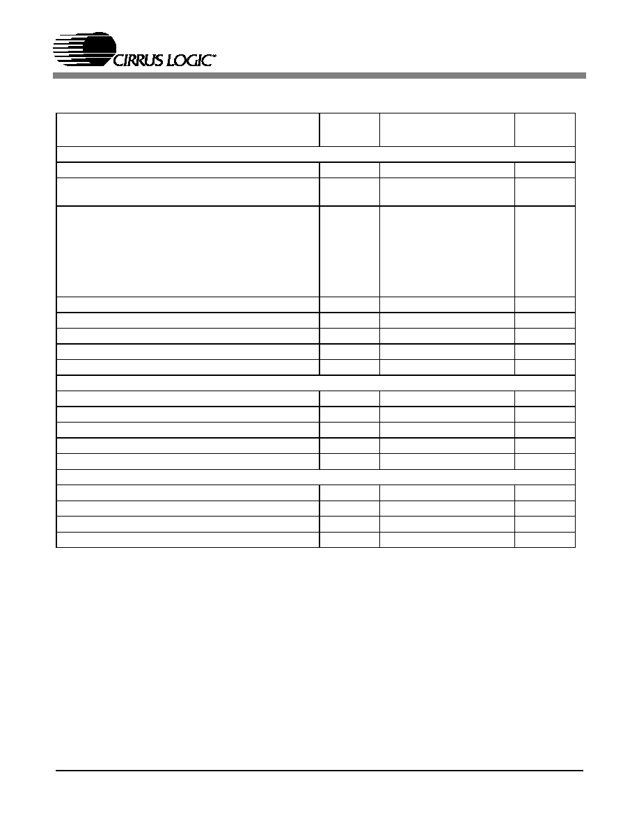
THERMAL CHARACTERISTICS
ANALOG CHARACTERISTICS
Notes: 4. Guaranteed by design and/or characterization.
5. Tested with a full scale input signal of 31.25 Hz.
6. Noise in the harmonic bins dominates THD and linearity measurements for x16, x32, and x64 gains.
Parameter
Symbol
CS3302
Unit
Min
Typ
Max
Allowable Junction Temperature
-
-
135
∫C
Junction to Ambient Thermal Impedance
JA
-
65
-
∫C / W
Ambient Operating Temperature (Power Applied)
T
A
-40
-
+85
∫C
Parameter
Symbol
CS3302
Unit
Min
Typ
Max
Noise Performance, Normal Power
Input Voltage Noise
f
0
= 0.1 Hz to 10 Hz
VN
PP
-
1
1.5
µ
V
p-p
Input Voltage Noise Density
f
0
= 200 Hz to 2 kHz
VN
D
-
8.5
12
Input Current Noise Density
(
Note 4
)
IN
D
-
1
-
Noise Performance, Low Power (LPWR=1)
Input Voltage Noise
f
0
= 0.1 Hz to 10 Hz
VN
PP
-
1
1.5
µ
V
p-p
Input Voltage Noise Density
f
0
= 200 Hz to 2 kHz
VN
D
-
10
15
Input Current Noise Density
(
Note 4
)
IN
D
-
1
-
Distortion Performance, Normal Power
Total Harmonic Distortion
(
Note 5
,
6
)
THD
-
-118
-112
dB
Linearity
(
Note 5
,
6
)
LIN
-
0.000126
0.000251
%
Distortion Performance, Low Power (LPWR=1)
Total Harmonic Distortion
(
Note 5
,
6
)
THD
-
-118
-110
dB
Linearity
(
Note 5
,
6
)
LIN
-
0.000126
0.000316
%
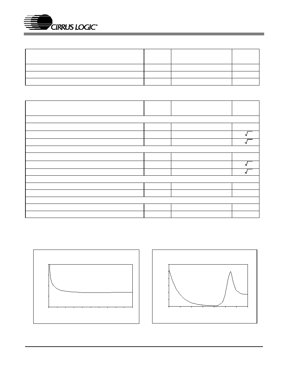
nV/ Hz
fA/ Hz
nV/ Hz
fA/ Hz
CS3302 In-Band Noise
0
5
10
15
20
0
200
400
600
800 1000 1200 1400 1600 1800 2000
Fre quency (Hz)
Noi
s
e
De
n
s
i
t
y
(
n
V
/
r
t
Hz
)
CS3302 Wide Band Noise
0
50
100
150
200
250
300
0.1
1
10
100
1000
10000 100000 1E+06
Fre que ncy (Hz)
Noi
s
e
De
ns
i
t
y
(
n
V
/
r
t
Hz)
Figure 1. CS3302 Noise Performance
CS3302
6
ANALOG CHARACTERISTICS (CONT.)
Notes: 7. Absolute gain accuracy tests the matching of x1 gain across multiple CS3302 devices.
8. Relative gain accuracy tests the tracking of x2 - x64 gain relative to x1 gain on a single CS3302 device.
9. Specification is for the parameter over the specified temperature range and is for the CS3302 device
only. It does not include the effects of external components.
10. Offset voltage is tested with the amplifier inputs connected to the internal 800
termination.
11. The absolute offset after calibration specification applies to the effective offset voltage of the CS3302
output when used with the CS5371/72 modulator and CS5376A digital filter, and is measured from the
digitally calibrated output codes of the CS5376A.
12. The CS3302 offset calibration is performed digitally with the CS5371/72 modulator and CS5376A digital
filter and includes the full scale signal range. Calibration offsets of greater than + 5% of full scale will
begin to subtract from system dynamic range.
Parameter
Symbol
CS3302
Unit
Min
Typ
Max
Gain
Gain, Differential
GAIN
DM
x1
-
x64
Gain, Common Mode
GAIN
CM
-
x1
-
Gain Accuracy, Absolute
(
Note 7
,
9
)
GA
ABS
-
+1
+2
%
Gain Accuracy, Relative
(
Note 8
,
9
)
GA
REL
-
+0.4
+0.8
%
Gain Drift
(
Note 4)
GAIN
TC
-
5
-
ppm / ∫C
Offset
Offset Voltage, Input Referred
(
Note 9
,
10
)
OFST
-
+250
+750
µV
Offset After Calibration, Absolute
(
Note 11
)
OFST
CAL
-
+1
-
µV
Offset Calibration Range
(
Note 12
) OFST
RNG
-
100
-
% F.S.
Offset Voltage Drift
(
Note 4
)
OFST
TC
-
1
-
µV / ∫C
CS3302
7
ANALOG CHARACTERISTIC (Cont.)
Notes: 13. No signal sources operating from external supplies should be applied to pins of the device prior to its
own supplies being established. Connecting any terminal to voltages greater than VA+ or less than VA-
may cause destructive latch-up.
14. Common-to-differential mode rejection tested with a 50 Hz, 500 mVp-p common mode sine wave
applied to the analog inputs.
15. Output impedance is primarily determined by the integrated anti-alias resistors. Value is approximate
and can vary +/- 30% depending on process parameters.
Parameter
Symbol
CS3302
Unit
Min
Typ
Max
Analog Input Characteristics
Input Signal Frequencies
BW
DC
-
2000
Hz
Input Voltage Range (Signal + Vcm)
x1
(
Note 13
)
x2 - x64
V
IN
(VA-)+0.7
(VA-)+0.7
-
-
(VA+)-1.25
(VA+)-1.75
V
Full Scale Input, Differential
x1
x2
x4
x8
x16
x32
x64
V
INFS
-
-
-
-
-
-
-
-
-
-
-
-
-
-
5
2.5
1.25
625
312.5
156.25
78.125
V
p-p
V
p-p
V
p-p
mV
p-p
mV
p-p
mV
p-p
mV
p-p
Input Impedance, Differential
Z
INDIFF
-
1, 20
-
T
, pF
Input Impedance, Common Mode
Z
INCM
-
0.5, 40
-
T
,
pF
Input Bias Current
I
IN
-
1
40
pA
Crosstalk, Multiplexed Inputs
(
Note 4
)
XT
-
-130
-
dB
Common Mode to Differential Mode Rejection (
Note 14
)
CDMR
90
100
-
dB
Analog Output Characteristics
Output Voltage Range (Signal + Vcm)
V
OUT
(VA-)+0.5
-
(VA+)-0.5
V
Full Scale Output, Differential
V
OUTFS
-
-
5
V
p-p
Output Impedance
(
Note 15
)
Z
OUT
-
750
-
Output Current
I
OUT
-
-
3.33
mA
Load Capacitance
C
L
-
-
100
nF
Guard Output Characteristics
Guard Output Voltage
V
GUARD
-
V
cm
-
V
Guard Output Impedance
ZG
OUT
-
500
-
Guard Output Current
IG
OUT
-
40
-
µ
A
Guard Load Capacitance
CG
L
-
-
100
pF
CS3302
8
DIGITAL CHARACTERISTICS
Notes: 16. Device is intended to be driven with CMOS logic levels.
Parameter
Symbol
CS3302
Unit
Min
Typ
Max
Digital Characteristics
High Level Input Drive Voltage
(
Note 16
)
V
IH
0.6*VD
-
VD
V
Low Level Input Drive Voltage
(
Note 16
)
V
IL
0.0
-
0.8
V
Input Leakage Current
I
IN
-
+1
+10
µ
A
Digital Input Capacitance
C
IN
-
9
-
pF
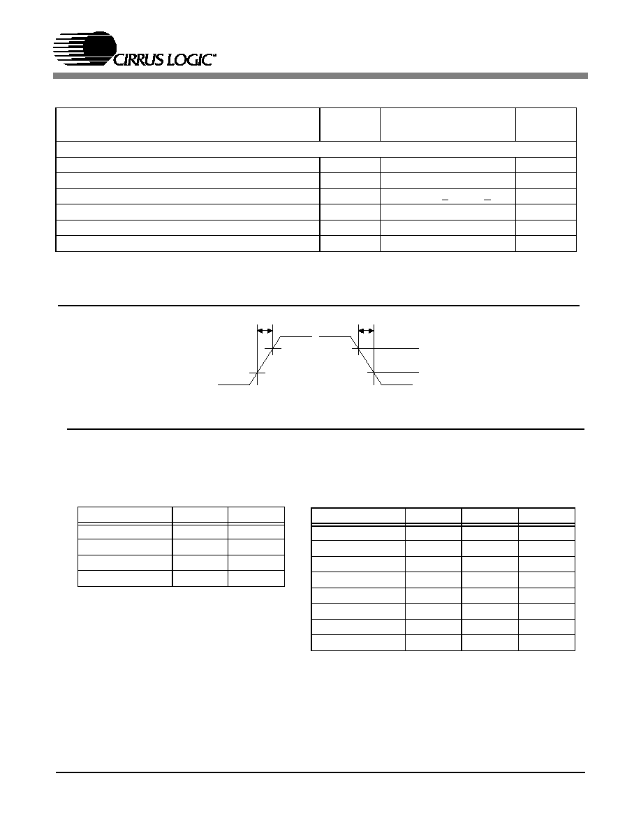
Rise Times
t
RISE
-
-
100
ns
Fall Times
t
FALL
-
-
100
ns
(0.2*VD)
t
fallin
t
risein
(0.8*VD)
Figure 2. Digital Input Rise and Fall
Gain Selection
GAIN2
GAIN1
GAIN0
x1
0
0
0
x2
0
0
1
x4
0
1
0
x8
0
1
1
x16
1
0
0
x32
1
0
1
x64
1
1
0
Reserved
1
1
1
Input Selection
MUX1
MUX0
800
termination
0
0
INA only
1
0
INB only
0
1
INA + INB
1
1
Table 1. Digital Selection for Gain and Input Mux Control
CS3302
9
POWER SUPPLY CHARACTERISTICS
Notes: 17. All outputs unloaded. Analog inputs connected to the internal 800
termination. Digital inputs forced to
VD or DGND respectively.
18. Power supply rejection tested with a 50 Hz, 400 mVp-p sine wave applied separately to each supply.
Parameter
Symbol
CS3302
Unit
Min
Typ
Max
Power Supply Current, Normal Mode
Analog Power Supply Current
(
Note 17
)
I
A
-
5.0
5.75
mA
Digital Power Supply Current
(
Note 17
)
I
D
-
0.1
0.2
mA
Power Supply Current, Low Power Mode
Analog Power Supply Current, LPWR = 1
(
Note 17
)
I
A
-
3.4
4.0
mA
Digital Power Supply Current, LPWR = 1
(
Note 17
)
I
D
-
0.1
0.2
mA
Power Supply Current, Power Down Mode
Analog Power Supply Current, PWDN = 1
(
Note 17
)
I
A
-
9
11
µ
A
Digital Power Supply Current, PWDN = 1
(
Note 17
)
I
D
-
2
8
µ
A
Power Supply Rejection
Power Supply Rejection Ratio
(
Note 18
)
PSRR
95
120
-
dB

CS3302
10
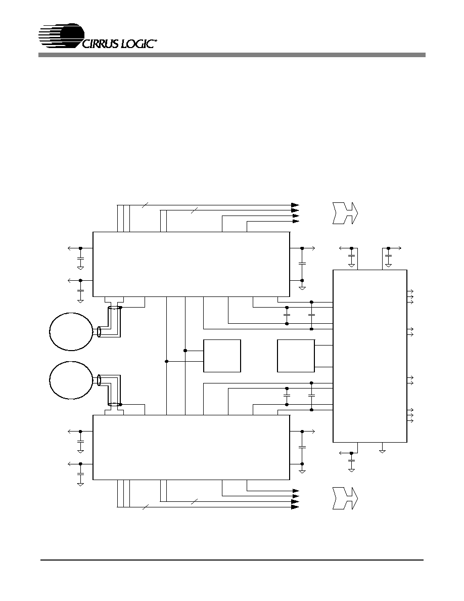
2.
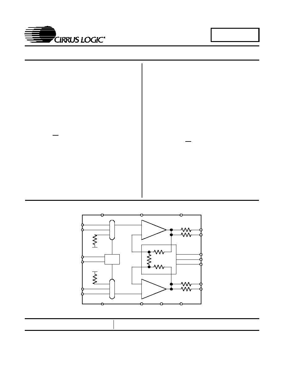
GENERAL DESCRIPTION
The CS3302 is a high impedance low-noise CMOS
differential input, differential output amplifier for
precision analog signals between DC and 2 kHz. It
has multiplexed inputs, rough/fine charge outputs,
and programmable gains of x1, x2, x4, x8, x16,
x32, and x64.
The amplifier's performance makes it ideal for
low-frequency, high dynamic range applications
requiring low distortion and minimal power con-
sumption. It's optimized for use in acquisition sys-
tems designed around the CS5371/72 single/dual
modulators and the CS5376A quad digital fil-
ter.
Figure 3
shows the system level architecture
of a 4-channel acquisition system using four
CS3302, two CS5372, and one CS5376A.
2.1
Analog Signals
2.1.1
Analog Inputs
The amplifier analog inputs are designed for high
impedance differential sensors. Input multiplexing
simplifies system connections by providing sepa-
rate inputs for a sensor and test DAC (INA, INB) as
well as an internal termination for noise tests. The
MUX0, MUX1 digital pins determine which multi-
plexed input is connected to the amplifier.
2.1.2
Analog Outputs
The amplifier analog outputs are separated into
rough charge / fine charge signals to easily connect
to the CS5371/72 inputs. Each output also includes
a series resistor, requiring only two differential ca-
pacitors to create the CS5371/72 input anti-alias
filter.
Differential
Sensor
Differential
Sensor
Differential
Sensor
Differential
Sensor
Modulator
CS5371/72
Modulator
CS5371/72
Digital Filter
CS5376
Test
DAC
µ
Controller
or
Configuration
EEPROM
System
Telemetry
CS89712
EP7312
CS8900A
AMP
M
U
X
CS3302
AMP
M
U
X
CS3302
AMP
M
U
X
CS3302
AMP
M
U
X
CS3302
CS4373
Figure 3. System Architecture
CS5376A

CS3302
11
2.1.3
Differential Signals
Analog signals into and out of the CS3302 are dif-
ferential, consisting of two halves with equal but
opposite magnitude varying about a common mode
voltage.
A full scale 5 Vpp differential signal centered on a
2.5 V common mode can have:
SIG+ = 2.5 V + 1.25 V = 3.75 V
SIG- = 2.5 V - 1.25 V = 1.25 V
SIG+ is +2.5 V relative to SIG-
For the reverse case:
SIG+ = 2.5 V - 1.25 V = 1.25 V
SIG- = 2.5 V + 1.25 V = 3.75 V
SIG+ is -2.5 V relative to SIG-
The total swing for SIG+ relative to SIG- is
(+2.5 V) - (-2.5 V) = 5 Vpp. A similar calculation
can be done for SIG- relative to SIG+. Note that a
5 Vpp differential signal centered on a 2.5 V com-
mon mode voltage never exceeds 3.75 V and never
drops below 1.25 V on either half of the signal.
2.1.4
Guard Output
The GUARD pin outputs the common mode volt-
age of the currently selected analog signal input. It
can be used to drive the cable shield between a high
impedance sensor and the amplifier inputs. Driving
the cable shield with the analog signal common
mode voltage minimizes leakage and improves sig-
nal integrity from high impedance sensors.
The GUARD output is defined as the midpoint
voltage between the + and - halves of the currently
selected differential input signal, and will vary as
the signal common mode varies. The GUARD out-
put will not drive a significant load, it only provides
a shielding voltage.
2.2
Digital Signals
2.2.1
Gain Selection
The CS3302 supports gain ranges of x1, x2, x4, x8,
x16, x32, and x64. They are selected using the
GAIN0, GAIN1, and GAIN2 pins as shown in
Table 1 on page 8
.
2.2.2
Mux Selection
The analog inputs to the amplifier are multiplexed,
with external signals applied to the INA+, INA- or
INB+, INB- pins. An internal termination is also
available for noise tests. Input mux selection is
made using the MUX0 and MUX1 pins as shown in
Table 1 on page 8
.
Although a mux selection is provided to enable the
INA and INB switches simultaneously, significant
current should not be driven through them in this
mode. The CS3302 mux switches will maintain
good linearity only with minimal signal current.
2.2.3
Low Power Selection
For applications where power is critical, a low-
power mode can be selected. This mode reduces
amplifier power consumption at the expense of
slightly degraded performance. Low power mode
is selected using the LPWR pin, which is active
high.
2.2.4
Power Down Selection
A power-down mode is available to shut down the
amplifier when not in use. When enabled, all inter-
nal circuitry is disabled, the analog inputs and out-
puts go high-impedance, and the device enters a
micro-power state. Power down mode is selected
using the PWDN pin, which is active high.
2.3
Power Supplies
2.3.1
Analog Power Supplies
The analog power pins of the CS3302 are to be sup-
plied with a total of 5 V between VA+ and VA-.
This voltage can be from a unipolar +5 V / 0 V sup-
ply or a bipolar +2.5 V / -2.5 V supply. When using
a unipolar supply, analog signal common mode
should be biased to 2.5 V, and when using bipolar
supplies it should be biased to 0 V. The analog
power supplies are recommended to be bypassed to
system ground using 0.1
µ
F X7R type capacitors.

CS3302
12
The VA- supply is connected to the CMOS sub-
strate and as such must remain the most negative
applied voltage to prevent potential latch-up condi-
tions. Care should be taken to ensure analog input
voltages do not drop more than -0.3 V below the
VA- supply. Care should also be taken to establish
the VA- supply before analog signals are applied to
the device. It is recommended to clamp the VA-
supply to system ground using a reverse biased
Schottky diode to prevent possible latch-up condi-
tions related to mismatched supply rail initializa-
tion.
2.3.2
Digital Power Supplies
The digital power supply across the VD and DGND
pins is flexible and can be set to interface with
3.3 V or 5 V logic. The digital power supply should
be bypassed to system ground using a 0.01
µ
F X7R
type capacitor.
CS3302
13
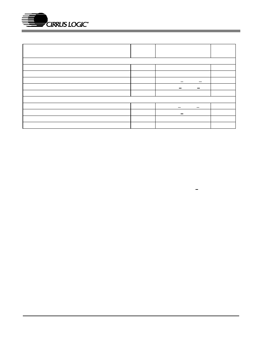
2.4
Connection Diagram
Figure 4
shows a connection diagram for the
CS3302 amplifier when used with the CS5372 dual
modulator and CS5376A digital filter. The dia-
gram shows differential sensors, a test DAC, and
analog outputs with anti-alias capacitors; power
supply connections including recommended by-
passing; and digital control connections back to the
CS5376A GPIO pins.
0 .0 2
µ
F
C 0G
0.0 2
µ
F
C0 G
0 .0 2
µ
F
C 0G
0.0 2
µ
F
C0 G
C S5372
M o du lator
INF +
INR +
INF -
INR -
INF -
INR -
INF +
INR +
V RE F+
V RE F-
VA +
VA -
VD
D GN D
M DA TA 1
M FL A G1
M DA TA 2
M FL A G2
M C LK
M SYN C
PW DN 1
OF ST
PW DN 2
LP W R
C S3302
D ifferential
Am p lifier
IN B +
IN A +
IN A -
IN B -
OU TF -
O UT R -
OU T F+
O UT R+
VA +
VA -
V D
D GN D
GA IN
M U X
P W D N
LPW R
C S3302
D ifferential
Am p lifier
IN B +
IN A +
IN A -
IN B -
OU TF -
O UT R -
OU T F+
O UT R+
V A+
V A-
V D
D GN D
G A IN
M UX
PW D N
LP W R
VA -
0 .1
µ
F
VA +
0 .1
µ
F
VA -
0 .1
µ
F
VA +
0 .1
µ
F
V D
0.0 1
µ
F
V D
0.0 1
µ
F
G PIO
G PIO
G PIO (x2)
G PIO (x3)
G PIO
G PIO
G PIO (x2)
G PIO (x3)
D ifferential
Senso r
D ifferential
Senso r
Test
D A C
3
2
3
2
To CS 5376
D ig ital C on tro l
To CS 5376
D ig ital C on tro l
2.5 V
R eference
VA +
0 .1
µ
F
0 .0 1
µ
F
VD
V A-
0.1
µ
F
G U AR D
GU AR D
Figure 4. CS3302 Amplifier Connections
A
A
CS4373
CS3302
14
3.
PIN DESCRIPTION
Pin Name
Pin #
I/O
Pin Description
VA+
1
I
Positive analog supply voltage.
VA-
4
I
Negative analog supply voltage.
VD
16
I
Positive digital supply voltage.
DGND
15
I
Digital ground.
INA+, INA-
5, 6
I
Channel A differential analog inputs. Selected via MUX pins.
INB+, INB-
8, 7
I
Channel B differential analog inputs. Selected via MUX pins.
GUARD
13
O
Guard voltage output.
OUTR+, OUTR-
11, 2
O
Rough charge differential analog outputs.
OUTF+, OUTF-
10, 3
O
Fine charge differential analog outputs.
GAIN0, GAIN1,
GAIN2
22, 21,
20
I
Gain range select. See Gain Selection table in Digital Characteristics section.
LPWR
18
I
Low power mode enable. Active high.
PWDN
19
I
Power down mode enable. Active high.
MUX0, MUX1
24, 23
I
Analog input select. See Input Selection table in Digital Characteristics section.
TEST0
12
I
Test mode select, factory use only. Connect to VA- during normal operation.
TEST1, TEST2
17, 14
I
Test mode select, factory use only. Connect to DGND during normal operation.
TESTOUT
9
O
Test mode output, factory use only. Connect to VA- during normal operation.
Table 2. Pin Descriptions
1
2
3
4
5
6
7
8
17
18
19
20
21
22
23
24
9
10
11
12
13
14
15
16
Positive Analog Power Supply
VA+
Negative Analog Rough Output
OUTR-
Negative Analog Fine Output
OUTF-
Negative Analog Power Supply
VA-
Non-Inverting Input A
INA+
Inverting Input A
INA-
Inverting Input B
INB-
Non-Inverting Input B
INB+
Test Mode Output
TESTOUT
Positive Analog Fine Output
OUTF+
Positive Analog Rough Output
OUTR+
Test Mode Select
TEST0
MUX0
Input Mux Select
MUX1
Input Mux Select
GAIN0
Gain Range Select
GAIN1
Gain Range Select
GAIN2
Gain Range Select
PWDN
Power Down Mode Enable
LPWR
Low Power Mode Enable
TEST1
Test Mode Select
VD
Positive Digital Power Supply
DGND
Digital Ground
TEST2
Test Mode Select
GUARD
Guard Voltage Output
Figure 5. CS3302 Pin Assignments

CS3302
15
4.
PACKAGE DIMENSIONS
Notes: 1. "D" and "E1" are reference datums and do not included mold flash or protrusions, but do include mold
mismatch and are measured at the parting line, mold flash or protrusions shall not exceed 0.20 mm per
side.
2. Dimension "b" does not include dambar protrusion/intrusion. Allowable dambar protrusion shall be
0.13 mm total in excess of "b" dimension at maximum material condition. Dambar intrusion shall not
reduce dimension "b" by more than 0.07 mm at least material condition.
3. These dimensions apply to the flat section of the lead between 0.10 and 0.25 mm from lead tips.
INCHES
MILLIMETERS
NOTE
DIM
MIN
MAX
MIN
MAX
A
--
0.084
--
2.13
A1
0.002
0.010
0.05
0.25
A2
0.064
0.074
1.62
1.88
b
0.009
0.015
0.22
0.38
2,3
D
0.311
0.335
7.90
8.50
1
E
0.291
0.323
7.40
8.20
E1
0.197
0.220
5.00
5.60
1
e
0.024
0.027
0.61
0.69
L
0.025
0.040
0.63
1.03
0∞
8∞
0∞
8∞
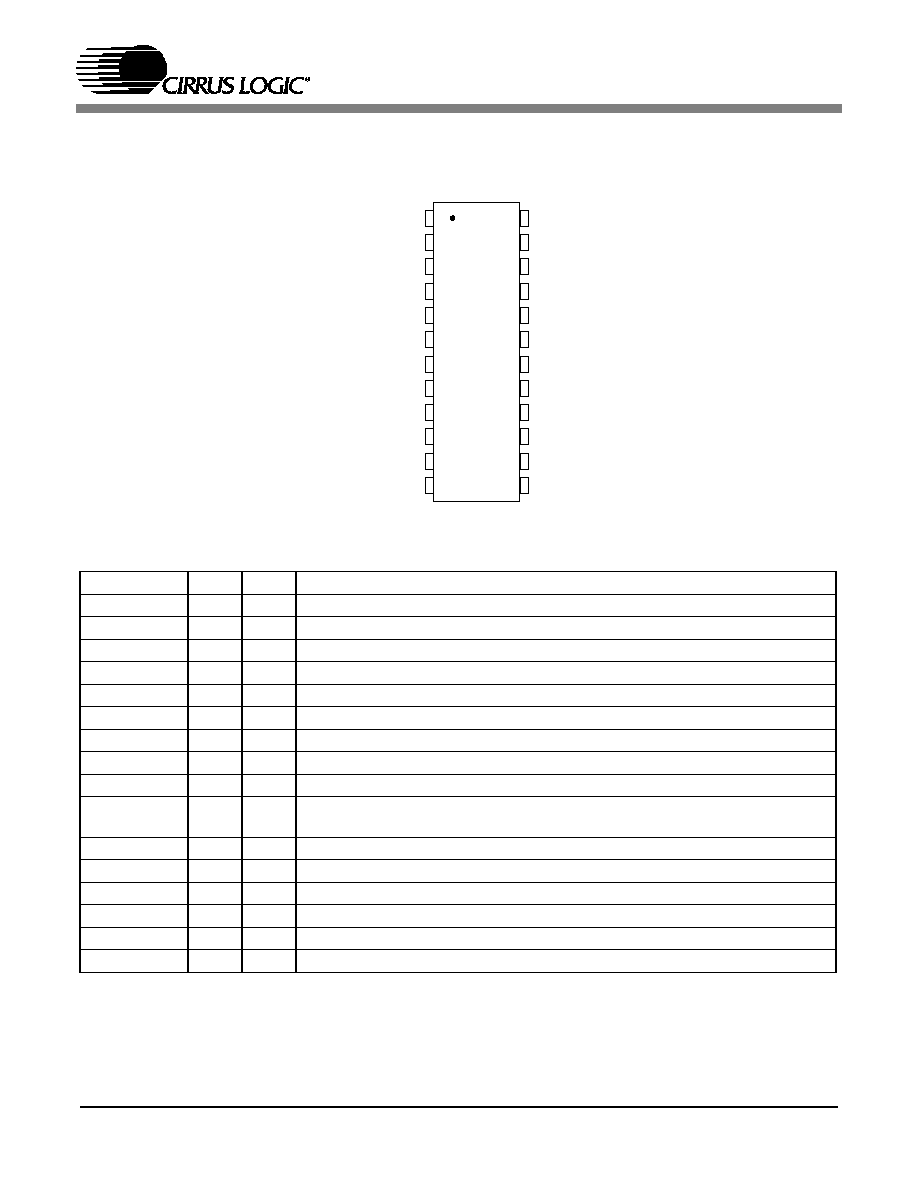
24 PIN SSOP PACKAGE DRAWING
E
N
1 2 3
e
b
2
A1
A2
A
D
SEATING
PLANE
E1
1
L
SIDE VIEW
END VIEW
TOP VIEW