| –≠–ª–µ–∫—Ç—Ä–æ–Ω–Ω—ã–π –∫–æ–º–ø–æ–Ω–µ–Ω—Ç: CS4205-KQ | –°–∫–∞—á–∞—Ç—å:  PDF PDF  ZIP ZIP |
Preliminary Product Information
This document contains information for a new product.
Cirrus Logic reserves the right to modify this product without notice.
1
Copyright
Cirrus Logic, Inc. 2001
(All Rights Reserved)
P.O. Box 17847, Austin, Texas 78760
(512) 445 7222 FAX: (512) 445 7581
http://www.cirrus.com
CS4205
CrystalClear
Audio Codec '97 for Portable Computing
Features
l
Integrated Asynchronous I
2
S Input Port
(ZV Port)
l
Integrated High-Performance Microphone
Pre-Amplifier
l
Integrated Digital Effects Processing for Bass
and Treble Response
l
Digital Docking Including an I
2
S Output, 3
Synchronous I
2
S Inputs
l
Performance Oriented Digital Mixer
l
SRS
3D Stereo Enhancement
l
On-chip PLL for use with External Clock
Sources
l
Dedicated Microphone Analog-to-Digital
Converter
l
Sample Rate Converters
l
S/PDIF Digital Audio Output
l
AC '97 2.1 Compliant
l
PC Beep Bypass
l
20-bit Stereo Digital-to-Analog Converters
l
18-bit Stereo Analog-to-Digital Converters
l
Three Analog Line-level Stereo Inputs for
LINE IN, VIDEO, and AUX
l
High Quality Pseudo-Differential CD Input
l
Extensive Power Management Support
l
Meets or Exceeds the Microsoft
PC 99 and
PC 2001 Audio Performance Requirements
Description
The CS4205 is an AC '97 2.1 compliant stereo audio co-
dec designed for PC multimedia systems. It uses
industry leading CrystalClear
delta-sigma and mixed
signal technology. The CS405 is the first Cirrus AC '97
audio codec to feature digital centric mixing and digital
effects. This advanced technology and these features
are designed to help enable the design of PC 99 and
PC 2001 compliant high-quality audio systems for desk-
top, portable, and entertainment PCs.
Coupling the CS4205 with a PCI audio accelerator or
core logic supporting the AC '97 interface, implements a
cost effective, superior quality audio solution. The
CS4205 surpasses PC 99, PC 2001, and AC '97 2.1 au-
dio quality standards.
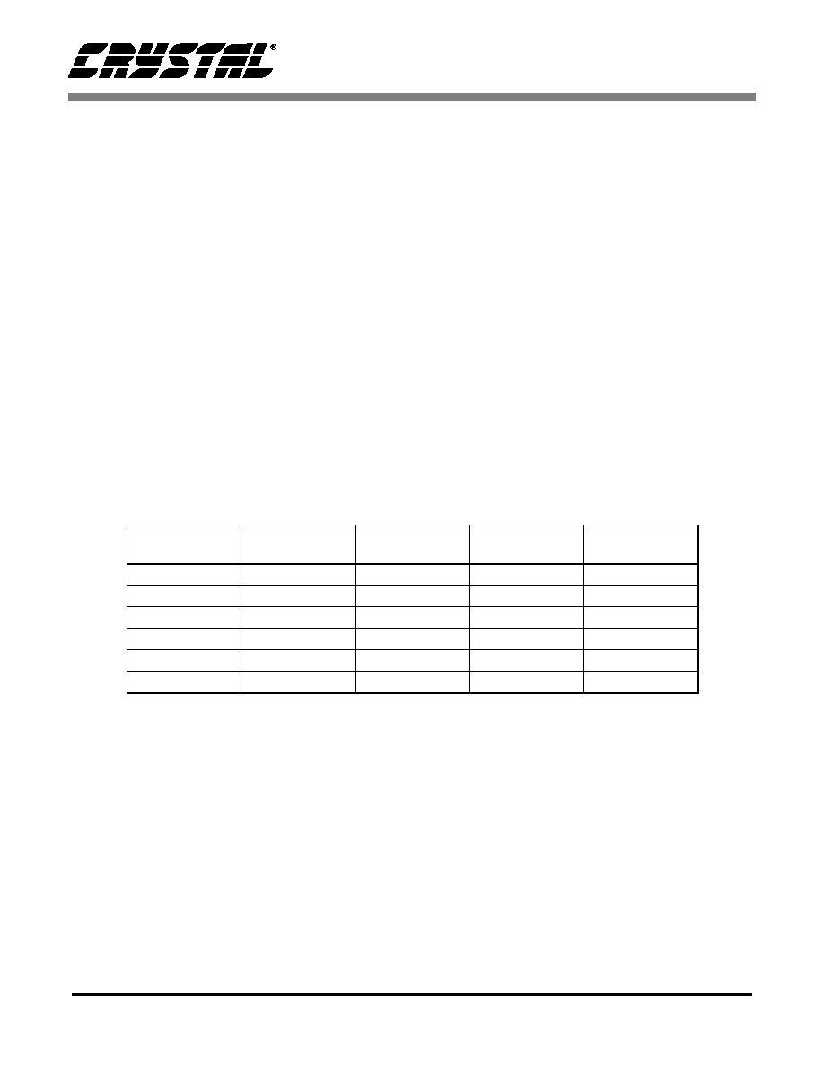
ORDERING INFO
CS4205-KQ
48-pin TQFP
9x9x1.4 mm
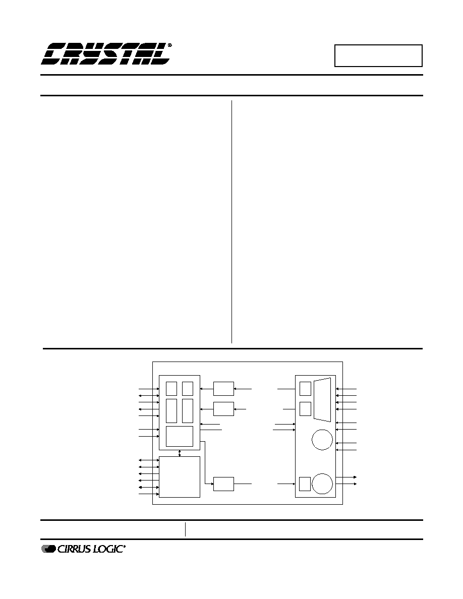
SIGNAL
PROCESSING
ENGINE
LINE
CD
AUX
VIDEO
MIC1
MIC2
PHONE
PC_BEEP
LINE_OUT
MONO_OUT
ANALOG INPUT MUX
AND OUTPUT MIXER
AC-LINK AND AC '97
REGISTERS
PCM_DATA
GAIN / MUTE CONTROLS
INPUT
MUX
OUTPUT
MIXER
MIXER / MUX SELECTS
AC-
LINK
PWR
MGT
TEST
SYNC
BIT_CLK
SDATA_OUT
SDATA_IN
RESET#
PCM_DATA
SRC
SRC
ID0#
ID1#
GPIO
S/PDIF
SERIAL DATA PORT
ZV PORT
GPIO0/LRCLK
GPIO1/SDOUT
EAPD/SCLK
SPDO/SDO2
18 bit
ADC
(2ch)
20 bit
DAC
(2ch)
INPUT
MIXER
AC
'97
REG
GPIO[2:4]/SDI[1:3]
ZSCLK,ZSDATA,ZLRCLK
18 bit
ADC
(1ch)
SRC
MIC_PCM_DATA
APR `01
DS489PP2

CS4205
2
DS489PP2
TABLE OF CONTENTS
1. CHARACTERISTICS AND SPECIFICATIONS ..................................................................7
Analog Characteristics ........................................................................................................7
Absolute Maximum Ratings ................................................................................................8
Recommended Operating Conditions.................................................................................8
AC '97 Serial Port Timing..................................................................................................10
2. GENERAL DESCRIPTION ...............................................................................................13
2.1 AC-Link ......................................................................................................................13
2.2 Control Registers .......................................................................................................14
2.3 Sample Rate Converters ...........................................................................................14
2.4 Mixers ........................................................................................................................14
2.5 Input Mux ...................................................................................................................14
2.6 Volume Control ..........................................................................................................14
2.7 Dedicated Mic Record Path .......................................................................................14
3. DIGITAL SIGNAL PATHS ................................................................................................16
3.1 Analog Centric Mode .................................................................................................16
3.2 Digital Centric Mode ..................................................................................................17
3.3 Host Processing Mode ..............................................................................................17
3.4 Multi-Channel Mode ..................................................................................................17
4. AC-LINK FRAME DEFINITION ........................................................................................19
4.1 AC-Link Serial Data Output Frame ............................................................................20
4.1.1 Serial Data Output Slot Tags (Slot 0) ...........................................................20
4.1.2 Command Address Port (Slot 1) ..................................................................20
4.1.3 Command Data Port (Slot 2) ........................................................................21
4.1.4 PCM Playback Data (Slots 3-11) .................................................................21
4.1.5 GPIO Pin Control (Slot12) ............................................................................21
4.2 AC-Link Serial Data Input Frame ..............................................................................22
4.2.1 Serial Data Input Slot Tag Bits (Slot 0) ......................................................22
4.2.2 Status Address Port (Slot 1) .........................................................................22
4.2.3 Status Data Port (Slot 2) ..............................................................................23
4.2.4 PCM Capture Data (Slot 3-8) .......................................................................23
4.2.5 GPIO Pin Status (Slot 12) ...........................................................................23
4.3 AC-Link Protocol Violation - Loss of SYNC ...............................................................24
5. REGISTER INTERFACE .............................................................................................25
5.1 Reset Register (Index 00h) ......................................................................................27
5.2 Master Volume Register (Index 02h) .......................................................................27
Contacting Cirrus Logic Support
For a complete listing of Direct Sales, Distributor, and Sales Representative contacts, visit the Cirrus Logic web site at:
http://www.cirrus.com/corporate/contacts/sales.cfm
Microsoft is a registered trademark of Microsoft Corporation in the United States and/or other countries.
Intel is a registered trademark of Intel Corporation.
CrystalClear is a registered trademark of Cirrus Logic.
Preliminary product information describes products which are in production, but for which full characterization data is not yet available. Advance product infor-
mation describes products which are in development and subject to development changes. Cirrus Logic, Inc. has made best efforts to ensure that the information
contained in this document is accurate and reliable. However, the information is subject to change without notice and is provided "AS IS" without warranty of any
kind (express or implied). No responsibility is assumed by Cirrus Logic, Inc. for the use of this information, nor for infringements of patents or other rights of third
parties. This document is the property of Cirrus Logic, Inc. and implies no license under patents, copyrights, trademarks, or trade secrets. No part of this publi-
cation may be copied, reproduced, stored in a retrieval system, or transmitted, in any form or by any means (electronic, mechanical, photographic, or otherwise)
without the prior written consent of Cirrus Logic, Inc. Items from any Cirrus Logic website or disk may be printed for use by the user. However, no part of the
printout or electronic files may be copied, reproduced, stored in a retrieval system, or transmitted, in any form or by any means (electronic, mechanical, photo-
graphic, or otherwise) without the prior written consent of Cirrus Logic, Inc.Furthermore, no part of this publication may be used as a basis for manufacture or
sale of any items without the prior written consent of Cirrus Logic, Inc. The names of products of Cirrus Logic, Inc. or other vendors and suppliers appearing in
this document may be trademarks or service marks of their respective owners which may be registered in some jurisdictions. A list of Cirrus Logic, Inc. trade-
marks and service marks can be found at http://www.cirrus.com.

CS4205
DS489PP2
3
5.3 Mono Volume Register (Index 06h) .......................................................................... 28
5.4 Master Tone Control Register (Index 08h) ............................................................... 28
5.5 PC_BEEP Volume Register (Index 0Ah) .................................................................. 29
5.6 Phone Volume Register (Index 0Ch) ........................................................................ 29
5.7 Microphone Volume Register (Index 0Eh) ................................................................ 30
5.8 Analog Mixer Input Gain Registers (Index 10h - 18h) .............................................. 31
5.9 Input Mux Select Register (Index 1Ah) ..................................................................... 32
5.10 Record Gain Register (Index 1Ch) ......................................................................... 33
5.11 Record Gain Mic Register (Index 1Eh) ................................................................... 33
5.12 General Purpose Register (Index 20h) ................................................................. 34
5.13 3D Control Register (Index 22h) ............................................................................. 34
5.14 Powerdown Control/Status Register (Index 26h) ................................................... 35
5.15 Extended Audio ID Register (Index 28h) ................................................................ 36
5.16 Extended Audio Status/Control Register (Index 2Ah) ............................................ 36
5.17 Audio Sample Rate Control Registers (Index 2Ch - 34h) ....................................... 37
5.18 Extended Modem ID Register (Index 3Ch) ............................................................ 38
5.19 Extended Modem Status/Control Register (Index 3Eh) ......................................... 38
5.20 GPIO Pin Configuration Register (Index 4Ch) ........................................................ 38
5.21 GPIO Pin Polarity/Type Configuration Register (Index 4Eh) .................................. 39
5.22 GPIO Pin Sticky Register (Index 50h) .................................................................... 39
5.23 GPIO Pin Wakeup Mask Register (Index 52h) ...................................................... 40
5.24 GPIO Pin Status Register (Index 54h) ................................................................... 40
5.25 AC Mode Control Register (Index 5Eh) .................................................................. 41
5.26 Misc. Crystal Control Register (Index 60h) ............................................................. 43
5.27 S/PDIF Control Register (Index 68h) ...................................................................... 44
5.28 Serial Port Control Register (Index 6Ah) ................................................................ 45
5.29 Special Feature Address Register (Index 6Ch) ...................................................... 46
5.30 Special Feature Data Register (Index 6Eh) ........................................................... 46
5.31 Digital Mixer Input Volume Registers (Index 6Eh, Address 00h - 05h) .................. 46
5.32 Serial Data Port Volume Control Registers (Index 6Eh, Address 06h - 07h) ......... 47
5.33 Signal Processing Engine Control Register (Index 6Eh, Address 08h) .................. 48
5.34 Internal Error Condition Control/Status Registers (Index 6Eh, Address 09h - 0Bh) 49
5.35 BIOS-Driver Interface Control Registers (Index 6Eh, Address 0Ch - 0Dh) ............ 50
5.36 ZV Port Control/Status Registers (Index 6Eh, Address 0Eh - 0Fh) ........................ 50
5.37 BIOS-Driver Interface Status Register (Index 7Ah) ................................................ 51
5.38 Vendor ID1 Register (Index 7Ch) ........................................................................... 52
5.39 Vendor ID2 Register (Index 7Eh) ........................................................................... 52
6. SERIAL DATA PORTS ..................................................................................................... 53
6.1 Overview ................................................................................................................... 53
6.2 Multi-Channel Expansion .......................................................................................... 53
6.3 Digital Docking .......................................................................................................... 54
6.4 Serial Data Formats .................................................................................................. 54
7. ZV PORT ........................................................................................................................... 56
8. SONY/PHILIPS DIGITAL INTERFACE (S/PDIF) ............................................................. 57
9. EXCLUSIVE FUNCTIONS ................................................................................................ 58
10. POWER MANAGEMENT ............................................................................................... 59
10.1AC '97 Reset Modes ................................................................................................. 59
10.1.1 Cold Reset ................................................................................................. 59
10.1.2 Warm Reset ............................................................................................... 59
10.1.3 New Warm Reset ....................................................................................... 59
10.1.4 Register Reset ........................................................................................... 59
10.2Powerdown Controls ................................................................................................ 60

CS4205
4
DS489PP2
11. CLOCKING .....................................................................................................................62
11.1PLL Operation (External Clock) ................................................................................62
11.224.576 MHz Crystal Operation ..................................................................................62
11.3Secondary Codec Operation .....................................................................................62
12. ANALOG HARDWARE DESCRIPTION .........................................................................64
12.1Analog Inputs ............................................................................................................64
12.1.1 Line Inputs ..................................................................................................64
12.1.2 CD Input .....................................................................................................64
12.1.3 Microphone Inputs ......................................................................................65
12.1.4 PC Beep Input ............................................................................................65
12.1.5 Phone Input ................................................................................................65
12.2Analog Outputs .........................................................................................................65
12.2.1 Stereo Output .............................................................................................66
12.2.2 Mono Output ..............................................................................................66
12.3Miscellaneous Analog Signals ..................................................................................66
12.4Power Supplies .........................................................................................................66
12.5Reference Design .....................................................................................................66
13. GROUNDING AND LAYOUT ........................................................................................67
14. PIN DESCRIPTIONS ..................................................................................................69
Audio I/O Pins .................................................................................................................70
Analog Reference, Filter, and Configuration Pins ...........................................................71
AC-Link Pins ...................................................................................................................72
Clock and Configuration Pins ..........................................................................................72
Misc. Digital Interface Pins ..............................................................................................73
Power Supply Pins ..........................................................................................................74
15. PARAMETER AND TERM DEFINITIONS ......................................................................75
16. REFERENCE DESIGN ..................................................................................................77
17. REFERENCES ................................................................................................................78
18. PACKAGE DIMENSIONS ...............................................................................................79

CS4205
DS489PP2
5
LIST OF FIGURES
Figure 1. Power Up Timing ............................................................................................... 11
Figure 2. Codec Ready from Start-up or Fault Condition ................................................. 11
Figure 3. Clocks................................................................................................................ 11
Figure 4. Data Setup and Hold ......................................................................................... 12
Figure 5. PR4 Powerdown and Warm Reset.................................................................... 12
Figure 6. Test Mode ......................................................................................................... 12
Figure 7. AC-link Connections .......................................................................................... 13
Figure 8. CS4205 Mixer Diagram ..................................................................................... 15
Figure 9. Digital Signal Path Overview ............................................................................. 16
Figure 10. Analog Centric Mode ....................................................................................... 18
Figure 11. Digital Centric Mode ........................................................................................ 18
Figure 12. Host Processing Mode .................................................................................... 18
Figure 13. Multi-Channel Mode ........................................................................................ 18
Figure 14. AC-link Input and Output Framing ................................................................... 19
Figure 15. Serial Data Port: Six Channel Circuit .............................................................. 53
Figure 16. Digital Docking Connection Diagram............................................................... 54
Figure 17. Serial Data Format 0 (I2S) .............................................................................. 55
Figure 18. Serial Data Format 1 (Left Justified)................................................................ 55
Figure 19. Serial Data Format 2 (Right Justified, 20-bit data) .......................................... 55
Figure 20. Serial Data Format 3 (Right Justified, 16-bit data) .......................................... 55
Figure 21. ZV Port Format (I2S, 16-bit data) .................................................................... 56
Figure 22. S/PDIF Output ................................................................................................. 57
Figure 23. PLL External Loop Filter .................................................................................. 62
Figure 24. External Crystal ............................................................................................... 62
Figure 25. Line Input (Replicate for Video and AUX) ....................................................... 64
Figure 26. Differential 2 VRMS CD Input.......................................................................... 64
Figure 27. Differential 1 VRMS CD Input.......................................................................... 64
Figure 28. Microphone Input............................................................................................. 65
Figure 29. PC_BEEP Input ............................................................................................... 65
Figure 30. Modem Connection ......................................................................................... 65
Figure 31. Stereo Output .................................................................................................. 66
Figure 32. +5V Analog Voltage Regulator ........................................................................ 66
Figure 33. Conceptual Layout for the CS4205 when in XTAL or OSC Clocking Modes .. 68
Figure 34. Pin Locations for the CS4205.......................................................................... 69
Figure 35. CS4205 Reference Design.............................................................................. 77

CS4205
6
DS489PP2
LIST OF TABLES
Table 1. AC Mode Control Configurations ........................................................................17
Table 2. Register Overview for the CS4205 .....................................................................25
Table 3. Indirectly Addressed Register Overview .............................................................26
Table 4. Analog Mixer Output Attenuation ........................................................................27
Table 5. Tone Control Values ...........................................................................................28
Table 6. Microphone Input Gain Values............................................................................30
Table 7. Analog Mixer Input Gain Values .........................................................................31
Table 8. Analog Mixer Input Gain Register Index .............................................................31
Table 9. Input Mux Selection ............................................................................................32
Table 10. Record Gain Values..........................................................................................33
Table 11. Audio Sample Rate Control Register Index ......................................................37
Table 12. Directly Supported SRC Sample Rates for the CS4205 ...................................37
Table 13. GPIO Input/Output Configurations ....................................................................39
Table 14. Slot Mapping for the CS4205...........................................................................42
Table 15. Digital Signal Source Selects............................................................................42
Table 16. Serial Data Format Selection ............................................................................45
Table 17. Digital Mixer Input Volume Register Index........................................................46
Table 18. Serial Port Volume Control Register Index .......................................................47
Table 19. Volume Change Modes and EQ Filter Selects .................................................48
Table 20. Internal Error Sources and Correction Methods ...............................................49
Table 21. ZV Port Control/Status Register Index..............................................................50
Table 22. Device ID with Corresponding Part Number .....................................................52
Table 23. Serial Data Formats and Compatible DACs/ADC's for the CS4205 ................55
Table 24. Powerdown PR Bit Functions ...........................................................................60
Table 25. Powerdown PR Function Matrix for the CS4205 ..............................................61
Table 26. Power Consumption by Powerdown Mode for the CS4205..............................61
Table 27. Clocking Configurations for the CS4205...........................................................63
CS4205
DS489PP2
7
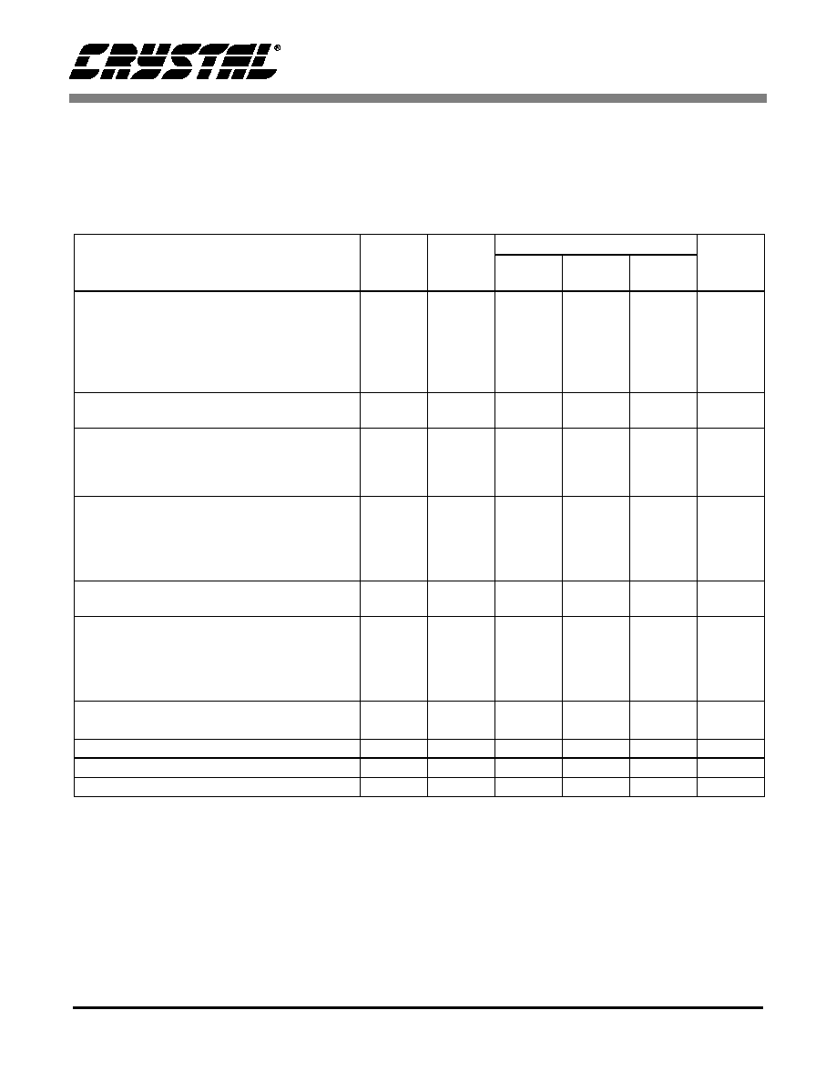
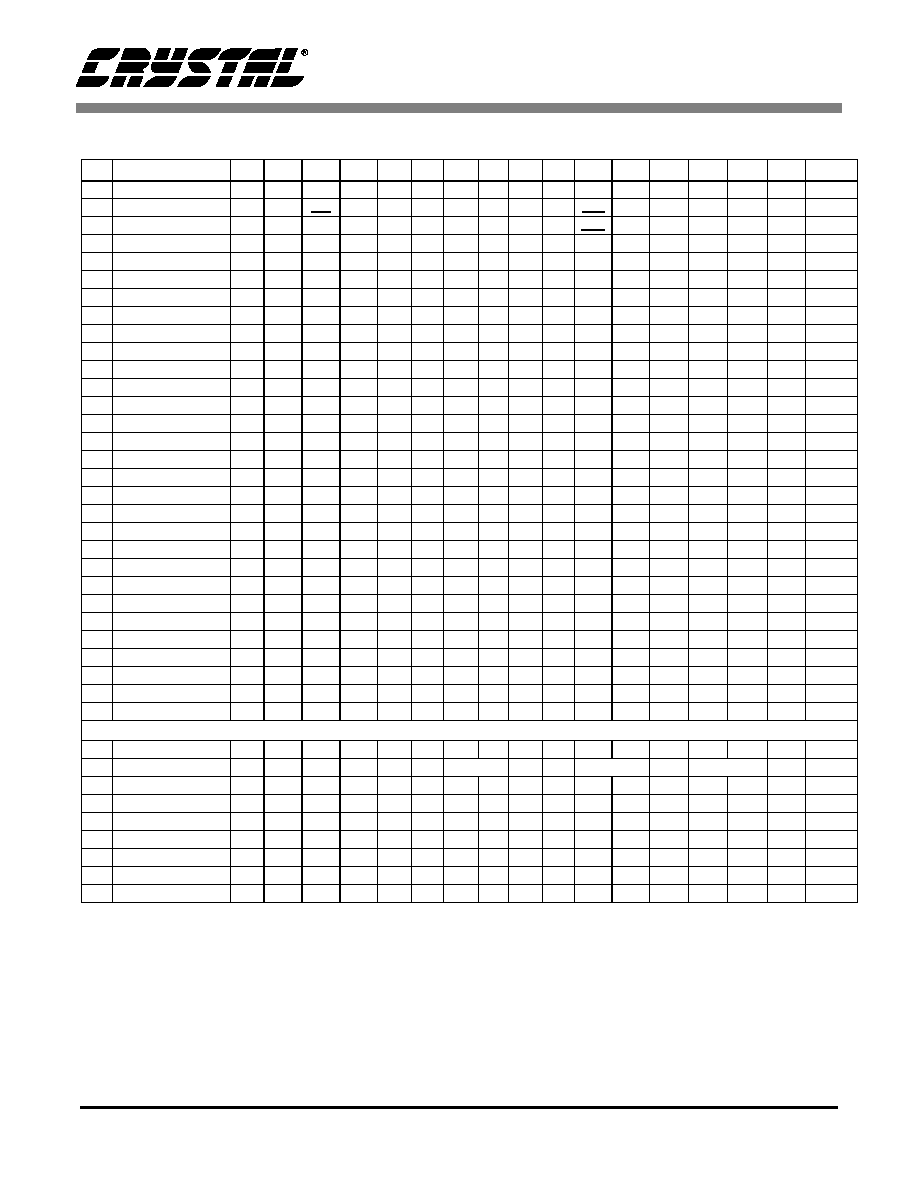
1. CHARACTERISTICS AND SPECIFICATIONS
ANALOG CHARACTERISTICS
(Standard test conditions unless otherwise noted: T
ambient
= 25∞ C,
AVdd = 5.0 V ±5%, DVdd = 3.3 V ±5%; 1 kHz Input Sine wave; Sample Frequency, Fs = 48 kHz; Z
AL
=100 k
/
1000 pF load for Mono and Line Outputs; C
DL
= 18 pF load (Note 1); Measurement bandwidth is 20 Hz - 20 kHz,
18-bit linear coding for ADC functions, 20-bit linear coding for DAC functions; Mixer registers set for unity gain.
Notes: 1. Z
AL
refers to the analog output pin loading and C
DL
refers to the digital output pin loading.
2. Parameter definitions are given in Section 15, Parameter and Term Definitions.
3. Path refers to the signal path used to generate this data. These paths are defined in Section 15,
Parameter and Term Definitions.
4. This specification is guaranteed by silicon characterization; it is not production tested.
Parameter
(Note 2)
Symbol
Path
(Note 3)
CS4205-KQ
Unit
Min Typ
Max
Full Scale Input Voltage
Line Inputs
Mic Inputs
(10dB = 0, 20dB = 0)
Mic Inputs
(10dB = 1, 20dB = 0)
Mic Inputs
(10dB = 0, 20dB = 1)
Mic Inputs
(10dB = 1, 20dB = 1)
A-D
A-D
A-D
A-D
A-D
0.91
0.91
0.283
0.091
0.0283
1.00
1.00
0.315
0.10
0.0315
-
-
-
-
-
V
RMS
V
RMS
V
RMS
V
RMS
V
RMS
Full Scale Output Voltage
Line and Mono Outputs
D-A
0.91
1.0
1.13
V
RMS
Frequency Response
(Note 4)
Analog
Ac = ± 0.5 dB
DAC
Ac = ± 0.5 dB
ADC
Ac = ± 0.5 dB
FR
A-A
D-A
A-D
20
20
20
-
-
-
20,000
20,000
20,000
Hz
Hz
Hz
Dynamic Range
Stereo Analog Inputs to LINE_OUT
Mono Analog Input to LINE_OUT
DAC Dynamic Range
ADC Dynamic Range
DR
A-A
A-A
D-A
A-D
90
85
85
85
95
90
90
90
-
-
-
-
dB FS A
dB FS A
dB FS A
dB FS A
DAC SNR
(-20 dB FS input w/ CCIR-RMS filter on output)
SNR
D-A
-
70
-
dB
Total Harmonic Distortion + Noise
(-3 dB FS input signal):
Line Output
DAC
ADC
(all inputs)
THD+N
A-A
D-A
A-D
-
-
-
-90
-87
-84
-80
-80
-80
dB FS
dB FS
dB FS
Power Supply Rejection Ratio
(1 kHz, 0.5 V
RMS
w/ 5 V DC offset)
(Note 4)
40
60
-
dB
Interchannel Isolation
70
87
-
dB
Spurious Tone
(Note 4)
-
-100
-
dB FS
Input Impedance
(Note 4)
10
-
-
k
CS4205
8
DS489PP2
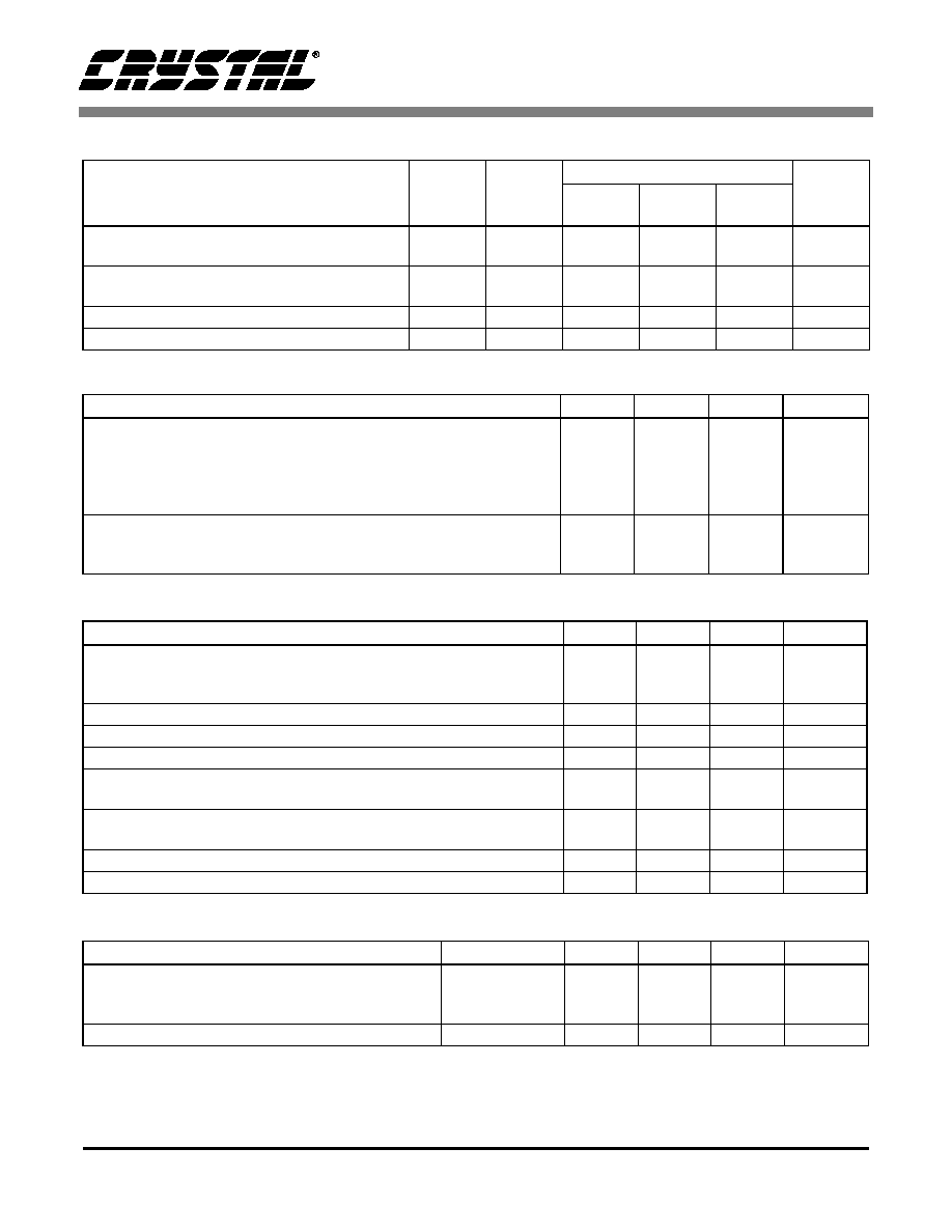
ANALOG CHARACTERISTICS
(Continued)
MIXER CHARACTERISTICS
ABSOLUTE MAXIMUM RATINGS
(AVss1 = AVss2 = DVss1 = DVss2 = 0 V)
RECOMMENDED OPERATING CONDITIONS
(AVss1 = AVss2 = DVss1 = DVss2 = 0 V)
Parameter
(Note 2)
Symbol
Path
(Note 3)
CS4205-KQ
Unit
Min Typ
Max
External Load Impedance
Line Output, Mono Output
10
-
-
k
Output Impedance
Line Output, Mono Output
(Note 4)
-
730
-
Input Capacitance
(Note 4)
-
5
-
pF
Vrefout
2.3
2.4
2.5
V
Parameter
Min Typ
Max
Unit
Mixer Gain Range Span
PC Beep
Line In, Aux, CD, Video, Mic1, Mic2, Phone
Mono Out, Line Out
ADC Gain
-
-
-
-
45.0
46.5
46.5
22.5
-
-
-
-
dB
dB
dB
dB
Step Size
All volume controls except PC Beep
PC Beep
-
-
1.5
3.0
-
-
dB
dB
Parameter
Min Typ
Max
Unit
Power Supplies
+3.3 V Digital
+5 V Digital
Analog
-0.3
-0.3
-0.3
-
-
-
6.0
6.0
6.0
V
V
V
Total Power Dissipation
(Supplies, Inputs, Outputs)
-
-
1.25
W
Input Current per Pin
(Except Supply Pins)
-10
-
10
mA
Output Current per Pin
(Except Supply Pins)
-15
-
15
mA
Analog Input voltage
-0.3
-
AVdd+
0.3
V
Digital Input voltage
-0.3
-
DVdd +
0.3
V
Ambient Temperature
(Power Applied)
-55
-
110
∞C
Storage Temperature
-65
-
150
∞C
Parameter
Symbol
Min Typ
Max
Unit
Power Supplies
+3.3 V Digital
+5 V Digital
Analog
DVdd1, DVdd2
DVdd1, DVdd2
AVdd1, AVdd2
3.135
4.75
4.75
3.3
5
5
3.465
5.25
5.25
V
V
V
Operating Ambient Temperature
0
-
70
∞C

CS4205
DS489PP2
9
DIGITAL CHARACTERISTICS
(AVss = DVss = 0 V)
Parameter
Symbol
Min
Typ
Max
Unit
DVdd = 3.3V
Low level input voltage
V
il
-
-
0.80
V
High level input voltage
V
ih
2.15
-
-
V
High level output voltage
V
oh
3.00
3.25
-
V
Low level output voltage
V
ol
-
0.03
0.35
V
Input Leakage Current (AC-link inputs)
-10
-
10
µA
Output Leakage Current (Tri-stated AC-link outputs)
-10
-
10
µA
Output buffer drive current
BIT_CLK, SPDO/SDO2
SDATA_IN, EAPD/SCLK
GPIO0/LRCLK, GPIO1/SDOUT
GPIO2/SDI1, GPIO3/SDI2, GPIO4/SDI3
(Note 4)
-
-
-
-
24
4
4
4
-
-
-
-
mA
mA
mA
mA
DVdd = 5.0 V
Low level input voltage
V
il
-
-
0.80
V
High level input voltage
V
ih
3.25
-
-
V
High level output voltage
V
oh
4.50
4.95
-
V
Low level output voltage
V
ol
-
0.03
0.35
V
Input Leakage Current (AC-link inputs)
-10
-
10
µA
Output Leakage Current (Tri-stated AC-link outputs)
-10
-
10
µA
Output buffer drive current
BIT_CLK, SPDO/SDO2
SDATA_IN, EAPD/SCLK
GPIO0/LRCLK, GPIO1/SDOUT
GPIO2/SDI1, GPIO3/SDI2, GPIO4/SDI3
(Note 4)
-
-
-
-
24
4
4
4
-
-
-
-
mA
mA
mA
mA

CS4205
10
DS489PP2
AC '97 SERIAL PORT TIMING
Standard test conditions unless otherwise noted: T
ambient
= 25∞ C,
AVdd = 5.0 V, DVdd = 3.3 V; C
L
= 55 pF load.
Parameter
Symbol
Min
Typ
Max
Unit
RESET Timing
RESET# active low pulse width
T
rst_low
1.0
-
-
µs
RESET# inactive to BIT_CLK start-up delay
(XTL mode)
(OSC mode)
(PLL mode)
T
rst2clk
-
-
-
4.0
4.0
2.5
-
-
-
µs
µs
ms
1st SYNC active to CODEC READY `set'
T
sync2crd
-
62.5
-
µs
Vdd stable to RESET# inactive
T
vdd2rst#
100
-
-
µs
Clocks
BIT_CLK frequency
F
clk
-
12.288
-
MHz
BIT_CLK period
T
clk_period
-
81.4
-
ns
BIT_CLK output jitter (depends on XTL_IN source)
-
-
750
ps
BIT_CLK high pulse width
T
clk_high
36
40.7
45
ns
BIT_CLK low pulse width
T
clk_low
36
40.7
45
ns
SYNC frequency
F
sync
-
48
-
kHz
SYNC period
T
sync_period
-
20.8
-
µs
SYNC high pulse width
T
sync_high
-
1.3
-
µs
SYNC low pulse width
T
sync_low
-
19.5
-
µs
Data Setup and Hold
Output propagation delay from rising edge of BIT_CLK
T
co
8
10
12
ns
Input setup time from falling edge of BIT_CLK
T
isetup
10
-
-
ns
Input hold time from falling edge of BIT_CLK
T
ihold
0
-
-
ns
Input signal rise time
T
irise
2
-
6
ns
Input signal fall time
T
ifall
2
-
6
ns
Output signal rise time
(Note 4)
T
orise
2
4
6
ns
Output signal fall time
(Note 4)
T
ofall
2
4
6
ns
Misc. Timing Parameters
End of Slot 2 to BIT_CLK, SDATA_IN low (PR4)
T
s2_pdown
-
0.2
1.0
µs
SYNC pulse width (PR4) Warm Reset
T
sync_pr4
1.0
-
-
µs
SYNC inactive (PR4) to BIT_CLK start-up delay
T
sync2clk
162.8
285
-
ns
Setup to trailing edge of RESET# (ATE test mode) (Note 4)
T
setup2rst
15
-
-
ns
Rising edge of RESET# to Hi-Z delay
(Note 4)
T
off
-
-
25
ns
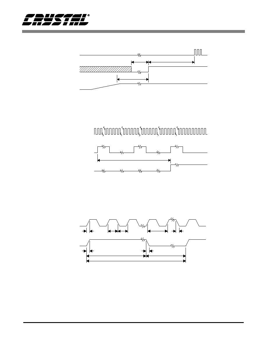
CS4205
DS489PP2
11
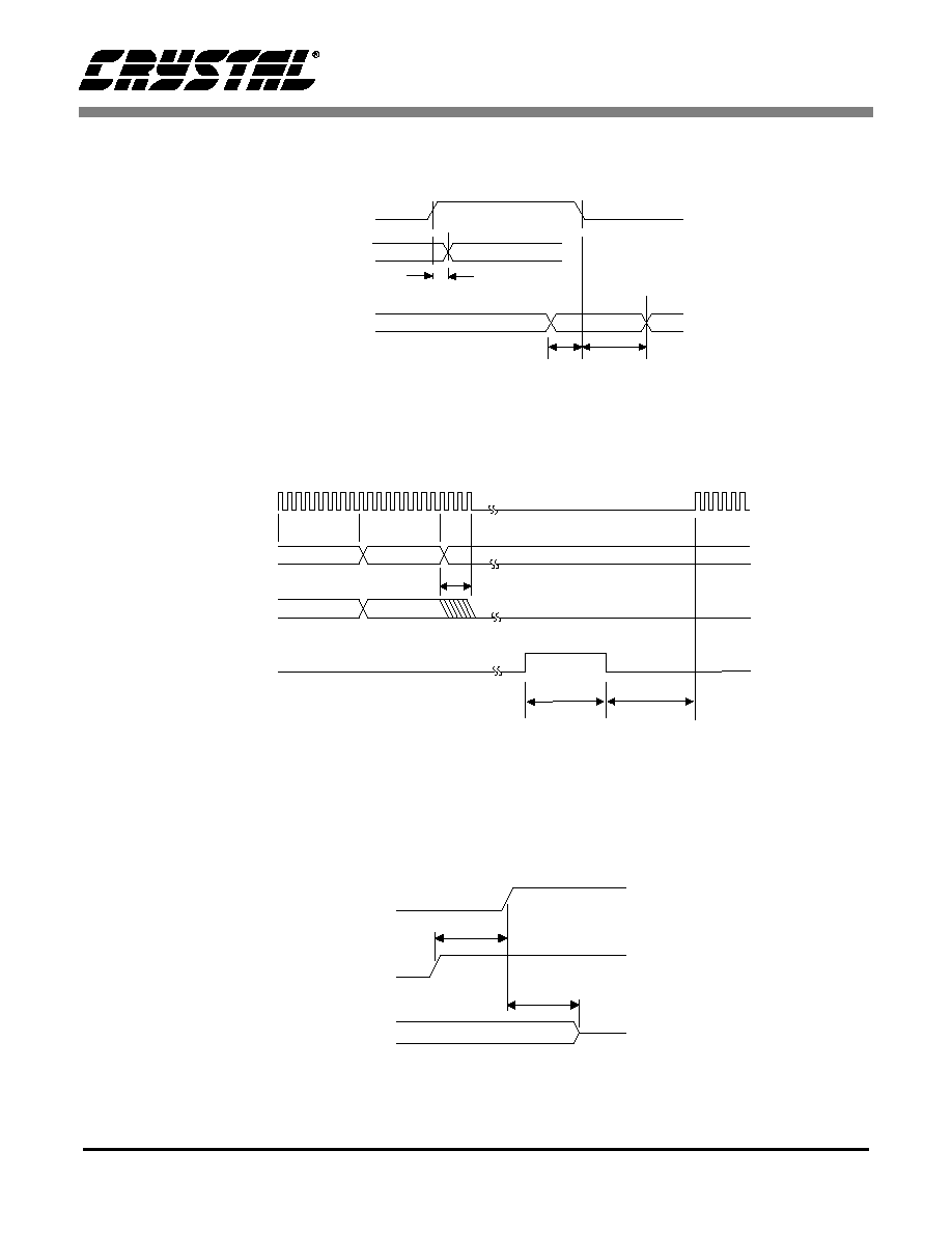
BIT_CLK
T
rst_low
T
rst2clk
T
vdd2rst#
Vdd
RESET#
Figure 1. Power Up Timing
Figure 2. Codec Ready from Start-up or Fault Condition
BIT_CLK
T
sync2crd
CODEC_READY
SYNC
Figure 3. Clocks
BIT_CLK
SYNC
T
irise
T
ifall
T
orise
T
ifall
T
clk_high
T
clk_low
T
sync_high
T
sync_low
T
sync_period
T
clk_period
CS4205
12
DS489PP2
BIT_CLK
T
isetup
T
ihold
T
co
SDATA_OUT,
SYNC
SDATA_IN
Figure 4. Data Setup and Hold
BIT_CLK
T
s2_pdown
SDATA_IN
SDATA_OUT
SYNC
Write to 0x20
Data PR4
Don't Care
Slot 1
Slot 2
sync_pr4
sync2clk
T
T
Figure 5. PR4 Powerdown and Warm Reset
RESET#
SDATA_OUT,
SYNC
T
setup2rst
SDATA_IN,
T
off
BIT_CLK
Hi-Z
Figure 6. Test Mode
CS4205
DS489PP2
13
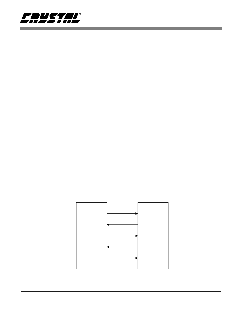
2. GENERAL DESCRIPTION
The CS4205 is a mixed-signal serial audio codec
compliant with the Intel
Æ
Audio Codec '97 Specifi-
cation, revision 2.1 [6] (referred to as AC '97). It is
designed to be paired with a digital controller, typ-
ically located on the PCI bus or integrated within
the system core logic chip set. The controller is re-
sponsible for all communications between the
CS4205 and the remainder of the system. The
CS4205 contains two distinct functional sections:
digital and analog. The digital section includes the
AC-link interface, S/PDIF interface, serial data
port, GPIO, signal processing engine, ZV Port,
power management support, and Sample Rate Con-
verters (SRCs). The analog section includes the an-
alog input multiplexer (mux), stereo input mixer,
stereo output mixer, mono output mixer, stereo An-
alog-to-Digital Converters (ADCs), stereo Digi-
tal-to-Analog Converters (DACs), dedicated mono
microphone ADC, and their associated volume
controls.
2.1
AC-Link
All communication with the CS4205 is established
with a 5-wire digital interface to the controller
called the AC-link. This interface is shown in
Figure 7. All clocking for the serial communication
is synchronous to the BIT_CLK signal. BIT_CLK
is generated by the primary audio codec and is used
to clock the controller and any secondary audio co-
decs. Both input and output AC-link audio frames
are organized as a sequence of 256 serial bits form-
ing 13 groups referred to as `slots'. During each au-
dio frame, data is passed bi-directionally between
the CS4205 and the controller. The input frame is
driven from the CS4205 on the SDATA_IN line.
The output frame is driven from the controller on
the SDATA_OUT line. The controller is also re-
sponsible for issuing reset commands via the RE-
SET# signal. Following a Cold Reset, the CS4205
is responsible for notifying the controller that it is
ready for operation after synchronizing its internal
functions. The CS4205 AC-link signals must use
the same digital supply voltage as the controller, ei-
ther +5 V or +3.3 V. See Section 4, AC-Link Frame
Definition, for detailed AC-link information.
CODEC
SYNC
BIT_CLK
SDATA_OUT
SDATA_IN
RESET#
Digital AC'97
Controller
AC'97
Figure 7. AC-link Connections

CS4205
14
DS489PP2
2.2
Control Registers
The CS4205 contains a set of AC '97 compliant
control registers, and a set of Cirrus Logic defined
control registers. These registers control the basic
functions and features of the CS4205. Read access-
es of the control registers by the AC '97 controller
are accomplished with the requested register index
in Slot 1 of a SDATA_OUT frame. The following
SDATA_IN frame will contain the read data in its
Slot 2. Write operations are similar, with the regis-
ter index in Slot 1 and the write data in Slot 2 of a
SDATA_OUT frame. The function of each input
and output frame is detailed in Section 4, AC-Link
Frame Definition. Individual register descriptions
are found in Section 5, Register Interface.
2.3
Sample Rate Converters
The sample rate converters (SRC) provide high ac-
curacy digital filters supporting sample frequencies
other than 48 kHz to be captured from the CS4205
or played from the controller. AC '97 requires sup-
port for two audio rates (44.1 and 48 kHz) and four
modem rates (8, 9.6, 13.714, and 16 kHz). In addi-
tion, the Intel
Æ
I/O Controller Hub (ICHx) specifi-
cation [9] requires support for five more audio rates
(8, 11.025, 16, 22.05, and 32 kHz) and specifies
two optional modem rates (24, 48kHz). The
CS4205 supports all these rates, as shown in
Table 12 on page 37.
2.4
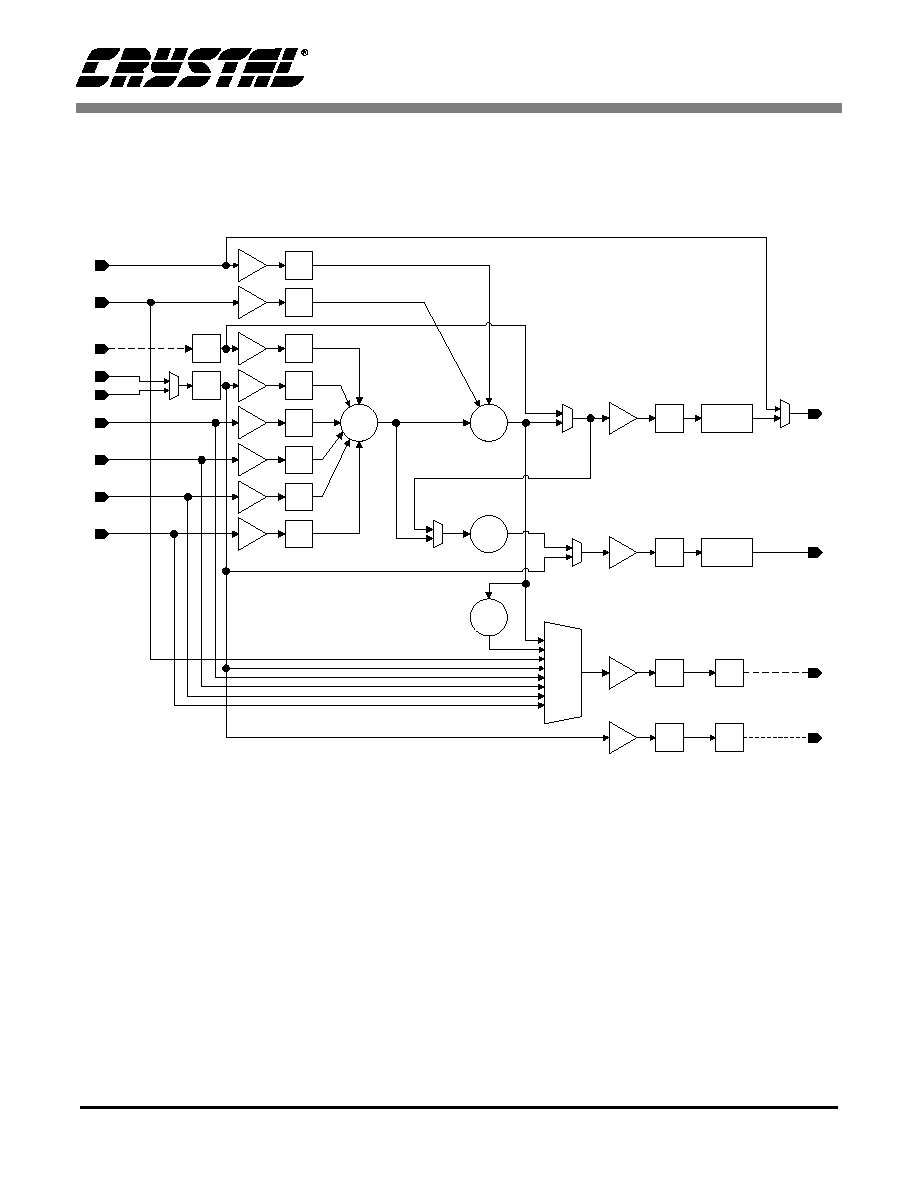
Mixers
The CS4205 input and output mixers are illustrated
in Figure 8. The stereo input mixer sums together
the analog inputs to the CS4205 according to the
settings in the volume control registers. The stereo
output mixer sums the output of the stereo input
mixer with the PC_BEEP and PHONE signals. The
stereo output mix is then sent to the LINE_OUT
pins of the CS4205. The mono output mixer gener-
ates a monophonic sum of the left and right audio
channels from the stereo input mixer. The mono
output mix is then sent to the MONO_OUT pin on
the CS4205.
2.5
Input Mux
The input multiplexer controls which analog input
is sent to the ADCs. The output of the input mux is
converted to stereo 18-bit digital PCM data and
transmitted to the controller by means of the
AC-link SDATA_IN signal.
2.6
Volume Control
The CS4205 volume registers control analog input
levels to the input mixer and analog output levels,
including the master volume level. The PC_BEEP
volume control uses 3 dB steps with a range of 0 dB
to -45 dB attenuation. All other analog volume con-
trols use 1.5 dB steps. The analog inputs have a
mixing range of +12 dB signal gain to -34.5 dB sig-
nal attenuation. The analog output volume controls
have from 0 dB to -46.5 dB attenuation for
LINE_OUT and MONO_OUT.
2.7
Dedicated Mic Record Path
The CS4205 includes a dedicated microphone
ADC that supports advanced functions such as
speech recognition and internet telephony. The
dedicated ADC allows recording of a microphone
input independent of the input mux settings. This
enables simultaneous capture of microphone and
independent stereo sources.
CS4205
DS489PP2
15
VO
L
MUTE
VO
L
MUTE
VO
L
MUTE
VO
L
VO
L
MUTE
VO
L
VO
L
VO
L
MUTE
BOOST
1/2
OUTPUT
BUFFER
OUTPUT
BUFFER
VO
L
ADC
INPUT
MUX
VO
L
ADC
MUTE
PCM_OUT
PC_BEEP
PHONE
MIC1
MIC2
LINE
CD
VIDEO
AUX
ANALOG STEREO
OUTPUT MIXER
MASTER
VOLUME
MONO
VOLUME
MONO OUT
SELECT
STEREO TO
MONO MIXER
L/R ADC
GAIN
L/R A/D
CONVERTERS
MIC
SELECT
MONO OUT
LINE OUT
PCM_IN
DAC
Front D/A
CONVERTERS
1/2
STEREO TO
MONO MIXER
MUTE
MUTE
VO
L
MUTE
MUTE
MUTE
DAC DIRECT
MODE
PC BEEP BYPASS
MONO MIX
SELECT
VO
L
ADC
MUTE
MIC ADC
GAIN
MIC A/D
CONVERTER
MIC_PCM_IN
ANALOG STEREO
INPUT MIXER
Figure 8. CS4205 Mixer Diagram
CS4205
16
DS489PP2
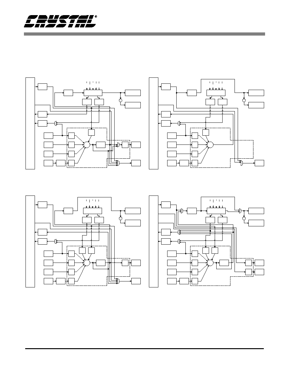
3. DIGITAL SIGNAL PATHS
The CS4205 includes a number of internal digital
signal path options. Figure 9 shows the principal
signal flow options through one channel of the de-
vice. Four commonly used signal flow modes are
detailed in the following sections. The signal flow
modes are controlled through the bits in the AC
Mode Control Register (Index 5Eh). The bit config-
uration for each detailed mode is listed in Table 1
on page 17.
3.1
Analog Centric Mode
Analog centric mode is detailed in Figure 10 on
page 18. In this mode, all the digital sources are
pre-mixed in the digital mixer and sent to the
DACs. The DAC outputs are mixed with the analog
sources in the analog mixer. The ADCs send cap-
tured data directly to the host. The ADC mux is
used to select a single source or the output of the in-
put mixer for capture. In the analog centric mode,
effects processing is only available on digital
sources.
Signal Processing Engine
SRC
DAC
LINE_OUT
MONO_OUT
ADC
Ω ADC
SRC
Ω SRC
I≤S
IN1
I≤S
IN2
I≤S
IN3
ZV
ASRC
VOL
VOL
VOL
VOL
DIG
EFX
I≤S
OUT1
S/PDIF
OUT
I≤S
OUT2
VOL
VOL
VOL
VOL
DACS
CAPS
MICS
DDM
SDOS
SPDS
AC-Link
front
ch
L/R
cap
mic
cap
surr
ch
c+lfe
ch
MIXER
LI
NE
CD
VI
DEO
AUX
MIC
mux out
m
i
x
out
mic out
Figure 9. Digital Signal Path Overview
CS4205
DS489PP2
17
3.2
Digital Centric Mode
Digital centric mode is detailed in Figure 11. In this
mode, the analog sources are first mixed in the an-
alog mixer and sent to the ADCs. The ADC outputs
are then mixed with the digital sources in the digital
mixer. This allows effects processing on all sources
and supports a "what you hear is what you record"
model. The processed digital signal is sent to the
DACs, bypassing the analog mixer using DAC di-
rect mode. The ADC mux must be set to stereo mix
to support this model. Consequently, only the mix
can be captured by the host, rather than the individ-
ual sources.
3.3
Host Processing Mode
Host processing mode is detailed in Figure 12. This
mode is similar to digital centric mode, except the
output of the digital mixer is captured by the host.
Any mixing with host sources and effects process-
ing is done on the host. The processed signal is sent
to the DACs, bypassing the analog mixer using
DAC direct mode. In host processing mode, the
playback and capture paths are completely separate
inside the CS4205.
3.4
Multi-Channel Mode
Multi-channel mode is detailed in Figure 13. This
mode is an extension of any of the other three
modes, with the distinguishing feature that one or
two additional slot pairs are routed to the serial data
output ports. This allows for a complete
multi-channel solution with a single AC '97 audio
codec and external DACs.
AC Mode
Control Bits
Analog Centric
Mode
Digital Centric
Mode
Host Processing
Mode
Multi-Channel
Mode
DACS
1
1
0
0 or 1
CAPS[1:0]
00
10
10
00,10 or 11
MICS
0 or 1
0 or 1
0 or 1
0 or 1
DDM
0
1
1
0 or 1
SDOS[1:0]
10 or 11
11
-
00
SPDS[1:0]
00, 01, 10 or 11
00, 01, 10 or 11
00 or 01
N/A
Table 1. AC Mode Control Configurations
CS4205
18
DS489PP2
Signal Processing Engine
AC-Link
SRC
DAC
MIXER
LINE_OUT
LI
NE
CD
VI
D
E
O
AU
X
MI
C
MONO_OUT
ADC
Ω ADC
SRC
Ω SRC
I≤S
IN1
I≤S
IN2
I≤S
IN3
ZV
ASRC
VOL
VOL
VOL
VOL
DIG
EFX
I≤S
OUT1
S/PDIF
OUT
mux out
m
i
x
out
mic out
VOL
VOL
front
ch
L/R
cap
mic
cap
surr
ch
c+lfe
ch
MICS
SDOS
SPDS
Figure 10. Analog Centric Mode
Signal Processing Engine
SRC
DAC
LINE_OUT
MONO_OUT
ADC
Ω ADC
SRC
Ω SRC
I≤S
IN1
I≤S
IN2
I≤S
IN3
ZV
ASRC
VOL
VOL
VOL
VOL
DIG
EFX
I≤S
OUT1
S/PDIF
OUT
VOL
VOL
VOL
MICS
SPDS
AC-Link
front
ch
L/R
cap
mic
cap
surr
ch
c+lfe
ch
MIXER
LI
NE
CD
VI
D
E
O
AU
X
MI
C
mux out
m
i
x
out
mic out
Figure 11. Digital Centric Mode
Signal Processing Engine
SRC
DAC
LINE_OUT
MONO_OUT
ADC
Ω ADC
SRC
Ω SRC
I≤S
IN1
I≤S
IN2
I≤S
IN3
ZV
ASRC
VOL
VOL
VOL
VOL
S/PDIF
OUT
VOL
MICS
SPDS
AC-Link
front
ch
L/R
cap
mic
cap
surr
ch
c+lfe
ch
MIXER
LI
NE
CD
VI
D
E
O
AU
X
MI
C
mux out
m
i
x
out
mic out
Figure 12. Host Processing Mode
Signal Processing Engine
SRC
DAC
LINE_OUT
MONO_OUT
ADC
Ω ADC
SRC
Ω SRC
I≤S
IN1
I≤S
IN2
I≤S
IN3
ZV
ASRC
VOL
VOL
VOL
VOL
DIG
EFX
I≤S
OUT1
I≤S
OUT2
VOL
VOL
VOL
VOL
DACS
CAPS
MICS
DDM
AC-Link
front
ch
L/R
cap
mic
cap
surr
ch
c+lfe
ch
MIXER
LI
NE
CD
VI
D
E
O
AU
X
MI
C
mux out
m
i
x
out
mic out
Figure 13. Multi-Channel Mode
CS4205
DS489PP2
19
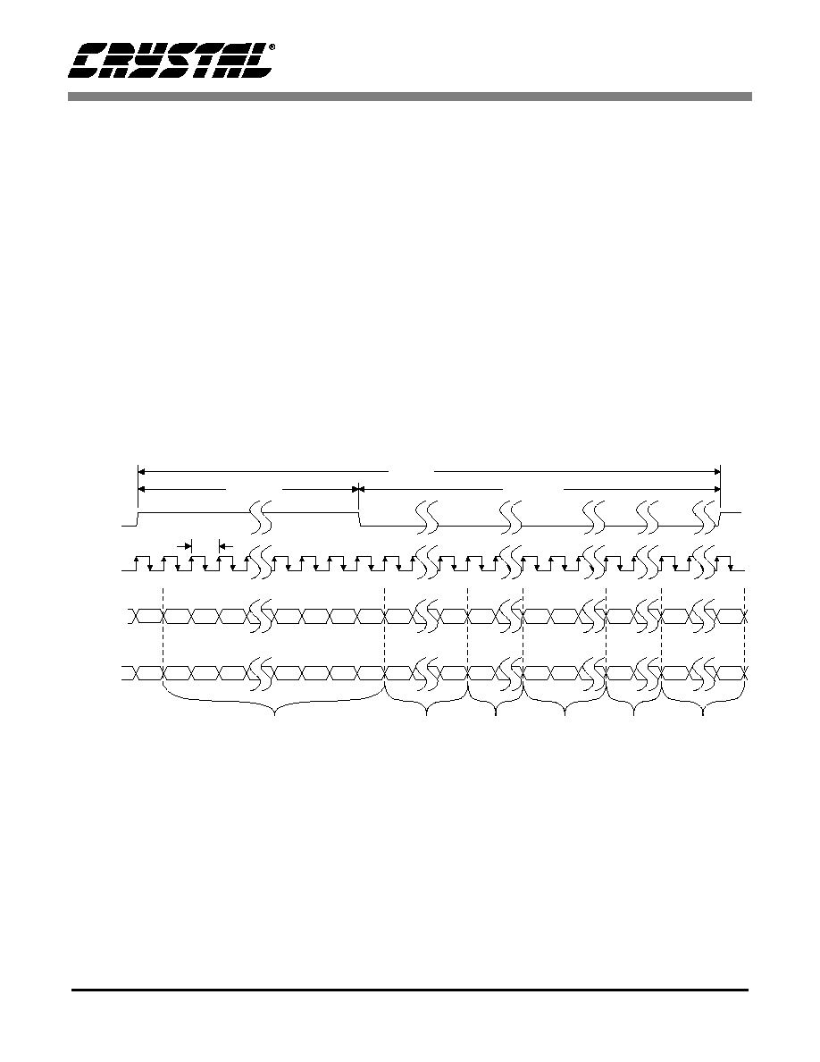
4. AC-LINK FRAME DEFINITION
The AC-link is a bi-directional serial port with data
organized into frames consisting of one 16-bit and
twelve 20-bit time-division multiplexed slots.
Slot 0 is a special reserved time slot containing
16-bits which are used for AC-link protocol infra-
structure. Slots 1 through 12 contain audio or con-
trol/status data. Both the serial data output and
input frames are defined from the controller per-
spective, not from the CS4205 perspective.
The controller synchronizes the beginning of a
frame with the assertion of the SYNC signal.
Figure 14 shows the position of each bit location
within the frame. The first bit position in a new se-
rial data frame is F0 and the last bit position in the
serial data frame is F255. When SYNC goes active
(high) and is sampled active by the CS4205 (on the
falling edge of BIT_CLK), both devices are syn-
chronized to a new serial data frame. The data on
the SDATA_OUT pin at this clock edge is the final
bit of the previous frame's serial data. On the next
rising edge of BIT_CLK, the first bit of Slot 0 is
driven by the controller on the SDATA_OUT pin.
On the next falling edge of BIT_CLK, the CS4205
latches this data in as the first bit of the frame.
20.8
µs
(48 kHz)
Tag Phase
Data Phase
12.288 MHz
81.4 ns
SYNC
BIT_CLK
SDATA_OUT
SDATA_IN
F0
F1
F2
F16
F15
F14
F13
F12
F35
F56
F76
D19
F255
Valid
Frame
Slot 1
Valid
0
R/W
0
WD15
F36
F57
D19
D18
D19
D19
D18
D19
RD15
0
0
0
0
F0
F1
F2
F16
F15
F14
F13
F12
F35
F56
F76
F255
F36
F57
F255
F255
0
0
GPIO
INT
F96
F96
D19
Slot 0
Slot 1
Slot 2
Slot 3
Slot 4
Slots 5-12
Slot 2
Valid
Slot 1
Valid
Slot 2
Valid
Codec
Ready
0
Slot 12
Valid
Codec
ID1
Codec
ID0
Slot 12
Valid
GPIO
INT
Bit Frame Position:
Bit Frame Position:
Figure 14. AC-link Input and Output Framing

CS4205
20
DS489PP2
4.1
AC-Link Serial Data Output Frame
In the serial data output frame, data is passed on the SDATA_OUT pin to the CS4205 from the AC '97
controller. Figure 14 illustrates the serial port timing.
The PCM playback data being passed to the CS4205 is shifted out MSB first in the most significant bits
of each slot. Any PCM data from the AC '97 controller that is not 20 bits wide should be left justified in
its corresponding slot and dithered or zero-padded in the unused bit positions.
Bits that are reserved should always be `cleared' by the AC '97 controller.
4.1.1
Serial Data Output Slot Tags (Slot 0)
Valid Frame
The Valid Frame bit determines if any of the following slots contain either valid playback data
for the CS4205 or data for read/write operations. When `set', at least one of the other AC-link
slots contains valid data. If this bit is `clear', the remainder of the frame is ignored.
Slot 1 Valid
The Slot 1 Valid bit indicates a valid register read/write address for a primary codec.
Slot 2 Valid
The Slot 2 Valid bit indicates valid register write data for a primary codec.
Slot [3:11] Valid
The Slot [3:11] Valid bits indicate the validity of data in their corresponding serial data output
slots. If a bit is `set', the corresponding output slot contains valid data. If a bit is `cleared', the
corresponding slot will be ignored.
Slot 12 Valid
The Slot 12 Valid bit indicates if output Slot 12 contains valid GPIO control data.
Codec ID[1:0]
The Codec ID[1:0] bits determine which codec is being accessed during the current AC-link
frame. Codec ID[1:0] = 00 indicates the primary codec is being accessed. Codec ID[1:0] = 01,
10, or 11 indicates one of three possible secondary codecs is being accessed. A Codec ID
value of 01, 10, or 11 also indicates a valid read/write address and/or valid register write data
for a secondary codec.
4.1.2
Command Address Port (Slot 1)
R/W Read/Write. When this bit is `set', a read of the AC '97 register specified by the register index
bits will occur in the AC '97 2.x audio codec. When the bit is `cleared', a write will occur. For
any read or write access to occur, the Valid Frame bit (F0) must be `set' and the Codec ID[1:0]
bits (F[14:15]) must match the Codec ID of the AC '97 2.x audio codec being accessed. Ad-
ditionally, for a primary codec, the Slot 1 Valid bit (F1) must be `set' for a read access and
both the Slot 1 Valid bit (F1) and the Slot 2 Valid bit (F2) must be `set' for a write access. For
a secondary codec, both the Slot 1 Valid bit (F1) and the Slot 2 Valid bit (F2) must be `cleared'
for read and write accesses. See Figure 14 for bit frame positions.
RI[6:0]
Register Index. The RI[6:0] bits contain the 7-bit register index to the AC '97 registers in the
CS4205. All registers are defined at word addressable boundaries. The RI0 bit must be `clear'
to access CS4205 registers.
Bit 15
14
13
12
11
10
9
8
7
6
5
4
3
2
1
0
Valid
Frame
Slot 1
Valid
Slot 2
Valid
Slot 3
Valid
Slot 4
Valid
Slot 5
Valid
Slot 6
Valid
Slot 7
Valid
Slot 8
Valid
Slot 9
Valid
Slot 10
Valid
Slot 11
Valid
Slot 12
Valid
Res
Codec
ID1
Codec
ID0
Bit 19
18
17
16
15
14
13
12
11
10
9
8
7
6
5
4
3
2
1
0
R/W
RI6
RI5
RI4
RI3
RI2
RI1
RI0
Reserved

CS4205
DS489PP2
21
4.1.3
Command Data Port (Slot 2)
WD[15:0]
Write Data. The WD[15:0] bits contain the 16-bit value to be written to the register. If an ac-
cess is a read, this slot is ignored.
NOTE:
For any write to an AC '97 register, the write is defined to be an `atomic' access. This means
that when the Slot 1 Valid bit in output Slot 0 is `set', the Slot 2 Valid bit in output Slot 0 should
always be `set' during the same audio frame. No write access may be split across 2 frames.
4.1.4
PCM Playback Data (Slots 3-11)
PD[19:0]
Playback Data. The PD[19:0] bits contain the 20-bit PCM (2's complement) playback data for
the left and right DACs, serial data ports, and/or the S/PDIF transmitter. Table 14 on page 42
lists a cross reference for each function and its respective slot. The mapping of a given slot
to the DAC, serial data port, or S/PDIF transmitter is determined by the state of the ID[1:0]
bits in the Extended Audio ID Register (Index 28h) and by the SM[1:0] and AMAP bits in the
AC Mode Control Register (Index 5Eh).
4.1.5
GPIO Pin Control (Slot12)
GPIO[4:0]
GPIO Pin Control. The GPIO[4:0] bits control the CS4205 GPIO pins configured as outputs.
Write accesses using GPIO pin control bits configured at outputs will be reflected on the GPIO
pin output on the next AC-link frame. Write accesses using GPIO pin control bits configured
as inputs will have no effect and are ignored. If the GPOC bit in the Misc. Crystal Control Reg-
ister (Index 60h) is `set', the bits in output Slot 12 are ignored and GPIO pins configured as
outputs are controlled through the GPIO Pin Status Register (Index 54h).
Bit 19
18
17
16
15
14
13
12
11
10
9
8
7
6
5
4
3
2
1
0
WD15 WD14 WD13 WD12 WD11 WD10 WD9 WD8 WD7 WD6 WD5 WD4 WD3 WD2 WD1 WD0
Reserved
Bit 19
18
17
16
15
14
13
12
11
10
9
8
7
6
5
4
3
2
1
0
PD19 PD18 PD17 PD16 PD15 PD14 PD13 PD12 PD11 PD10 PD9 PD8 PD7 PD6 PD5 PD4 PD3 PD2 PD1 PD0
Bit 19 18
17
16
15
14
13
12
11
10
9
8
7
6
5
4
3
2
1
0
Not Implemented
GPIO4 GPIO3 GPIO2 GPIO1 GPIO0
Reserved
CS4205
22
DS489PP2
4.2
AC-Link Serial Data Input Frame
In the serial data input frame, data is passed on the SDATA_IN pin from the CS4205 to the AC '97 con-
troller. The data format for the input frame is very similar to the output frame. Figure 14 on page 19 illus-
trates the serial port timing.
The PCM capture data from the CS4205 is shifted out MSB first in the most significant 18 bits of each slot.
The least significant 2 bits in each slot will be `cleared'. If the host requests PCM data from the AC '97
Controller that is less than 18 bits wide, the controller should dither and round or just round (but not trun-
cate) to the desired bit depth.
Bits that are reserved or not implemented in the CS4205 will always be returned `cleared'.
4.2.1
Serial Data Input Slot Tag Bits (Slot 0)
Codec Ready
Codec Ready. The Codec Ready bit indicates the readiness of the CS4205 AC-link. Immedi-
ately after a Cold Reset this bit will be `clear'. Once the CS4205 clocks and voltages are sta-
ble, this bit will be `set'. Until the Codec Ready bit is `set', no AC-link transactions should be
attempted by the controller. The Codec Ready bit does not indicate readiness of the DACs,
ADCs, Vref, or any other analog function. Those must be checked in the Powerdown Con-
trol/Status Register (Index 26h) by the controller before any access is made to the mixer reg-
isters. Any accesses to the CS4205 while Codec Ready is `clear' are ignored.
Slot 1 Valid
The Slot 1 Valid bit indicates Slot 1 contains a valid read back address.
Slot 2 Valid
The Slot 2 Valid bit indicates Slot 2 contains valid register read data.
Slot [3:8,11] Valid
The Slot [3:8,11] Valid bits indicate Slot [3:8,11] contains valid capture data from the CS4205
ADCs. If a bit is `set', the corresponding input slot contains valid data. If a bit is `cleared', the
corresponding slot will be ignored.
Slot 12 Valid
The Slot 12 Valid bit indicates Slot 12 contains valid GPIO status data.
4.2.2
Status Address Port (Slot 1)
RI[6:0]
Register Index. The RI[6:0] bits echo the AC '97 register address when a register read has
been requested in the previous frame. The CS4205 will only echo the register index for a read
access. Write accesses will not return valid data in Slot 1.
SR[3:9,11]
Slot Request. If SRx is `set', this indicates the CS4205 SRC does not need a new sample on
the next AC-link frame for that particular slot. If SRx is `clear', the SRC indicates a new sample
is needed on the following frame. If the VRA bit in the Extended Audio Status/Control Register
(Index 2Ah)
is `clear', the SR[3:9,11] bits are always 0. When VRA is `set', the SRC is enabled
and the SR[3:9,11] bits are used to request data.
Bit 15
14
13
12
11
10
9
8
7
6
5
4
3
2
1
0
Codec
Ready
Slot 1
Valid
Slot 2
Valid
Slot 3
Valid
Slot 4
Valid
Slot 5
Valid
Slot 6
Valid
Slot 7
Valid
Slot 8
Valid
0
0
Slot 11
Valid
Slot 12
Valid
Reserved
Bit 19
18
17
16
15
14
13
12
11
10
9
8
7
6
5
4
3
2
1
0
Res
RI6
RI5
RI4
RI3
RI2
RI1
RI0
SR3 SR4 SR5 SR6 SR7 SR8 SR9
0
SR11
0
Reserved

CS4205
DS489PP2
23
4.2.3
Status Data Port (Slot 2)
RD[15:0]
Read Data. The RD[15:0] bits contain the register data requested by the controller from the
previous read request. All read requests will return the read address in the input Slot 1 and
the register data in the input Slot 2 on the following serial data frame.
4.2.4
PCM Capture Data (Slot 3-8)
CD[17:0]
Capture Data. The CD [17:0] bits contain 18-bit PCM (2's complement) capture data. The
data will only be valid when the respective slot valid bit is `set' in input Slot 0. The mapping of
a given slot to an ADC is determined by the state of the ID[1:0] bits in the Extended Audio ID
Register (Index 28h) and the SM[1:0] and AMAP bits in the AC Mode Control Register (Index
5Eh). The definition of each slot can be found in Table 14 on page 42.
4.2.5
GPIO Pin Status (Slot 12)
GPIO[4:0]
GPIO Pin Status. The GPIO[4:0] bits reflect the status of the CS4205 GPIO pins configured
as inputs. The pin status of GPIO pins configured as outputs will be reflected back on the
GPIO[4:0] bits of input Slot 12 in the next frame. The output GPIO pins are controlled by the
GPIO[4:0] pin control bits in output Slot 12.
BDI
BIOS-Driver Interface. The BDI bit indicates that a BIOS event has occurred. This bit is a logic
OR of all bits in the BDI Status Register (Index 7Ah) ANDed with their corresponding bit in the
BDI Config Register (Index 6Eh, Address 0Ch).
IEC
Internal Error Condition. The IEC bit indicates that an internal error, such as an ADC over-
range or a digital data overflow has occurred. This bit is a logic OR of all bits in the IEC Status
Register (Index 6Eh, Address 0Bh).
GPIO_INT
GPIO Interrupt. The GPIO_INT bit indicates that a GPIO, BDI, or IEC interrupt event has oc-
curred. The occurrence of a GPIO interrupt is determined by the GPIO interrupt requirements
as outlined in the GPIO Pin Wakeup Mask Register (Index 52h) description. In this case, the
GPIO_INT bit is cleared by writing a `0' to the bit in the GPIO Pin Status Register (Index 54h)
corresponding to the GPIO pin which generated the interrupt.
The occurrence of a BDI interrupt is determined by the BDI interrupt requirements as outlined
in the BIOS-Driver Interface Control Registers (Index 6Eh, Address 0C-0Dh). In this case, the
GPIO_INT bit is cleared by writing a `0' to the bit in the BDI Status Register (Index 7Ah) that
generated the interrupt.
The occurrence of an IEC interrupt is determined by the IEC interrupt requirements as out-
lined in the Internal Error Condition Control/Status Registers (Index 6Eh, Address 09h - 0Bh).
In this case, the GPIO_INT bit is cleared by writing a `0' to the bit in the IEC Status Register
(Index 6Eh, Address 0Bh) corresponding to the IEC source which generated the interrupt.
Bit 19
18
17
16
15
14
13
12
11
10
9
8
7
6
5
4
3
2
1
0
RD15 RD14 RD13 RD12 RD11 RD10 RD9 RD8 RD7 RD6 RD5 RD4 RD3 RD2 RD1 RD0
Reserved
Bit 19
18
17
16
15
14
13
12
11
10
9
8
7
6
5
4
3
2
1
0
CD17 CD16 CD15 CD14 CD13 CD12 CD11 CD10 CD9 CD8 CD7 CD6 CD5 CD4 CD3 CD2 CD1 CD0
0
0
Bit 19 18
17
16
15
14
13
12
11
10
9
8
7
6
5
4
3
2
1
0
0
0
0
0
0
0
0
0
0
0
0
GPIO4 GPIO3 GPIO2 GPIO1 GPIO0 Res BDI IEC
GPIO
_INT

CS4205
24
DS489PP2
4.3
AC-Link Protocol Violation - Loss of
SYNC
The CS4205 is designed to handle SYNC protocol
violations. The following are situations where the
SYNC protocol has been violated:
∑
The SYNC signal is not sampled high for exact-
ly 16 BIT_CLK clock cycles at the start of an
audio frame.
∑
The SYNC signal is not sampled high on the
256th BIT_CLK clock period after the previous
SYNC assertion.
∑
The SYNC signal goes active high before the
256th BIT_CLK clock period after the previous
SYNC assertion.
Upon loss of synchronization with the controller,
the CS4205 will `clear' the Codec Ready bit in the
serial data input frame until two valid frames are
detected. During this detection period, the CS4205
will ignore all register reads and writes and will
discontinue the transmission of PCM capture data.
In addition, if the LOSM bit in the Misc. Crystal
Control Register (Index 60h) is `set' (default), the
CS4205 will mute all analog outputs. If the LOSM
bit is `clear', the analog outputs will not be muted.
CS4205
DS489PP2
25
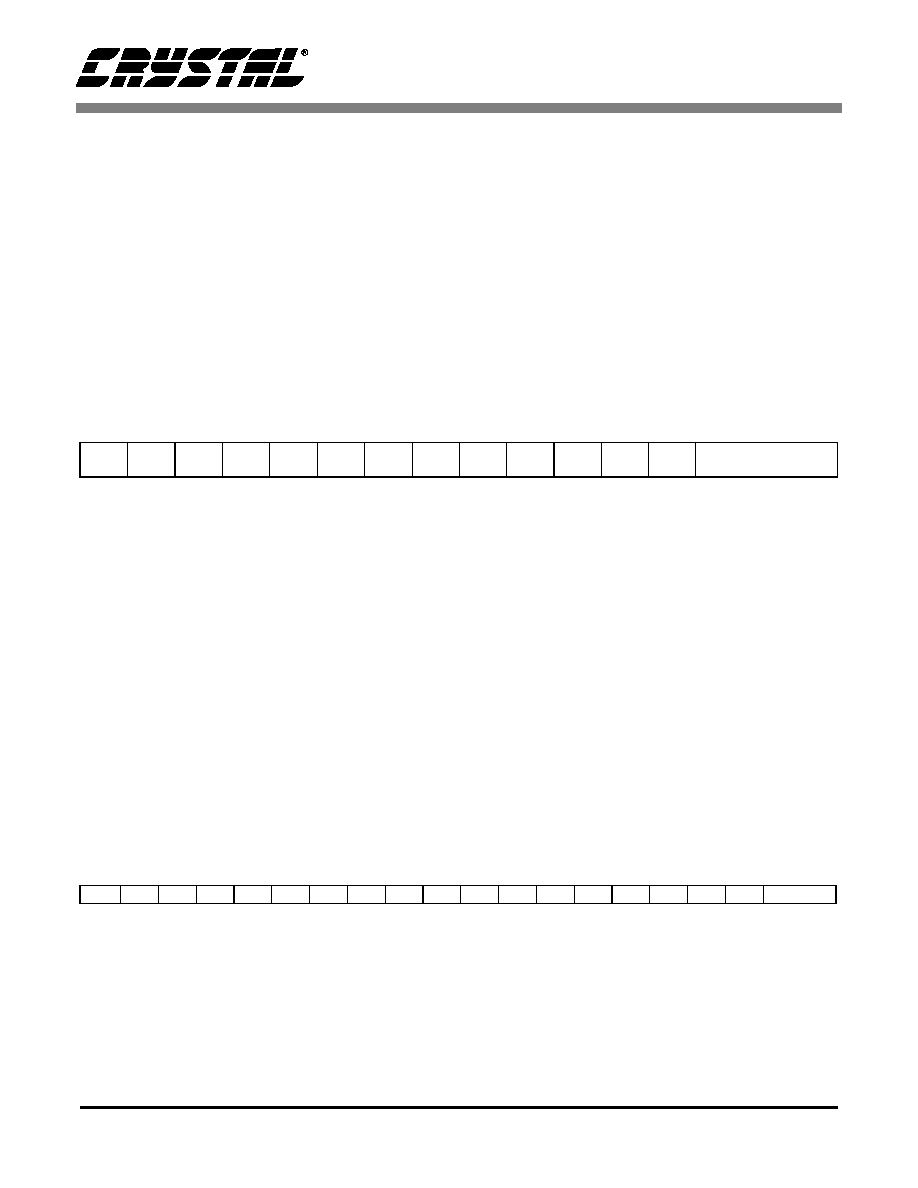
5. REGISTER INTERFACE
Reg
Register Name
D15 D14
D13
D12 D11 D10
D9
D8
D7
D6
D5
D4
D3
D2
D1
D0
Default
00h
Reset
0
SE4
SE3
SE2
SE1
SE0
0
ID8
ID7
0
ID5
0
ID3
ID2
0
ID0
25ADh
02h
Master Volume
Mute
0
ML5
ML4
ML3
ML2
ML1
ML0
0
0
MR5
MR4
MR3
MR2
MR1
MR0
8000h
06h
Mono Volume
Mute
0
0
0
0
0
0
0
0
0
MM5
MM4
MM3
MM2
MM1
MM0
8000h
08h
Master Tone Control
0
0
0
0
BA3
BA2
BA1
BA0
0
0
0
0
TR3
TR2
TR1
TR0
0F0Fh
0Ah
PC_BEEP Volume
Mute
0
0
0
0
0
0
0
0
0
0
PV3
PV2
PV1
PV0
0
0000h
0Ch
Phone Volume
Mute
0
0
0
0
0
0
0
0
0
0
GN4
GN3
GN2
GN1
GN0
8008h
0Eh
Mic Volume
Mute
0
0
0
0
0
0
0
0
20dB
0
GN4
GN3
GN2
GN1
GN0
8008h
10h
Line In Volume
Mute
0
0
GL4
GL3
GL2
GL1
GL0
0
0
0
GR4
GR3
GR2
GR1
GR0
8808h
12h
CD Volume
Mute
0
0
GL4
GL3
GL2
GL1
GL0
0
0
0
GR4
GR3
GR2
GR1
GR0
8808h
14h
Video Volume
Mute
0
0
GL4
GL3
GL2
GL1
GL0
0
0
0
GR4
GR3
GR2
GR1
GR0
8808h
16h
Aux Volume
Mute
0
0
GL4
GL3
GL2
GL1
GL0
0
0
0
GR4
GR3
GR2
GR1
GR0
8808h
18h
PCM Out Volume
Mute
0
0
GL4
GL3
GL2
GL1
GL0
0
0
0
GR4
GR3
GR2
GR1
GR0
8808h
1Ah
Record Select
0
0
0
0
0
SL2
SL1
SL0
0
0
0
0
0
SR2
SR1
SR0
0000h
1Ch
Record Gain
Mute
0
0
0
GL3
GL2
GL1
GL0
0
0
0
0
GR3
GR2
GR1
GR0
8000h
1Eh
Record Gain Mic
Mute
0
0
0
0
0
0
0
0
0
0
0
GM3
GM2
GM1
GM0
8000h
20h
General Purpose
POP
ST
3D
LD
0
0
MIX
MS
LPBK
0
0
0
0
0
0
0
0000h
22
3D Control
0
0
0
0
CR3
CR2
CR1
CR0
0
0
0
0
DP3
DP2
DP1
DP0
0000h
26h
Powerdown Ctrl/Stat
EAPD
0
PR5
PR4
PR3
PR2
PR1
PR0
0
0
0
0
REF
ANL
DAC
ADC
000Fh
28h
Ext'd Audio ID
ID1
ID0
0
0
0
0
AMAP
0
0
0
0
0
VRM
0
0
VRA
x209h
2Ah
Ext'd Audio Stat/Ctrl
0
PRL
0
0
0
0
MADC
0
0
0
0
0
VRM
0
0
VRA
4000h
2Ch
PCM Front DAC Rate
SR15
SR14
SR13
SR12
SR11 SR10
SR9
SR8
SR7
SR6
SR5
SR4
SR3
SR2
SR1
SR0
BB80h
32h
PCM L/R ADC Rate
SR15
SR14
SR13
SR12
SR11 SR10
SR9
SR8
SR7
SR6
SR5
SR4
SR3
SR2
SR1
SR0
BB80h
34h
Mic ADC Rate
SR15
SR14
SR13
SR12
SR11 SR10
SR9
SR8
SR7
SR6
SR5
SR4
SR3
SR2
SR1
SR0
BB80h
3Ch
Ext'd Modem ID
ID1
ID0
0
0
0
0
0
0
0
0
0
0
0
0
0
0
x000h
3Eh
Ext'd Modem Stat/Ctrl
0
0
0
0
0
0
0
PRA
0
0
0
0
0
0
0
GPIO
0100h
4Ch
GPIO Pin Config.
0
0
0
0
0
0
0
0
0
0
0
GC4
GC3
GC2
GC1
GC0
001Fh
4Eh
GPIO Pin Polarity/Type
1
1
1
1
1
1
1
1
1
1
1
GP4
GP3
GP2
GP1
GP0
FFFFh
50h
GPIO Pin Sticky
0
0
0
0
0
0
0
0
0
0
0
GS4
GS3
GS2
GS1
GS0
0000h
52h
GPIO Pin Wakeup Mask
0
0
0
0
0
0
0
0
0
0
0
GW4
GW3
GW2
GW1
GW0
0000h
54h
GPIO Pin Status
0
0
0
0
0
0
0
0
0
0
0
GI4
GI3
GI2
GI1
GI0
0000h
Cirrus Logic Defined Registers:
5Eh
AC Mode Control
DACS CAPS1 CAPS0
MICS
0
0
TMM DDM
AMAP
0
SM1
SM0
SDOS1 SDOS0 SPDS1 SPDS0
0080h
60h
Misc. Crystal Control
0
0
Res
DPC
0
0
Reserved
10dB
CRST
Reserved
GPOC
Reserved
LOSM
0002h
68h
S/PDIF Control
SPEN
Val
0
Fs
L
CC6
CC5
CC4
CC3
CC2
CC1
CC0
Emph
Copy
/Audio
Pro
0000h
6Ah
Serial Port Control
SDEN
0
0
0
0
0
0
0
0
SDI3
SDI2
SDI1
SDO2
SDSC
SDF1
SDF0
0000h
6Ch
Special Feature Addr
0
0
0
0
0
0
0
0
0
0
0
0
A3
A2
A1
A0
0000h
6Eh
Special Feature Data
D15
D14
D13
D12
D11
D10
D9
D8
D7
D6
D5
D4
D3
D2
D1
D0
8000h
7Ah
BDI Status
E15
E14
E13
E12
E11
E10
E9
E8
E7
E6
E5
E4
E3
E2
E1
E0
0000h
7Ch
Vendor ID1
F7
F6
F5
F4
F3
F2
F1
F0
S7
S6
S5
S4
S3
S2
S1
S0
4352h
7Eh
Vendor ID2
T7
T6
T5
T4
T3
T2
T1
T0
0
DID2
DID1
DID0
1
REV2
REV1
REV0
5959h
Table 2. Register Overview for the CS4205
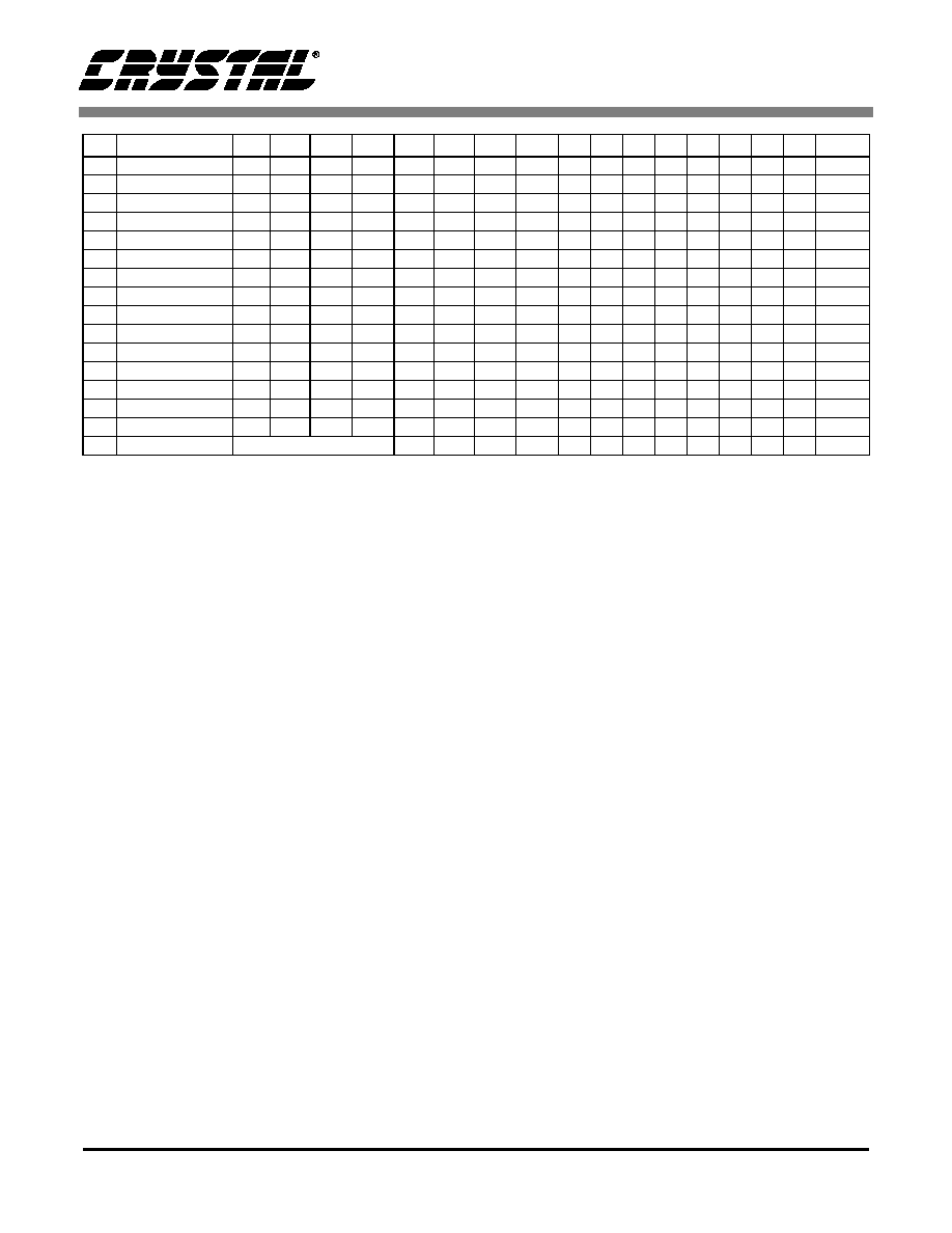
CS4205
26
DS489PP2
Reg Register Name
D15 D14
D13
D12
D11
D10
D9
D8
D7
D6
D5
D4
D3
D2
D1
D0 Default
00h
PCM Input Volume
Mute
0
GL5
GL4
GL3
GL2
GL1
GL0
0
0
GR5
GR4 GR3
GR2 GR1 GR0
8000h
01h
ADC Input Volume
Mute
0
GL5
GL4
GL3
GL2
GL1
GL0
0
0
GR5
GR4 GR3
GR2 GR1 GR0
8000h
02h
SDI1 Volume
Mute
0
GL5
GL4
GL3
GL2
GL1
GL0
0
0
GR5
GR4 GR3
GR2 GR1 GR0
8000h
03h
SDI2 Volume
Mute
0
GL5
GL4
GL3
GL2
GL1
GL0
0
0
GR5
GR4 GR3
GR2 GR1 GR0
8000h
04h
SDI3 Volume
Mute
0
GL5
GL4
GL3
GL2
GL1
GL0
0
0
GR5
GR4 GR3
GR2 GR1 GR0
8000h
05h
ZV Volume
Mute
0
GL5
GL4
GL3
GL2
GL1
GL0
0
0
GR5
GR4 GR3
GR2 GR1 GR0
8000h
06h
SDOUT Volume
Mute
0
GL5
GL4
GL3
GL2
GL1
GL0
0
0
GR5
GR4 GR3
GR2 GR1 GR0
8000h
07h
SDO2 Volume
Mute
0
GL5
GL4
GL3
GL2
GL1
GL0
0
0
GR5
GR4 GR3
GR2 GR1 GR0
8000h
08h
SP Engine Control
Res
SDI1M SRZC1 SRZC0 LPFS1 LPFS0 HPFS1 HPFS0 GL3
GL2
GL1
GL0
GR3
GR2 GR1 GR0
1800h
09h
IEC Config
EROF ELOF
MROF
MLOF
0
AMOR AROR
ALOR
0
0
0
0
0
0
0
0
0000h
0Ah
IEC Wakeup
EROF ELOF
MROF
MLOF
0
AMOR AROR
ALOR
0
0
0
0
0
0
0
0
0000h
0Bh
IEC Status
EROF ELOF
MROF
MLOF
0
AMOR AROR
ALOR
0
0
0
0
0
0
0
0
0000h
0Ch
BDI Config
E15
E14
E13
E12
E11
E10
E9
E8
E7
E6
E5
E4
E3
E2
E1
E0
0000h
0Dh
BDI Wakeup
E15
E14
E13
E12
E11
E10
E9
E8
E7
E6
E5
E4
E3
E2
E1
E0
0000h
0Eh
ZV Port Ctrl/Stat 1
ZVEN LOCK
0
Ph24
Ph23
Ph22
Ph21
Ph20
Ph19 Ph18 Ph17 Ph16 Ph15 Ph14 Ph13 Ph12
0000h
0Fh
ZV Port Ctrl/Stat 2
Reserved
Ph11
Ph10
Ph9
Ph8
Ph7
Ph6
Ph5
Ph4
Ph3
Ph2
Ph1
Ph0
0000h
Table 3. Indirectly Addressed Register Overview
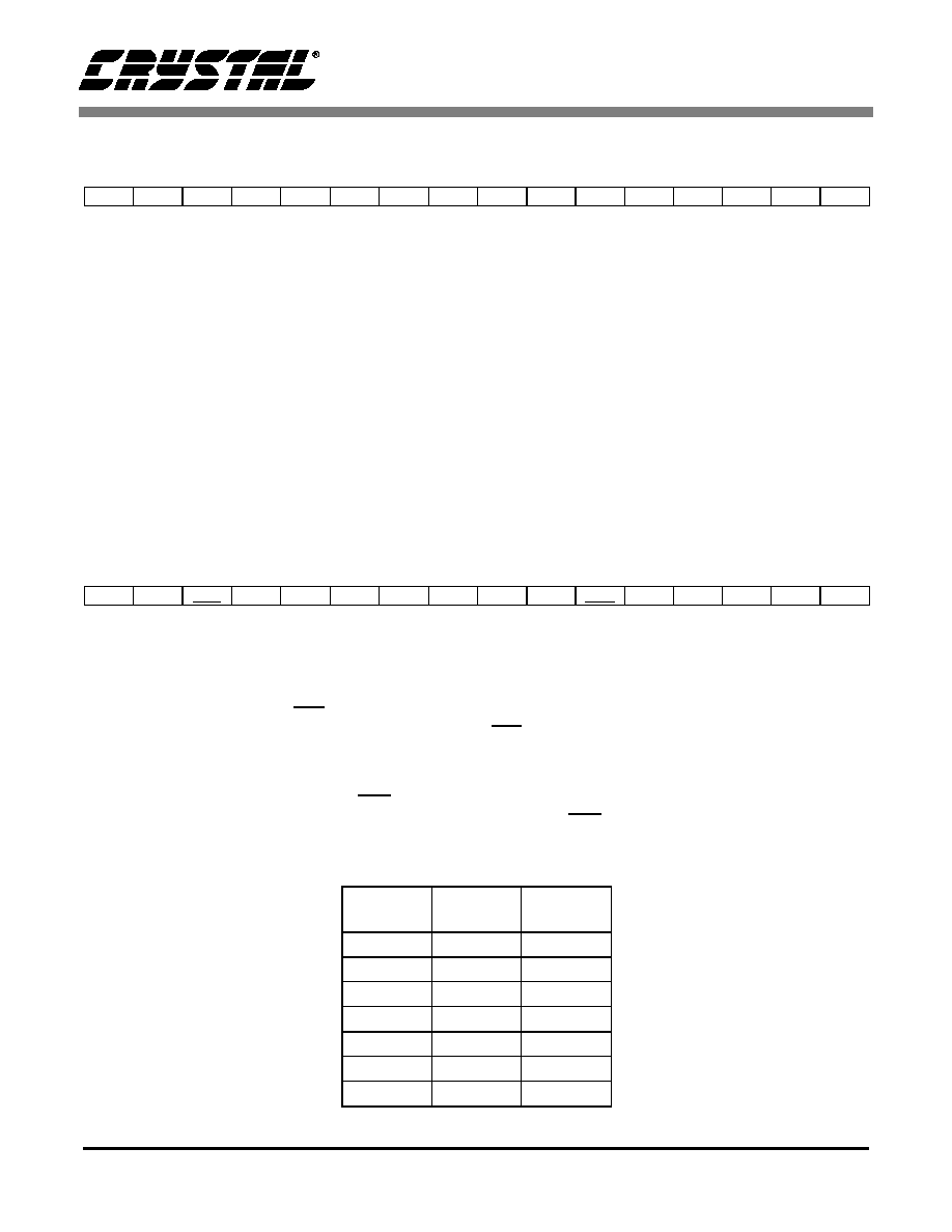
CS4205
DS489PP2
27
5.1
Reset Register (Index 00h)
SE[4:0]
SRS 3D Stereo Enhancement. SE[4:0] = 01001, indicating this feature is present.
ID8
18-bit ADC Resolution. The ID8 bit is `set', indicating this feature is present.
ID7
20-bit DAC resolution. The ID7 bit is `set', indicating this feature is present.
ID5
Loudness. The ID5 bit is `set', indicating this feature is present.
ID3
Simulated Stereo. The ID3 bit is `set', indicating this feature is present.
ID2
Bass & Treble. The ID2 bit is `set', indicating this feature is present.
ID0
Dedicated Mic PCM in Channel. The ID0 bit is `set', indicating this feature is present.
Default
Table 12 on page 37
h. The data in this register is read-only data.
Any write to this register causes a Register Reset of the audio control (Index 00h - 3Ah) and Cirrus Logic defined
(Index 5Ah - 7Ah) registers. A read from this register returns configuration information about the CS4205.
5.2
Master Volume Register (Index 02h)
Mute
Master Mute. Setting this bit mutes the LINE_OUT_L/R output signals.
ML[5:0]
Master Volume Left. These bits control the left master output volume. Each step corresponds
to 1.5 dB gain adjustment, with a total available range from 0 dB to -46.5 dB attenuation. Set-
ting the ML5 bit sets the left channel attenuation to -46.5 dB by forcing ML[4:0] to a `1' state.
ML[5:0] will read back 011111 when ML5 has been `set'. See Table 4 for further details.
MR[5:0]
Master Volume Right. These bits control the right master output volume. Each step corre-
sponds to 1.5 dB gain adjustment, with a total available range from 0 dB to -46.5 dB attenu-
ation. Setting the MR5 bit sets the right channel attenuation to -46.5 dB by forcing MR[4:0] to
a `1' state. MR[5:0] will read back 011111 when MR5 has been `set'. See Table 4 for further
details.
Default
8000h. This value corresponds to 0 dB attenuation and Mute `set'.
D15
D14
D13
D12
D11
D10
D9
D8
D7
D6
D5
D4
D3
D2
D1
D0
0
SE4
SE3
SE2
SE1
SE0
0
ID8
ID7
0
ID5
0
ID3
ID2
0
ID0
D15
D14
D13
D12
D11
D10
D9
D8
D7
D6
D5
D4
D3
D2
D1
D0
Mute
0
ML5
ML4
ML3
ML2
ML1
ML0
0
0
MR5
MR4
MR3
MR2
MR1
MR0
Mx5..Mx0
Write
Mx5..Mx0
Read
Gain
Level
000000
000000
0 dB
000001
000001
-1.5 dB
...
...
...
011111
011111
-46.5 dB
100000
011111
-46.5 dB
...
...
...
111111
011111
-46.5 dB
Table 4. Analog Mixer Output Attenuation

CS4205
28
DS489PP2
5.3
Mono Volume Register (Index 06h)
Mute
Mono Mute. Setting this bit mutes the MONO_OUT output signal.
MM[5:0]
Mono Volume Control. The MM[5:0] bits control the mono output volume. Each step corre-
sponds to 1.5 dB gain adjustment, with a total available range from 0 dB to -46.5 dB attenu-
ation. Setting the MM5 bit sets the mono attenuation to -46.5 dB by forcing MM[4:0] to a `1'
state. MM[5:0] will read back 011111 when MM5 has been `set'. See Table 4 on page 27 for
further attenuation levels.
Default
8000h. This value corresponds to 0 dB attenuation and Mute `set'.
5.4
Master Tone Control Register (Index 08h)
BA[3:0]
Bass Control. The BA[3:0] bits are used to control the bass gain in the effects engine. Each
step corresponds to 1.5 dB gain adjustment, with a total available range from +10.5 dB to
-10.5 dB gain. See Table 5 for further details. The center frequency from which the gain is
measured defaults to 100 Hz for bass, and may be changed using the LPFS[1:0] bits in the
Signal Processing Engine Control Register (Index 6Eh, Address 08h).
TR[3:0]
Treble Control. The TR[3:0] bits are used to control the treble gain in the effects engine. Each
step corresponds to 1.5 dB gain adjustment, with a total available range from +10.5 dB to
-10.5 dB gain. See Table 5 for further details. The center frequency from which the gain is
measured defaults to 10 kHz for treble, and may be changed using the HPFS[1:0] bits in the
Signal Processing Engine Control Register (Index 6Eh, Address 08h).
Default
0F0Fh. This value corresponds to bypass of bass and treble gain.
D15
D14
D13
D12
D11
D10
D9
D8
D7
D6
D5
D4
D3
D2
D1
D0
Mute
0
0
0
0
0
0
0
0
0
MM5
MM4
MM3
MM2
MM1
MM0
D15
D14
D13
D12
D11
D10
D9
D8
D7
D6
D5
D4
D3
D2
D1
D0
0
0
0
0
BA3
BA2
BA1
BA0
0
0
0
0
TR3
TR2
TR1
TR0
TR3..TR0
BA3..BA0
Gain
Level
0000
+10.5 dB
0001
+9 dB
...
...
0110
+1.5 dB
0111
0 dB
1000
-1.5 dB
...
...
1101
-9 dB
1110
-10.5 dB
1111
bypass
Table 5. Tone Control Values

CS4205
DS489PP2
29
5.5
PC_BEEP Volume Register (Index 0Ah)
Mute
PC_BEEP Mute. Setting this bit mutes the PC_BEEP input signal.
PV[3:0]
PC_BEEP Volume Control. The PV[3:0] bits control the gain levels of the PC_BEEP input
source to the Input Mixer. Each step corresponds to 3 dB gain adjustment, with 0000 = 0 dB.
The total range is 0 dB to -45 dB attenuation.
Default
0000h. This value corresponds to 0 dB attenuation and Mute `clear'.
This register has no effect on the PC_BEEP volume during RESET#.
5.6
Phone Volume Register (Index 0Ch)
Mute
Phone Mute. Setting this bit mutes the Phone input signal.
GN[5:0]
Phone Volume Control. The GN[4:0] bits control the gain level of the Phone input source to
the Input Mixer. Each step corresponds to 1.5 dB gain adjustment, with 01000 = 0 dB. The
total range is +12 dB to -34.5 dB attenuation. See Table 7 on page 31 for further attenuation
levels.
Default
8008h. This value corresponds to 0 dB attenuation and Mute `set'.
D15
D14
D13
D12
D11
D10
D9
D8
D7
D6
D5
D4
D3
D2
D1
D0
Mute
0
0
0
0
0
0
0
0
0
0
PV3
PV2
PV1
PV0
0
D15
D14
D13
D12
D11
D10
D9
D8
D7
D6
D5
D4
D3
D2
D1
D0
Mute
0
0
0
0
0
0
0
0
0
0
GN4
GN3
GN2
GN1
GN0

CS4205
30
DS489PP2
5.7
Microphone Volume Register (Index 0Eh)
Mute
Microphone Mute. Setting this bit mutes the MIC1 or MIC2 signal. The selection of the MIC1
or MIC2 input pin is controlled by the MS bit in the General Purpose Register (Index 20h).
20dB
Microphone 20 dB Boost. When `set', the 20dB bit enables the +20 dB microphone boost
block. In combination with the 10dB boost bit in the Misc. Crystal Control Register (Index 60h)
this bit allows for variable boost from 0 dB to +30 dB in steps of 10 dB. Table 6 summarizes
this behavior.
GN[4:0]
Microphone Volume Control. The GN[4:0] bits are used to control the gain level of the Micro-
phone input source to the Input Mixer. Each step corresponds to 1.5 dB gain adjustment, with
01000 = 0 dB. The total range is +12 dB to -34.5 dB gain. See Table 6 for further details.
Default
8008h. This value corresponds to 0 dB gain and Mute `set'.
D15
D14
D13
D12
D11
D10
D9
D8
D7
D6
D5
D4
D3
D2
D1
D0
Mute
0
0
0
0
0
0
0
0
20dB
0
GN4
GN3
GN2
GN1
GN0
GN4 - GN0
Gain Level
10dB = 0,
20dB = 0
10dB = 1,
20dB = 0
10dB = 0,
20dB = 1
10dB = 1,
20dB = 1
00000
+12.0 dB
+22.0 dB
+32.0 dB
+42.0 dB
00001
+10.5 dB
+20.5 dB
+30.5 dB
+40.5 dB
...
...
...
...
...
00111
+1.5 dB
+11.5 dB
+21.5 dB
+31.5 dB
01000
0.0 dB
+10.0 dB
+20.0 dB
+30.0 dB
01001
-1.5 dB
+8.5 dB
+18.5 dB
+28.5 dB
...
...
...
...
...
11111
-34.5 dB
-24.5 dB
-14.5 dB
-4.5 dB
Table 6. Microphone Input Gain Values
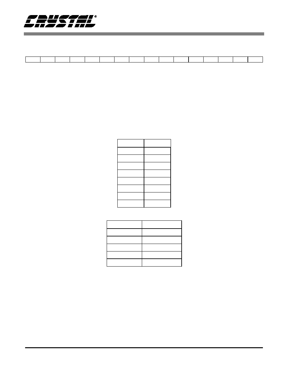
CS4205
DS489PP2
31
5.8
Analog Mixer Input Gain Registers (Index 10h - 18h)
Mute
Stereo Input Mute. Setting this bit mutes the respective input signal, both right and left inputs.
GL[4:0]
Left Volume Control. The GL[4:0] bits are used to control the gain level of the left analog input
source to the Input Mixer. Each step corresponds to 1.5 dB gain adjustment, with
01000 = 0 dB. The total range is +12 dB to -34.5 dB gain. See Table 7 for further details.
GR[4:0]
Right Volume Control. The GR[4:0] bits are used to control the gain level of the right analog
input source to the Input Mixer. Each step corresponds to 1.5 dB gain adjustment, with
01000 = 0 dB. The total range is +12 dB to -34.5 dB gain. See Table 7 for further details.
Default
8808h. This value corresponds to 0 dB gain and Mute `set'.
The Analog Mixer Input Gain Registers are listed in Table 8.
D15
D14
D13
D12
D11
D10
D9
D8
D7
D6
D5
D4
D3
D2
D1
D0
Mute
0
0
GL4
GL3
GL2
GL1
GL0
0
0
0
GR4
GR3
GR2
GR1
GR0
Gx4 - Gx0 Gain Level
00000
+12.0 dB
00001
+10.5 dB
...
...
00111
+1.5 dB
01000
0.0 dB
01001
-1.5 dB
...
...
11111
-34.5 dB
Table 7. Analog Mixer Input Gain Values
Register Index
Function
10h
Line In Volume
12h
CD Volume
14h
Video Volume
16h
Aux Volume
18h
PCM Out Volume
Table 8. Analog Mixer Input Gain Register Index

CS4205
32
DS489PP2
5.9
Input Mux Select Register (Index 1Ah)
SL[2:0]
Left Channel Source. The SL[2:0] bits select the left channel source to pass to the ADCs for
recording. See Table 9 for possible values.
SR[2:0]
Right Channel Source. The SR[2:0] bits select the right channel source to pass to the ADCs
for recording. See Table 9 for possible values.
Default
0000h. This value selects the Mic input for both channels.
D15
D14
D13
D12
D11
D10
D9
D8
D7
D6
D5
D4
D3
D2
D1
D0
0
0
0
0
0
SL2
SL1
SL0
0
0
0
0
0
SR2
SR1
SR0
Sx2 - Sx0
Record Source
000
Mic
001
CD Input
010
Video Input
011
Aux Input
100
Line Input
101
Stereo Mix
110
Mono Mix
111
Phone Input
Table 9. Input Mux Selection

CS4205
DS489PP2
33
5.10
Record Gain Register (Index 1Ch)
Mute
Record Gain Mute. Setting this bit mutes the input to the L/R ADCs.
GL[3:0]
Left ADC Gain. The GL[3:0] bits control the input gain on the left channel of the analog
source, applied after the input mux and before the ADCs. Each step corresponds to 1.5 dB
gain adjustment, with 0000 = 0 dB. The total range is 0 dB to +22.5 dB gain. See Table 10 for
further details.
GR[3:0]
Right ADC Gain. The GR[3:0] bits control the input gain on the right channel of the analog
source, applied after the input mux and before the ADCs. Each step corresponds to 1.5 dB
gain adjustment, with 0000 = 0 dB. The total range is 0 dB to +22.5 dB gain.See Table 10 for
further details.
Default
8000h. This value corresponds to 0 dB gain and Mute `set'.
5.11
Record Gain Mic Register (Index 1Eh)
Mute
Mic Record Gain Mute. When `set', mutes the input to the microphone ADC.
GM[3:0]
Mic ADC gain. The GM[3:0] bits control the input gain on the microphone source. The gain is
applied after the input mux and before the ADC. Each step corresponds to 1.5 dB gain ad-
justment, with 0000 = 0 dB. The total range is 0 dB to +22.5 dB gain. See Table 10 for further
details.
Default
8000h. This value corresponds to 0 dB gain and Mute `set'.
D15
D14
D13
D12
D11
D10
D9
D8
D7
D6
D5
D4
D3
D2
D1
D0
Mute
0
0
0
GL3
GL2
GL1
GL0
0
0
0
0
GR3
GR2
GR1
GR0
Gx4 - Gx0 Gain Level
1111
+22.5 dB
...
...
0001
+1.5 dB
0000
0 dB
Table 10. Record Gain Values
D15
D14
D13
D12
D11
D10
D9
D8
D7
D6
D5
D4
D3
D2
D1
D0
Mute
0
0
0
0
0
0
0
0
0
0
0
GM3
GM2
GM1
GM0

CS4205
34
DS489PP2
5.12
General Purpose Register (Index 20h)
POP
PCM Out Path. When `clear', the PCM out path is mixed pre 3D. When `set', the PCM out path
is mixed post 3D.
ST
Stereo Enhancement Enable. When `set', the ST bit enables the simulated stereo enhance-
ment via the SRS Mono algorithm.
3D
3D Enable. When `set', the 3D bit enables the 3D stereo enhancement via the SRS Stereo
algorithm.
LD
Loudness Enable. When `set', the LD bit enables the loudness or "bass boost" via the equal-
izer algorithm.
MIX
Mono Output Path. This bit controls the source of the mono output driver. When `clear', the
output of the stereo-to-mono mixer is sent to the mono output. When `set', the output of the
microphone boost stage is sent to the mono output. The source of the stereo-to-mono mixer
is controlled by the TMM bit in the AC Mode Control Register (Index 5Eh). The source of the
microphone boost stage is controlled by the MS bit in the General Purpose Register
(Index 20h).
MS
Microphone Select. The MS bit determines which of the two Mic inputs are passed to the mix-
er. When `set', the MIC2 input is selected. When `clear', the MIC1 input is selected.
LPBK
Loopback Enable. When `set', the LPBK bit enables the ADC/DAC Loopback Mode. This bit
routes the output of the ADCs to the input of the DACs without involving the AC-link.
Default
0000h
5.13
3D Control Register (Index 22h)
CR[3:0]
Center Control. The CR[3:0] bits control the amount of the sum signal, (L+R), that is added
to the final left and right digital signals.
DP[3:0]
Depth Control. The DP[3:0] bits control the amount of processed difference signal, (L-R)
p
,
that is added to the final left and right digital signals.
Default
0000h. This value corresponds to -22.5 dB center and depth attenuation.
This register is used to control the center and depth of the SRS stereo enhancement function in the effects engine.
Each step corresponds to 1.5 dB gain adjustment, with a total available range from 0 dB to -22.5 dB attenuation.
The recommended starting point for listening is -12 dB center attenuation and -4.5 dB depth attenuation, a register
value of 070Ch.
D15
D14
D13
D12
D11
D10
D9
D8
D7
D6
D5
D4
D3
D2
D1
D0
POP
ST
3D
LD
0
0
MIX
MS
LPBK
0
0
0
0
0
0
0
D15
D14
D13
D12
D11
D10
D9
D8
D7
D6
D5
D4
D3
D2
D1
D0
0
0
0
0
CR3
CR2
CR1
CR0
0
0
0
0
DP3
DP2
DP1
DP0

CS4205
DS489PP2
35
5.14
Powerdown Control/Status Register (Index 26h)
EAPD
External Amplifier Power Down. The EAPD pin follows this bit and is generally used to power
down external amplifiers. The EAPD bit is mutually exclusive with the SDSC bit in the Serial
Port Control Register (Index 6Ah). The SDSC bit must be `clear' before the EAPD bit may be
`set'.
If the SDSC bit is `set', EAPD is a read-only bit and always returns `0'.
PR5
Internal Clock Disable. When `set', the internal master clock is disabled (BIT_CLK running).
The only way to recover from setting this bit is through a Cold Reset (driving the RESET# sig-
nal active).
PR4
AC-link Powerdown. When `set', the AC-link is powered down (BIT_CLK off). The AC-link can
be restarted through a Warm Reset using the SYNC signal, or a Cold Reset using the RE-
SET# signal (primary audio codec only).
PR3
Analog Mixer Powerdown (Vref off). When `set', the analog mixer and voltage reference are
powered down. When clearing this bit, the ANL, ADC, and DAC bits should be checked be-
fore writing any mixer registers.
PR2
Analog Mixer Powerdown (Vref on). When `set', the analog mixer is powered down (the volt-
age reference is still active). When clearing this bit, the ANL bit should be checked before writ-
ing any mixer registers.
PR1
Front DACs Powerdown. When `set', the DACs are powered down. When clearing this bit, the
DAC bit should be checked before sending any data to the DACs.
PR0
L/R ADCs and Input Mux Powerdown. When `set', the ADCs and the ADC input muxes are
powered down. When clearing this bit, no valid data will be sent down the AC-link until the
ADC bit goes high.
REF
Voltage Reference Ready Status. When `set', the REF bit indicates the voltage reference is
at a nominal level.
ANL
Analog Ready Status. When `set', the analog output mixer, input multiplexer, and volume con-
trols are ready. When `clear', no volume control registers should be written.
DAC
Front DAC Ready Status. When `set', the DACs are ready to receive data across the AC-link.
When `clear', the DACs will not accept any valid data.
ADC
L/R ADCs Ready Status. When `set', the ADCs are ready to send data across the AC-link.
When `clear', no data will be sent to the controller.
Default
0000h. This value indicates all blocks are powered on. The lower four bits will change as the
CS4205 finishes an initialization and calibration sequence.
The PR[5:0] and the EAPD bits are powerdown control for different sections of the CS4205 as well as external am-
plifiers. The REF, ANL, DAC, and ADC bits are read-only status bits which, when `set', indicate that a particular sec-
tion of the CS4205 is ready. After the controller receives the Codec Ready bit in input Slot 0, these status bits must
be checked before writing to any mixer registers. See Section 10, Power Management, for more information on the
powerdown functions.
D15
D14
D13
D12
D11
D10
D9
D8
D7
D6
D5
D4
D3
D2
D1
D0
EAPD
0
PR5
PR4
PR3
PR2
PR1
PR0
0
0
0
0
REF
ANL
DAC
ADC

CS4205
36
DS489PP2
5.15
Extended Audio ID Register (Index 28h)
ID[1:0]
Codec Configuration ID. These bits indicate the current codec configuration. When
ID[1:0] = 00, the CS4205 is the primary audio codec. When ID[1:0] = 01, 10, or 11, the
CS4205 is a secondary audio codec. The state of the ID[1:0] bits is determined at power-up
from the ID[1:0]# pins and the current clocking scheme, see Table 27 on page 63.
AMAP
Audio Slot Mapping. The AMAP bit indicates whether the optional AC '97 2.1 compliant
AC-link slot to audio DAC mapping is supported. This bit is a shadow of the AMAP bit in the
AC Mode Control Register (Index 5Eh). The PCM playback and capture slots are mapped ac-
cording to Table 14 on page 42.
VRM
Variable Rate Mic Audio. The VRM bit indicates whether variable rate Mic audio is supported.
This bit always returns `1', indicating that variable rate mic audio is available.
VRA
Variable Rate PCM Audio. The VRA bit indicates whether variable rate PCM audio is support-
ed. This bit always returns `1', indicating that variable rate PCM audio is available.
Default
x209h. The Extended Audio ID Register (Index 28h) is a read-only register.
5.16
Extended Audio Status/Control Register (Index 2Ah)
PRL
Mic ADC Powerdown. When `set', the PRL bit powers down the dedicated Mic ADC and cor-
responding input gain stage. To use the dedicated Mic ADC, clear the PRL bit first.
MADC
Mic ADC Ready Status. When `set', the MADC bit indicates the dedicated Mic ADC is ready
to transmit data.
VRM
Enable Variable Rate Mic Audio. When `set', the VRM bit allows access to the Mic ADC Rate
Register (Index 34h). This bit must be `set' in order to use variable mic capture rates. The
VRM bit also serves as a powerdown for the Mic ADC SRC block. Clearing VRM will reset the
Mic ADC Rate Register (Index 34h) to its default value and the SRC data path is flushed.
VRA
Enable Variable Rate Audio. When `set', the VRA bit allows access to the PCM Front DAC
Rate Register (Index 2Ch) and the PCM L/R ADC Rate Register (Index 32h). This bit must
be `set' in order to use variable PCM playback or capture rates. The VRA bit also serves as
a powerdown for the DAC and ADC SRC blocks. Clearing VRA will reset the PCM Front DAC
Rate Register (Index 2Ch) and the PCM L/R ADC Rate Register (Index 32h) to their default
values. The SRC data path is flushed and the Slot Request bits for the currently active DAC
slots will be fixed at `0'.
Default
4000h
D15
D14
D13
D12
D11
D10
D9
D8
D7
D6
D5
D4
D3
D2
D1
D0
ID1
ID0
0
0
0
0
AMAP
0
0
0
0
0
VRM
0
0
VRA
D15
D14
D13
D12
D11
D10
D9
D8
D7
D6
D5
D4
D3
D2
D1
D0
0
PRL
0
0
0
0
MADC
0
0
0
0
0
VRM
0
0
VRA
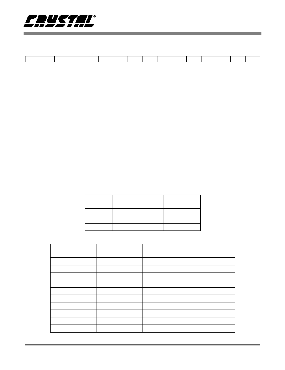
CS4205
DS489PP2
37
5.17
Audio Sample Rate Control Registers (Index 2Ch - 34h)
SR[15:0]
Sample Rate Select. The Audio Sample Rate Control Registers (Index 2Ch - 34h) control
playback and capture sample rates. The PCM Front DAC Rate Register (Index 2Ch) controls
the Front Left and Front Right DAC sample rates. The PCM L/R ADC Rate Register
(Index 32h) controls the Left and Right ADC sample rates. The Mic ADC Rate Register (Index
34h) controls the Microphone ADC sample rate.There are ten sample rates directly supported
by this register, shown in Table 12. Any value written to this register not contained inTable 12
is not directly supported and will be decoded according to the ranges indicated in the table.
The range boundaries have been chosen so that only bits SR[15:11] of each register will have
to be considered. All register read transactions will reflect the actual value stored (column 2
in Table 12) and not the one attempted to be written.
Default
BB80h. This value corresponds to 48 kHz sample rate.
Writes to the PCM Front DAC Rate Register (Index 2Ch) and the PCM L/R ADC Rate Register (Index 32h) are only
available in Variable Rate PCM Audio mode when the VRA bit in the Extended Audio Status/Control Register
(Index 2Ah) is `set'. If VRA = 0, writes to the register are ignored and the register will always read BB80h. Writes to
the Mic ADC Rate Register (Index 34h) are only available in Variable Rate Mic Audio mode when the VRM bit in the
Extended Audio Status/Control Register (Index 2Ah) is `set'. If VRM = 0, writes to the register are ignored and the
register will always read BB80h. Table 11 lists the SRC registers and their corresponding SRC enable bit.
D15
D14
D13
D12
D11
D10
D9
D8
D7
D6
D5
D4
D3
D2
D1
D0
SR15
SR14
SR13
SR12
SR11
SR10
SR9
SR8
SR7
SR6
SR5
SR4
SR3
SR2
SR1
SR0
Register
Index
SRC
SRC Enable Bit
(Index 2Ah)
2Ch
PCM Front DAC Rate
VRA
32h
PCM L/R ADC Rate
VRA
34h
Mic ADC Rate
VRM
Table 11. Audio Sample Rate Control Register Index
Sample Rate
(Hz)
SR[15:0], register
content (hex value)
SR[15:0], decode
range (hex value)
SR[15:11], decode
range (bin value)
8,000
1F40
0000 - 1FFF
00000 - 00011
9,600
2580
2000 - 27FF
00100 - 00100
11,025
2B11
2800 - 2FFF
00101 - 00101
13,714
3592
3000 - 37FF
00110 - 00110
16,000
3E80
3800 - 47FF
00111 - 01000
22,050
5622
4800 - 57FF
01001 - 01010
24,000
5DC0
5800 - 6FFF
01011 - 01101
32,000
7D00
7000 - 8FFF
01110 - 10001
44,100
AC44
9000 - AFFF
10010 - 10101
48,000
BB80
B000 - FFFF
10110 - 11111
Table 12. Directly Supported SRC Sample Rates for the CS4205

CS4205
38
DS489PP2
5.18
Extended Modem ID Register (Index 3Ch)
ID[1:0]
Codec Configuration ID. Primary is 00; Secondary is 01,10,or 11. This is a reflection of the
ID[1:0]# configuration pins. The state of the ID[1:0] bits is determined at power-up from the
Codec ID[1:0]# pins and the current clocking scheme, see Table 27 on page 63.
Default
x000h. This value indicates no supported modem functions.
The Extended Modem ID Register (Index 3Ch) is a read/write register that identifies the CS4205 modem capabilities.
Writing any value to this location issues a reset to modem registers (Index 3Ch-54h), including GPIO registers
(Index 4Ch - 54h). Audio registers are not reset by a write to this location.
5.19
Extended Modem Status/Control Register (Index 3Eh)
PRA
GPIO Powerdown. When `set', the PRA bit powers down the GPIO subsystem. When the
GPIO section is powered down, all outputs must be tri-stated and input Slot 12 should be
marked invalid when the AC-link is active. To use any GPIO functionality, including Internal
Error Signaling, PRA must be cleared first.
GPIO
GPIO. When `set', the GPIO bit indicates the GPIO subsystem is ready for use. When `set',
input Slot 12 will also be marked valid.
Default
0100h
5.20
GPIO Pin Configuration Register (Index 4Ch)
GC[4:0]
GPIO Pin Configuration. When `set', the GC[4:0] bits define the corresponding GPIO pin as
an input. When `clear', the corresponding GPIO pin is defined as an output. When the SDEN
bit in the Serial Port Control Register (Index 6Ah) is `set', the GC[1:0] bits are read-only bits
and always return `0'. When SDEN is `clear', the GC[1:0] bits function normally. Likewise,
GC2 depends on SDI1, GC3 depends on SDI2, and GC4 depends on SDI3. The SDI[1:3] bits
are located in the Serial Port Control Register (Index 6Ah).
Default
001Fh. This value corresponds to all GPIO pins configured as inputs.
After a Cold Reset or a modem Register Reset (see Extended Modem ID Register (Index 3Ch)), all GPIO pins are
configured as inputs. The upper 11 bits of this register always return `0'.
D15
D14
D13
D12
D11
D10
D9
D8
D7
D6
D5
D4
D3
D2
D1
D0
ID1
ID0
0
0
0
0
0
0
0
0
0
0
0
0
0
0
D15
D14
D13
D12
D11
D10
D9
D8
D7
D6
D5
D4
D3
D2
D1
D0
0
0
0
0
0
0
0
PRA
0
0
0
0
0
0
0
GPIO
D15
D14
D13
D12
D11
D10
D9
D8
D7
D6
D5
D4
D3
D2
D1
D0
0
0
0
0
0
0
0
0
0
0
0
GC4
GC3
GC2
GC1
GC0

CS4205
DS489PP2
39
5.21
GPIO Pin Polarity/Type Configuration Register (Index 4Eh)
GP[4:0]
GPIO Pin Configuration. This register defines the GPIO input polarity (0 = Active Low,
1 = Active High) when a GPIO pin is configured as an input. The GP[4:0] bits define the GPIO
output type (0 = CMOS, 1 = OPEN-DRAIN) when a GPIO pin is configured as an output. The
GC[4:0] bits in the GPIO Pin Configuration Register (Index 4Ch) define the GPIO pins as in-
puts or outputs. See Table 13 for the various GPIO configurations.
Default
FFFFh
After a Cold Reset or a modem Register Reset this register defaults to all 1's. The upper 11 bits of this register al-
ways return `1'.
5.22
GPIO Pin Sticky Register (Index 50h)
GS[4:0]
GPIO Pin Sticky. This register defines the GPIO input type (0 = not sticky, 1 = sticky) when a
GPIO pin is configured as an input. The GPIO pin status of an input configured as "sticky" is
`cleared' by writing a `0' to the corresponding bit of the GPIO Pin Status Register (Index 54h),
and by reset.
Default
0000h
After a Cold Reset or a modem Register Reset this register defaults to all 0's, specifying "non-sticky". "Sticky" is de-
fined as edge sensitive, "non-sticky" as level sensitive. The upper 11 bits of this register always return `0'.
D15
D14
D13
D12
D11
D10
D9
D8
D7
D6
D5
D4
D3
D2
D1
D0
1
1
1
1
1
1
1
1
1
1
1
GP4
GP3
GP2
GP1
GP0
GCx GPx Function
Configuration
0
0
Output
CMOS Drive
0
1
Output
Open Drain
1
0
Input
Active Low
1
1
Input
Active High (default)
Table 13. GPIO Input/Output Configurations
D15
D14
D13
D12
D11
D10
D9
D8
D7
D6
D5
D4
D3
D2
D1
D0
0
0
0
0
0
0
0
0
0
0
0
GS4
GS3
GS2
GS1
GS0

CS4205
40
DS489PP2
5.23
GPIO Pin Wakeup Mask Register (Index 52h)
GW[4:0]
GPIO Pin Wakeup. This register provides a mask for determining if an input GPIO change will
generate a wakeup event (0 = No, 1 = yes). When the AC-link is powered up, a wakeup event
will be communicated through the assertion of GPIO_INT = 1 in input Slot 12. When the
AC-link is powered down (Powerdown Control/Status Register (Index 26h) bit PR4 = 1 for pri-
mary codecs), a wakeup event will be communicated through a `0' to `1' transition on
SDATA_IN.
Default
0000h
GPIO bits which have been programmed as inputs, "sticky", and "wakeup", upon transition either (high-to-low) or
(low-to-high) depending on pin polarity, will cause an AC-link wakeup if and only if the AC-link was powered down.
Once the controller has re-established communication with the CS4205 following a Warm Reset, it will continue to
signal the wakeup event through the GPIO_INT bit of input Slot 12 until the AC '97 controller clears the inter-
rupt-causing bit in the GPIO Pin Status Register (Index 54h); or the "wakeup", config, or "sticky" status of that GPIO
pin changes.
After a Cold Reset or a modem Register Reset (see Extended Modem ID Register (Index 3Ch)) this register defaults
to all 0's, specifying no wakeup event. The upper 11 bits of this register always return `0'.
5.24
GPIO Pin Status Register (Index 54h)
GI[4:0]
GPIO Pin Status. This register reflects the state of all GPIO pin inputs and outputs. These
values are also reflected in Slot 12 of every SDATA_IN frame. GPIO inputs configured as
"sticky" are `cleared' by writing a `0' to the corresponding bit of this register. The GPIO_INT
bit in input Slot 12 is `cleared' by clearing all interrupt-causing bits in this register.
Default
0000h
GPIO pins which have been programmed as inputs and "sticky", upon transition either high-to-low or low-to-high de-
pending on pin polarity, will cause the individual GI bit to be `set', and remain `set' until `cleared'. GPIO pins which
have been programmed as outputs are controlled either through output Slot 12 or through this register, depending
on the state of the GPOC bit in the Misc. Crystal Control Register (Index 60h). If the GPOC bit is `cleared', the GI
bits in this register are read-only and reflect the status of the corresponding GPIO output pin `set' through output
slot 12. If the GPOC bit is `set', the GI bits in this register are read/write bits and control the corresponding GPIO
output pins.
The default value is always the state of the GPIO pin. The upper 11 bits of this register should be forced to zero in
this register and input Slot 12.
D15
D14
D13
D12
D11
D10
D9
D8
D7
D6
D5
D4
D3
D2
D1
D0
0
0
0
0
0
0
0
0
0
0
0
GW4
GW3
GW2
GW1
GW0
D15
D14
D13
D12
D11
D10
D9
D8
D7
D6
D5
D4
D3
D2
D1
D0
0
0
0
0
0
0
0
0
0
0
0
GI4
GI3
GI2
GI1
GI0

CS4205
DS489PP2
41
5.25
AC Mode Control Register (Index 5Eh)
DACS
DAC Source Select. The DACS bit controls the source of data routed to the DACs. If this bit
is `clear', the DACs will receive data from the DAC slots, see Table 14 for actual slots used.
If this bit is `set', the DACs will receive data from the CS4205 digital effects engine.
CAPS[1:0]
L/R Capture Source Select. The CAPS[1:0] bits control the source of data routed to the L/R
ADC slots, see Table 14 for actual slots used. Table 15 lists the available capture options. If
a reserved source is selected, the capture slot data will be fixed to `0'.
MICS
Microphone Capture Source Select. The MICS bit selects the source of data routed to the Mic
ADC slot. If this bit is `clear', the Mic capture slot will receive data from the Mic ADC. If this bit
is `set', the Mic capture slot will receive the left channel data from the first serial data input
port.
TMM
True Mono Mode. The TMM bit controls the source of the stereo-to-mono mixer that feeds
into the mono out select mux. If this bit is `clear', the output of the stereo input mixer is sent
to the stereo-to-mono mixer. If this bit is `set', the output of the DAC direct mode mux is sent
to the stereo-to-mono mixer. This allows a true mono mix that includes the PC Beep and
Phone inputs and also works during DAC direct mode.
DDM
DAC Direct Mode. The DDM bit controls the source of the line output drivers. When this bit is
`clear', the CS4205 stereo output mixer drives the line output. When this bit is `set', the
CS4205 audio DACs (DAC1 and DAC2) directly drive the line output.
AMAP
Audio Slot Mapping. The AMAP bit controls whether the CS4205 responds to the Codec ID
based slot mapping as outlined in the AC '97 2.1 Specification. This bit is shadowed in the
Extended Audio ID Register (Index 28h). Refer to Table 14 for the slot mapping configura-
tions.
SM[1:0]
Slot Map. The SM[1:0] bits define the Slot Mapping for the CS4205 when the AMAP bit is
`cleared'. Refer to Table 14 for the slot mapping configurations.
SDOS[1:0]
Serial Data Output Source Select. The SDOS[1:0] bits control the source of data routed to the
CS4205 first serial data output port. Table 15 on page 42 lists the available source options. If
a reserved source is selected, the serial output data will be fixed to `0'.
SPDS[1:0]
S/PDIF Transmitter Source Select. The SPDS[1:0] bits control the source of data routed to
the S/PDIF transmitter. Table 15 on page 42 lists the available source options.
Default
0080h
See Section 3, Digital Signal Paths, for more information on using the bits in this register to create various digital
signal path options.
D15
D14
D13
D12
D11
D10
D9
D8
D7
D6
D5
D4
D3
D2
D1
D0
DACS CAPS1 CAPS0 MICS
0
0
TMM
DDM
AMAP
0
SM1
SM0
SDOS1 SDOS0 SPDS1 SPDS0

CS4205
42
DS489PP2
Slot
Assignment
Mode
Codec ID
Slot Map
AMAP
Slot Assignments
ID1
ID0 SM1 SM0
DAC
SDOUT
SDO2
ADC
SPDIF for
SPDS = 00
SPDIF for
SPDS = 01
L
R
L
R
L
R
L
R
M
AMAP Mode 0
0
0
X
X
1
3
4
7
8
6
9
3
4
6
AMAP Mode 1
0
1
X
X
1
3
4
7
8
6
9
3
4
6
AMAP Mode 2
1
0
X
X
1
7
8
6
9
10
11
7
8
6
AMAP Mode 3
1
1
X
X
1
6
9
7
8
10
11
7
8
6
Slot Map Mode 0
X
X
0
0
0
3
4
7
8
6
9
3
4
6
Slot Map Mode 1
X
X
0
1
0
7
8
6
9
10
11
7
8
6
Slot Map Mode 2
X
X
1
0
0
6
9
7
8
10
11
7
8
6
Slot Map Mode 3
X
X
1
1
0
5
11
7
8
6
9
5
11
6
Table 14. Slot Mapping for the CS4205
CAPS[1:0],
SDOS[1:0],
or
SPDS[1:0]
L/R Capture
Source
(CAPS[1:0])
Serial Data
Output
Source
(SDOS[1:0])
S/PDIF
Transmitter
Source
(SPDS[1:0])
00
L/R ADCs
SDOUT slots
DAC slots
01
reserved
reserved
SDO2 slots
10
Digital Mixer
Digital Mixer
Digital Mixer
11
Digital Effects
Digital Effects
Digital Effects
Table 15. Digital Signal Source Selects

CS4205
DS489PP2
43
5.26
Misc. Crystal Control Register (Index 60h)
DPC
DAC Phase Control. This bit controls the phase of the PCM stream sent to the DACs (after
SRC). When `cleared' the phase of the signal will remain unchanged. When this bit is `set',
each PCM sample will be inverted before being sent to the DACs.
10dB
Microphone 10 dB Boost. When `set', the 10dB bit enables an additional boost of 10 dB on
the selected microphone input. In combination with the 20dB boost bit in the Microphone Vol-
ume Register (Index 0Eh) this bit allows for variable boost from 0 dB to +30 dB in steps of
10 dB.
CRST
Force Cold Reset. The CRST bit is used as an override to the New Warm Reset behavior
defined during PR4 powerdown. If this bit is `set', an active RESET# signal will force a Cold
Reset to the CS4205 during a PR4 powerdown.
GPOC
General Purpose Output Control. The GPOC bit specifies the mechanism by which the status
of a General Purpose Output pin can be controlled. If this bit is `cleared', the GPO status is
controlled through the standard AC '97 method of setting the appropriate bits in output
Slot 12. If this bit is `set', the GPO status is controlled through the GPIO Pin Status Register
(Index 54h).
LOSM
Loss of SYNC Mute Enable. The LOSM bit controls the loss of SYNC mute function. If this bit
is `set', the CS4205 will mute all analog outputs for the duration of loss of SYNC. If this bit is
`cleared', the mixer will continue to function normally during loss of SYNC. The CS4205 ex-
pects to sample SYNC `high' for 16 consecutive BIT_CLK periods and then `low' for 240 con-
secutive BIT_CLK periods, otherwise loss of SYNC becomes true.
Default
0002h
D15
D14
D13
D12
D11
D10
D9
D8
D7
D6
D5
D4
D3
D2
D1
D0
0
0
0
DPC
0
0
Reserved
10dB
CRST
Reserved
GPOC
Reserved
LOSM

CS4205
44
DS489PP2
5.27
S/PDIF Control Register (Index 68h)
SPEN
S/PDIF Enable. The SPEN bit enables S/PDIF data transmission on the SPDO/SDO2 pin.
The SPEN bit routes the left and right channel data from the AC '97 controller, the digital mix-
er, or the digital effects engine to the S/PDIF transmitter block. The actual data routed to the
S/PDIF block is controlled through the SPDS[1:0]/AMAP/SM[1:0] configuration in the AC
Mode Control Register (Index 5Eh). This bit can only be `set' if the SDO2 bit in the Serial Port
Control Register (Index 6Ah) is `0'. If the SDO2 bit is `set', SPEN is a read-only bit and always
returns `0'.
Val
Validity. The Val bit is mapped to the V bit (bit 28) of every sub-frame. If this bit is `clear', the
signal is suitable for conversion or processing.
Fs
Sample Rate. The Fs bit indicates the sampling rate for the S/PDIF data. The inverse of this
bit is mapped to bit 25 of the channel status block. When the Fs bit is `clear', the sampling
frequency is 48 kHz. When `set', the sampling frequency is 44.1 kHz. The actual rate at which
S/PDIF data are being transmitted solely depends on the master clock frequency of the
CS4205. The Fs bit is merely an indicator to the S/PDIF receiver.
L
Generation Status. The L bit is mapped to bit 15 of the channel status block. For category
codes 001xxxx, 0111xxx and 100xxxx, a value of `0' indicates original material and a value of
`1' indicates a copy of original material. For all other category codes the definition of the L bit
is reversed.
CC[6:0]
Category Code. The CC[6:0] bits are mapped to bits 8-14 of the channel status block.
Emph
Data Emphasis. The Emph bit is mapped to bit 3 of the channel status block. When `set',
50/15us filter pre-emphasis is indicated. When is `clear', no pre-emphasis is indicated.
Copy
Copyright. The Copy bit is mapped to bit 2 of the channel status block. If the Copy bit is `set'
copyright is not asserted and copying is permitted.
/Audio
Audio / Non-Audio. The /Audio bit is mapped to bit 1 of the channel status block. If the /Audio
bit is `clear', the data transmitted over S/PDIF is assumed to be digital audio. If the /Audio bit
is `set', non-audio data is assumed.
Pro
Professional/Consumer. The Pro bit is mapped to bit 0 of the channel status block. If the Pro
bit is `clear', consumer use of the audio control block is indicated. If the bit is `set', professional
use is indicated.
Default
0000h
For a further discussion of the proper use of the channel status bits see application note AN22: Overview of Digital
Audio Interface Data Structures [3].
D15
D14
D13
D12
D11
D10
D9
D8
D7
D6
D5
D4
D3
D2
D1
D0
SPEN
Val
0
Fs
L
CC6
CC5
CC4
CC3
CC2
CC1
CC0
Emph
Copy /Audio
Pro

CS4205
DS489PP2
45
5.28
Serial Port Control Register (Index 6Ah)
SDEN
Serial Data Output Enable. The SDEN bit enables transmission of serial data on the SDOUT
pin. The SDEN bit routes the left and right channel data from the AC '97 controller, the digital
mixer, or the digital effects engine to the serial data port. The actual data routed to the serial
data port is controlled through the SDOS[1:0]/AMAP/SM[1:0] configuration in the AC Mode
Control Register (Index 5Eh). SDEN also functions as a master control for the serial data input
ports, the second serial data output port and the serial clock. Setting this bit also disables the
GPIO[1:0] pins and clears the GC[1:0] bits in the GPIO Pin Configuration Register
(Index 4Ch). Clearing this bit re-enables the GPIO[1:0] pins and sets the GC[1:0] bits.
SDI[3:1]
Serial Data Input Enable. The SDI[3:1] bits individually enable the reception of serial data on
the SDI[3:1] pins. Each of these bits routes the left and right channel data from the corre-
sponding serial data input port to its associated volume control. These bits can only be set if
the SDEN bit is `1' and will be cleared automatically if SDEN returns to `0'. If the SDEN bit is
`0', SDI[3:1] are read-only bits and always return `0'. If allowed, setting one of these bits also
disables the corresponding GPIO pin and clears the associated GC bit for this pin in the GPIO
Pin Configuration Register (Index 4Ch). Clearing one of these bits re-enables the correspond-
ing GPIO pin and sets the associated GC bit.
SDO2
Serial Data Output 2 Enable. The SDO2 bit enables transmission of serial data on the
SPDO/SDO2 pin. The SDO2 bit routes the left and right channel data from the AC '97 con-
troller to the second serial data port. The actual slots routed to the second serial data port are
controlled through the AMAP/SM[1:0] configuration in the AC Mode Control Register (Index
5Eh). This bit can only be `set' if the SDEN bit is `1' and will be `cleared' automatically if SDEN
returns to `0'. Furthermore, the SDO2 bit can only be `set' if the SPEN bit in the S/PDIF Control
Register (Index 68h) is `0'. If the SDEN bit is `0' or the SPEN bit is `1', SDO2 is a read-only bit
and always returns `0'.
SDSC
Serial Clock Enable. The SDSC bit enables transmission of a serial clock on the EAPD/SCLK
pin. Serial data can be routed to DACs that support internal SCLK mode without transmitting
a serial clock. For DACs that only support external SCLK mode, transmission of a serial clock
is required and this bit must be set to `1'. This bit can only be set if the SDEN bit is `1' and will
be cleared automatically if SDEN returns to `0'. Furthermore, the SDSC bit can only be `set'
if the EAPD bit in the Powerdown Control/Status Register (Index 26h) is `0'. If the SDEN bit
is `0' or the EAPD bit is `1', SDSC is a read-only bit and always returns `0'.
SDF[1:0]
Serial Data Format. The SDF[1:0] bits control the format of the serial data transmitted on the
two output ports and the three input ports. All ports will use the same format. See Table 16
for available formats.
Default
0000h
D15
D14
D13
D12
D11
D10
D9
D8
D7
D6
D5
D4
D3
D2
D1
D0
SDEN
0
0
0
0
0
0
0
0
SDI3
SDI2
SDI1
SDO2 SDSC SDF1
SDF0
SDF1 SDF0
Serial Data Format
0
0
I
2
S
0
1
Left Justified
1
0
Right Justified, 20-bit data
1
1
Right Justified, 16-bit data
Table 16. Serial Data Format Selection
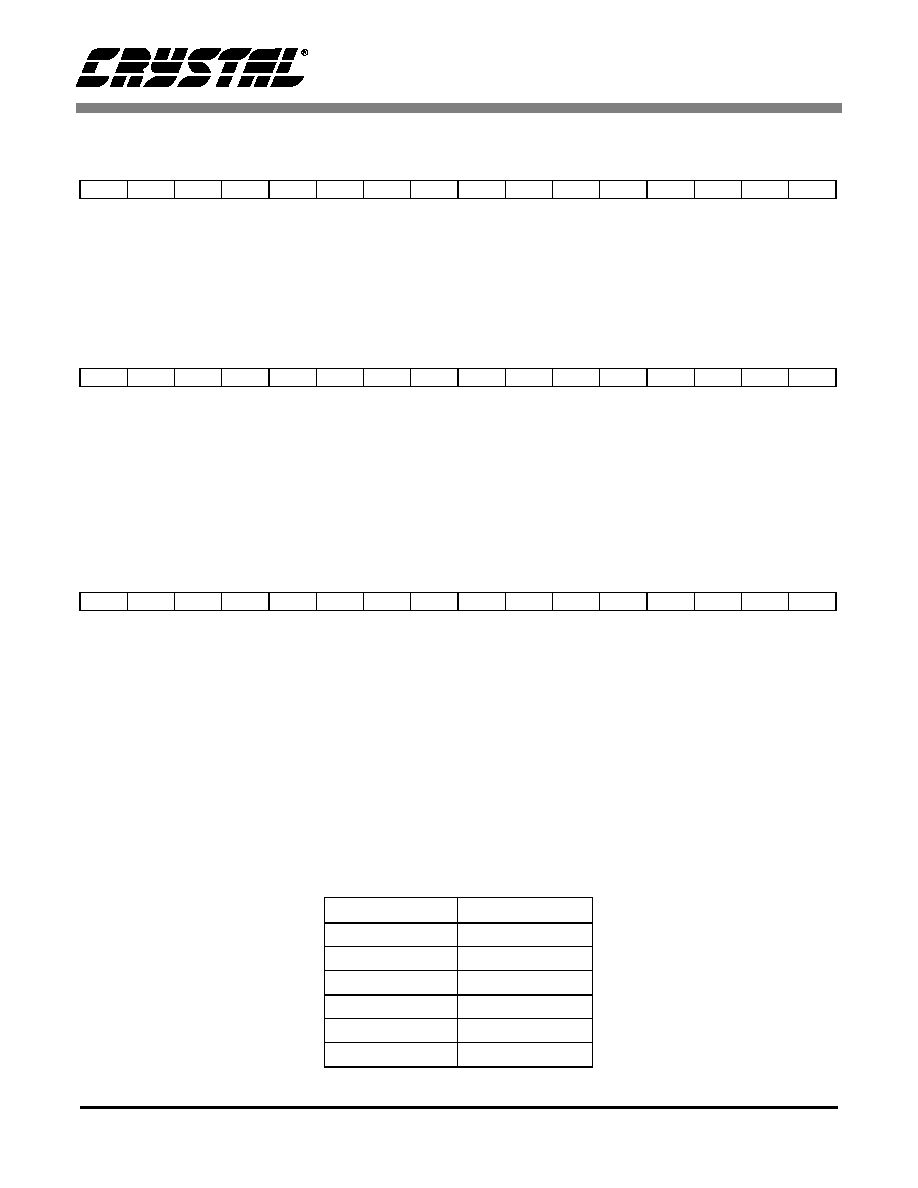
CS4205
46
DS489PP2
5.29
Special Feature Address Register (Index 6Ch)
A[3:0]
Special Feature Address. This register functions as an index register to select the desired
functionality of the Special Feature Data Register (Index 6Eh). Before using any of these in-
dexed registers, the correct index value must be written to bits A[3:0].
Default
0000h
5.30
Special Feature Data Register (Index 6Eh)
D[15:0]
Special Feature Data. This register is an indexed data port for the special feature registers
(Index 6E, Address 00h - 0Fh) which control advanced subsystems of the CS4205, such as
digital mixer settings, effects engine parameters, ZV Port control, and internal error condition
signaling. Before using any of these functions, the correct index value must be written to the
Special Feature Address Register (Index 6Ch).
Default
8000h
5.31
Digital Mixer Input Volume Registers (Index 6Eh, Address 00h - 05h)
Mute
Digital Mixer Mute. Setting this bit mutes the respective input signal, both left and right inputs.
GL[5:0]
Left Volume Control. The GL[5:0] bits are used to control the digital mixer left channel input
volume. Each step corresponds to 1 dB gain adjustment. The total range is 0 dB to -63 dB
gain.
GR[5:0]
Right Volume Control. The GR[4:0] bits are used to control the digital mixer right channel in-
put volume. Each step corresponds to 1 dB gain adjustment. The total range is 0 dB to -63 dB
gain.
Default
8000h. This value corresponds to 0 dB gain and Mute `set'.
If the digital mixer signals an overflow condition by setting the MLOF or MROF bit in the IEC Status Register
(Index 6Eh, Address 0Bh), the controller should correct the error by reducing the digital mixer input volumes in these
registers. The Digital Mixer Input Volume Registers are listed in Table 17.
D15
D14
D13
D12
D11
D10
D9
D8
D7
D6
D5
D4
D3
D2
D1
D0
0
0
0
0
0
0
0
0
0
0
0
0
A3
A2
A1
A0
D15
D14
D13
D12
D11
D10
D9
D8
D7
D6
D5
D4
D3
D2
D1
D0
D15
D14
D13
D12
D11
D10
D9
D8
D7
D6
D5
D4
D3
D2
D1
D0
D15
D14
D13
D12
D11
D10
D9
D8
D7
D6
D5
D4
D3
D2
D1
D0
Mute
0
GL5
GL4
GL3
GL2
GL1
GL0
0
0
GR5
GR4
GR3
GR2
GR1
GR0
Register Address
Function
00h
PCM Input Volume
01h
ADC Input Volume
02h
SDI1 Volume
03h
SDI2 Volume
04h
SDI3 Volume
05h
ZV Volume
Table 17. Digital Mixer Input Volume Register Index

CS4205
DS489PP2
47
5.32
Serial Data Port Volume Control Registers (Index 6Eh, Address 06h - 07h)
Mute
Serial Data Port Mute. Setting this bit mutes the respective input signal, both left and right
inputs.
GL[5:0]
Left Volume Control. The GL[5:0] bits are used to control the serial data port left channel out-
put volume. Each step corresponds to 1 dB gain adjustment. The total range is 0 dB to -63 dB
gain.
GR[5:0]
Right Volume Control. The GR[5:0] bits are used to control the serial data port right channel
output volume. Each step corresponds to 1 dB gain adjustment. The total range is 0 dB to
-63 dB gain.
Default
8000h. This value corresponds to 0 dB gain and Mute `set'.
The Serial Data Port Volume Control Registers are listed in Table 18.
D15
D14
D13
D12
D11
D10
D9
D8
D7
D6
D5
D4
D3
D2
D1
D0
Mute
0
GL5
GL4
GL3
GL2
GL1
GL0
0
0
GR5
GR4
GR3
GR2
GR1
GR0
Register Address
Function
06h
SDOUT Volume
07h
SDO2 Volume
Table 18. Serial Port Volume Control Register Index

CS4205
48
DS489PP2
5.33
Signal Processing Engine Control Register (Index 6Eh, Address 08h)
SDI1M
Serial Data Input 1 Mode. The SDI1M bit controls the flow of data from the first serial data
input into the signal processing engine. If this bit is `0', the two channels of the SDI1 port are
routed to their respective channels of the SDI1 volume control. If this bit is `1', the left channel
of the SDI1 port is routed to both, the left and right channels of the SDI1 volume control.
SRZC[1:0]
Soft Ramp and Zero Cross Control. The SRZC bits control when changes take effect on the
digital volume controls. Table 19 lists the available settings.
LPFS[1:0]
Low Pass Filter Select. The LPFS[1:0] bits select the center frequency of the low pass filter
for the EQ algorithm. Table 19 lists the available settings.
HPFS[1:0]
High Pass Filter Select. The HPFS[1:0] bits select the center frequency of the high pass filter
for the EQ algorithm. Table 19 lists the available settings.
GL[3:0]
Effects Engine Left Output Volume. The GL[3:0] bits are used to control the effects engine
left channel output volume. Each step corresponds to 1 dB gain adjustment, with 0000 = 0 dB
attenuation. The total range is 0 dB to -15 dB attenuation.
GR[3:0]
Effects Engine Right Output Volume. The GR[3:0] bits are used to control the effects engine
right channel output volume. Each step corresponds to 1 dB gain adjustment, with
0000 = 0 dB attenuation. The total range is 0 dB to -15 dB attenuation.
Default
1800h
If the digital effects engine signals an overflow condition by setting the ELOF or EROF bit in the IEC Status Register
(Index 6Eh, Address 0B), the controller should correct the error by reducing the effects engine output volume in this
register.
D15
D14
D13
D12
D11
D10
D9
D8
D7
D6
D5
D4
D3
D2
D1
D0
Res
SDI1M SRZC1 SRZC0 LPFS1 LPFS0 HPFS1 HPFS0
GL3
GL2
GL1
GL0
GR3
GR2
GR1
GR0
SRZC[1:0]
LPFS[1:0]
HPFS[1:0]
Volume Change Mode
Low Pass
Filter
High Pass
Filter
00
immediately
20 Hz
10 kHz
01
on zero crossings
50 Hz
15 kHz
10
soft ramp (1/8 dB step per frame)
100 Hz
20 kHz
11
1/8 dB step per zero crossing
reserved
reserved
Table 19. Volume Change Modes and EQ Filter Selects
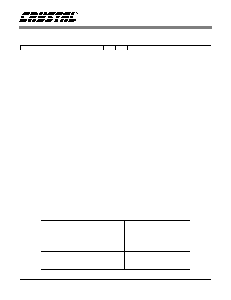
CS4205
DS489PP2
49
5.34
Internal Error Condition Control/Status Registers (Index 6Eh, Address 09h - 0Bh)
EROF
Effects Engine Right Channel Overflow
ELOF
Effects Engine Left Channel Overflow
MROF
Digital Mixer Right Channel Overflow
MLOF
Digital Mixer Left Channel Overflow
AMOR
Mic ADC Overrange
AROR
L/R ADC Right Channel Overrange
ALOR
L/R ADC Left Channel Overrange
Default
0000h
The IEC Config Register (Index 6Eh, Address 09h) enables error signaling for each potential error source. If a bit is
`clear', the corresponding source will not be monitored for errors. If a bit is `set', the corresponding source will be
monitored and is able to signal an error condition. If an error occurs, the corresponding bit in the IEC Status Register
(Index 6Eh, Address 0Bh) will be `set' and remains `set' until the error is cleared, even if the error condition is no
longer present. This behavior is equivalent to "sticky" (edge sensitive) GPIO input pins.
The IEC Wakeup Register (Index 6Eh, Address 0Ah)
provides a mask for determining if an IEC will generate a wake-
up or GPIO_INT. If a bit is `0', the corresponding error condition will not generate an interrupt. If a bit is `set', the
corresponding error condition will generate an interrupt. For details about wakeup interrupts refer to the GPIO Pin
Wakeup Mask Register (Index 52h).
The IEC Status Register (Index 6Eh, Address 0Bh)
reflects the state of all internal error conditions. If a bit is `clear',
the corresponding source has not encountered an error condition or is not being monitored for errors. If a bit is `set',
the corresponding source has encountered an error condition. The IEC bit in input slot 12 is a logic OR of all bits in
this register. An error condition is cleared by writing a `0' to the corresponding bit of this register. Before clearing an
error condition, the controller should correct the error to prevent repeated error signaling. Table 20 lists all the inter-
nal error sources and corrective measures for each source.
D15
D14
D13
D12
D11
D10
D9
D8
D7
D6
D5
D4
D3
D2
D1
D0
EROF ELOF MROF MLOF
0
AMOR AROR ALOR
0
0
0
0
0
0
0
0
IEC Bit
Error Source
Correction Method
ALOR
L/R ADC left channel overrange
GL[3:0] bits in reg 1Ch
AROR
L/R ADC right channel overrange
GR[3:0] bits in reg 1Ch
AMOR
Mic ADC overrange
GM[3:0] bits in reg 1Eh
MLOF
Digital mixer left channel overflow
GL[5:0] bits in reg 6Eh, addr 00h-05h
MROF
Digital mixer right channel overflow
GR[5:0] bits in reg 6Eh, addr 00h-05h
ELOF
Effects engine left channel overflow
GL[3:0] bits in reg 6Eh, addr 08h
EROF
Effects engine right channel overflow GR[3:0] bits in reg 6Eh, addr 08h
Table 20. Internal Error Sources and Correction Methods
CS4205
50
DS489PP2
5.35
BIOS-Driver Interface Control Registers (Index 6Eh, Address 0Ch - 0Dh)
E[15:0]
Event Configuration. The E[15:0] bits control the BIOS-Driver Interface mechanism.
Default
0000h
The BDI Config Register (Index 6Eh, Address 0Ch)
enables BIOS-Driver communication for each possible event. If
a bit is `0', the corresponding event will not be communicated. If a bit is `1', the corresponding event will be commu-
nicated by asserting the BDI bit in input slot 12. If an event occurs, the BIOS will `set' the corresponding bit in the
BDI Status Register (Index 7Ah). This bit remains `set' until it is cleared by the driver, acknowledging the event has
been handled. This behavior is equivalent to "non-sticky" (level sensitive) GPIO input pins.
The BDI Wakeup Register (Index 6Eh, Address 0Dh)
provides a mask for determining if a BDI event will generate
a wakeup or GPIO_INT. If a bit is `0', the corresponding event will not generate an interrupt. If a bit is `1', the corre-
sponding event will generate an interrupt. Refer to the GPIO Pin Wakeup Mask Register (Index 52h) for details about
wakeup interrupts.
5.36
ZV Port Control/Status Registers (Index 6Eh, Address 0Eh - 0Fh)
ZVEN
ZV Port Input Enable. The ZVEN bit enables the reception of asynchronous serial data on the
ZLRCLK, ZSDATA, and ZSCLK pins. The ZVEN bit routes the left and right channel data from
the ZV Port to the asynchronous SRC (ASRC) and on to the ZV volume control. This bit also
functions as a powerdown control for the ASRC. When this bit is `cleared', the ASRC is pow-
ered down. To use the ZV Port and the ASRC, this bit must be `set'.
LOCK
ZV Port Locked. When `set', the LOCK read-only bit indicates the ZV Port is receiving valid
data and the receiver has locked on to the data stream. If this bit is `cleared', no valid data
are received on the ZV Port and the ZV input to the digital mixer will be muted.
Ph[24:0]
Phase Increment. The Ph[24:0] bits contain the current Phase Increment used by the ASRC.
The current sample rate can be determined by Fs
in
= Fs
out
*Ph/16,777,216, where
Fs
out
is 48 kHz.
For more information on how to use these bits see Section 7, ZV Port.
Default
0000h
D15
D14
D13
D12
D11
D10
D9
D8
D7
D6
D5
D4
D3
D2
D1
D0
E15
E14
E13
E12
E11
E10
E9
E8
E7
E6
E5
E4
E3
E2
E1
E0
D15
D14
D13
D12
D11
D10
D9
D8
D7
D6
D5
D4
D3
D2
D1
D0
ZVEN LOCK
0
Ph24
Ph23
Ph22
Ph21
Ph20
Ph19
Ph18
Ph17
Ph16
Ph15
Ph14
Ph13
Ph12
Reserved
Ph11
Ph10
Ph9
Ph8
Ph7
Ph6
Ph5
Ph4
Ph3
Ph2
Ph1
Ph0
Register Address
Function
0Eh
ZV Port Control/Stat 1
0Fh
ZV Port Control/Stat 2
Table 21. ZV Port Control/Status Register Index

CS4205
DS489PP2
51
5.37
BIOS-Driver Interface Status Register (Index 7Ah)
E[15:0]
Event Status. This register, in conjunction with the BIOS-Driver Interface Control Registers
(Index 6Eh, Address 0Ch - 0Dh), controls the BIOS-Driver Interface mechanism.
Default
0000h
The BDI Status Register (Index 7Ah) reflects the state of all possible events. If a bit is `0', the corresponding event
has not occurred or has already been handled by the driver. If a bit is `1', the corresponding event has occurred and
has not been handled by the driver yet. The BDI bit in input slot 12 is a logic OR of all bits in this register ANDed
with their corresponding bit in the BDI Config Register (Index 6Eh, Address 0Ch). After handling an event, the driver
should clear it by writing a `0' to the corresponding bit of this register.
D15
D14
D13
D12
D11
D10
D9
D8
D7
D6
D5
D4
D3
D2
D1
D0
E15
E14
E13
E12
E11
E10
E9
E8
E7
E6
E5
E4
E3
E2
E1
E0

CS4205
52
DS489PP2
5.38
Vendor ID1 Register (Index 7Ch)
F[7:0]
First Character of Vendor ID. With a value of F[7:0] = 43h, these bits define the ASCII `C' char-
acter.
S[7:0]
Second Character of Vendor ID. With a value of S[7:0] = 52h, these bits define the ASCII `R'
character.
Default
4352h. This register contains read-only data.
5.39
Vendor ID2 Register (Index 7Eh)
T[7:0]
Third Character of Vendor ID. With a value of T[7:0] = 59h, these bits define the ASCII `Y'
character.
DID[2:0]
Device ID. With a value of DID[2:0] = 101, these bits specify the audio codec is a CS4205.
REV[2:0]
Revision. With a value of REV[2:0] = 001, these bits specify the audio codec revision is `A'.
Default
595xh. This register contains read-only data.
The two Vendor ID registers provide a means to determine the manufacturer of the AC '97 audio codec. The first
three bytes of the Vendor ID registers contain the ASCII code for the first three letters of Crystal (CRY). The final
byte of the Vendor ID registers is divided into a Device ID field and a Revision field. Table 22 lists the currently de-
fined Device ID's.
D15
D14
D13
D12
D11
D10
D9
D8
D7
D6
D5
D4
D3
D2
D1
D0
F7
F6
F5
F4
F3
F2
F1
F0
S7
S6
S5
S4
S3
S2
S1
S0
D15
D14
D13
D12
D11
D10
D9
D8
D7
D6
D5
D4
D3
D2
D1
D0
T7
T6
T5
T4
T3
T2
T1
T0
0
DID2
DID1
DID0
1
REV2 REV1 REV0
DID2-DID0
Part Name
000
CS4297
001
CS4297A
010
CS4294/CS4298
011
CS4299
100
CS4201
101
CS4205
110
CS4291
Table 22. Device ID with Corresponding Part Number
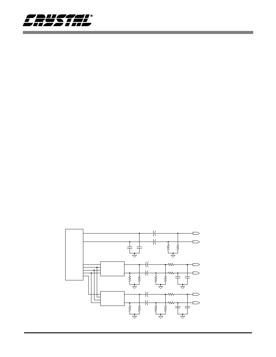
CS4205
DS489PP2
53
6. SERIAL DATA PORTS
6.1
Overview
The CS4205 implements two serial data output
ports and three serial data input ports that can be
used for digital docking or multi-channel expan-
sion. Each serial port consists of 4 signals: MCLK,
SCLK, LRCLK, and SDATA. The existing 256 Fs
BIT_CLK will be used as MCLK. The clock pins
are shared between all the serial ports with only the
SDATA pins being separate; SDOUT for the first
output port, SDO2 for the second output port, and
SDI[3:1] for the three input ports. Serial data is re-
ceived and transmitted on these ports every
AC-link frame.
The serial data port is controlled by the SDEN,
SDSC, SDI[3:1], and SDO2 bits in the Serial Port
Control Register (Index 6Ah). All the serial data
port pins are multiplexed with other functions and
cannot be used unless the other function is disabled
or powered down; see Section 9, Exclusive Func-
tions. Some audio DACs can run in an internal
SCLK mode where SCLK is internally derived
from MCLK and LRCLK. In this case, SCLK gen-
eration in the CS4205 is optional.
A feature has been designed into the CS4205 that
allows the phase of the internal DACs to be re-
versed. This DAC phase reversal is controlled by
the DPC bit in the Misc. Crystal Control Register
(Index 60h). This feature is necessary since the
phase response for external DACs is unknown and
the phase response of the internal DACs can vary
depending on the path determined by the DDM bit
in the AC Mode Control Register (Index 5Eh). This
feature guarantees that all DACs in a system have
the same phase response, maintaining the accuracy
of spatial cues.
In the CS4205, the volume of the serial port data is
controlled with the Serial Data Port Volume Con-
trol Registers (Index 6Eh, Address 06h - 07h).
However, there is no SRC available on this data, so
it is the responsibility of the controller or host soft-
ware to provide this functionality if desired.
6.2
Multi-Channel Expansion
For multi-channel expansion, the two serial data
output ports are used to send AC-link data to one or
two external stereo DACs to support up to a total of
six channels. The first serial port takes the digital
audio data from the SDOUT slots. The second seri-
al port takes the digital audio data from the SDO2
slots. See Table 14 on page 42 for the actual slots
used depending on configuration. Figure 15 shows
a six channel application using the CS4205.
8
5
4
3
2
1
4
3
2
1
8
5
AOUTL
AOUTR
SDATA
DEM#/SCLK
LRCK
MCLK
GPIO1/SDOUT
SPDO/SDO2
44
48
47
43
EAPD/SCLK
GPIO0/LRCLK
LINE_OUT_L
LINE_OUT_R
BIT_CLK
6
36
35
CS4334
AOUTL
AOUTR
SDATA
DEM#/SCLK
LRCK
MCLK
CS4334
270K
270K
10uF
ELEC
10uF
ELEC
47K
47K
560
560
2700pF 2700pF
Left Surround
Right Surround
270K
270K
10uF
ELEC
10uF
ELEC
47K
47K
560
560
2700pF 2700pF
Center
LFE
AGND
AGND
AGND
AGND
Left Front
Right Front
AGND
AGND
10uF
ELEC
10uF
ELEC
1000pF
AGND
220K
220K
AGND
1000pF
+
+
+
+
+
+
Figure 15. Serial Data Port: Six Channel Circuit

CS4205
54
DS489PP2
6.3
Digital Docking
The CS4205 features three serial data input ports
used to receive data from three stereo ADCs inside
a docking station. One serial data output port is
used to transmit data to a stereo DAC inside the
docking station. To fully utilize digital docking, the
CS4205 should be configured for digital centric
mode; see Section 3.2, Digital Centric Mode. This
will allow the docking sources to be mixed with the
analog sources from the notebook. The resulting
mix is available for listening on both the notebook
and the docking station and for capturing on the
host. Figure 16 shows a block diagram for digital
docking applications of the CS4205.
Note the BIT_CLK output should be buffered be-
fore sending it as MCLK to the docking station
converters. The capacitance loading of the docking
station connector, the relatively long trace, and the
multiple loads on this signal may exceed the load-
ing restrictions on BIT_CLK. Buffering of SCLK
and LRCLK should also be considered.
6.4
Serial Data Formats
In order to support a wide variety of serial audio
DACs and ADCs, the CS4205 can transmit and re-
ceive serial data in four different formats. The de-
sired format is selected through the SDF[1:0] bits
in the Serial Port Control Register (Index 6Ah). All
serial ports use the same serial data format when
enabled. In all cases, LRCLK will be synchronous
with Fs, and SCLK will be 64 Fs (BIT_CLK/4).
Serial data is transitioned by the CS4205 on the
falling edge of SCLK and latched by the DACs on
the next rising edge. Serial data is shifted out MSB
first in all supported formats, but LRCLK polarity
as well as data justification, alignment, and resolu-
tion vary. Table 23 shows the principal characteris-
tics of each serial format.
Stereo DAC
Stereo ADC
SCLK
CS4205
Line Out L
Line Out R
Mic In L
Mic In R
LRCLK
SDOUT
SDI1
SDI2
SDI3
Stereo ADC
Line In L
Line In R
Stereo ADC
CD In L
CD In R
BIT
_
C
L
K
SD
AT
A_
IN
SD
AT
A_
OU
T
SYN
C
R
ESET
#
MCLK
DC '97
Controller
Notebook Side
Docking Station Side
Figure 16. Digital Docking Connection Diagram
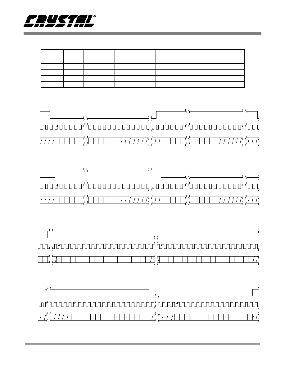
CS4205
DS489PP2
55
SDF[1:0]
LRCLK
Polarity
Data
Justification
Data Alignment
(MSB vs. LRCLK)
Data
Resolution
Timing
Diagram
Recommended
DAC/ADC
0 0
negative
left justified
1 SCLK delayed
20-bit
Figure 17
CS4334/CS5331A
0 1
positive
left justified
not delayed
20-bit
Figure 18
CS4335/CS5330A
1 0
positive
right justified
not delayed
20-bit
Figure 19
CS4337/none
1 1
positive
right justified
not delayed
16-bit
Figure 20
CS4338/none
Table 23. Serial Data Formats and Compatible DACs/ADC's for the CS4205
LRCK
SCLK
Left Channel
Right Channel
SDATA
+3 +2 +1 LSB
+5 +4
MSB-1 -2 -3 -4 -5
+3 +2 +1 LSB
+5 +4
MSB-1 -2 -3 -4
Figure 17. Serial Data Format 0 (I
2
S)
LRCK
SCLK
Left Channel
Right Channel
SDATA
+3 +2 +1 LSB
+5 +4
MSB-1 -2 -3 -4 -5
+3 +2 +1 LSB
+5 +4
MSB-1 -2 -3 -4
Figure 18. Serial Data Format 1 (Left Justified)
LRCK
SCLK
Left Channel
Right Channel
SDATA
6 5 4 3 2 1 0
9 8 7
15 14 13 12 11 10
1 0
6 5 4 3 2 1 0
9 8 7
15 14 13 12 11 10
17 16
17 16
19 18
19 18
Figure 19. Serial Data Format 2 (Right Justified, 20-bit data)
LRCK
SCLK
Left Channel
Right Channel
SDATA
6
5
4
3
2
1 0
9
8 7
15 14 13 12 11 10
6
5
4
3 2
1
0
9
8
7
15 14 13 12 11 10
Figure 20. Serial Data Format 3 (Right Justified, 16-bit data)
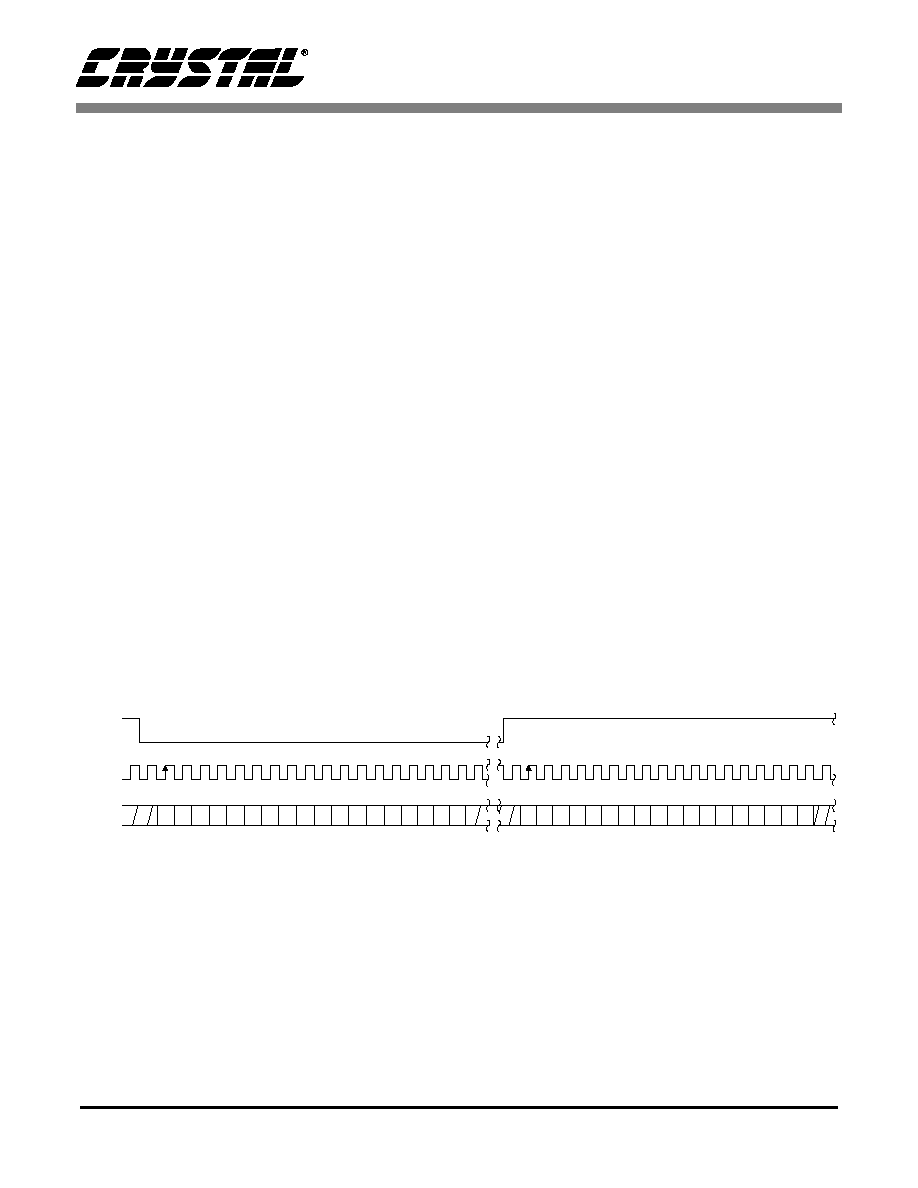
CS4205
56
DS489PP2
7. ZV PORT
The CS4205 implements an asynchronous serial
data input port that conforms to the Zoomed Video
Port (ZV Port) specification. ZV Port data is asyn-
chronous I
2
S data in PCM format with 16 bits of
resolution. The ZV Port interface consists of four
signals: MCLK, SCLK, LRCLK, and SDATA.
However, the CS4205 does not require a connec-
tion to the asynchronous MCLK. The other three
signals are respectively received on ZSCLK, ZLR-
CLK, and ZSDATA. Although the ZV Port speci-
fication calls for SCLK running at 32 Fs, the
CS4205 supports any SCLK from 32 Fs up to
128 Fs. In all cases, only the first 16 bits of each
channel will be recovered from the incoming serial
data stream. Figure 21 shows the ZV Port format.
The ZV Port is controlled by the ZVEN, LOCK,
and Ph[24:0] bits in the ZV Port Control/Status
Registers (Index 6Eh, Address 0Eh - 0Fh).
Since the data received on the ZV Port is asynchro-
nous and at varying sample rates, it must be sample
rate converted before being sent to the digital mix-
er. The asynchronous SRC is similar in function to
the synchronous DAC SRC, but differs in the way
samples are received and how the sample rate is de-
termined. While the synchronous SRC is being pro-
grammed to the desired sample rate by the host and
requests samples from the host at the programmed
rate, the asynchronous SRC receives data from a
push source at an unknown rate. Therefore, the
asynchronous SRC must determine the rate of in-
coming data and calculate the necessary parame-
ters. The current sample rate can be determined
from the Ph[24:0] bits in the ZV Port Control/Sta-
tus Registers (Index 6Eh, Address 0Eh - 0Fh) by
Fs
in
= Fs
out
*Ph/16,777,216, where Fs
out
is
48 kHz. Once the rate estimator has settled, the
LOCK bit will be asserted. If the incoming clock
rate changes, LOCK will be de-asserted until the
rate estimator has settled again. Settling may take
up to 400 ms. As long as the receiver is unlocked,
the ZV input to the digital mixer will be muted, re-
gardless of the state of the ZV mute bit in the Dig-
ital Mixer Input Volume Register (Index 6E,
Address 00h - 05h).
ZLRCK
ZSCLK
Left Channel
Right Channel
ZSDATA
6
5
4
3
2
1 0
9
8
7
15 14 13 12 11 10
6 5
4 3
2 1
0
9 8 7
15 14 13 12 11 10
Figure 21. ZV Port Format (I
2
S, 16-bit data)
CS4205
DS489PP2
57
8. SONY/PHILIPS DIGITAL
INTERFACE (S/PDIF)
The S/PDIF digital output is used to interface the
CS4205 to consumer audio equipment external to
the PC. This output provides an interface for stor-
ing digital audio data or playing digital audio data
to digital speakers. Figure 22 illustrates the circuits
necessary for implementing the IEC-958 optical or
consumer interface. For further information on
S/PDIF operation see application note AN22: Over-
view of Digital Audio Interface Data Structures [3].
For further information on S/PDIF recommended
transformers see application note AN134: AES and
S/PDIF Recommended Transformers [4].
1
2
3
4
5
6
0.1
µF
R
2
R
1
J1
DGND
DVdd
R
1
R
2
SPDO/SDO2
S/PDIF_OUT
TOTX-173
SPDO/SDO2
+5V_PCI
DGND
8.2 k
DGND
DGND
3.3V
247.5
107.6
5V
375
93.75
T
1
Figure 22. S/PDIF Output

CS4205
58
DS489PP2
9. EXCLUSIVE FUNCTIONS
Some of the digital pins on the CS4205 have mul-
tiplexed functionality. These functions are mutual-
ly exclusive and cannot be requested at the same
time. The following pairs of functions are mutually
exclusive:
∑
GPIO and Serial Data Port (GPIO0 pin is
shared with LRCLK pin, GPIO1 pin is shared
with SDOUT pin, and GPIO[4:2] pins are
shared with SDI[3:1] pins)
∑
EAPD and Serial Data Port Serial Clock
(EAPD pin is shared with SCLK pin)
∑
S/PDIF and Second Serial Data Port (SPDO pin
is shared with SDO2 pin)
Use of the GPIO0/LRCLK, GPIO1/SDOUT, and
GPIO[4:2]/SDI[3:1] pins for serial data port has
priority over their GPIO functionality. There is no
priority assigned to the other two exclusive func-
tions. A function currently in use must be disabled
or powered down before the corresponding exclu-
sive function can be enabled. The following control
bits for these functions will behave differently than
normal bits: the EAPD bit in the Powerdown Con-
trol/Status Register (Index 26h), the GC[4:0] bits in
the GPIO Pin Config Register (Index 4Ch), the
SPEN bit in the S/PDIF Control Register
(Index 68h), and the SDI[3:1], SDO2, and SDSC
bits in the Serial Port Control Register
(Index 6Ah). These bits can become read-only bits
if they control a feature that is currently unavailable
because the corresponding exclusive feature is al-
ready in use, or the corresponding master control
for this feature is not set.

CS4205
DS489PP2
59
10. POWER MANAGEMENT
10.1
AC '97 Reset Modes
The CS4205 supports four reset methods, as de-
fined in the AC '97 Specification: Cold Reset,
Warm Reset, New Warm Reset, and Register Reset.
A Cold Reset results in all AC '97 logic (registers
included) initialized to its default state. A Warm
Reset or New Warm Reset leaves the contents of
the AC '97 register set unaltered. A Register Reset
initializes only the AC '97 registers to their default
states.
10.1.1
Cold Reset
A Cold Reset is achieved by asserting RESET# for
a minimum of 1 µs after the power supply rails
have stabilized. This is done in accordance with the
minimum timing specifications in the AC '97 Seri-
al Port Timing section on page 10. Once de-assert-
ed, all of the CS4205 registers will be reset to their
default power-on states and the BIT_CLK and
SDATA_IN signals will be reactivated.
10.1.2
Warm Reset
A Warm Reset allows the AC-link to be reactivated
without losing information in the CS4205 registers.
A Warm Reset is required to resume from a D3
hot
state where the AC-link had been halted yet full
power had been maintained. A primary codec
Warm Reset is initiated when the SYNC signal is
driven high for at least 1 µs and then driven low in
the absence of the BIT_CLK clock signal. The
BIT_CLK clock will not restart until at least 2 nor-
mal BIT_CLK clock periods (162.8 ns) after the
SYNC signal is de-asserted. A Warm Reset of the
secondary codec is recognized when the primary
codec on the AC-link resumes BIT_CLK genera-
tion. The CS4205 will wait for BIT_CLK to be sta-
ble to restore SDATA_IN activity, S/PDIF and/or
serial data port transmission on the following
frame.
10.1.3
New Warm Reset
The New Warm Reset also allows the AC-link to
be reactivated without losing information in the
registers. A New Warm Reset is required to resume
from a D3
cold
state where AC-link power has been
removed. New Warm Reset is recognized by the
low-high transition of RESET# after the AC-link
has been programmed into PR4 powerdown. The
New Warm Reset functionality can be disabled by
setting the CRST bit in the Misc. Crystal Control
Register (Index 60h).
10.1.4
Register Reset
The last reset mode provides a Register Reset to the
CS4205. This is available only when the CS4205
AC-link is active and the Codec Ready bit is `set'.
The audio (including extended audio) control reg-
isters (Index 00h - 3Ah) and the vendor specific
registers (Index 5Ah - 7Ah) are reset to their default
states by a write of any value to the Reset Register
(Index 00h). The modem (including GPIO) regis-
ters (Index 3Ch - 56h) are reset to their default
states by a write of any value to the Extended Mo-
dem ID Register (Index 3Ch).
CS4205
60
DS489PP2
10.2
Powerdown Controls
The
Powerdown Control/Status Register
(Index 26h) controls the power management func-
tions. The PR[5:0] bits in this register control the
internal powerdown states of the CS4205. Power-
down control is available for individual subsections
of the CS4205 by asserting any PRx bit or any com-
bination of PRx bits. All powerdown states except
PR4 and PR5 can be resumed by clearing the cor-
responding PRx bit. Table 24 shows the mapping
of the power control bits to the functions they man-
age.
When PR0 is `set', the L/R ADCs and the Input
Mux are shut down and the ADC bit in the Power-
down Control/Status Register (Index 26h) is
`cleared' indicating the ADCs are no longer in a
ready state. The same is true for PR1 and the
DACs, PR2 and the analog mixer, and PR3 and the
voltage reference (Vrefout). When one of these bits
is `cleared', the corresponding subsystem will be-
gin a power-on process, and the associated status
bit will be `set' when the hardware is ready.
In a primary codec the PR4 bit powers down the
AC-link, but all other analog and digital sub-
systems continue to function. The required resume
sequence from a PR4 state is either a Warm Reset
or a New Warm Reset, depending on whether a
D3
hot
or D3
cold
state has been entered.
The PR5 bit disables all internal clocks and powers
down the DACs and the ADCs, but maintains oper-
ation of the BIT_CLK and the analog mixer. A
Cold Reset is the only way to restore operation to
the CS4205 after asserting PR5. To achieve a com-
plete digital powerdown, PR4 and PR5 must be as-
serted within a single AC output frame. This will
also drive BIT_CLK `low'.
The CS4205 does not automatically mute any input
or output when the powerdown bits are `set'. The
software driver controlling the AC '97 device must
manage muting the input and output analog signals
before putting the part into any power management
state. The definition of each PRx bit may affect a
single subsection or a combination of subsections
within the CS4205. Table 25 contains the matrix of
subsections affected by the respective PRx func-
tion. Table 26 shows the different operating power
consumptions levels for different powerdown func-
tions.
PR Bit
Function
PR0
L/R ADCs and Input Mux Powerdown
PR1
Front DACs Powerdown
PR2
Analog Mixer Powerdown (Vref on)
PR3
Analog Mixer Powerdown (Vref off)
PR4
AC-link Powerdown (BIT_CLK off)*
PR5
Internal Clock Disable
* Applies only to primary codec
Table 24. Powerdown PR Bit Functions
CS4205
DS489PP2
61
PR Bit
ADCs
DACs
Mixer
Analog
Reference
AC
Link
Internal
Clock Off
Mic ADC
PR0
∑
PR1
∑
PR2
∑
∑
∑
∑
PR3
∑
∑
∑
∑
∑
PR4
∑
PR5
∑
∑
∑
∑
PRL
∑
Table 25. Powerdown PR Function Matrix for the CS4205
Power State
I
DVdd1
(mA)
[DVdd=3.3 V]
I
DVdd1
(mA)
[DVdd=5 V]
I
AVdd1
(mA)
Full Power + SRC's
TBD
TBD
TBD
Full Power + S/PDIF
1
1
Assuming standard resistive load for transformer coupled coaxial S/PDIF output
(Rload = 292 Ohm, DVdd = 3.3 V) (Rload = 415 Ohm, DVdd = 5 V). General: I
DVdd
S/PDIF
= I
DVdd
+ DVdd/Rload/2
TBD
TBD
TBD
Full Power
TBD
TBD
TBD
ADCs off (PR0)
TBD
TBD
TBD
DACs off (PR1)
TBD
TBD
TBD
Audio off (PR2)
TBD
TBD
TBD
Vref off (PR3)
TBD
TBD
TBD
AC-Link off (PR4)
TBD
TBD
TBD
Internal Clocks off (PR5)
TBD
TBD
TBD
Digital off (PR4+PR5)
TBD
TBD
TBD
PR3+PR4+PR5
TBD
TBD
TBD
RESET
TBD
TBD
TBD
Table 26. Power Consumption by Powerdown Mode for the CS4205

CS4205
62
DS489PP2
11. CLOCKING
The CS4205 may be operated as a primary or sec-
ondary codec. As a primary codec, the system
clock for the AC-link may be generated from an ex-
ternal 24.576 MHz clock source, a 24.576 MHz
crystal, or use the internal Phase Locked Loop
(PLL). The PLL allows the CS4205 to accept exter-
nal clock frequencies other than 24.576 MHz. The
CS4205 uses the presence or absence of a valid
clock on the XTL_IN pin in conjunction with the
ID[1:0]# pins to determine the clocking configura-
tion.
11.1
PLL Operation (External Clock)
The PLL mode is activated if a valid clock is
present on XTL_IN during the rising edge of
RESET#. Once PLL mode is entered, the
XTL_OUT pin is redefined as the PLL loop filter,
as shown in Figure 23. The ID[1:0]# inputs deter-
mine the configuration of the internal divider ratios
required to generate the 12.288 MHz BIT_CLK
output; see Table 27 on page 63 for additional de-
tails. In PLL mode, the CS4205 is configured as a
primary codec independent of the state of the
ID[1:0]# pins. If 24.576 MHz is chosen as the ex-
ternal clock input (ID[1:0]# inputs both pulled high
or left floating), the PLL is disabled and the clock
is used directly. The loop filter is not required and
XTL_OUT is left unconnected. For all other clock
input choices, the loop filter is required. The
ID[1:0] bits of the Extended Audio ID Register
(Index 28h) and the Extended Modem ID Register
(Index 3Ch) will always report 0 in PLL mode.
11.2
24.576 MHz Crystal Operation
If a valid clock is not present on XTL_IN during
the rising edge of RESET#, the device disables the
PLL input and latches the state of the ID[1:0]# in-
puts. If the ID[1:0]# inputs are both pulled high or
left floating, the device is configured as a primary
codec. An external 24.576 MHz crystal is used as
the system clock as shown in Figure 24.
11.3
Secondary Codec Operation
If a valid clock is not present on XTL_IN and either
ID[1:0]# input is pulled low during the rising edge
of RESET#, the device is determined to be a sec-
ondary codec. The BIT_CLK pin is configured as
an input and the CS4205 is driven from the
12.288 MHz BIT_CLK of the primary codec. The
ID[1:0] bits of the Extended Audio ID Register
(Index 28h) and the Extended Modem ID Register
(Index 3Ch) will report the state of the ID[1:0]#
inputs.
Figure 23. PLL External Loop Filter
XTL_OUT
XTL_IN
2.2 k
0.022 uF
220 pF
Clock Source
DGND
22 pF
22 pF
24.576 MHz
DGND
XTL_OUT
XTL_IN
Figure 24. External Crystal
CS4205
DS489PP2
63
External
Clock on
XTL_IN
ID1# ID0#
AC-Link
Timing
Mode
Codec
ID
Clock
Source
Clock
Rate
(MHz)
PLL
Active
Application Notes
Yes
1
1
Primary
0
External
24.576
No
clock generator driving XTL_IN
Yes
1
0
Primary
0
External
14.31818
Yes
external clock source driving XTL_IN
loop filter connected to XTL_OUT
Yes
0
1
Primary
0
External
27.000
Yes
Yes
0
0
Primary
0
External
48.000
Yes
No
1
1
Primary
0
XTAL
24.576
No
crystal connected to XTL_IN, XTL_OUT
No
1
0
Secondary
1
BIT_CLK
12.288
No
BIT_CLK from primary codec driving
BIT_CLK on all secondary codecs
No
0
1
Secondary
2
BIT_CLK
12.288
No
No
0
0
Secondary
3
BIT_CLK
12.288
No
Table 27. Clocking Configurations for the CS4205
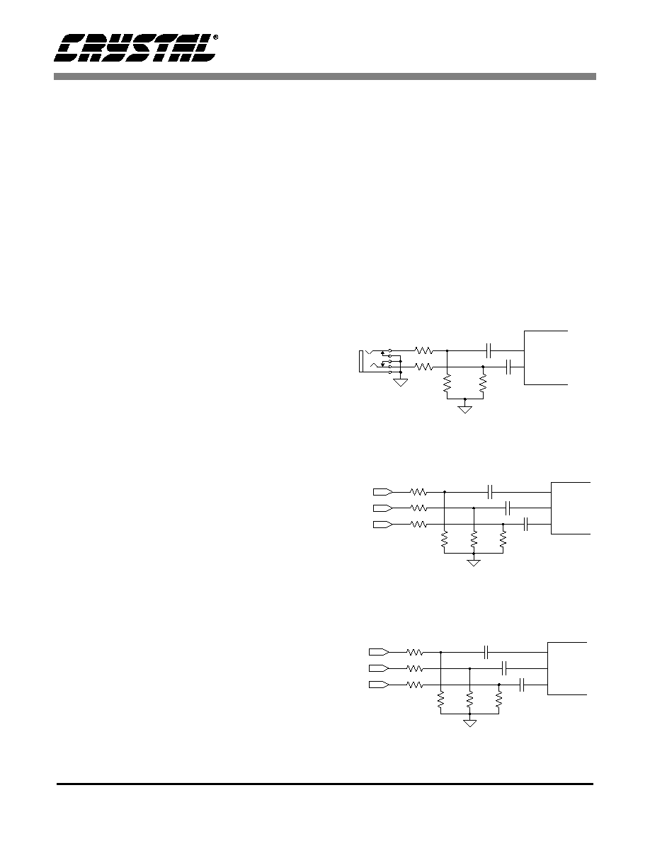
CS4205
64
DS489PP2
12. ANALOG HARDWARE
DESCRIPTION
The analog input section consists of four stereo
line-level inputs (LINE_L/R, CD_L/GND/R,
VIDEO_L/R, and AUX_L/R), two selectable
mono microphone inputs (MIC1 and MIC2), and
two mono inputs (PC_BEEP and PHONE). The an-
alog output section consists of a mono output
(MONO_OUT) and a stereo line-level output
(LINE_OUT_L/R). This section describes the ana-
log hardware needed to interface with these pins.
The designs presented in this section are compliant
with Chapter 17 of Microsoft's
PC 99 System De-
sign Guide [7] (referred to as PC 99) and Chapter
11 of Microsoft's
PC 2001 System Design Guide
[8] (referred to as PC 2001). For information on
EMI reduction techniques refer to the application
note AN165: CS4297A/CS4299 EMI Reduction
Techniques [5].
12.1
Analog Inputs
All analog inputs to the CS4205, including
CD_GND, should be capacitively coupled to the
input pins. Unused analog inputs should be tied to-
gether and connected through a capacitor to analog
ground or tied to the Vrefout pin directly. The max-
imum allowed voltage for analog inputs, except the
microphone input, is 1 V
RMS
. The maximum al-
lowed voltage for the microphone input depends on
the selected boost setting.
12.1.1
Line Inputs
Figure 25 shows circuitry for a line-level stereo in-
put. Replicate this circuit for the Line, Video and
Aux inputs. This design attenuates the input by
6 dB, bringing the signal from the PC 99 specified
2 V
RMS
, to the CS4205 maximum allowed 1 V
RMS
.
12.1.2
CD Input
The CD line-level input has an extra pin,
CD_GND, providing a pseudo-differential input
for both CD_L and CD_R. This pin takes the
common-mode noise out of the CD inputs when
connected to the CD analog source ground. Follow-
ing the reference designs in Figure 26 and
Figure 27 provides extra attenuation of common
mode noise coming from the CD-ROM drive,
thereby producing a higher quality signal. One per-
cent resistors are recommended since closely
matched resistor values provide better com-
mon-mode attenuation of unwanted signals. The
circuit shown in Figure 26 can be used to attenuate
a 2 V
RMS
CD input signal by 6 dB. The circuit
shown in Figure 27 can be used for a 1 V
RMS
CD in-
put signal.
LINE_IN_R
LINE_IN_L
6.8 k
1.0
µ F
1.0
µ F
AGND
AGND
6.8 k
6.8 k
6.8 k
Figure 25. Line Input (Replicate for Video and AUX)
(All resistors 1%)
6.8 k
CD_L
CD_COM
CD_R
1.0
µF
CD_L
CD_R
CD_GND
6.8 k
1.0
µF
3.4 k
6.8 k
2.2
µF
3.4 k
6.8 k
AGND
Figure 26. Differential 2 V
RMS
CD Input
100
CD_L
CD_COM
CD_R
1.0
µF
CD_L
CD_R
CD_GND
100
1.0
µF
100
47 k
2.2
µF
47 k
47 k
AGND
Figure 27. Differential 1 V
RMS
CD Input

CS4205
DS489PP2
65
12.1.3
Microphone Inputs
Figure 28 illustrates an input circuit suitable for dy-
namic and electret microphones. Electret, also
known as phantom-powered, microphones use the
right channel (ring) of the jack for power. The de-
sign also supports the recommended advanced fre-
quency response for voice recognition as specified
in PC 99 and PC 2001. The microphone input of the
CS4205 has an integrated pre-amplifier. Using
combinations of the 10dB bit in the Misc. Crystal
Control Register (Index 60) and the 20dB bit in the
Mic Volume Register (Index 0Eh) the pre-amplifier
gain can be set to 0 dB, 10 dB, 20 dB, or 30 dB.
12.1.4
PC Beep Input
The PC_BEEP input is useful for mixing the output
of the "beeper" (timer chip), provided in most PCs,
with the other audio signals. When the CS4205 is
held in reset, PC_BEEP is passed directly to the
line output. This allows the system sounds or
"beeps" to be available before the AC '97 interface
has been activated. Figure 29 illustrates a typical
input circuit for the PC_BEEP input. If PC_BEEP
is driven from a CMOS gate, the 4.7 k
resistor
should be tied to analog ground instead of +5VA.
Although this input is described for a low-quality
"beeper", it is of the same high-quality as all other
analog inputs and may be used for other purposes.
12.1.5
Phone Input
One application of the PHONE input is to interface
to the output of a modem analog front end (AFE)
device so that modem dialing signals and protocol
negotiations may be monitored through the audio
system. Figure 30 shows a design for a modem
connection where the output is fed from the
CS4205 MONO_OUT pin through a divider. The
divider ratio shown does not attenuate the signal,
providing an output voltage of 1 V
RMS
. If a lower
output voltage is desired, the resistors can be re-
placed with appropriate values, as long as the total
load on the output is kept greater than 10 k
. The
PHONE input is divided by 6 dB to accommodate
a line-level source of 2 V
RMS
.
12.2
Analog Outputs
The analog output section provides a stereo and a
mono output. The MONO_OUT, LINE_OUT_L,
and LINE_OUT_R pins require 680 pF to 1000 pF
NPO dielectric capacitors between the correspond-
ing pin and analog ground. Each analog output is
DC-biased up to the Vrefout voltage signal refer-
ence, nominally 2.4 V. This requires the outputs be
AC-coupled to external circuitry (AC loads must
be greater than 10 k
for the line output).
0.1
µF
X7R
100
0.1
µ F
X7R
MIC1/MIC2
10
µF
ELEC
AGND
+5VA
2.2 k
1.5 k
AGND
AGND
+
Figure 28. Microphone Input
4.7 k
PC_BEEP
+5VA (Low Noise) or
AGND if CMOS Source
PC-BEEP-BUS
47 k
2.7 nF
X7R
0.1
µF
X7R
AGND
Figure 29. PC_BEEP Input
PHONE
MONO_OUT
PHONE
MONO_OUT
6.8 k
1.0
µF
0
6.8 k
1.0
µF
47 k
AGND
AGND
1000 pF
Figure 30. Modem Connection

CS4205
66
DS489PP2
12.2.1
Stereo Output
See Figure 31 for a stereo line-level output refer-
ence design.
12.2.2
Mono Output
The mono output, MONO_OUT, can be either a
sum of the left and right output channels, attenuat-
ed by 6 dB to prevent clipping at full scale, or the
selected Mic signal. The mono out channel can
drive the PC internal mono speaker using an appro-
priate buffer circuit
12.3
Miscellaneous Analog Signals
The AFLT1, AFLT2, and AFLT3 pins must have a
1000 pF NPO capacitor to analog ground. These
capacitors provide a single-pole low-pass filter at
the inputs to the ADCs. This makes low-pass filters
at each analog input pin unnecessary.
The REFFLT pin must have a short, wide trace to a
2.2
µF and a 0.1 µF capacitor connected to analog
ground (see Figure 33 in Section 13, Grounding
and Layout, for an example). The 2.2
µF capacitor
must not be replaced by any other value and must
be ceramic with low leakage current. Electrolytic
capacitors should not be used. No other connection
should be made, as any coupling onto this pin will
degrade the analog performance of the CS4205.
Likewise, digital signals should be kept away from
REFFLT for similar reasons.
12.4
Power Supplies
The power supplies providing analog power should
be as clean as possible to minimize coupling into
the analog section which could degrade analog per-
formance. The +5 VA supply should be generated
from a voltage regulator (7805 type) connected to a
+12 VD supply. This helps isolate the analog cir-
cuitry from noise typically found on +5 VD sup-
plies which power many digital circuits in a PC
environment. A typical voltage regulator circuit for
analog power using an MC78M05CDT is shown in
Figure 32. The AVdd1/AVss1 analog pow-
er/ground pin pair on the CS4205 supplies power to
all the analog circuitry and should be connected to
+5 VA/AGND. The AVdd2 and AVss2 pins are not
used on the CS4205 and may be left floating or tied
to +5 VA/AGND for backwards compatibility.
The DVdd2/DVss2 digital power/ground pin pair
on the CS4205 should be connected to the same
digital supply as the controller AC-link interface.
Since the digital interface on the CS4205 may op-
erate at either +3.3 VD or +5 VD, proper connec-
tion of these pins will depend on the digital power
supply of the controller. The DVdd1/DVss1 pair
supplies power to the clocking circuitry and needs
to be connected to the +5 VA/AGND power supply
when the CS4205 is in PLL clocking mode. In
XTAL or OSC clocking modes these pins may be
connected to either +5 VA/AGND or use the same
power supply used for DVdd2/DVss2
12.5
Reference Design
See Section 16 for a CS4205 reference design.
LINE_OUT_R
LINE_OUT_L
10
µF
ELEC
10
µF
ELEC
220 k
220 k
AGND
1000 pF
1000 pF
AGND
+
+
Line Out
Figure 31. Stereo Output
Figure 32. +5V Analog Voltage Regulator
3
2
1
AGND
GND
IN
OUT
MC78M05CDT
+12VD
10
µF
ELEC
+
0.1
µF
Y5V
10
µF
ELEC
+
0.1
µF
Y5V
DGND
+5VA

CS4205
DS489PP2
67
13.
GROUNDING AND LAYOUT
Figure 33 on page 68 shows the conceptual layout
for the CS4205 in XTAL or OSC clocking modes.
The decoupling capacitors should be located phys-
ically as close to the pins as possible. Also, note the
connection of the REFFLT decoupling capacitors
to the ground return trace connected directly to the
ground return pin, AVss1.
It is strongly recommended that separate analog
and digital ground planes be used. Separate ground
planes keep digital noise and return currents from
modulating the CS4205 ground potential and de-
grading performance. The digital ground pins
should be connected to the digital ground plane and
kept separate from the analog ground connections
of the CS4205 and any other external analog cir-
cuitry. All analog components and traces should be
located over the analog ground plane and all digital
components and traces should be located over the
digital ground plane.
The common connection point between the two
ground planes (required to maintain a common
ground voltage potential) should be located under
the CS4205. The AC-link digital interface connec-
tion traces should be routed such that the digital
ground plane lies underneath these signals (on the
internal ground layer). This applies along the entire
length of these traces from the AC '97 controller to
the CS4205.
Refer to the Application Note AN18: Layout and
Design Rules for Data Converters and Other
Mixed Signal Devices [2] for more information on
layout and design rules.

CS4205
68
DS489PP2
Analog
Ground
Pin 1
0.1 µF
1000 pF
NPO
2.2 µF
0.1 µF
Y5V
0.1 µF
Y5V
Y5V
0.1 µF
Y5V
AVdd2
AVss2
AFLT2
REFFLT
AVss1
AVdd1
DVdd2
AFLT1
AFLT3
Digital
Ground
DVss2
DVss1
DVdd1
Vrefout
to via
Via to +5VA
Via to +5VA
Via to Analog
Ground
Via to Analog
Ground
Via to Digital Ground
Via to +5VD or +3.3VD
Via to +5VD or +3.3VD
Figure 33. Conceptual Layout for the CS4205 when in XTAL or OSC Clocking Modes
CS4205
DS489PP2
69
14. PIN DESCRIPTIONS
CS4205
48
47
46
45
44
43
42
41
40
39
38
37
M
O
NO
_
O
UT
AVdd2
GPIO2/SD
I1
GPIO3/SD
I2
GPIO4/SD
I3
A
V
ss2
G
P
I
O
0
/
L
RCL
K
GP
IO1/S
D
OU
T
ID
0#
ID
1#
EAPD/SCLK
SPDO
/
SDO
2
1
2
3
4
5
6
7
8
9
10
11
12
DVdd1
XTL_IN
XTL_OUT
DVss1
SDATA_OUT
BIT_CLK
DVss2
SDATA_IN
DVdd2
SYNC
RESET#
PC_BEEP
13
14
15
16
17
18
19
20
21
22
23
24
LIN
E
_IN
_
R
LIN
E
_IN
_
L
MIC
2
MIC
1
CD_
R
CD_
G
N
D
CD_
L
VIDEO
_
R
VIDEO
_
L
AUX_R
AUX_L
PHO
N
E
36
35
34
33
32
31
30
29
28
27
26
25
LINE_OUT_R
LINE_OUT_L
ZSCLK
ZSDATA
ZLRCLK
AFLT3
AFLT2
AFLT1
Vrefout
REFFLT
AVss1
AVdd1
Figure 34. Pin Locations for the CS4205

CS4205
70
DS489PP2
Audio I/O Pins
PC_BEEP - Analog Mono Source, Input, Pin 12
The PC_BEEP input is intended to allow the PC system POST (Power On Self-Test) tones to pass
through to the audio subsystem. The PC_BEEP input has two connections: the first connection is to the
analog output mixer, the second connection is directly to the LINE_OUT stereo outputs. While the
RESET# pin is actively being asserted to the CS4205, the PC_BEEP bypass path to the LINE_OUT
outputs is enabled. While the CS4205 is in normal operation mode with RESET# de-asserted,
PC_BEEP is a monophonic source to the analog output mixer. The maximum allowable input is 1 V
RMS
(sinusoidal). This input is internally biased at the Vrefout voltage reference and requires AC-coupling to
external circuitry. If this input is not used, it should be connected to the Vrefout pin or AC-coupled to
analog ground.
PHONE - Analog Mono Source, Input, Pin 13
This analog input is a monophonic source to the output mixer. It is intended to be used as a modem
subsystem input to the audio subsystem. The maximum allowable input is 1 V
RMS
(sinusoidal). This
input is internally biased at the Vrefout voltage reference and requires AC-coupling to external circuitry.
If this input is not used, it should be connected to the Vrefout pin or AC-coupled to analog ground.
MIC1 - Analog Mono Source, Input, Pin 21
This analog input is a monophonic source to the analog output mixer. It is intended to be used as a
desktop microphone connection to the audio subsystem. The CS4205 internal mixer's microphone input
is MUX selectable with either MIC1 or MIC2 as the input. The maximum allowable input is 1 V
RMS
(sinusoidal). This input is internally biased at the Vrefout voltage reference and requires AC-coupling to
external circuitry. If this input is not used, it should be connected to the Vrefout pin or AC-coupled to
analog ground.
MIC2 - Analog Mono Source, Input, Pin 22
This analog input is a monophonic source to the analog output mixer. It is intended to be used as an
alternate microphone connection to the audio subsystem. The CS4205 internal mixer's microphone input
is MUX selectable with either MIC1 or MIC2 as the input. The maximum allowable input is 1 V
RMS
(sinusoidal). This input is internally biased at the Vrefout voltage reference and requires AC-coupling to
external circuitry. If this input is not used, it should be connected to the Vrefout pin or AC-coupled to
analog ground.
LINE_IN_L, LINE_IN_R - Analog Line Source, Inputs, Pins 23 and 24
These inputs form a stereo input pair to the CS4205. The maximum allowable input is 1 V
RMS
(sinusoidal). These inputs are internally biased at the Vrefout voltage reference and require AC-coupling
to external circuitry. If these inputs are not used, they should both be connected to the Vrefout pin or
AC-coupled to analog ground.
CD_L, CD_R - Analog CD Source, Inputs, Pins 18 and 20
These inputs form a stereo input pair to the CS4205. It is intended to be used for the Red Book CD
audio connection to the audio subsystem. The maximum allowable input is 1 V
RMS
(sinusoidal). These
inputs are internally biased at the Vrefout voltage reference and require AC-coupling to external circuitry.
If these inputs are not used, they should both be connected to the Vrefout pin or AC-coupled to analog
ground.
CD_GND - Analog CD Common Source, Input, Pin 19
This analog input is used to remove common mode noise from Red Book CD audio signals. The
impedance on the input signal path should be one half the impedance on the CD_L and CD_R input
paths. This pin requires AC-coupling to external circuitry. If this input is not used, it should be connected
to the Vrefout pin or AC-coupled to analog ground.

CS4205
DS489PP2
71
VIDEO_L, VIDEO_R - Analog Video Audio Source, Inputs, Pins 16 and 17
These inputs form a stereo input pair to the CS4205. It is intended to be used for the audio signal
output of a video device. The maximum allowable input is 1 V
RMS
(sinusoidal). These inputs are
internally biased at the Vrefout voltage reference and require AC-coupling to external circuitry. If these
inputs are not used, they should both be connected to the Vrefout pin or AC-coupled to analog ground.
AUX_L, AUX_R - Analog Auxiliary Source, Inputs, Pins 14 and 15
These inputs form a stereo input pair to the CS4205. The maximum allowable input is 1 V
RMS
(sinusoidal). These inputs are internally biased at the Vrefout voltage reference and require AC-coupling
to external circuitry. If these inputs are not used, they should both be connected to the Vrefout pin or
AC-coupled to analog ground.
LINE_OUT_L, LINE_OUT_R - Analog Line-Level, Outputs, Pins 35 and 36
These signals are analog outputs from the stereo output mixer. The full-scale output voltage for each
output is nominally 1 V
RMS
(sinusoidal). These outputs are internally biased at the Vrefout voltage
reference and require either AC-coupling to external circuitry or DC-coupling to a buffer op-amp biased
at the Vrefout voltage. These pins need a 680-1000 pF NPO capacitor attached to analog ground.
MONO_OUT - Analog Mono Line-Level, Output, Pin 37
This signal is an analog output from the stereo-to-mono mixer. The full-scale output voltage for this
output is nominally 1 V
RMS
(sinusoidal). This output is internally biased at the Vrefout voltage reference
and requires either AC-coupling to external circuitry or DC-coupling to a buffer op-amp biased at the
Vrefout voltage. This pin needs a 680-1000 pF NPO capacitor attached to analog ground.
Analog Reference, Filter, and Configuration Pins
REFFLT - Internal Reference Voltage, Input, Pin 27
This signal is the voltage reference used internal to the CS4205. A 0.1
µF and a 2.2 µF ceramic
capacitor with short, wide traces must be connected to this pin. No other connections should be made
to this pin. Do not use an electrolytic 2.2
µF capacitor, use a type Z5U or Y5V ceramic capacitor.
Vrefout - Voltage Reference, Output, Pin 28
All analog inputs and outputs are centered around Vrefout, nominally 2.4 Volts. This pin may be used to
bias external amplifiers. It can also drive up to 5 mA of DC which can be used for microphone bias.
AFLT1 - Left ADC Channel Antialiasing Filter, Input, Pin 29
This pin needs a 1000 pF NPO capacitor connected to analog ground.
AFLT2 - Right ADC Channel Antialiasing Filter, Input, Pin 30
This pin needs a 1000 pF NPO capacitor connected to analog ground.
AFLT3 - Mic ADC Channel Antialiasing Filter, Input, Pin 31
This pin needs a 1000 pF NPO capacitor connected to analog ground.

CS4205
72
DS489PP2
AC-Link Pins
RESET# - AC '97 Chip Reset, Input, Pin 11
This active low signal is the asynchronous Cold Reset input to the CS4205. The CS4205 must be reset
before it can enter normal operating mode.
SYNC - AC-Link Serial Port Sync pulse, Input, Pin 10
SYNC is the serial port timing signal for the AC-link. Its period is the reciprocal of the maximum sample
rate, 48 kHz. The signal is generated by the controller and is synchronous to BIT_CLK. SYNC is an
asynchronous input when the CS4205 is configured as a primary codec and is in a PR4 powerdown
state. A series terminating resistor of 47
should be connected on this signal close to the controller.
BIT_CLK - AC-Link Serial Port Master Clock, Input/Output, Pin 6
This input/output signal controls the master clock timing for the AC-link. In primary mode, this signal is a
12.288 MHz output clock derived from either a 24.576 MHz crystal or from the internal PLL based on
the XTL_IN input clock. When the CS4205 is in secondary mode, this signal is an input which controls
the AC-link serial interface and generates all internal clocking including the AC-link serial interface
timing and the analog sampling clocks. A series terminating resistor of 47
should be connected on
this signal close to the CS4205 in primary mode or close to the BIT_CLK source in secondary mode.
SDATA_OUT - AC-Link Serial Data Input Stream to AC '97, Input, Pin 5
This input signal receives the control information and digital audio output streams. The data is clocked
into the CS4205 on the falling edge of BIT_CLK. A series terminating resistor of 47
should be
connected on this signal close to the controller.
SDATA_IN - AC-Link Serial Data Output Stream from AC '97, Output, Pin 8
This output signal transmits the status information and digital audio input streams from the ADCs. The
data is clocked out of the CS4205 on the rising edge of BIT_CLK. A series terminating resistor of 47
should be connected on this signal close to the CS4205.
Clock and Configuration Pins
XTL_IN - Crystal Input/Clock Input, Pin 2
This pin requires either a 24.576 MHz crystal, with the other pin attached to XTL_OUT, or an external
CMOS clock. XTL_IN must have a crystal or clock source attached for proper operation except when
operating in secondary codec mode. The crystal frequency must be 24.576 MHz and designed for
fundamental mode, parallel resonance operation. If an external CMOS clock is used to drive this pin, it
must run at one of these acceptable frequencies: 14.31818. 24.576, 27, or 48 MHz. When configured as
a secondary codec, all timing is derived from the BIT_CLK input signal and this pin should be left
floating. See Section 11, Clocking, for additional details.
XTL_OUT - Crystal Output/ PLL Loop Filter, Pin 3
This pin is used for a crystal placed between this pin and XLT_IN. If an external 24.576 MHz clock is
used on XTL_IN, this pin must be left floating with no traces or components connected to it. If one of
the other acceptable clocks is used on XTL_IN, this pin must be connected to a loop filter circuit. See
Section 11, Clocking, for additional details.
ID1#, ID0# - Codec ID, Inputs, Pins 45 and 46
These pins select the Codec ID for the CS4205, as well as determine the rate of the incoming clock in
PLL mode. They are only sampled after the rising edge of RESET#. These pins are internally pulled up
to the digital supply voltage and should be left floating for logic `0' or tied to digital ground for logic `1'.

CS4205
DS489PP2
73
Misc. Digital Interface Pins
SPDO/SDO2 - Sony/Philips Digital Interface / Serial Data Output 2,Output, Pin 48
This pin generates the S/PDIF digital output from the CS4205 when the SPEN bit in the S/PDIF Control
Register (Index 68h) is `set'. This output may be used to directly drive a resistive divider and coupling
transformer to an RCA-type connector for use with consumer audio equipment. This pin also provides
the serial data for the second serial data port when the SDO2 bit in the Serial Port Control Register
(Index 6Ah) is `set'. These two functions are mutually exclusive. When neither function is being used
this output is driven to a logic `0'.
EAPD/SCLK - External Amplifier Powerdown / Serial Clock, Output, Pin 47
This pin is used to control the powerdown state of an audio amplifier external to the CS4205. The
output is controlled by the EAPD bit in the Powerdown Ctrl/Stat Register (Index 26h). It is driven as a
normal CMOS output and defaults low (`0') upon power-up. This pin also provides the serial clock for all
serial data ports when the SDSC bit in the Serial Port Control Register (Index 6Ah) is `set'.
GPIO0/LRCLK - General Purpose I/O / Left-Right Clock, Input/Output, Pin 43
This pin is a general purpose I/O pin that can be used to interface with various external circuitry. When
configured as an input, it functions as a Schmitt triggered input with 350 mV hysteresis at 5 V and 220
mV hysteresis at 3.3 V. When configured as an output, it can function as a normal CMOS output (4 mA
drive) or as an open drain output. This pin also provides the L/R clock for all serial data ports when the
SDEN bit in the Serial Port Control Register (Index 6Ah) is `set'. This bit powers up in the high
impedance state for backward compatibility.
GPIO1/SDOUT - General Purpose I/O / Serial Data Ouput, Input/Output, Pin 44
This pin is a general purpose I/O pin that can be used to interface with various external circuitry. When
configured as an input, it functions as a Schmitt triggered input with 350 mV hysteresis at 5 V and 220
mV hysteresis at 3.3 V. When configured as an output, it can function as a normal CMOS output (4 mA
drive) or as an open drain output. This pin also provides the serial data for the first serial data port when
the SDEN bit in the Serial Port Control Register (Index 6Ah) is `set'. This bit powers up in the high
impedance state for backward compatibility.
GPIO2/SDI1 - General Purpose I/O / Serial Data Input 1, Input/Output, Pin 39
This pin is a general purpose I/O pin that can be used to interface with various external circuitry. When
configured as an input, it functions as a Schmitt triggered input with 350 mV hysteresis at 5 V and 220
mV hysteresis at 3.3 V. When configured as an output, it can function as a normal CMOS output (4 mA
drive) or as an open drain output. This pin also receives the serial data for the first serial input port
when the SDI1 bit in the Serial Port Control Register (Index 6Ah) is `set'. This bit powers up in the high
impedance state for backward compatibility.
GPIO3/SDI2 - General Purpose I/O / Serial Data Input 2, Input/Output, Pin 40
This pin is a general purpose I/O pin that can be used to interface with various external circuitry. When
configured as an input, it functions as a Schmitt triggered input with 350 mV hysteresis at 5 V and 220
mV hysteresis at 3.3 V. When configured as an output, it can function as a normal CMOS output (4 mA
drive) or as an open drain output. This pin also receives the serial data for the second serial input port
when the SDI2 bit in the Serial Port Control Register (Index 6Ah) is `set'. This bit powers up in the high
impedance state for backward compatibility.

CS4205
74
DS489PP2
GPIO4/SDI3 - General Purpose I/O / Serial Data Input 3, Input/Output, Pin 41
This pin is a general purpose I/O pin that can be used to interface with various external circuitry. When
configured as an input, it functions as a Schmitt triggered input with 350 mV hysteresis at 5 V and 220
mV hysteresis at 3.3 V. When configured as an output, it can function as a normal CMOS output (4 mA
drive) or as an open drain output. This pin also receives the serial data for the third serial input port
when the SDI3 bit in the Serial Port Control Register (Index 6Ah) is `set'. This bit powers up in the high
impedance state for backward compatibility.
ZLRCLK - ZV Port Left-Right Clock, Input, Pin 32
This pin receives the Left/Right clock for the Zoomed Video Port. The L/R clock determines which
channel is currently being inputted on the ZSDATA pin. The signal must conform to the ZV Port
Specification.
ZSDATA - ZV Port Serial Data, Input, Pin 33
This pin receives two's complement MSB-first serial audio data for the Zoomed Video Port. The data is
clocked into the CS4205 by the ZSCLK, and the channel is determined by ZLRCLK. The signal must
conform to the ZV Port Specification.
ZSCLK - ZV Port Serial Clock, Input, Pin 34
This pin receives the serial clock for the Zoomed Video port. The serial clock is used to clock data on
the ZSDATA pin into the CS4205. The signal must conform to the ZV Port Specification.
Power Supply Pins
DVdd1, DVss1 - Digital Supply Voltage 1 / Digital Ground 1, Pins 1 and 4
These pins provide the supply voltage and ground for the clocking section of the CS4205. In XTAL or
OSC clocking modes DVdd1 should be tied to +5 VD or to +3.3 VD, with DVss1 tied to DGND. In PLL
clocking mode, DVdd1 must be tied to +5 VA and DVss1 must be tied to AGND. If connecting these
pins to +5 VD or to +3.3 VD and DGND, the CS4205 and controller AC-link should share a common
digital supply.
DVdd2, DVss2 - Digital Supply Voltage 2 / Digital Ground 2, Pins 9 and 7
These pins provide the digital supply voltage and digital ground for the AC-link section of the CS4205.
In all clocking modes DVdd2 should be tied to +5 VD or to +3.3 VD, with DVss2 tied to DGND. The
CS4205 and controller AC-link should share a common digital supply. DVss2 should be isolated from
analog ground currents.
AVdd1, AVss1 - Analog Supply Voltage 1 / Analog Ground 1, Pins 25 and 26
These pins provide the analog supply voltage and analog ground for the analog and mixed signal
sections of the CS4205. AVdd1 must be tied to the +5 VA power supply, with AVss1 connected to
AGND. It is strongly recommended the +5 VA power supply be generated from a voltage regulator to
ensure proper supply currents and noise immunity from the rest of the system. AVss2 should be isolated
from digital ground currents
AVdd2, AVss2 - Analog Supply Voltage 2 / Analog Ground 2, Pins 38 and 42
The AVdd2 and AVss2 pins are not used on the CS4205 and may be left floating or tied to +5 VA and
AGND for backwards compatibility

CS4205
DS489PP2
75
15. PARAMETER AND TERM DEFINITIONS
AC '97 Specification
Refers to the Audio Codec '97 Component Specification Ver 2.1 published by the Intel
Æ
Corporation [6].
AC '97 Controller or Controller
Refers to the control chip which interfaces to the audio codec AC-link. This has been also called DC '97
for Digital Controller '97 [6].
AC '97 Registers or Codec Registers
Refers to the 64-field register map defined in the AC '97 Specification.
ADC
Refers to a single Analog-to-Digital converter in the CS4205. "ADCs" refers to the stereo pair of
Analog-to-Digital converters. The CS4205 ADCs have 18-bit resolution.
Codec
Refers to the chip containing the ADCs, DACs, and analog mixer. In this data sheet, the codec is the
CS4205.
DAC
Refers to a single Digital-to-Analog converter in the CS4205. "DACs" refers to the stereo pair of
Digital-to-Analog converters. The CS4205 DACs have 20-bit resolution.
dB FS A
dB FS is defined as dB relative to full-scale. The "A" indicates an A weighting filter was used.
Differential Nonlinearity
The worst case deviation from the ideal code width. Units in LSB.
Dynamic Range (DR)
DR is the ratio of the RMS full-scale signal level divided by the RMS sum of the noise floor, in the
presence of a signal, available at any instant in time (no change in gain settings between
measurements). Measured over a 20 Hz to 20 kHz bandwidth with units in dB FS A.
FFT
Fast Fourier Transform.
Frequency Response (FR)
FR is the deviation in signal level verses frequency. The 0 dB reference point is 1 kHz. The amplitude
corner, Ac, lists the maximum deviation in amplitude above and below the 1 kHz reference point. The
listed minimum and maximum frequencies are guaranteed to be within the Ac from minimum frequency
to maximum frequency inclusive.
Fs
Sampling Frequency.
Interchannel Gain Mismatch
For the ADCs, the difference in input voltage to get an equal code on both channels. For the DACs, the
difference in output voltages for each channel when both channels are fed the same code. Units are in
dB.

CS4205
76
DS489PP2
Interchannel Isolation
The amount of 1 kHz signal present on the output of the grounded AC-coupled line input channel with 1
kHz, 0 dB, signal present on the other line input channel. Units are in dB.
Line-level
Refers to a consumer equipment compatible, voltage driven interface. The term implies a low driver
impedance and a minimum 10 k
load impedance.
PATHS
A-D: Analog in, through the ADCs, onto the serial link.
D-A: Serial interface inputs through the DACs to the analog output.
A-A: Analog in to Analog out (analog mixer).
PC 99
Refers to the PC 99 System Design Guide published by the Microsoft
Æ
Corporation [7].
PC 2001
Refers to the PC 2001 System Design Guide published by the Microsoft
Æ
Corporation [8].
PLL
Phase Lock Loop. Circuitry for generating a desired clock from an external clock source.
Resolution
The number of bits in the output words to the DACs, and in the input words to the ADCs.
Signal to Noise Ratio (SNR)
SNR, similar to DR, is the ratio of an arbitrary sinusoidal input signal to the RMS sum of the noise floor,
in the presence of a signal. It is measured over a 20 Hz to 20 kHz bandwidth with units in dB.
S/PDIF
Sony/Phillips Digital Interface. This interface was established as a means of digitally interconnecting
consumer audio equipment. The documentation for S/PDIF has been superseded by the IEC-958
consumer digital interface document.
SRC
Sample Rate Converter. Converts data derived at one sample rate to a differing sample rate. The
CS4205 operates at a fixed sample frequency of 48 kHz. The internal sample rate converters are used
to convert digital audio streams playing back at other frequencies to 48 kHz.
Total Harmonic Distortion plus Noise (THD+N)
THD+N is the ratio of the RMS sum of all non-fundamental frequency components, divided by the RMS
full-scale signal level. It is tested using a -3 dB FS input signal and is measured over a 20 Hz to 20 kHz
bandwidth with units in dB FS.
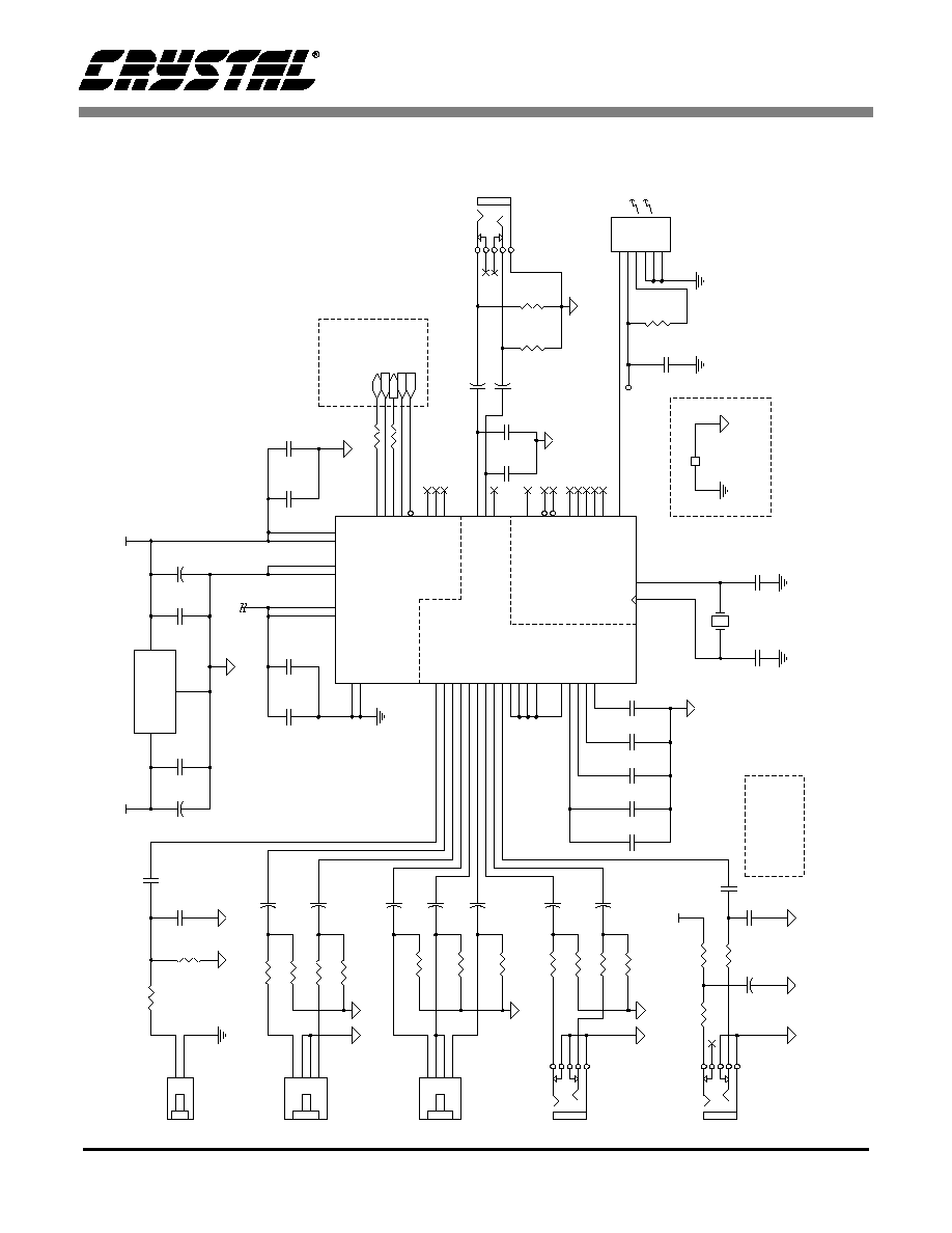
CS4205
DS489PP2
77
16. REFERENCE DESIGN
C17
10uF
EL
EC
+
R11
220k
C33
22pF
NP
O
C32
22pF
NP
O
C9
0.
1uF
X7
R
C23
1000pF
NP
O
R7
47
C22
0.
1uF
X7
R
C15
10uF
EL
EC
+
C11
0.
1uF
X7
R
J4
P
H
ON
O-
1
/
8
4
3
5
2
1
C3
EL
EC
+
C5
0.
1uF
X7
R
U1
M
C
78M
05A
CDT
OU
T
3
GND
2
IN
1
C4
0.
1uF
X7
R
C10
0.
1uF
X7
R
C6
10uF
EL
EC
+
C8
0.
1uF
X7
R
R8
47
R18
8.
2k
R13
220k
C24
1000pF
NP
O
C26
0.
1uF
X7
R
J6
TOTX
-
1
7
3
1
2
3
4
5
6
C21
2.
2uF
Z5
U
60 m
i
l
t
r
ac
e
GN
D
_
TI
E
Y1
24.
576 M
H
z
C25
1000pF
NP
O
C34
1000pF
NP
O
C35
1000pF
NP
O
U2
CS4205
LI
NE
_O
UT
_R
36
M
O
NO
_O
UT
37
AVdd2
38
GP
IO2
/
S
D
I1
39
GP
IO1
/
S
D
OU
T
44
GP
IO4
/
S
D
I3
41
AVss2
42
G
P
I
O
0/
LRCLK
43
GP
IO3
/
S
D
I2
40
ZS
C
L
K
34
ZS
D
A
TA
33
Z
L
RCLK
32
AF
L
T
3
31
DVdd1
1
XTL_IN
2
XTL_OUT
3
D
V
ss1
4
SD
AT
A_
O
U
T
5
BI
T
_
C
L
K
6
D
V
ss2
7
SD
AT
A_
I
N
8
SYN
C
10
DVdd2
9
R
ESET
#
11
PC
_
BEEP
12
PH
O
N
E
13
AU
X_
L
14
AU
X_
R
15
VI
D
E
O
_
L
16
VI
D
E
O
_
R
17
CD_L
18
CD_G
ND
19
CD_R
20
MI
C
1
21
MI
C
2
22
LI
NE
_I
N_L
23
LI
NE
_I
N_R
24
AVdd1
25
AVss1
26
R
E
FFL
T
27
V
r
ef
out
28
AF
L
T
1
29
AF
L
T
2
30
SPD
O
/
SD
O
2
48
EAPD
/
S
C
L
K
47
ID
1
#
46
ID
0
#
45
LI
NE
_O
UT
_L
35
C28
0
.
1uF
X7
R
R10
100k
J3
4X
1HDR-
A
U
1
2
3
4
C19
10uF
EL
EC
+
R6
6.
8k
C30
10uF
EL
EC
+
R9
100k
C1
0.
1uF
X7
R
C29
0.
1uF
X7
R
R2
4.
7k
R12
100k
R21
1
.
5
k
R19
2
.
2
k
R15
6
.
8
k
J1
2X
1HDR-
S
N/
P
B
1
2
R1
47k
R17
6
.
8
k
C12
10uF
EL
EC
+
C2
2700pF
X7
R
C7
10uF
EL
EC
+
C20
10uF
EL
EC
+
R4
6.
8k
R3
6.
8k
R14
6
.
8
k
J5
P
H
ON
O-
1
/
8
4
3
5
2
1
R16
6
.
8
k
C13
10uF
EL
EC
+
C14
10uF
EL
EC
+
C16
10uF
EL
EC
+
R5
6.
8k
J2
4X
1HDR-
A
U
1
2
3
4
R20
100
J7
P
H
ON
O-
1
/
8
4
3
5
2
1
DG
ND
AG
N
D
DG
ND
AG
N
D
+5V
A
+12V
AG
N
D
AG
N
D
+3.
3
V
D
DG
ND
DG
ND
+5V
D
DG
ND
AG
N
D
DG
ND
AG
N
D
AG
N
D
AG
N
D
AG
N
D
AG
N
D
AG
N
D
+5V
A
DG
ND
AG
N
D
AG
N
D
AG
N
D
AG
N
D
AG
N
D
ASYN
C
AR
ST
#
ABI
T
C
L
K
ASD
O
U
T
ASD
I
N
LI
N
E
OU
T
JA
CK
S/
PD
I
F
OU
T
PC
I
Audi
o C
ont
r
o
l
l
er
or
I
C
H
C
ont
r
o
l
l
er
(
50 P
P
M
)
T
i
e at
one poi
nt
onl
y
under
t
he c
odec
AC LINK
MIC IN
CD IN
M
I
C
IN
-3
d
B
ro
ll-o
f
f
f
r
equenci
e
s at
60 H
z
.
and 16 KH
z i
n
accor
dance w
i
t
h
PC
-
9
9
PC
SPEAKER
IN
L
I
NE
IN
AU
X I
N
10uF
Figure 3
5
. CS42
05
R
e
f
eren
ce
Des
i
gn

CS4205
78
DS489PP2
17. REFERENCES
1) Cirrus Logic, Audio Quality Measurement Specification, Version 1.0, 1997
http://www.cirrus.com/products/papers/meas/meas.html
2) Cirrus Logic, AN18: Layout and Design Rules for Data Converters and Other Mixed Signal Devices,
Version 6.0, February 1998
3) Cirrus Logic, AN22: Overview of Digital Audio Interface Data Structures, Version 2.0, February 1998
4) Cirrus Logic, AN134: AES and S/PDIF Recommended Transformers, Version 2, April 1999
5) Cirrus Logic, AN165: CS4297A/CS4299 EMI Reduction Techniques, Version 1.0, September 1999
6) Intel
Æ
, Audio Codec '97 Component Specification, Revision 2.1, May 1998
http://developer.intel.com/ial/scalableplatforms/audio/index.htm
7) Microsoft
Æ
, PC 99 System Design Guide, Version 1.0, July 1999
http://www.microsoft.com/hwdev/desguid/
8) Microsoft
Æ
, PC 2001 System Design Guide, Version 0.9, August 2000
http://www.pcdesguide.org/pc2001/default.htm
9) Intel
Æ
82801AA (ICH) and 82801AB (ICH0) I/O Controller Hub, June 1999
http://developer.intel.com/design/chipsets/datashts/290655.htm4
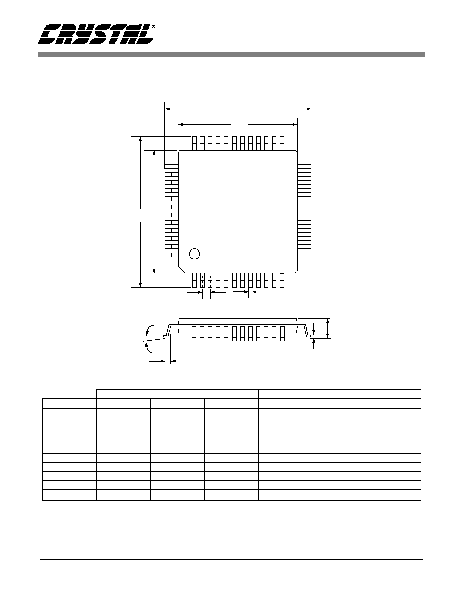
CS4205
DS489PP2
79
18. PACKAGE DIMENSIONS
INCHES
MILLIMETERS
DIM
MIN
NOM
MAX
MIN
NOM
MAX
A
---
0.055
0.063
---
1.40
1.60
A1
0.002
0.004
0.006
0.05
0.10
0.15
B
0.007
0.009
0.011
0.17
0.22
0.27
D
0.343
0.354
0.366
8.70
9.0 BSC
9.30
D1
0.272
0.28
0.280
6.90
7.0 BSC
7.10
E
0.343
0.354
0.366
8.70
9.0 BSC
9.30
E1
0.272
0.28
0.280
6.90
7.0 BSC
7.10
e*
0.016
0.020
0.024
0.40
0.50 BSC
0.60
L
0.018
0.24
0.030
0.45
0.60
0.75
0.000∞
4∞
7.000∞
0.00∞
4∞
7.00∞
* Nominal pin pitch is 0.50 mm
Controlling dimension is mm.
JEDEC Designation: MS022
48L LQFP PACKAGE DRAWING
E1
E
D1
D
1
e
L
B
A1
A