 | –≠–ª–µ–∫—Ç—Ä–æ–Ω–Ω—ã–π –∫–æ–º–ø–æ–Ω–µ–Ω—Ç: CS4216-KL | –°–∫–∞—á–∞—Ç—å:  PDF PDF  ZIP ZIP |
Features
∑
∑
CMOS Stereo Audio Input/Output System
Delta-Sigma A/D Converters
Delta-Sigma D/A Converters
Input Anti-Aliasing and Output
Smoothing Filters
Programmable Input Gain and
Output Attenuation
∑
∑
Sample Frequencies of 4 kHz to 50 kHz
∑
∑
CD Quality Noise and Distortion
< 0.01 %THD
∑
∑
Internal 64X Oversampling
∑
∑
Low Power Dissipation: 80 mA
1 mA Power-Down Mode
General Description
The CS4216 Stereo Audio Codec is a monolithic
CMOS device for computer multimedia, automotive,
and portable audio applications. It performs A/D and
D/A conversion, filtering, and level setting, creating 4
audio inputs and 2 audio outputs for a digital computer
system. The digital interfaces of left and right channels
are multiplexed into a single serial data bus with word
rates up to 50 kHz per channel. Up to 4 CS4216 de-
vices can be attached to a single hardware bus.
Both the ADCs and the DACs use delta-sigma modula-
tion with 64X oversampling. The ADCs include a digital
decimation filter which eliminates the need for external
anti-aliasing filters. The DACs include output smoothing
filters on-chip.
Ordering Information:
CS4216-KL
0
∞
to 70
∞
C
44-pin PLCC
CS4216-KQ
0
∞
to 70
∞
C
44-pin TQFP
CDB4216
Evaluation Board
16-Bit Stereo Audio Codec
Semiconductor Corporation
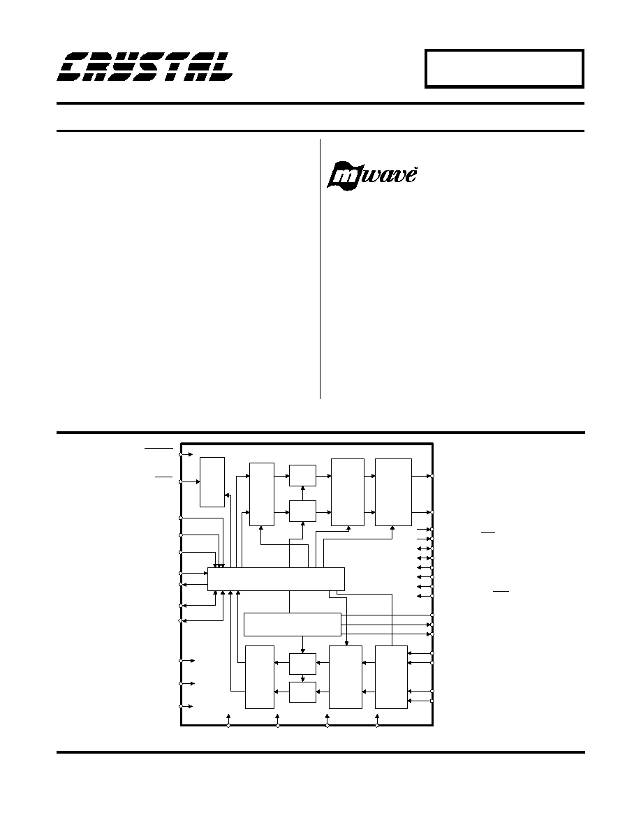
CS4216
S S Y N C
L O U T
R O U T
DI
GI
T
A
L
FI
LT
E
R
S
S E R IA L IN T E R F A C E C O N T R O L
DI
GI
T
A
L
FI
LT
E
R
S
INPUT
MUX
V O L T A G E R E F E R E N C E
C L K IN
M F 7:S F S 1 /F 2
M F 8:S F S 2 /F 3
S D IN
S D O U T
S C L K
S M O D E 1
R E S E T
R E F G N D
R E F B Y P
R E F B U F
L IN 1
L IN 2
R IN 1
R IN 2
V D
VA
D G N D
A G N D
A /D
A /D
D /A
D /A
D O 1
M F 5 :D O 2 /IN T
M F 2 :D O 3 /F 2 /C D IN
M F 1 :D O 4 /F 1 /C D O U T
D I1
M F 6 :D I2 /F 1
M F 3 :D I3 /F 3 /C C L K
OUTPUT
MUTE
OUT
P
UT
ATT
E
N
U
AT
I
O
N
INPUT
GAIN
P D N
S M O D E 2
S M O D E 3
PO
W
E
R
CONT
RO
L
M F 4 :D I4 /M A /C C S
Oct '93
DS83F2
1
Crystal Semiconductor Corporation
P.O. Box 17847, Austin, TX 78760
(512) 445-7222 FAX: (512) 445-7581
Copyright
©
Crystal Semicondutor Corporation 1993
(All Rights Reserved)
The CS4216 is an Mwave
TM
audio codec.

ANALOG CHARACTERISTICS
( T
A
= 25
∞
C; VA, VD = +5V; Input Levels: Logic 0 = 0V,
Logic 1 = VD; 1 kHz Input Sine Wave; CLKIN = 24.576 MHz; SM1; Conversion Rate = 48 kHz; SCLK =
12.288 MHz; Measurement Bandwidth is 10 Hz to 20 kHz; Unless otherwise specified.)
Parameter *
Symbol
Min
Typ
Max
Units
Analog Input Characteristics
- Minimum gain setting (0 dB); unless otherwise specified.
ADC Resolution
16
-
-
Bits
ADC Differential Nonlinearity
(Note 1)
-
-
±
0.9
LSB
Instantaneous Dynamic Range
IDR
80
85
-
dB
Total Harmonic Distortion
THD
-
-
0.01
%
Interchannel Isolation
-
80
-
dB
Interchannel Gain Mismatch
-
-
±
0.5
dB
Frequency Response
(Note 1)
-0.5
-
+0.2
dB
Programmable Input Gain Span
21
22.5
24
dB
Gain Step Size
-
1.5
-
dB
Absolute Gain Step Error
-
-
0.75
dB
Gain Drift
-
100
-
ppm/
∞
C
Offset Error
DC Coupled Inputs
-
±
10
±
100
LSB
AC Coupled Inputs
-
±
150
±
400
LSB
Full Scale Input Voltage
2.5
2.8
3.1
Vpp
Input Resistance
(Notes 1,2)
20
-
-
k
Input Capacitance
(Note 1)
-
-
15
pF
Notes:
1. This specification is guaranteed by characterization, not production testing.
2. Input resistance is for the input selected. Non-selected inputs have a very high (>1M
) input resistance.
* Parameter definitions are given at the end of this data sheet.
Mwave
TM
is a trademark of the IBM Corporation.
Specifications are subject to change without notice.
RECOMMENDED OPERATING CONDITIONS
(AGND, DGND = 0V, all voltages with re-
spect to 0V.)
Parameter
Symbol
Min
Typ
Max
Units
Power Supplies:
Digital
VD
4.75
5.0
5.25
V
Analog
VA
4.75
5.0
5.25
V
Operating Ambient Temperature
TA
0
25
70
∞
C
CS4216
2
DS83F2

ANALOG CHARACTERISTICS
(Continued)
Parameter *
Symbol
Min
Typ
Max
Units
Analog Output Characteristics
- Minimum Attenuation; Unless Otherwise Specified.
DAC Resolution
16
-
-
Bits
DAC Differential Nonlinearity
(Note 1)
-
-
±
0.9
LSB
Total Dynamic Range
TDR
-
93
-
dB
Instantaneous Dynamic Range
IDR
80
83
-
dB
Total Harmonic Distortion
(Note 4)
THD
-
-
0.02
%
Interchannel Isolation
(Note 4)
-
80
-
dB
Interchannel Gain Mismatch
-
-
±
0.5
dB
Frequency Response
(Note 1)
-0.5
-
+0.2
dB
Programmable Output Attenuation Span
(Note 3)
-45
-46.5
-
dB
Attenuation Step Size
(Note 3)
-
1.5
-
dB
Absolute Attenuation Step Error
(Note 3)
-
-
0.75
dB
Gain Drift
-
100
-
ppm/
∞
C
REFBUF Output Voltage
(Note 5)
1.9
2.2
2.5
V
Maximum output current= 400
µ
A
Offset Voltage
-
10
-
mV
Full Scale Output Voltage
(Note 4)
2.5
2.8
3.1
Vpp
Deviation from Linear Phase
(Note 1)
-
-
1
Degree
Out of Band Energy
(22 kHz to 100 kHz)
-
-60
-
dB
Power Supply
Power Supply Current
(Note 6)
Operating
-
80
100
mA
Power Down
-
-
1
mA
Power Supply Rejection
(1 kHz)
-
40
-
dB
Notes:
3. Tested in SM3, Slave sub-mode, 128 BPF.
4. 10 k
, 100 pF load.
5. REFBUF load current must be DC. To drive dynamic loads, REFBUF must be buffered.
AC variations in REFBUF current may degrade ADC and DAC performance.
6. Typically current: VA = 30mA, VD = 50mA. Power supply current does not include output loading.
* Parameter definitions are given at the end of this data sheet.
CS4216
DS83F2
3

SWITCHING CHARACTERISTICS
(T
A
= 25
∞
C; VA, VD = +5V, outputs loaded with 30 pF; Input
Levels: Logic 0 = 0V, Logic 1 = VD)
Parameter
Symbol
Min
Typ
Max
Units
Input clock (CLKIN) frequency
SM1:
CLKIN
2.048
24.576
25.6
MHz
SM2, SM3, SM4:
CLKIN
1.024
12.288
12.8
MHz
CLKIN low time
tckl
15
-
-
ns
CLKIN high time
tckh
15
-
-
ns
Sample Rate
(Note 1)
Fs
4
-
50
kHz
DI pins setup time to SCLK edge
(Note 1)
ts2
10
-
-
ns
DI pins hold time from SCLK edge
(Note 1)
th2
8
-
-
ns
DO pins delay from SCLK edge
tpd2
30
-
-
ns
SCLK and SSYNC output delay
Master Mode (Note 1)
tpd3
-
-
50
ns
from CLKIN rising
SCLK period
Master Mode (Note 7)
tsckw
-
1/(Fs*bpf)
-
s
Slave Mode
75
-
-
ns
SCLK high time
Slave Mode
tsckh
30
-
-
ns
SCLK low time
Slave Mode
tsckl
30
-
-
ns
SDIN, SSYNC setup time to SCLK edge
Slave Mode
ts1
15
-
-
ns
SDIN, SSYNC hold time from SCLK edge
Slave Mode
th1
10
-
-
ns
SDOUT delay from SCLK edge
tpd1
-
-
28
ns
Output to Hi-Z state
bit 64 (Note 1)
thz
-
-
12
ns
Output to non-Hi-Z
bit 1 (Note 1)
tnz
15
-
-
ns
RESET pulse width low
500
-
-
ns
CCS low to CCLK rising
SM4 (Note 1)
tcslcc
25
-
-
ns
CDIN setup to CCLK falling
SM4 (Note 1)
tdiscc
15
-
-
ns
CCLK low to CDIN invalid (hold time)
SM4 (Note 1)
tccdih
10
-
-
ns
CCLK high time
SM4 (Note 1)
tcclhh
25
-
-
ns
CCLK low time
SM4 (Note 1)
tcclhl
25
-
-
ns
CCLK Period
SM4 (Note 1)
tcclkw
75
-
-
ns
CCLK rising to CDOUT data valid
SM4 (Note 1)
tccdov
-
-
30
ns
CCLK rising to CDOUT Hi-Z
SM4 (Note 1)
tccdot
-
-
30
ns
CCLK falling to CCS high
SM4 (Note 1)
tcccsh
0
-
-
ns
Notes:
7. When the CS4216 is in master mode (SSYNC and SCLK outputs), the SCLK duty cycle is 50%.
The equation is based on the selected sample frequency (Fs) and the number of bits per frame (bpf).
CS4216
4
DS83F2

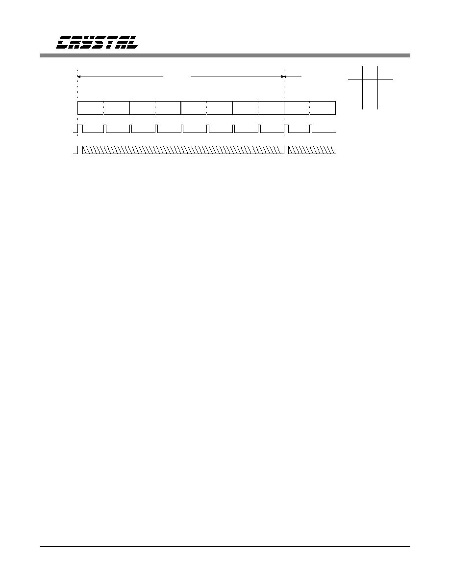
t nz
* Optional
Bit 1
Bit 2
Bit 1
Bit 2
Frame Sync
t sckl t sckh
t s1
t h1
t sckw
t sckh t sckl
t h1
t s1
t s1
t h1
SSYNC
[SM1, SM2\
SCLK
[SM1,SM2\
SCLK
[SM3,SM4\
SSYNC
[SM3,SM4\
SDIN
SDOUT
t pd1
t pd1
[SM1,SM2,SM3\
(SM4)
[SM1,SM2,SM3\
(SM4)
*Word Sync
t hz
*Word Sync
Bit 63
Bit 64
Bit 63
Bit 64
(Bit 32)
(Bit 31)
(Bit 31)
(Bit 32)
Bit 33
Bit 33
(Bit 1)
(Bit 1)
t s1
t h1
Bit 32
(Bit 32)
Bit 32
(Bit 32)
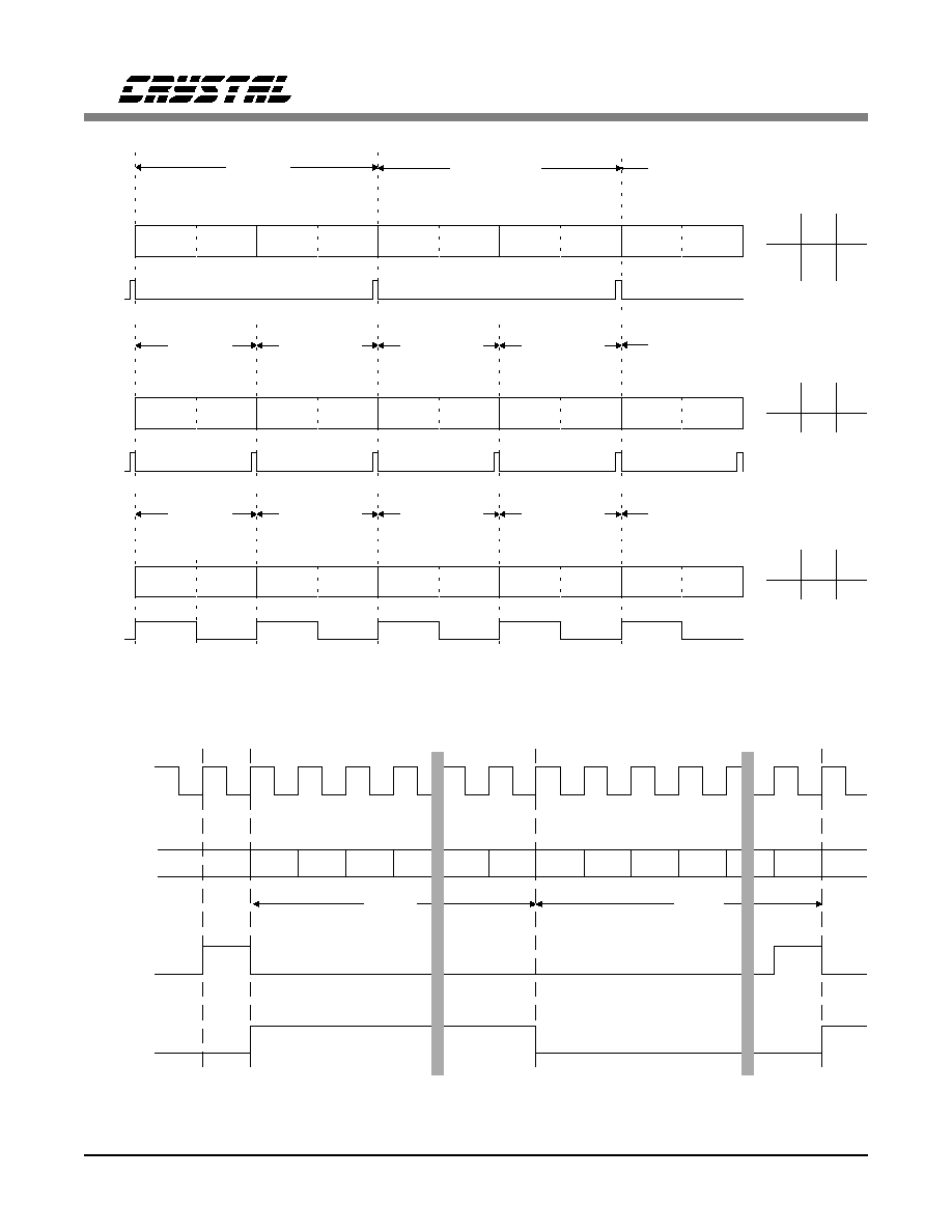
Serial Audio Port Timing
M F 3 :C C L K
M F 1 :C D O U T
M F 2 :C D IN
M F 4 :C C S
t ccdov
0
M S K
D O 1
t ccdih
t discc
1
2
3
5
8
9
4
6
7
10
A D V
L C L
11
L A tt4
L A tt3
L A tt2
L A tt1
L A tt0
R A tt4
R A tt3
R A tt2
t cclkl
t cclkh
t cslcc
t cclkw
M F 3 :C C L K
M F 1 :C D O U T
M F 2 :C D IN
M F 4 :C C S
t ccdot
24
28
29
32
31
30
27
26
25
23
22
R G a in 2 R G ain 1
0
0
1
R G ain 0
Err1
Err0
L C L
R C L
D I1
0
0
0
0
0
0
0
0
A D V
t cccsh
Serial Mode 4. Control Data Serial Port Timing
CS4216
DS83F2
5

DIGITAL CHARACTERISTICS
(T
A
= 25
∞
C; VA, VD = 5V)
Parameter
Symbol
Min
Typ
Max
Units
High-level Input Voltage
VIH
VD-1.0
-
-
V
Low-level Input Voltage
VIL
-
-
1.0
V
High-level Output Voltage at I0 = -2.0 mA
VOH
VD-0.3
-
-
V
Low-level Output Voltage at I0 = +2.0 mA
VOL
-
-
0.1
V
Input Leakage Current
(Digital Inputs)
-
-
10
µ
A
Output Leakage Current
(High-Z Digital Outputs)
-
-
10
µ
A
Output Capacitance
COUT
-
-
15
pF
Input Capacitance
CIN
-
-
15
pF
SCLK*
t s2 th2
t pd2
DIx
DOx
* SCLK is inverted for SM1 and SM2
DI/DO Timing
CLKIN
t ckl
SCLK
SCLK & SSYNC Output Timing
SSYNC
t ckh
t pd3
(Master Mode)
(Master Mode)
CS4216
6
DS83F2

A/D Decimation Filter Characteristics
Parameter
Symbol
Min
Typ
Max
Units
Passband
(Fs is conversion freq.)
0
-
0.45Fs
Hz
Frequency Response
-0.5
-
+0.2
dB
Passband Ripple
-
-
±
0.2
dB
Transition Band
0.45Fs
-
0.55Fs
Hz
Stop Band
0.55Fs
-
-
Hz
Stop Band Rejection
80
-
-
dB
Group Delay
-
16/Fs
-
s
Group Delay Variation vs. Frequency
-
0.0
µ
s
D/A Interpolation Filter Characteristics
Parameter
Symbol
Min
Typ
Max
Units
Passband
(Fs is conversion freq.)
0
-
0.45Fs
Hz
Frequency Response
-0.5
-
+0.2
dB
Passband Ripple
-
-
±
0.1
dB
Transition Band
0.45Fs
-
0.55Fs
Hz
Stop Band
0.55Fs
-
-
Hz
Stop Band Rejection
74
-
-
dB
Group Delay
-
16/Fs
-
s
Group Delay Variation vs. Frequency
-
-
0.1/Fs
µ
s
ABSOLUTE MAXIMUM RATINGS
(AGND, DGND = 0V, all voltages with respect to 0V.)
Parameter
Symbol
Min
Typ
Max
Units
Power Supplies:
Digital
VD
-0.3
-
6.0
V
Analog
VA
-0.3
-
6.0
V
Input Current
(Except Supply Pins)
-
-
±
10.0
mA
Analog Input Voltage
-0.3
-
VA+0.3
V
Digital Input Voltage
-0.3
-
VD+0.3
V
Ambient Temperature
(Power Applied)
-55
-
+125
∞
C
Storage Temperature
-65
-
+150
∞
C
Warning:
Operation beyond these limits may result in permanent damage to the device.
Normal operation is not guaranteed at these extremes.
CS4216
DS83F2
7
0 .1
µ
F
2.0
1
µ
F
0 .1
µ
F
+
24
4
V A
V D
23
5
+5 V
S up p ly
1
µ
F
+
CS4216
A G N D
D G N D
M F3 :D I3 /F 3 /C C L K
M F6 :D I2/F 1
M F1 :D O 4 /F 1 /C D O U T
M F2 :D O 3 /F 2 /C D IN
36
35
34
40
39
38
M F5 :D O 2 /IN T
M F 4 :D I4/M A /C C S
P a ralle l B its
S ub -M o d e
or
S etting s
or
C o n tro l P o rt
D I1
D O 1
33
37
R IN 2
26
L in e In 2
R ig ht
F e rrite B ea d
N o te : A G N D an d D G N D p in s M U S T be o n th e sam e gro un d p lan e
+
40 k
40 k
R O U T
LO U T
15
16
R E F B Y P
21
0 .1
µ
F
+
1 0
µ
F
R E FG N D
22
+
> 1.0
µ
F
> 1.0
µ
F
0 .0 0 2 2
µ
F
N P O
600
0 .0 0 2 2
µ
F
N P O
600
R ig ht
A u d io
O u tpu t
L eft
A u d io
O u tpu t
P D N
S D O U T
S C LK
S S Y N C
R E S E T
S D IN
2
13
42
44
1
43
C o n tro lle r
C L K IN
3
M F7 :S FS 1
M F8 :S FS 2
S M O D E 1
31
30
29
M o d e
S e ttin g
32
S M O D E 2
41
S M O D E 3
LIN 2
28
L in e In 2
L e ft
R IN 1
25
L in e In 1
R ig h t
R E F B U F
20
0 .4 7
µ
F
T o O p tio n al
In pu t B uffe rs
LIN 1
27
L in e In 1
L e ft
+ 5 V
A na log
If a s ep a ra te + 5 V
A na lo g su p p ly is u se d, re m o ve
the 2.0 o hm re sisto r
S e e
A na lo g Inp u ts se ctio n
for su gg ested inp u t ciruits.
R efe r to the
A n a log In p u ts
se ctio n fo r te rm in atin g
u nu se d lin e inp uts.
A ll o the r u n u se d in p uts
sh o uld b e tied to G N D . A ll N C
p in s sh ou ld be le ft floa ting .
Figure 1. Typical Connection Diagram
CS4216
8
DS83F2

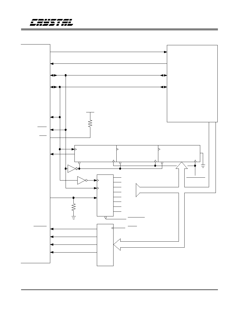
OVERVIEW
The CS4216 contains two analog-to-digital con-
verters, two digital-to-analog converters,
adjustable input gain, and adjustable output level
control. Since the converters contain all the re-
quired filters in digital or sampled analog form,
the filters' frequency responses track the sample
rate of the CS4216. Only a single-pole RC filter
is required on the analog inputs and outputs. The
RC filter acts as a charge reserve for the
switched-capacitor input and buffers op-amps
from a switched-capacitor load. Communication
with the CS4216 is via a serial port, with sepa-
rate pins for data into the device, and data from
the device. The filters and converters operate
over a sample rate range of 4 kHz to 50 kHz.
FUNCTIONAL SPECIFICATIONS
Analog Inputs and Outputs
Figure 1 illustrates the suggested connection dia-
gram to obtain full performance from the
CS4216. The line level inputs, LIN1 or LIN2
and RIN1 or RIN2, are selected by an internal
input multiplexer. This multiplexer is a source
selector and is not designed for switching be-
tween inputs at the sample rate.
Unused analog inputs that are not selected have
a very high input impedance, so they may be
tied to AGND directly. Unused analog inputs
that are selected should be tied to AGND
through a 0.1
µ
F capacitor. This prevents any
DC current flow.
The analog inputs are single-ended and inter-
nally biased to the REFBUF voltage (nominally
2.2 V). The REFBUF output pin can be used to
level shift an input signal centered around
0 Volts as shown in Figure 2. The input buffers
shown have a gain of 0.5, yielding a full scale
input sensitivity of 2 V
rms
with the CS4216 pro-
grammable gain set to 0. If the source imped-
ance is very low, then the inputs can be AC
coupled with a series 0.47
µ
F capacitor, elimi-
nating the need for external op-amps (see Figure
3). However, the use of AC coupling capacitors
will increase DC offset at 0dB gain (see Analog
Characteristics Table).
The analog outputs are also single-ended and
centered around the REFBUF pin. AC coupling
capacitors of >1
µ
F are recommended.
Line In
Right
Example
Op-Amps
are
MC34072
or
LT1013
Line In
Left
Op-amps are run
from VA+5V and
AGND
RINx
(PLCC pin 25 or 26)
REFBUF
LINx
(PLCC pin 27 or 28)
_
+
_
+
56 pF
10 k
20 k
0.47 uF
0.47 uF
0.47 uF 20 k
150
5 k
56 pF
10 k
150
0.01 uF
NPO
0.01 uF
NPO
Figure 2. DC Coupled Input.
Line In
Right
Line In
Left
0.01 uF
NPO
0.01 uF
NPO
150
150
0.47 uF
0.47 uF
RINx
(PLCC pin 25 or 26)
LINx
(PLCC pin 27 or 28)
Figure 3. AC Coupled Input
CS4216
DS83F2
9

Offset Calibration
Both input and output offset voltages are mini-
mized by internal calibration. Offset calibration
occurs after exiting a reset or power down condi-
tion. During calibration, which takes 194 frames,
output data from the ADCs will be all zeros, and
will be flagged as invalid. Also, the DAC outputs
will be muted. After power down mode or power
up, RESET should be held low for a minimum
of 50 ms to allow the voltage reference to settle.
Input Gain and Output Level Setting
Input gain is adjustable from 0 dB to +22.5 dB
in 1.5 dB steps. In serial modes SM1 and SM2,
the output level attenuation is adjustable from
0 dB to -22.5 dB. In serial modes SM3 and
SM4, the output level attenuation is adjustable
from 0 dB to -46.5 dB. Both input and output
gain adjustments are internally made on zero-
crossings of the analog signal, to minimize
"zipper" noise. The gain change automatically
takes effect if a zero crossing does not occur
within 512 frames.
Muting and the ADC Valid Counter
The mute function allows the output channels to
be silenced. It is the controlling processor's re-
sponsibility to reduce the signal level to a low
value before muting, to avoid an audible click.
The outputs should be muted before changing
the sample frequency.
The serial data stream contains a "Valid Data"
indicator for the A/D converters which is false
until enough clocks have passed since reset, or
low-power (power down mode) operation to have
valid A/D data from the filters, i.e., until calibra-
tion time plus the full latency of the digital
filters has passed.
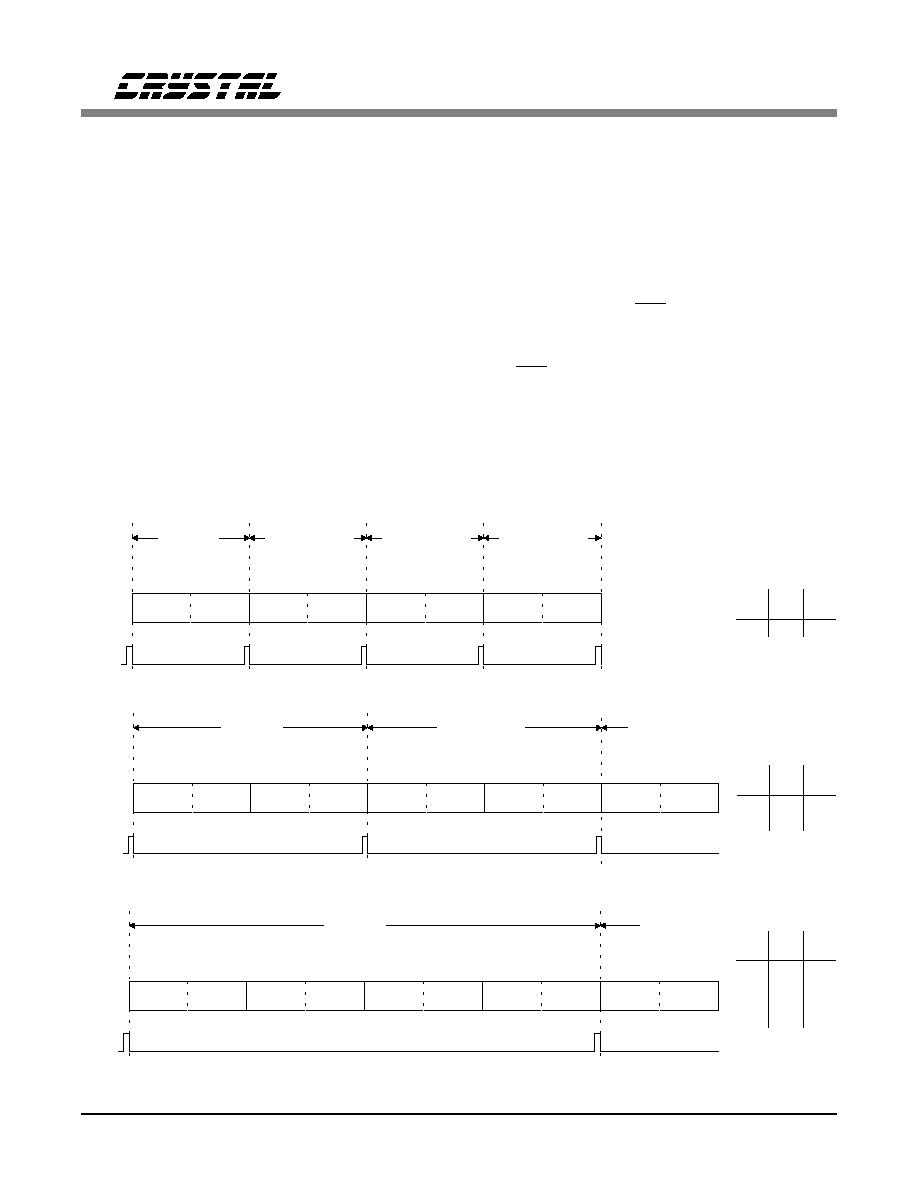
Parallel Digital Input/Output Pins
Parallel digital inputs are general purpose pins
whose value is reflected in the serial data output
stream to the processor. Parallel digital outputs
provide a way to control external devices using
bits in the serial data input stream. All parallel
digital pins, with the exception of DI1 and DO1,
are multifunction and are defined by the serial
mode selected. Serial modes 1 and 2 define all
multifunction pins as general purpose digital in-
puts and outputs. In Serial mode 3 only two
digital inputs and two digital outputs are avail-
able. In serial mode 4 only one digital input and
digital output exists. Figure 4 shows when the DI
pins are latched, and when the DO pins are up-
dated in SM3 and SM4.
Reset and Power Down Modes
Reset places the CS4216 into a known state and
must be held low for at least 50 ms after power-
up or a hard power down. Reset must also occur
when the codec is in master mode and a change
in sample frequency is desired. In reset, the digi-
tal outputs are driven low. Reset sets all control
data register bits to zero.
Hard power down mode may be initiated by
bringing the PDN pin low. All analog outputs
will be driven to the REFBUF voltage which
will then decay to zero. All digital outputs will
be driven low and then will go to a high imped-
ance state. Minimum power consumption will
occur if CLKIN is held low. After leaving the
power down state, RESET should be held low
for 50 ms to allow the analog voltage reference
to settle before calibration is started.
SSYNC
SCLK
DI pins
latched
DO pins
update
Start of
Frame
(SM3)
Figure 4. Digital Input/Output Timing
CS4216
10
DS83F2

Alternatively, soft power down may be initiated,
in slave mode, by reducing the SCLK frequency
below the minimum CLKIN/12. In soft power
down the analog outputs are muted and the serial
data from the codec will indicate invalid data
and the appropriate error code. The parallel bit
I/O is still functional in soft power down mode.
This is, in effect, a low power mode with only
the parallel bit I/O unit functioning.
Audio Serial Interface
In serial modes 1, 2, and 3, the audio serial port
uses 4 pins: SDOUT, SDIN, SCLK and SSYNC.
SDIN carries the D/A converters' input data and
control bits. Input data is ignored for frames not
allocated to the selected CS4216. SDOUT car-
ries the A/D converters' output data and status
bits. SDOUT goes to a high-impedance state
during frames not allocated to the selected
CS4216. SCLK clocks data in to and out of the
CS4216. The rising edge of SCLK clocks data
out on SDOUT. The falling edge latches data on
SDIN into the port (SCLK polarity is inverted in
Serial Modes 1&2). SSYNC indicates the start of
a frame and/or sub-frame. SCLK and SSYNC
must be synchronous to the master clock.
Serial mode 4 is similar to serial mode 3 with
the exception of the control information. In serial
mode 4 the control information is entered
through a separate asynchronous control port.
Therefore, the audio serial port only contains
audio data which reduces the number of bits on
the audio port from 64 to 32 per codec.
The serial port protocol is based on frames con-
sisting of 1, 2, or 4 sub-frames. The frame rate is
the system sample rate. Each sub-frame is used
by one CS4216 device. Up to 4 CS4216s may be
attached to the same serial control lines. SFS1
and SFS2 are tied low or high to indicate to each
CS4216 which sub-frame is allocated for it to
use.
Serial Data Format
In serial modes 1, 2, and 3, a sub-frame is
64 bits in length and consists of two 16-bit audio
values and two 16-bit control fields. In serial
mode 4 a sub-frame is 32 bits in length and only
contains the two 16-bit audio values; the control
data is loaded through a separate port. The audio
data is MSB first, 2's complement format. The
sub-frame bit assignments for serial modes 1, 2,
and 3, are numbered 1 through 64 and are shown
in Figures 5 and 6. Control data bits all reset to
zero.
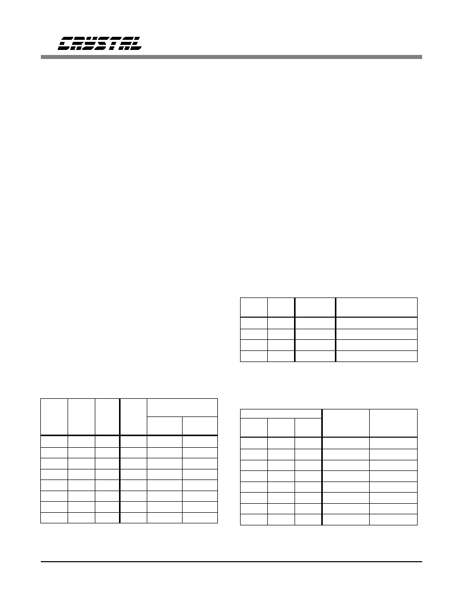
CS4216 SERIAL INTERFACE MODES
The CS4216 has 4 serial port modes, selected by
the SMODE1, SMODE2 and SMODE3 pins. In
all modes, CLKIN, SCLK and SSYNC must be
derived from the same clock source. SM1 is an
easy interface to ASICs that use a change in the
SCLK-to-CLKIN ratio to determine the sample
SMODE PINS
Serial
SCLK Bit
Sub-frame
Bits per
SCLK &
Master
3
2
1
Mode
Center
Width
Frame (BPF)
SSYNC
Frequency
0
0
0
SM1
Rising
64 bits
256
Slave
CLKIN = 512
◊
Fs
0
0
1
SM2
Rising
64 bits
256
Slave
SCLK = 256
◊
Fs
0
1
0
SM3
Falling
64 bits
64/128/256 Master/Slave
CLKIN/SCLK = 256
◊
Fs
0
1
1
Factory Test mode
1
x
x
SM4
Falling
32 bits
32/64/128
Master/Slave
CLKIN = 256
◊
Fs
Contains audio data only. Control information is entered through a separate serial port.
Table 1. Serial Port Modes
CS4216
DS83F2
11

*
Sub-frame Bits 17 to 24
17
18
19
20
21
22
23
24
0
0
0
0
EXP MUTE
ISL
ISR
EXP
Expand bit
Reserved. Must be set to zero.
MUTE Mute D/A Outputs
0 - Normal Outputs
1 - Mute Outputs
ISL
Select Left Input Mux
0 - Select LIN1
1 - Select LIN2
ISR
Select Right Input Mux
0 - Select RIN1
1 - Select RIN2
INPUT DATA BIT DEFINITIONS
Sub-frame bits 1 to 16
Left DAC Audio Data, MSB first, 2's comple-
ment coded.
Sub-frame Bits 25 to 32
25
26
27
28
29
30
31
32
LG3
LG2
LG1
LG0
RG3
RG2
RG1
RG0
LG3-LG0
Sets left input gain.
LG3 is the MSB. LG0 represents 1.5 dB.
0000 = no gain.
1111 = +22.5 dB gain
RG3-RG0 Sets right input gain.
RG3 is the MSB. RGO represents 1.5 dB.
0000 = no gain
Sub-frame Bits 51 to 60
51
52
53
54
55
56
57
58
59
60
LA4 LA3 LA2 LA1 LA0 RA4 RA3 RA2 RA1 RA0
0
0
LA3 LA2 LA1 LA0 RA3 RA2 RA1 RA0
LA4-LA0
Sets left output attenuation
RA4-RA0 Sets right output attenuation
*SM3,4
LA4 is the MSB.
00000 = no attenuation
11111 = -46.5 dB
SM1, 2
LA3 is the MSB.
0000 = no attenuation
1111 = -22.5 dB
LA0 represents 1.5 dB.
SM1, 2
RA3 is the MSB.
0000 = no attenuation
1111 = -22.5 dB
*SM3,4
RA4 is the MSB.
00000 = no attenuation
11111 = -46.5 dB
RA0 represents 1.5 dB.
Sub-frame Bits 61 to 64
61
62
63
64
DO1
DO2
DO3
DO4
DO1-DO4
Set the logic level on the 4 digital output
pins. In SM3 DO3 and DO4 are not
available. In SM4 DO2, DO3, & DO4
are not available.
Sub-frame Bits 33 to 48
Right DAC audio data MSB first, 2's comple-
ment coded.
64
DAC - Left Word
0 0 0 0
Left
A/D Gain
3
0
Right
A/D Gain
3
0
M
In
Sel.
0 0 0 0
DAC - Right Word
Left
D/A Att.
3
0
Right
D/A Att.
3
0
DO
1
DO
2
DO
3
DO
4
Sub-frame
Word B
Word A
DAC - Left Word
0 0 0 0
Left
A/D Gain
3
0
Right
A/D Gain
3
0
EX
P
M
In
Sel.
SM1 and SM2
SM3
0 0
DAC - Right Word
Left
D/A Att.
4
0
Right
D/A Att.
4
0
DO
1
DO
2
X X
MS
B
LS
B
MS
B
LS
B
MS
B
LS
B
MSB
LS
B
01
16
17
21
24
25
28
29
32
22
23
33
52
48
53
56
57
60
61
51
55
EX
P
Sub-frame
Figure 5. Serial Data Input Format - SM1, SM2, and SM3.
Sub-frame Bits 49 to 50
Must be zero.
CS4216
12
DS83F2

Sub-frame Bits 17 to 24
17
18
19
20
21
22
23
24
RESERVED
0
ADV
LCL
RCL
ADV
ADC Valid data bit.
0 - Invalid ADC data
1 - Valid ADC data
Indicates ADC has completed initialization
after power-up, low power mode,
or mute.
LCL
Left ADC clipping indicator
0 - Normal
1 - Clipping
RCL
Right ADC clipping indicator
0 - Normal
1 - Clipping
RESERVED bits can be 0 or 1
Sub-frame Bits 25 to 32
25
26
27
28
29
30
31
32
ER3
ER2
ER1
ER0
Ver3
Ver2
Ver1
Ver0
ER3-ER0 Error Word
0000 - Normal ≠ No errors.
0001 - Input Sub-frame Bit 21 is set.
Control data will not be loaded
0010 - Sync Pulse is incorrect.
Causes the analog output to mute.
0011 - SCLK is outside the allowable
range. Analog output mutes.
Ver3-Ver0
CS4216 Version Number
0000 = "A" (see Appendix A)
0001 = "B", "C", . . . (This data sheet)
Sub-frame Bits 33 to 48
Right ADC Audio Data, MSB first, 2's comple-
ment coded.
Sub-frame Bits 1 to 16
Left ADC Audio Data, MSB first, 2's comple-
ment coded.
OUTPUT DATA BIT DEFINITIONS
64
ADC - Left Word
3
0 3
0
0
AD
V
ADC - Right Word
Sub-frame
Word B
Word A
ADC - Left Word
3
0 3
0
0
SM1 and SM2
SM3
ADC - Right Word
DI
1
DI
2
X X
MS
B
MS
B
LS
B
LS
B
AD
V
LC
L
RC
L
Error
Error
Version
Version
MS
B
MS
B
LS
B
LS
B
0 0 0 1 0 0 0 0
0 0 0 1 0 0 0 0
DI
1
DI
2
DI
3
DI
4
01
16
17
21
24
25
28
29
32
22
23
33
52
48
53
56
57
60
61
55
LC
L
RC
L
.X X X X
X X X X
X X X X
X X X X
Sub-frame
Figure 6. Serial Data Output Format - SM1, SM2, and SM3.
Sub-frame Bits 49 to 60
These bits are reserved, and can be 0 or 1.
Sub-frame Bits 61 to 64
61
62
63
64
DI1
DI2
DI3
DI4
DI1-DI4
These bits follow the state of the Digital
Input pins. In SM3 DI3 and DI4 are used
and unavailable. In SM4 DI2, DI3, & DI4
are not available as input bits.
CS4216
DS83F2
13

frequency. SM2 is similar to SM1 except that
CLKIN is not used and SCLK becomes the mas-
ter clock and is fixed at 256
◊
Fs. SM3 was
designed as an easy interface to general purpose
DSPs and provides extra features such as one
more bit of attenuation, a master mode, and vari-
able frame sizes. SM4 is similar to SM3 but
splits the audio data from the control data
thereby reducing the audio serial bus bandwidth
by half. The control data is transmitted through a
control serial port in SM4.
Table 1 lists the serial port modes available,
along with some of the differences between
modes. The first three columns in Table 1 select
the serial mode. The "SCLK Bit Center" column
indicates whether SCLK is rising or falling in
the center of a bit period. The "Sub-frame
Width" column indicates how many bits are in
an individual codec's sub-frame. SM4 differs
from all other modes by separating the control
data from the audio data. In both SM1 and SM2,
there are 256 bits per frame which allows up to
four codecs to occupy the same bus. In SM3 and
SM4, the number of bits per frame is program-
mable. In SM1 and SM2, SCLK and SSYNC
must be generated externally; whereas, in SM3
and SM4 the CS4216 can optionally generate
those signals. In all modes, SCLK and SSYNC
must be synchronous to the master clock. The
last column in Table 1 lists the master frequency
used by the codec. In SM1, the master fre-
quency, input on CLKIN, is 512 times the
highest sample frequency available. In SM2, the
master frequency is fixed at 256 times the sam-
ple frequency and, in this mode, SCLK is the
master clock. In SM3, the master frequency is
256 times the highest frequency available and is
input on CLKIN or SCLK, based on the sub-
mode used. In SM4, the master frequency is also
256 times the highest frequency available and is
input on CLKIN.
SERIAL MODE 1, SM1
Serial Mode 1 is a slave mode selected by set-
ting SMODE3 = SMODE2 = SMODE1 = 0.
SCLK and SYNC must be synchronous the mas-
ter clock. SM1 uses a two bit wide (minimum)
frame sync with an optional word sync. In this
mode, SSYNC low for one SCLK period fol-
lowed by SSYNC high for a minimum of two
SCLK periods indicates the beginning of a
frame. The first bit of the frame starts with the
rising edge of SSYNC. An optional word sync,
being one SCLK period high, may be used to
indicate the start of a new 32-bit word. Figures 5
and 6 contain the serial data format for SM1. In
this serial mode, the ratio of two clocks are used
to select sample frequency. These are the master
clock CLKIN and the serial clock SCLK.
CLKIN should be set to 512
◊
Fs
max
, where
Fs
max
is the maximum required sample rate.
SCLK must be externally set to a value of
CLKIN/N, such that SCLK equals 256 times the
desired sample rate. The codec uses the ratio be-
tween CLKIN and SCLK to set the internal
sample frequency and causes the CS4216 to go
into soft power down mode if the SCLK fre-
quency drops to <CLKIN/12. Even if only 1
CS4216 is used, the timing for 4 devices must be
maintained. Table 2 shows some example sample
rates for SM1.
Sample Rate
SCLK
CLKIN
N
kHz
MHz
MHz
48
12.288
24.576
2
32
8.192
24.576
3
24
6.144
24.576
4
19.2
4.9152
24.576
5
16
4.096
24.576
6
12
3.072
24.576
8
9.6
2.4576
24.576
10
8
2.048
24.576
12
7.2
1.843
22.116
12
44.1
11.2896
22.5792
2
Table 2. SM1 - Example Clock Frequencies
CS4216
14
DS83F2
SERIAL MODE 2, SM2
Serial Mode 2 is enabled by setting SMODE3 =
SMODE2 = 0, and SMODE1 = 1. SM2 is simi-
lar to SM1 except that SCLK is fixed at 256
◊
Fs and is the master clock instead of CLKIN.
The CLKIN pin is ignored in this mode and
should be tied low. In SM2, the sample fre-
quency will scale linearly with the frequency of
SCLK. Up to four codecs may occupy the serial
bus since each codec requires only 64 bit periods
and a frame is fixed at 256 bit periods. The se-
rial data format is the same as SM1 and is
illustrated in Figures 5 and 6.
The multifunction pins in SM2 are defined iden-
tically to SM1. See Serial Mode 1, SM1 section
for more details.
SERIAL MODE 3, SM3
Se ria l M o d e 3 i s en ab l ed b y se tt in g
SMODE3 = 0, SMODE2 = 1 and SMODE1 = 0.
This mode is designed to interface easily to
DSPs and has the added versatility of a program-
mable number of bits per frame, a master mode,
and one extra bit of D/A attenuation. In SM3,
two of the parallel digital input bits and two of
the parallel digital output bits are available.
Master Clock Frequency
In SM3, the master clock, CLKIN, must be
256
◊
Fs
max
. For example, given a 48 kHz maxi-
mum sample frequency, the master clock
frequency must be 12.288 MHz. SCLK and
SSYNC must be synchronous to CLKIN.
D/A Attenuation
SM3 has one more bit per channel allocated for
D/A attenuation which doubles the attenuation
range. Figure 5 illustrates the serial data in,
SDIN, sub-frame for all SM3 sub-modes. The
upper portion of this figure shows modes SM1
and SM2 where the D/A attenuation is located in
Word B, bits 53 through 60. Four bits allow at-
tenuation on each channel from 0 dB down to
-22.5 dB using 1.5 dB steps. In SM3 the attenu-
ation bits are still located in Word B, but start at
bit 51 of the sub-frame. This allows five bits of
attenuation per channel instead of four, produc-
ing an attenuation range for each channel from
0 dB down to -46.5 dB.
In SM3 MF5:DO2 is a general purpose output
and MF6:DI2 is a general purpose input. The
other six multifunction pins are used to select
sub-modes under SM3.
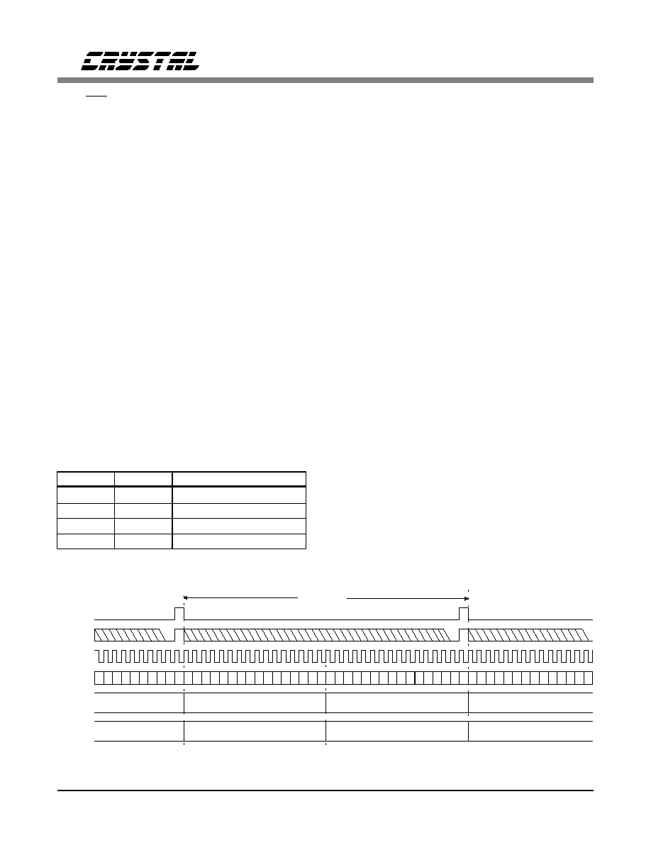
SM3 is divided into two sub-modes, Master and
Slave. In Master sub-mode, the CS4216 gener-
a t es SSYNC and SC LK, while in Sl ave
sub-mode SSYNC and SCLK must be generated
SFS2
SFS1
frame
0
0
1
1
0
1
0
1
1
2
3
4
Sub-frame 1
Sub-frame 2
Sub-frame 3
Sub-frame 4
FRAME (n+1)
Word A
Word B
Word A
Word B
Word A
Word B
Word A
Word B
FRAME n
Sub-frame 1
Word A
Word B
256 SCLK Periods
SSYNC
DATA
FS
WS
WS
WS
WS
WS
WS
WS
FS
WS
FS =
Frame Sync
Low followed by
Two High Bits
WS =
One High
Optional
Not Needed
or
SSYNC
MF8:
MF7:
Sub-
Figure 7. SM1, SM2 - 256 Bits per Frame.
CS4216
DS83F2
15

externally. In Master sub-mode, the serial port
signal transitions are controlled with respect to
the internal analog sampling clock to minimize
the amount of digital noise coupled into the ana-
log section. Since SSYNC and SCLK are
externally derived in Slave sub-mode, optimum
noise management cannot be obtained; therefore,
Master sub-modes should be used whenever pos-
sible.
Master Sub-Mode (SM3)
M as te r s u b - m o d e is s ele cte d b y s e tt in g
MF4:MA = 1, which configures SSYNC and
SCLK as outputs from the CS4216. During
power down, SSYNC and SCLK are driven high
impedance, and during reset they both are driven
low. In Master sub-mode the number of bits per
frame determines how many codecs can occupy
the serial bus and is illustrated in Figure 8.
Bits Per Frame (Master Sub-Mode)
MF8:SFS2 selects the number of bits per frame.
The two options are MF8:SFS2 = 1 which se-
lects 128 bits per frame, and MF8:SFS2 = 0
which selects 64 bits per frame.
Selecting 128 bits per frame (MF8:SFS2 = 1) al-
lows two CS4216s to operate from the same
serial bus since each codec requires 64 bit peri-
ods. The sub-frame used by an individual codec
is selected using MF7:SFS1. MF7:SFS1 = 0 se-
lects sub-frame 1 which is the first 64 bits
following the SSYNC pulse. MF7:SFS1 = 1 se-
lects sub-frame 2 which is the last 64 bits of the
frame.
Selecting 64 bits per frame (MF8:SFS2 = 0) al-
lows only one CS4216 to occupy the serial port.
Since there is only one sub-frame (which is
equal to one frame), MF7:SFS1 is defined differ-
ently in this mode. MF7:SFS1 selects the format
of SSYNC. MF7:SFS1 = 0 selects an SSYNC
pulse one SCLK period high, directly preceding
the data as shown in the center portion of Fig-
ure 8. This format is used for all other Master
and Slave sub-modes in SM3. If MF7:SFS1 = 1,
an alternate SSYNC format is chosen in which
SSYNC is high during the entire Word A
(32 bits), which includes the left sample, and
low for the entire Word B (32 bits), which in-
cludes the right sample. This alternate format for
SSYNC is illustrated in the bottom portion of
Figure 8 and is only available in Master sub-
mode with 64 bits per frame. A more detailed
timing diagram for the 64 bits-per-frame Master
sub-mode is shown in Figure 9.
Sample Frequency Selection (Master Sub-Mode)
In SM3, Master sub-mode, the multifunction
pins MF1:F1, MF2:F2, and MF3:F3 are used to
select the sample frequency divider. Table 3 lists
the decoding for the sample frequency select
pins where the sample frequency selected is
CLKIN/N. Also shown are the sample frequen-
cies obtained by using one of two example
ma ster clo ck s : either 12.288 MHz or
11.2896 MHz. The codec must be reset when
changing sample frequencies to allow the codec
to calibrate to the new sample frequency.
Slave Sub-Mode (SM3)
In SM3, Slave sub-mode is selected by setting
MF4:MA = 0 which configures SSYNC and
SCLK as inputs to the CS4216. These two sig-
nals must be externally derived from CLKIN. In
Slave sub-mode, the phase relationship between
SCLK/SSYNC and CLKIN cannot be controlled
since SCLK and SSYNC are externally derived.
Therefore, the noise performance may be slightly
worse than when using the master sub-mode.
The number of sub-frames on the serial port is
selected using MF1:F1 and MF2:F2. In Slave
sub-mode MF3:F3 works as a general purpose
input. Figures 10 through 12 illustrate the Slave
sub-mode formats.
CS4216
16
DS83F2
Sub-frame 1
Sub-frame 2
FRAME (n+2)
Word A
Word B
Word A
Word B
Sub-frame 1
Word A
Word B
FRAME n
128 SCLK Periods
Sub-frame 2
Word A
Word B
FRAME (n+3)
Sub-frame 1
Word A
Word B
Sub-frame 1
Word A
Word B
FRAME n
64 SCLK Periods
Sub-frame 1
Word A
Word B
FRAME (n+1)
Sub-frame 1
Word A
Word B
FRAME (n+2)
Sub-frame 1
Word A
Word B
FRAME (n+3)
Sub-frame 1
Word A
Word B
FRAME (n+4)
Sub-frame 1
Word A
Word B
FRAME n
64 SCLK Periods
Sub-frame 1
Word A
Word B
FRAME (n+1)
Sub-frame 1
Word A
Word B
FRAME (n+2)
Sub-frame 1
Word A
Word B
FRAME (n+3)
Sub-frame 1
Word A
Word B
FRAME (n+4)
SSYNC
DATA
SSYNC
DATA
SSYNC
DATA
SFS2
SFS1 frame
1
1
0
1
MF8:
MF7: Sub-
1
2
SFS2
SFS1 frame
0
0
MF8:
MF7: Sub-
1
SFS2
SFS1 frame
0
1
MF8:
MF7: Sub-
1
Figure 8. SM3, Master Sub-Mode.
MSB
SCLK
SSYNC
(MF7:SFS1=0)
SSYNC
(MF7:SFS1=1)
MSB
32 CLOCKS
32 CLOCKS
LSB
Word A
Word B
LSB
SDIN
SDOUT
Figure 9. Detailed Master Sub-Mode, 64 BPF.
CS4216
DS83F2
17
Bits per Frame (Slave Sub-Mode)
In Slave sub-mode, MF1:F1 and MF2:F2 select
the number of bits per frame which determines
how many CS4216's can occupy one serial port.
Table 4 lists the decoding for MF1:F1 and
MF2:F2.
When set for 64 SCLKs per frame, one device
occupies the entire frame; therefore, a sub-frame
is equ ivalen t to a frame. MF7 :SFS1 and
MF8:SFS2 must be set to zero. See Figure 10.
When set for 128 SCLKs per frame, two devices
can occupy the serial port, with MF7:SFS1 se-
lecting the particular sub-frame. MF8:SFS2 must
be set to zero. See Figure 11.
When set for 256 SCLKs per frame (MF1:F1,
MF2:F2 = 10), four devices can occupy the se-
rial port. In this format both MF8:SFS2 and
MF7:SFS1 are used to select the particular sub-
frame. See Figure 12.
In all three of the above Slave sub-mode for-
mats, the frequency of the incoming SCLK
signal, in relation to the master clock provided
on the CLKIN pin, determines the sample fre-
quency. The CS4216 determines the ratio of
SCLK to CLKIN and sets the internal operating
frequency accordingly. Table 5 lists the SCLK to
CLKIN frequency ratio used to determine the
codec's sample frequency. To obtain a given
sample frequency, SCLK must equal CLKIN di-
vided by the number in the table, based on the
number of bits per frame. As an example, assum-
in g 6 4 B P F ( b its per frame) and
CLKIN = 12.288 MHz, if a sample frequency of
24 kHz is desired, SCLK must equal CLKIN di-
vided by 8 or 1.536 MHz.
When MF1:F1 = MF2:F2 = 1, SCLK is used as
the master clock and is assumed to be 256 times
the sample frequency. In this mode, CLKIN is
ignored and the sample frequency is linearly
scaled with SCLK. (The CLKIN pin must be
tied low.) This mode also fixes SCLK at 256 bits
per frame with MF7:SFS1 and MF8:SFS2 select-
ing the particular sub-frame.
Fs (kHz)
MF1:
MF2:
MF3:
N
with CLKIN
F1
F2
F3
12.288
11.2896
MHz
MHz
0
0
0
256
48.00
44.10
0
0
1
384
32.00
29.40
0
1
0
512
24.00
22.05
0
1
1
640
19.20
17.64
1
0
0
768
16.00
14.70
1
0
1
1024
12.00
11.025
1
1
0
1280
9.60
8.82
1
1
1
1536
8.00
7.35
Table 3. SM3-Master, Fs Select
MF1:
MF2:
Bits per
Sample Frequency/
F1
F2
Frame
SCLK
0
0
64
ratio to CLKIN sensed
0
1
128
ratio to CLKIN sensed
1
0
256
ratio to CLKIN sensed
1
1
256
fixed
. = 256
◊
Fs
SCLK is master clock. CLKIN is not used.
Table 4. SM3-Slave, Bits per Frame.
SCLK to CLKIN Ratio
Fs (kHz)
Fs (kHz)
BPF
BPF
BPF
with CLKIN with CLKIN
256
128
64
12.288 MHz 11.2896 MHz
1
2
4
48.00
44.10
1.5
3
6
32.00
29.40
2
4
8
24.00
22.05
2.5
5
10
19.20
17.64
3
6
12
16.00
14.70
4
8
16
12.00
11.025
5
10
20
9.60
8.82
6
12
24
8.00
7.35
Table 5. SM3-Slave, Fs Select.
CS4216
18
DS83F2
SERIAL MODE 4, SM4
S e ri a l m o d e 4 i s en ab led b y s ett in g
SMODE3 = 1. Both Master and Slave sub-
modes are available and are selected by setting
the SMODE2 and SMODE1 pins as shown in
Table 6. In Master sub-mode, the phase relation-
ship between SCLK/SSYNC and CLKIN is
controlled to minimize digital noise coupling
into the analog section. Therefore, Master sub-
mo de m a y y ie ld sl ig h t ly b et te r no i se
performance than Slave sub-mode. In Slave sub-
mode, SCLK and SSYNC must be synchronous
to the master clock.
In serial mode 4, SM4, the CLKIN frequency
must be 256 times the highest sample frequency
needed. Also, SM4 has five attenuation bits for
each D/A output channel. SM4 differs from SM3
in that SM4 splits the audio data from the con-
trol data with the control data input on an
independent serial port. This reduces the audio
serial bus bandwidth in half, providing an easier
interface to low-cost DSPs. The audio serial port
sub-frame is illustrated in Figure 13 for SM4.
Interrupt Pin - MF5:INT
Serial Mode 4 also defines the multifunction pin
MF5:INT as an open-collector interrupt pin. In
SM4, this pin requires a pullup resistor and will
go low when the ADV bit or DI1 pin change, or
a rising edge on the LCL or RCL bits, or by
exiting an SCLK out of range condition (Er-
ror = 3). The interrupt may be masked by setting
the MSK bit in the control serial data port.
Sub-frame 1
FRAME (n+1)
Word A
Word B
Sub-frame 1
Word A
Word B
FRAME n
64 SCLK Periods
FRAME (n+2)
Sub-frame 1
Word A
Word B
FRAME (n+3)
Sub-frame 1
Word A
Word B
SSYNC
DATA
SFS2
SFS1 frame
0
0
1
MF8:
MF7:
Sub-
Figure 10. SM3-Slave - 64 BPF; MF1:F1, MF2:F2 = 00
Sub-frame 1
Sub-frame 2
FRAME (n+1)
Word A
Word B
Word A
Word B
Sub-frame 1
Word A
Word B
FRAME n
128 SCLK Periods
Sub-frame 2
Word A
Word B
FRAME (n+2)
Sub-frame 1
Word A
Word B
SSYNC
DATA
SFS2
SFS1 frame
0
0
0
1
1
2
MF8:
MF7:
Sub-
Figure 11. SM3-Slave - 128 BPF; MF1:F1, MF2:F2 = 01
S u b-fra m e 1
S u b-fram e 2
S u b-fram e 3
S u b-fra m e 4
F R A M E (n+ 1)
W ord A
W ord B
W o rd A
W ord B
W ord A
W ord B
W ord A
W ord B
F R A M E n
S ub-fra m e 1
W o rd A
W ord B
25 6 S C LK P erio ds
S S Y N C
D A T A
S F S 2
S F S 1 fram e
0
0
1
1
0
1
0
1
1
2
3
4
M F 8:
M F 7:
S u b-
Figure 12. SM3-Slave - 256 BPF; MF1:F1, MF2:F2 = 10
CS4216
DS83F2
19
MF5:INT is reset by reading the control serial
port.
Master Sub-Mode (SM4)
Master sub-mode configures SSYNC and SCLK
as outputs from the CS4216. During power
down, SSYNC and SCLK are driven high im-
pedance, and during reset they both are driven
low. There are two SM4 Master sub-modes. One
allows 32 bits per frame and the other allows 64
bits per frame. As shown in Table 6, the
SMODE1 and SMODE2 pins select the particu-
lar Master sub-mode (as well as the Slave
sub-mode). When SMODE1 is set to zero,
SMODE2 selects either Master sub-mode with
32-bit frames, or Slave sub-mode.
SMODE1,SMODE2 = 00 selects Master sub-
mode where a frame = sub-frame = 32 bits. This
sub-mode allows only one codec on the audio
serial bus, with the first 16 bits being the left
channel and the second 16 bits being the right
channel. The Applications of SM4 section con-
ta ins m or e i nf o r mat io n o n l ow - co s t
implementations of this sub-mode.
SMODE1 = 1 selects Master sub-mode with a
frame width of 64 bits. This sub-mode allows up
to two codecs to occupy the same bus. SMODE2
is now used to select the particular time slot. If
SMODE2 = 0 the codec selects time slot 1,
which is the first 32 bits. If SMODE2 = 1 the
codec selects time slot 2, which is the second
32 bits.
In Master sub-mode, multifunction pins MF6:F1,
MF7:F2, and MF8:F3 select the sample fre-
quency as shown in Table 7. This table indicates
how to obtain standard audio sample frequencies
g ive n one of two CLKIN frequencies:
12.288 MHz or 11.2896 MHz. Other CLKIN
frequencies may be used with the corresponding
sample frequencies being CLKIN/N. The codec
must be reset when changing sample frequencies
to allow a new calibration to occur.
Slave Sub-Mode (SM4)
In SM4, Slave sub-mode is selected by setting
SMODE1,SMODE2 = 01. This mode configures
SSYNC and SCLK as inputs to the CS4216.
These two signals must be externally derived
from CLKIN. Since the CS4216 has no control
over the phase relationship of SSYNC and
SMODE1
SMODE2
SM4, Sub-Mode
0
0
Master, 32 BPF
0
1
Slave, 128/64/32 BPF
1
0
Master, 64 BPF, TS1
1
1
Master, 64 BPF, TS2
Table 6. SM4 Sub-Modes.
SSYNC
SCLK
SDIN
SDOUT
Sub-Fram e
16
17
32
1
1
8
9
24
25
32
14
23
AD C - Left W ord
MS
B
LSB
AD C - R ight W ord
MS
B
LSB
AD C - Left W ord
MS
B
AD C - R ight W ord
LSB
D AC - Left W ord
MS
B
LSB
D A C - R ight W ord
MS
B
LS
B
D AC - Left W ord
MS
B
D AC - R ight W ord
LSB
(slave)
(m aster)
Figure 13. SM4-Audio Serial Port, 32 BPF
CS4216
20
DS83F2

SCLK to CLKIN, the noise performance in
Slave sub-mode may be slightly worse than
when using Master sub-mode. The CS4216 inter-
nally sets the sample frequency by sensing the
ratio of SCLK to CLKIN; therefore, for a given
CLKIN frequency, the sample frequency is se-
lected by changing the SCLK frequency.
SM4-Slave allows up to four codecs to occupy
the same audio serial port. Table 8 lists the pin
configurations required to set the serial audio
port up for 32, 64, or 128 bits-per-frame (BPF).
Since each codec requires one sub-frame of
32 bits, 64 bits-per-frame allows up to two
codecs to occupy the same audio serial port, and
128 bits-per-frame allows up to four codecs to
occupy the same audio serial port. When set up
for more than one codec on the bus, other pins
are needed to select the particular time slot (TS)
associated with each codec. MF8:SFS2 selects
the time slot when in 64 BPF mode, and
MF8:SFS2 and MF7:SFS1 select one of four
time slots when in 128 bits-per-frame mode. Ta-
ble 8 lists the decoding for time slot selection.
In SM4-Slave, the frequency of the incoming
SCLK signal, in relation to CLKIN, determines
the sample frequency on the CS4216. The
CS4216 determines the ratio of SCLK to CLKIN
and sets the internal sample frequency accord-
ingly. Table 9 lists the SCLK to CLKIN fre-
quency ratio used to determine the codec's
sample frequency. SCLK must equal CLKIN di-
vided by the number in the table, based on the
selected bits per frame. As an example, assuming
32 BPF and CLKIN = 11.2896 MHz, if a sample
frequency of 11.025 kHz is desired, SCLK must
equal CLKIN divided by 32 or 352.8 kHz.
Serial Control Port (SM4)
Serial Mode 4 separates the audio data from the
control data. Since control data such as gain and
attenuation do not change often, this mode re-
duces the bandwidth needed to support the audio
serial port.
The control information is entered through a
separate port that can be asynchronous to the
audio port and only needs to be updated when
changes in the control data are needed. After a
reset or power down, the control port must be
written once to initialize it if the port will be ac-
cessed to read or write control bits. This initial
write is considered a "dummy" write since the
data is ignored by the codec. A second write is
needed to configure the codec as desired. Then,
the control port only needs to be written to when
a change is desired, or to obtain the status infor-
mation. The control port does not function if the
master clock is not operating. When the control
Fs (kHz)
MF6:
MF7:
MF8:
N
with CLKIN
F1
F2
F3
12.288
11.2896
MHz
MHz
0
0
0
256
48.00
44.10
0
0
1
384
32.00
29.40
0
1
0
512
24.00
22.05
0
1
1
640
19.20
17.64
1
0
0
768
16.00
14.70
1
0
1
1024
12.00
11.025
1
1
0
1280
9.60
8.82
1
1
1
1536
8.00
7.35
Table 7. SM4-Master, Fs Select
MF6:
MF7:
MF8:
Bits Per
Time
F1
SFS1
SFS2
Frame
Slot
(BPF)
(TS)
0
0
0
32
1
0
0
1
Reserved
0
1
0
64
1
0
1
1
64
2
1
0
0
128
1
1
1
0
128
2
1
0
1
128
3
1
1
1
128
4
Table 8. SM4-Slave, Audio Port BPF & TS Select
CS4216
DS83F2
21

port is used asynchronously to the audio port,
the noise performance may be slightly degraded
due to this asynchronous digital noise.
Since control data does not need to be accessed
each audio frame, an interrupt pin, MF5:INT, is
included in this mode and will go low when
status has changed. The control port serial data
format is illustrated in Figure 14. The control
port uses one of the multifunction pins as a chip
select line, MF4:CCS, that must be low for en-
tering control data. Although only 23 bits
contain useful data on MF2:CDIN, a minimum
of 31 bits must be written. If more than 31 bits
are written without toggling MF4:CCS, only the
first 31 are recognized. MF1:CDOUT contains
status information that is output on the rising
edge of MF3:CCLK. Status information is re-
p ea t ed at t h e e nd of t h e fr am e , bi ts 25
through 30, to allow a simple 8-bit shift and
latch register to store the most important status
information using the rising edge of MF4:CCS at
the latch control (see Figure 17).
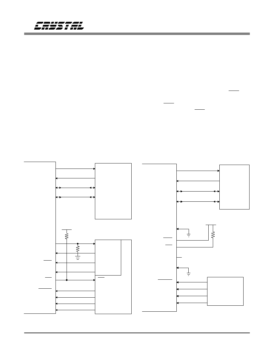
Applications of SM4
Figure 15 illustrates one method of using serial
mode 4 wherein a DSP controls the audio serial
port and a microcontroller controls the control
port. Each controller is run independently and
the micro updates the control information only
when needed, or when an interrupt from the
CS4216 occurs.
Figure 16 illustrates the minimum interface to
the CS4216. In this application, the DSP sends
and receives stereo DAC and ADC information.
The CS4216 is configured for 32 bits per frame,
Master sub-mode. The control data resets to all
zeros, which configures the CS4216 as a simple
stereo codec: no gain, no attenuation, line inputs
#1, and not muted.
Figure 17 illustrates how to use all the CS4216
features with a low cost DSP that cannot support
the interrupt rate of SM3. Using SM4 (32 bits
16
17
32
MF4:CCS
MF3:CCLK
1
8
9
24
25
1 0 3
0
Err
Version
MS
K
DO
1
MF2:CDIN
MF1:CDOUT
0
0 0 0 1
Left
A/D Gain
3
0
Right
A/D Gain
3
0
M
In
Sel.
Left
D/A Att.
4
0
Right
D/A Att.
4
0
AD
V
LC
L
RCL
1 0
Err
AD
V
LC
L
RCL
DI
1
0 0 0 0 0 0 0 0
DI
1
0
Figure 14. SM4 - Control Serial Port
SCLK to CLKIN Ratio
Fs (kHz)
Fs (kHz)
BPF
BPF
BPF
with CLKIN with CLKIN
128
64
32
12.288 MHz 11.2896 MHz
2
4
8
48.00
44.10
3
6
12
32.00
29.40
4
8
16
24.00
22.05
5
10
20
19.20
17.64
6
12
24
16.00
14.70
8
16
32
12.00
11.025
10
20
40
9.60
8.82
12
24
48
8.00
7.35
Table 9. SM4-Slave, Fs Select.
CS4216
22
DS83F2
per frame, Master sub-mode) reduces the DSP
interrupts in half since the control data is split
from the audio data. This circuit is comprised of
three independent sections which may individu-
ally be eliminated if not needed.
To load control data into the codec, three
HC597's are utilized. These are both latches that
store the DSP-sent control data, and shift regis-
ters that shift the data into the codec. The codec
uses an inverted SSYNC signal to copy the
latches to the shift registers every frame. In this
diagram the DSP is assumed to have a data bus
bandwidth of at least 24 bits. If the DSP has less
than 24_bits, the three HC597s must be split into
two addresses. Since the HC597 internal latches
are copied to the shift registers, the latches con-
tinually hold the DSP-sent data; therefore, the
DSP only needs to write data to the latches when
a change is desired.
The second section is comprised of an HC595
shift register and latch that is clocked by an in-
verted SCLK The data shifted into the HC595 is
transferred to the HC595's latch by the SSYNC
signal. This HC595 captures the 8 bits prior to
the SSYNC signal (which is also MF4:CCS) go-
ing high. As shown in Figure 14, and assuming
the MF4:CCS (SSYNC) signal rises at bit 32,
the 8-bits prior to MF4:CCS rising are a copy of
all the important status bits. This allows one shift
register to capture all the important information.
The interrupt pin cannot reliably be used in this
configuration since the interrupt pin is cleared by
reading the control port which occurs asynchro-
Micro-
Controller
Serial
Port
General
Purpose
Port
Pins
IRQ
DSP
SDOUT
SDIN
SSYNC
SCLK
CS4216
MF1:CDOUT
MF2:CDIN
MF4:CCS
MF3:CCLK
RESET
MF8:F3
MF7:F2
MF6:F1
MF5:INT
SM4
VD+
43
42
1
44
40
39
36
35
38
2
34
31
30
Figure 15. SM4 - Microcontroller Interface
DSP
SDOUT
SDIN
SSYNC
SCLK
CS4216
MF1:CDOUT
MF2:CDIN
MF4:CCS
MF3:CCLK
MF5:INT
SM4
VD+
RESET
MF8:F3
MF7:F2
MF6:F1
Hard Wired or
DIP Switch
selectable
32 BPF
43
42
1
44
35
36
38
40
39
2
34
31
30
Figure 16. SM4 - Minimum DSP Interface
CS4216
DS83F2
23
DSP
SDOUT
SDIN
SSYNC
SCLK
CS4216
MF1:CDOUT
MF2:CDIN
MF4:CCS
MF3:CCLK
RESET
MF8:F3
MF7:F2
MF6:F1
HC574
HC595
SCLK
LCLK
AIN
A
B
C
D
E
F
G
H
0
ADV
DI1
RCL
LCL
ERR0
ERR1
0
HC597
HC597
HC597
DOUT
LOAD
DIN
CS_FS
OE
CS_STATUS
CS_CONTROL
24+ bit DSP Data Bus
MF5:INT
SM4
32 BPF
VD+
43
42
1
44
35
36
38
39
40
2
34
31
30
Figure 17. SM4 - Enhanced DSP Interface
CS4216
24
DS83F2

nously (every audio frame) with respect to the
interrupt occurrence.
The third section is only needed if sample fre-
quencies need to be changed. This section is
comprised of an HC574 octal latch that can be
replaced by general purpose port pins if avail-
able. This section controls the sample frequency
selection bits: MF6:F1, MF7:F2, MF8:F3 and
the RESET pin. The codec must be reset when
changing sample frequencies.
Power Supply and Grounding
The CS4216, along with associated analog cir-
cuitry, should be positioned in an isolated section
of the circuit board, and have its own, separate,
ground plane. On the CS4216, the analog and
digital grounds are internally connected; there-
fore, the AGND and DGND pins must be
externally connected with no impedance between
them. The best solution is to place the entire
chip on a solid ground plane as shown in Fig-
ure 18. Preferably, it should also have its own
power plane. The +5V supply must be connected
to the CS4216 via a ferrite bead, positioned
closer than 1" to the device. The VA supply can
be derived from VD, as shown in Figure 1. Al-
ternatively, a separate +5V analog supply may be
used for VA, in which case, the 2.0
resistor
between VA and VD should be removed. A sin-
gle connection between the CS4216 ground
(analog ground) and the board digital ground
should be positioned as shown in Figure 18.
Figure 19 illustrates the optimum ground and de-
coupling layout for the CS4216 assuming a
surface-mount socket and leaded decoupling ca-
pacitors. Surface-mount sockets are useful since
the pad locations are identical to the chip pads;
therefore, assuming space for the socket is left
on the board, the socket can be optional for pro-
duction. Figure 19 depicts the top layer,
containing signal traces, and assumes the bottom
or inter-layer contains a fairly solid ground
plane. The important points are that there is solid
ground plane under the codec on the same layer
as the codec and it connects all ground pins with
thick traces providing the absolute lowest imped-
ance between ground pins. The decoupling
capacitors are placed as close as possible to the
device which, in this case, is the socket bound-
ary. The lowest value capacitor is placed closest
to the codec. Vias are placed near the AGND and
DGND pins, under the IC, and should attach to
the solid ground plane on another layer. The
negative side of the decoupling capacitors should
also attach to the same solid ground plane.
Traces and vias bringing power to the codec
should be large, which minimizes the impedance.
Although not shown in the figures, the trace lay-
ers (top layer in the figures) should have ground
plane fill in-between the traces to minimize cou-
pling into the analog section. See the CDB4216
evaluation board as an example.
If using all surface-mount components, the de-
coupling capacitors should be placed on the
same layer as the codec and in the positions
shown in Figure 20. The vias shown are assumed
to attach to the appropriate power and ground
layers. Traces and vias bringing power to the
codec should be as large as possible to minimize
the impedance.
If using a through-hole socket, effort should be
made to find a socket with minimum height,
CS4216
DS83F2
25

which will minimize the socket impedance.
When using a through hole socket, the vias un-
der the codec in Figure 19 are not needed since
the pins serve the same function.
ADC and DAC Filter Response Plots
Figures 21 - 26 shows the overall frequency re-
sponse, passband ripple and transition band for
the CS4216 ADCs and DACs. Figure 27 shows
the DACs' deviation from linear phase.
Fs is defined as the selected sample frequency
and is also the SSYNC frequency. Since the
sample frequency is programmable, the filters
will adjust to the selected sample frequency.
Digital
Ground
Plane
Note that the CS4216
is oriented with its
digital pins towards the
digital end of the board.
CPU & Digital
Logic
Codec
digital
signals
Codec
analog
signals &
Components
> 1/8"
CS4216
+5V
Ferrite
Bead
Ground
Connection
Analog
Ground
Plane
Figure 18. CS4216 Board Layout Guideline
CS4216
26
DS83F2

1
1.0 uF
0.1 uF
10 uF
+
1.0 uF
0.1 uF
0.1 uF
+
+
Analog
Supply
Digital
Supply
Figure 19. CS4216 Decoupling Layout Guideline
1
1.0 uF
0.1 uF
10 uF
+
1.0 uF
0.1 uF
0.1 uF
+
+
Analog
Supply
Digital
Supply
Figure 20. CS4216 Surface Mount Decoupling Layout
CS4216
DS83F2
27
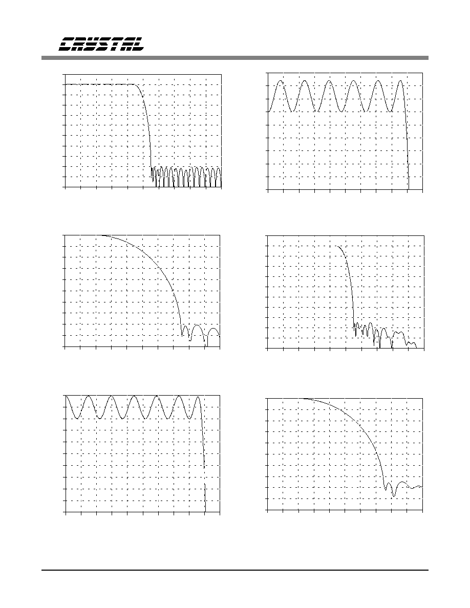
0.0
0.1
0.2
0.3
0.4
0.5
0.6
0.7
0.8
0.9
1.0
Input Frequency (Fs)
-100
-90
-80
-70
-60
-50
-40
-30
-20
-10
0
10
Magnitude (dB)
Figure 21. CS4216 ADC Frequency Response
0.00 0.05 0.10 0.15 0.20 0.25 0.30 0.35 0.40 0.45 0.50
Input Frequency (Fs)
-1.2
-1.0
-0.8
-0.6
-0.4
-0.2
-0.0
0.2
0.4
0.6
Magnitude (dB)
Figure 22. CS4216ADC Passband Ripple
0.40 0.42 0.44 0.46 0.48 0.50 0.52 0.54 0.56 0.58 0.60
Input Frequency (Fs)
-100
-90
-80
-70
-60
-50
-40
-30
-20
-10
0
Magnitude (dB)
Figure 23. CS4216 ADC Transition Band
0.0
0.1
0.2
0.3
0.4
0.5
0.6
0.7
0.8
0.9
1.0
Input Frequency (Fs)
-100
-90
-80
-70
-60
-50
-40
-30
-20
-10
0
10
Magnitude (dB)
Figure 24. CS4216 DAC Frequency Response
0.00 0.05 0.10 0.15 0.20 0.25 0.30 0.35 0.40 0.45 0.50
Input Frequency (Fs)
-0.8
-0.7
-0.6
-0.5
-0.4
-0.3
-0.2
-0.1
-0.0
0.1
0.2
Magnitude (dB)
Figure 25. CS4216 DAC Passband Ripple
-100
-90
-80
-70
-60
-50
-40
-30
-20
-10
0
Magnitude (dB)
0.40 0.42 0.44 0.46 0.48 0.50 0.52 0.54 0.56 0.58 0.60
Input Frequency (Fs)
Figure 26. CS4216 DAC Transition Band
CS4216
28
DS83F2

0.00 0.05 0.10 0.15 0.20 0.25 0.30 0.35 0.40 0.45 0.50
Input Frequency (Fs)
-2.5
-2.0
-1.5
-1.0
-0.5
0.0
0.5
1.0
1.5
2.0
2.5
Phase (degrees)
Figure 27. CS4216 DAC Deviation from Linear Phase
CS4216
DS83F2
29
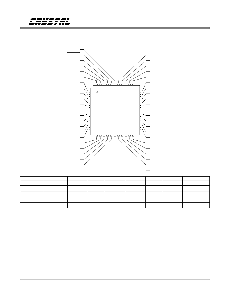
PIN DESCRIPTIONS
40
42
34
36
38
6
2
4
8
10
1
3
5
7
9
11
23
25
27
29
31
33
28
24
26
30
32
44
12
14
16
18
20
22
SM
MF1
MF2
MF3
MF4
MF5
MF6
MF7
MF8
1
DO4
DO3
DI3
DI4
DO2
DI2
SFS1
SFS2
2
DO4
DO3
DI3
DI4
DO2
DI2
SFS1
SFS2
3
F1
F2
F3
MA
DO2
DI2
SFS1
SFS2
4-SL
CDOUT
CDIN
CCLK
CCS
INT
F1
SFS1
SFS2
4-MA
CDOUT
CDIN
CCLK
CCS
INT
F1
F2
F3
SSYNC
RESET
SCLK
CLKIN
SDOUT
VD
SDIN
DGND
SMODE3
NC
MF1:DO4/F1/CDOUT
NC
MF2:DO3/F2/CDIN
NC
MF5:DO2/INT
NC
DO1
NC
MF4:DI4/MA/CCS
NC
MF3:DI3/F3/CCLK
NC
MF6:DI2/F1
PDN
DI1
NC
SMODE2
ROUT
MF7:SFS1/F2
LOUT
MF8:SFS2/F3
NC
SMODE1
NC
LIN2
NC
LIN1
REFBUF
RIN2
REFBYP
RIN1
REFGND
VA
AGND
CS4216
44-PIN
TQFP
(Q)
Top View
CS4216
30
DS83F2
Power Supply
VD - Digital +5V Supply, PIN 4(L), 42(Q).
+5V digital supply.
VA - Analog +5V Supply, PIN 24(L), 18(Q).
+5V analog supply.
DGND - Digital Ground, PIN 5(L), 43(Q).
Digital ground. Must be connected to AGND with zero impedance.
CS4216
44-PIN
PLCC
(L)
Top View
SM
MF1
MF2
MF3
MF4
MF5
MF6
MF7
MF8
1
DO4
DO3
DI3
DI4
DO2
DI2
SFS1
SFS2
2
DO4
DO3
DI3
DI4
DO2
DI2
SFS1
SFS2
3
F1
F2
F3
MA
DO2
DI2
SFS1
SFS2
4-SL
CDOUT
CDIN
CCLK
CCS
INT
F1
SFS1
SFS2
4-MA
CDOUT
CDIN
CCLK
CCS
INT
F1
F2
F3
SSYNC
RESET
SCLK
CLKIN
SDOUT
VD
SDIN
DGND
SMODE3
NC
MF1:DO4/F1/CDOUT
NC
MF2:DO3/F2/CDIN
NC
MF5:DO2/INT
NC
DO1
NC
MF4:DI4/MA/CCS
NC
MF3:DI3/F3/CCLK
NC
MF6:DI2/F1
PDN
DI1
NC
SMODE2
ROUT
MF7:SFS1/F2
LOUT
MF8:SFS2/F3
NC
SMODE1
NC
LIN2
NC
LIN1
REFBUF
RIN2
REFBYP
RIN1
REFGND
VA
AGND
CS4216
44-PIN
PLCC
(L)
Top View
18
20
22
24
26
28
1
2
4
6
40
42
44
12
8
10
14
16
7
9
11
13
15
17
29
31
33
35
37
39
34
30
32
36
38
CS4216
DS83F2
31

AGND - Analog Ground, PIN 23(L), 17(Q).
Analog ground. Must be connected to DGND with zero impedance.
Analog Inputs
RIN1 - Right Input #1, PIN 25(L), 19(Q).
Right analog input #1. Full scale input, with no gain, is 1 Vrms, centered at REFBUF.
RIN2 - Right Input #2, PIN 26(L), 20(Q).
Right analog input #2. Full scale input, with no gain, is 1 Vrms, centered at REFBUF.
LIN1 - Left Input #1, PIN 27(L), 21(Q).
Left analog input #1. Full scale input, with no gain, is 1 Vrms, centered at REFBUF.
LIN2 - Left Input #2, PIN 28(L), 22(Q).
Left analog input #2. Full scale input, with no gain, is 1 Vrms, centered at REFBUF.
Analog Outputs
ROUT - Right Channel Output, PIN 15(L), 9(Q).
Right channel analog output. Maximum signal is 1 Vrms centered at REFBUF.
LOUT - Left Channel Output, PIN 16(L), 10(Q).
Left channel analog output. Maximum signal is 1 Vrms centered at REFBUF.
REFBYP - Analog Reference Decoupling, PIN 21(L), 15(Q).
A 10
µ
F and 0.1
µ
F capacitor must be attached between REFBYP and REFGND.
REFGND - Analog Reference Ground Connection, PIN 22(L), 16(Q).
Connect to AGND.
REFBUF - Buffered Reference Out, PIN 20(L), 14(Q).
A nominal +2.2 V output for setting the bias level for external analog circuits.
Serial Digital Audio Interface Signals
SDIN - Serial Port Data In, PIN 42(L), 36(Q).
Digital audio data to the DACs and level control information is received by the CS4216 via
SDIN.
SDOUT - Serial Port Data Out, PIN 43(L), 37(Q).
Digital audio data from the ADCs and status information is output from the CS4216 via
SDOUT.
SCLK - Serial Port Bit Clock, PIN 44(L), 38(Q).
SCLK controls the digital audio data on SDOUT and latches the data on SDIN.
CS4216
32
DS83F2

SSYNC - Serial Port Sync Signal, PIN 1(L), 39(Q).
Indicates the start of a digital audio frame in SM3 and SM4, and also the start of a word in
SM1 & SM2.
SMODE1 - Serial Mode Select, PIN 29(L), 23(Q).
One of three pins that select the serial mode and function of the multifunction pins.
SMODE2 - Serial Mode Select, PIN 32(L), 26(Q).
One of three pins that select the serial mode and function of the multifunction pins.
SMODE3 - Serial Mode Select, PIN 41(L), 35(Q).
One of three pins that select the serial mode and function of the multifunction pins. This pin
has an internal pull-down making this revision backwards compatible with a previous version
(Revision A or Version3-Version0 bits = 0000).
Multifunction Digital Pins
MF1:DO4 - Parallel Digital Bit Output #4 in SM1/SM2, PIN 40(L), 34(Q).
In serial modes 1 and 2 this pin reflects the value of the DO4 bit in the sub-frame.
MF1:F1 - Format bit 1 in SM3, PIN 40(L), 34(Q).
In serial mode 3 this pin is a format bit and is used as one of three sample frequency select pins
when in master mode, or as one of two bits-per-frame select pins when in slave mode.
MF1:CDOUT - Control Data Output in SM4, PIN 40(L), 34(Q).
In serial mode 4 this pin is the data output for the control port which contains status
information.
MF2:DO3 - Parallel Digital Bit Output #3 in SM1/SM2, PIN 39(L), 33(Q).
In serial modes 1 and 2 this pin reflects the value of the DO3 bit in the sub-frame.
MF2:F2 - Format bit 2 in SM3, PIN 39(L), 33(Q).
In serial mode 3 this pin is a format bit and is used as one of three sample frequency select pins
when in master mode, or as one of two bits-per-frame select pins when in slave mode.
MF2:CDIN - Control Data Input in SM4, PIN 39(L), 33(Q).
In serial mode 4 this pin is the control port data input which contains data such as gain and
attenuation settings as well as input select, mute, and digital output bits.
MF3:DI3 - Parallel Digital Bit Input #3 in SM1/SM2/SM3 (Slave), PIN 35(L), 29(Q).
In serial modes 1 and 2 this pin value is reflected in the DI3 bit in the sub-frame.
MF3:F3 - Format bit 3 in SM3 (Master), PIN 35(L), 29(Q).
In serial mode 3 this pin is a format bit and is used as one of three sample frequency select pins
when in master mode. In slave mode, the pin reverts to being a general purpose input.
MF3:CCLK - Control Data Clock in SM4, PIN 35(L), 29(Q).
In serial mode 4 this pin is the control port serial bit clock which latches data from CDIN on
the falling edge, and outputs data onto CDOUT on the rising edge.
CS4216
DS83F2
33

MF4:DI4 - Parallel Digital Bit Input #4 in SM1/SM2, PIN 36(L), 30(Q).
In serial modes 1 and 2 this pin value is reflected in the DI4 bit in the sub-frame.
MF4:MA - Master Sub-Mode in SM3, PIN 36(L), 30(Q).
In serial mode 3 this pin selects either master or slave mode. When MF4:MA = 1, the codec is
in master mode and outputs SSYNC and SCLK. When MF4:MA = 0, the codec is in slave
mode and receives SSYNC and SCLK from an external source that must be frequency locked to
CLKIN.
MF4:CCS - Control Data Chip Select in SM4, PIN 36(L), 30(Q).
In serial mode 4 this pin is the control port chip select signal. When low, the control port data is
clocked in CDIN and status data is output on CDOUT. When CCS goes high, control data is
latched internally. This data remains active until new data is clocked in. The control port may
also be asynchronous to the audio data port.
MF5:DO2 - Parallel Digital Bit Output #2 in SM1/SM2/SM3, PIN 38(L), 32(Q).
In serial modes 1, 2, and 3 this pin reflects the value of the DO2 bit in the sub-frame.
MF5:INT - Interrupt in SM4, PIN 38(L), 32(Q).
In serial mode 4 this pin is an active low interrupt signal that is maskable using the MSK bit in
the control port serial data stream. INT is an open-collector output and requires and external
pull-up resistor. Assuming the mask bit is not set, and interrupt is triggered by a change in ADV
or DI1, or a rising edge on LCL or RCL, or a exiting an SCLK out of range condition
(Error = 3)
MF6:DI2 - Parallel Digital Bit Input #2 in SM1/SM2/SM3, PIN 34(L), 28(Q).
In serial modes 1, 2, and 3 this pin value is reflected in the DI2 bit of the sub-frame.
MF6:F1 - Format Bit 1 in SM4, PIN 34(L), 28(Q).
In serial mode 4 this pin is a format bit and is used as one of three sample frequency select pins
when in master mode. In slave mode, MF6:F1 helps determine the number of sub-frames within
a frame.
MF7:SFS1 - Sub-Frame Select 1 in SM1/SM2/SM3/SM4-SL, PIN 31(L), 25(Q).
In serial modes 1, 2, and 3, MF7:SFS1 helps select the sub-frame that this particular CS4216 is
allocated. In slave sub-mode of serial mode 4, this pin is one of two pins used as a sub-frame
select when MF6:F1 = 1 (128-bit frames). When MF6:F1 = 0, this pin is used to select the
frame sizes of 32 or 64 bits.
MF7:F2 - Format Bit 2 in SM4-MA, PIN 31(L), 25(Q).
In master sub-mode of serial mode 4, this pin is used as one of three sample frequency select
pins.
MF8:SFS2 - Sub-Frame Select 2 in SM1/SM2/SM3/SM4-SL, PIN 30(L), 24(Q).
In serial modes 1, 2, 3, and slave sub-mode of 4, MF8:SFS2 helps select the sub-frame that this
particular CS4216 is allocated.
MF8:F3 - Format Bit 3 in SM4-MA, PIN 30(L), 24(Q).
In master sub-mode of serial mode 4, this pin is a format bit and is one of three sample
frequency select pins.
CS4216
34
DS83F2

Miscellaneous
RESET - Reset Input, PIN 2.(L), 40(Q).
Resets the CS4216 into a known state, and must be initiated after power-up or power-down
mode. Releasing RESET caused the CS4216 to initiate a calibration sequence. RESET should
also be initiated when changing sample frequencies in any master sub-mode.
CLKIN - Master Clock, PIN 3(L), 41(Q).
C LKIN is the m ast er clock t h at operat es t h e int ernal logic. In serial mode 1,
CLKIN = 512
◊
hFs, where hFs is the highest sample frequency needed. Different sample
frequencies are obtained by changing the ratio of SCLK to CLKIN. In serial mode 2, CLKIN is
not used and must be tied low. In serial modes 3 and 4, CLKIN is 256
◊
hFs, where different
sample frequencies are obtained by either changing the ratio of SCLK to CLKIN in slave mode,
or changing the format pin values (F2-F0) in master mode.
PDN - Power Down, PIN 13(L), 7(Q).
This pin, when low, causes the CS4216 to go into a power down state. RESET should be held
low for 50 ms when exiting the power down state to allow time for the voltage reference to
settle.
DI1 - Parallel Digital Bit Input #1, PIN 33(L), 27(Q).
This pin value is reflected in the DI1 bit in the sub-frame.
DO1 - Parallel Digital Bit Output #1, PIN 37(L), 31(Q).
This pin reflects the value of the DO1 bit in the sub-frame.
NC - No Connection, PINS 6, 7, 8, 9, 10, 11, 12, 14, 17, 18, 19(L)
PINS 44, 1, 2, 3, 4, 5, 6, 8, 11, 12, 13(Q).
These pins should be left floating with no trace attached to allow backwards compatibility with
future revisions. They should not be used as a convenient path for signal traces.
CS4216
DS83F2
35

PARAMETER DEFINITIONS
Resolution
The number of bits in the input words to the DACs, and in the output words from the ADCs.
Differential Nonlinearity
The worst case deviation from the ideal codewidth. Units in LSB.
Total Dynamic Range
TDR is the ratio of the rms value of a full scale signal to the lowest obtainable noise floor. It is
measured by comparing a full scale signal to the lowest noise floor possible in the codec (i.e.
attenuation bits for the DACs at full attenuation). Units in dB.
Instantaneous Dynamic Range
IDR is the ratio of a full-scale rms signal to the rms noise available at any instant in time,
without changing the input gain or output attenuation settings. It is measured using S/(N+D)
with a 1 kHz, -60 dB input signal, with 60 dB added to compensate for the small input signal.
Use of a small input signal reduces the harmonic distortion components to insignificance when
compared to the noise. Units in dB.
Total Harmonic Distortion
THD is the ratio of the rms value of a signal's first five harmonic components to the rms value
of the signals fundamental component. THD is calculated using an input signal which is 3dB
below typical full-scale, and is referenced to typical full-scale.
Interchannel Isolation
The amount of 1 kHz signal present on the output of the grounded input channel, with 1 kHz
0 dB signal present on the other channel. Units in dB.
Interchannel Gain Mismatch
For the ADCs, the difference in input voltage that generates the full scale code for each
channel. For the DACs, the difference in output voltages for each channel with a full scale
digital input. Units in dB.
Frequency Response
Worst case variation in output signal level versus frequency over the passband. Tested over the
frequency band of 10 Hz to 20 kHz, with the sample frequency of 48 kHz. Units in dB.
Step Size
Typical delta between two adjacent gain or attenuation values. Units in dB.
Absolute Gain/Attenuation Step Error
The deviation of a gain or attenuation step from a straight line passing through the
no-gain/attenuation value and the full-gain/attenuation value (i.e. end points). Units in dB.
Offset Error
For the ADCs, the deviation of the output code from the mid-scale with the selected input at
REFBUF. For the DACs, the deviation of the output from REFBUF with mid-scale input code.
Units in LSB's for the ADCs and volts for the DACs.
CS4216
36
DS83F2

Out of Band Energy
The ratio of the rms sum of the energy from 0.46
◊
Fs to 2.1
◊
Fs compared to the rms full-scale
signal value. Tested with 48 kHz Fs giving a out-of-band energy range of 22 kHz to 100 kHz.
CS4216
DS83F2
37

APPENDIX A
This data sheet describes version 1 of the CS4216. Therefore, this appendix is included to describe the
differences between version 0 and version 1. This information is only useful for users that still have
version 0 since version 1 devices will supplant the earlier version. The version number is contained in
the serial data line, bits 29 - 32 on SDOUT in SM1-SM3 and, bits 17 - 20 on CDOUT in SM4. The
version number can also be identified by the revision letter stamped on the top of the actual chip. The
revision letter immediately precedes the data code on the second line of the package marking (See
General Information section of the Crystal Data Book). Version 0 corresponds to chip revision A, and
version 1 corresponds to chip revisions B, and C. The functionally and performance of revisions B
and C are identical. Likewise, future chip revisions (i.e. D, E, F, . . .) may still be version 1 since the
version number only changes if there is a software change to the part.
Functional Differences Between Version 0 (Rev. A) and Version 1 (Revs. B, C)
1. In version 0, serial mode 4 (SM4) does not exist; the SMODE3 pin is a no connect. In version 1 the
SMODE3 pin contains an internal pull-down resistor making this version backwards compatible with
version 0 sockets.
2. SSYNC on version 0 must be ONLY one SCLK period high in SM3 or 2 SCLK periods high in
SM1 and SM2 to indicate the start of a frame. Also, on version 0 in SM1 or SM2, SSYNC must be
EXACTLY one SCLK period high, at the beginning of each word. In version 1, SSYNC can be high
for an arbitrary number of SCLKs beyond the one in SM3 or two in SM1 and SM2. Also in SM1 and
SM2, the one-SCLK-wide SSYNCs at each word are not needed. In version 1, SM3 and SM4, the
codec only looks for a low-to-high edge of SSYNC to start a frame; in SM1 and SM2 a low-to-high
edge of SSYNC, being high for two SCLK periods, starts a frame.
CS4216
38
DS83F2

Features
∑
∑
Easy DSP Hook-Up
∑
∑
Analog-in To Analog-out Loopback
Mode
∑
∑
Correct Grounding and Layout
∑
∑
Microphone Pre-amplifier
∑
∑
Line Input Buffer
∑
∑
Digital and Analog Patch Areas
General Description
The CDB4216 and CDB4218 evaluation boards allow
easy evaluation of the CS4216 and CS4218 audio mul-
timedia codecs. Analog inputs provided include two
BNC line inputs for LIN1 and RIN1, and two
1
/
4
" micro-
phone jacks on the LIN2 and RIN2 lines. Analog
outputs are available on two BNCs.
Digital interfacing is facilitated using one to three of the
buffered ribbon cable headers. All four serial modes of
the CS4216 and all three modes of the CS4218 are
supported using a simple DIP switch which is decoded
to select the proper mode and sub-mode.
ORDERING INFORMATION: CDB4216 or CDB4218
JUN '93
CS83DB4
39
Crystal Semiconductor Corporation
P.O. Box 17847, Austin, TX 78760
(512) 445 7222 Fax: (512) 445 7581
CS4216 Evaluation Board
Semiconductor Corporation
CDB4216
CS4216
VA
Digital
I/O
Buffers
&
MUX
Digital Patch
Area
AGND
VD
DGND
CLKIN
Audio
Port
Control
Port
Line Inputs
Microphone
Jacks
Line Outputs
A = 14 dB
A = - 6 dB
(+5V)
Analog Patch
Area
LIN2
RIN2
LIN1
RIN1
LOUT
ROUT
OSC
Digital
I/O Port
Configuration
Switch
(+5V)
Copyright
©
Crystal Semiconductor Corporation 1993
(All Rights Reserved)

GENERAL DESCRIPTION
The CDB4216/8 was designed to provide an
easy platform for evaluating the performance of
the CS4216 and CS4218 Stereo Audio Codecs.
Since the evaluation board contains a proper lay-
out and is performance tested, the user can
concentrate on engineering the rest of the system
thereby reducing the development time. The lay-
out should also be used as a guideline for
obtaining the best possible performance from the
CS4216 or CS4218. Lastly, the board can be
used as a benchmark and debugging tool for user
developed PCBs.
The evaluation board supports all serial modes
and includes decode circuitry to ease the selec-
tion of the serial mode and sub-mode of interest.
All serial interfaces are buffered for easy connec-
tion to the serial port of a DSP or other serial
device. The board can also be placed in a loop
back mode where the digital data is looped back
allowing an analog in to analog out testing vehi-
cle without an external processor. A single +5V
supply is all that is needed to power the board.
Analog inputs consist of a pair of line input buff-
ers (LIN1, RIN1) designed to accept a maximum
audio signal of 2V
RMS
and BNC-to-phono
adapters are included to support various test con-
figurations. The second pair of inputs contain a
example microphone input buffer supported by
two
1
/
4
" mono jacks that are designed to accept
standard single-ended dynamic or condenser mi-
crophones.
The line outputs are supplied via BNC connec-
tors with two more BNC-to-phono adapters.
The film plots of the evaluation board are in-
cluded to provide an example of the optimum
layout, grounding, and decoupling arrangement
for the CS4216 or CS4218.
SELECTING A SERIAL MODE
The CS4216 supports four serial modes and
many sub-modes, and the CS4218 supports three
serial modes and sub-modes. Selecting the most
appropriate mode for a given application can be
time consuming. The CDB4216/8 contains a DIP
switch that simplifies this selection. Since the
CS4216/8 contains many multifunction pins, the
DIP switch lets the user select the configuration
and two PLDs decode the proper multifunction
pin values. Since these PLDs are only used to
simplify the configuration of the device, they
would not be needed in an end application which
would hard wire the configuration pins. Table 4
describes the multifunction pin values for a
given DIP switch setting. The PAL equations for
DIP switch decoding are given in Figures 8 and
9.
All references to SM1 and SM2 apply only to
the CS4216. All references to SM3-MM, SM3-
MS, and I
2
S apply only to the CS4218.
Serial Port Format
Table 1 lists the DIP switches used to select the
serial mode. SPF2 and SPF1 select one the four
serial modes of the CS4216 or one of three serial
modes for the CS4218. MA selects master
(MA = 1) or slave and is only useful in serial
modes 3 and 4. The majority of users select
SPF2
SPF1
MA
Serial Mode
0
0
x
SM1
Slave
0
1
x
SM2
Slave
1
0
0
SM3
Slave
1
0
1
SM3
Master
1
1
0
SM4
Slave
1
1
1
SM4
Master
Table 1. DIP Switch, Serial Modes
CDB4216
40
DS83DB4
either serial mode 3, SM3, or serial mode 4,
SM4. Serial modes 1 and 2, SM1 and SM2, are
primarily designed for ASICs and are less flex-
ible. SM1 and SM2 are not available on the
CS4218. The CS4218 has additional SM3 sub-
modes: Multiplier Master (SM3-MM) and
Multiplier Slave (SM3-MS). These sub-modes
are identical to the SM3 Master and Slave sub-
modes except that the master clock, CLKIN,
must be 16xFs
max
instead of 256xFs
max
. The
CS4218 also provides a master I
2
S mode. In
master sub-modes, the CS4216/8 output SSYNC
and SCLK. In slave sub-modes, SSYNC and
SCLK must be externally generated and must be
synchronous to CLKIN.
Bits per Frame Selection
The next decision is selecting the number of bits
per frame which defines how many codecs can
sit on the same serial bus. Each codec occupies a
sub-frame and 1 to 4 sub-frames make up a
frame. A sub-frame is 64 bits in SM1, SM2, and
SM3; and 32 bits in SM4. Table 2 lists the possi-
ble selections. If the evaluation board serial port
is shared with other devices, SDOUTUB must be
used instead of SDOUT since SDOUTUB,
driven directly from the chip, must only drive
the time slot assigned to it. See the Audio Port
Header section for more information.
Time Slot Selection
If the number of bits per frame selected allows
for more than one codec sub-frame, then the ac-
tual time slot or sub-frame used by the eval
board must be selected. This is done with the
TS2 and TS1 DIP switches. If the number of bits
per frame allows only one codec on the serial
bus, then TS2 and TS1 are ignored. Table 3 list
the decoding for TS2 and TS1. Time slot 1 is the
first sub-frame after SSYNC goes high, time
slot 2 is the next sub-frame, and so on.
Sample Frequency Selection - Master Mode
The last decision is selecting the sample fre-
quency in master sub-mode. If configured for
slave sub-mode, the sample frequency is the ratio
o f S C L K t o C LK IN as d es c ri b ed i n t h e
CS4216/8 Data Sheets. In master modes, three
pins are used to select the sample frequency di-
vide. The DIP switches labeled DIV1, DIV2, and
DIV3 select the sample frequency and are
equivalent to F1, F2, and F3, respectively. The
actual F1-F3 pins on the CS4216/8 are different
between SM3 and SM4 as shown in Table 4 at
the end of the data sheets. Table 3 and Table 9 of
the CS4216 Data Sheet describe the sample fre-
quencies obtained using the on-board oscillator
of 11.2896 MHz. As an example, if all DIV
switches are off, the sample frequency is
44.1 kHz. With only DIV2 on, the sample fre-
quency is 22.05 kHz. To obtain a sample
frequency of 44.1 kHz using the CDB4218, all
DIV switches should be set to zero and a
705.6 kHz clock should be connected to the
BNC jack (J2). The shunt on J1 should be set to
EXT.
BPF
SM1
SM3 SM4
2
1
SM2
SL
MA
SL
MA
0
0
256
64
64
32
32
0
1
256
128
128
64
64
1
0
256
256
128
128
64
1
1
256
256*
128
128
64
* SCLK is master clock.
Table 2. DIP Switch, Bits per Frame
TS2
TS1
Available Sub-frames
4
2
1
0
0
1
1
1
0
1
2
2
1
1
0
3
2
1
1
1
4
2
1
Table 3. DIP Switch, Time Slots
CDB4216
DS83DB4
41

DIP SWITCH MAPPING TO MULTI-FUNC-
TION PINS
The two PALs on the evaluation board decode
the DIP switches to configure the codec into a
particular mode. These PALs are not necessary
in a design since only one mode is usually used
and can be hard wired. Figure 9 and Figure 10
list the PAL equations used for decoding.
Table 4 shows the CS4216/8 multi-function pin
settings for each possible DIP switch configura-
tion. Refer to the CS4216/8 data sheets to
determine pin settings for sample frequencies.
Once a suitable mode has been chosen using the
evaluation board, this table will show the hard
wire configuration for each multi-function pin.
Example Mode Settings
Following are two examples of how to set a se-
rial mode with the DIP switches and then
determine the multi-function pin settings for the
codec. These modes were chosen for illustration
only, not to suggest that they are better than
other modes.
A commonly used mode is SM3 Master (SM3-M
on the CS4218), 64 BPF, 44.1kHz sampling rate,
and bit-long SSYNC. To configure the codec in
this mode, set SPF2=MA=1 and all other DIP
switches to zero. From Table 4, the SMODE3,
SMODE2, and SMODE1 pins are set to 010, re-
spectively. The DIV1, DIV2, and DIV3 DIP
switches will set the sampling frequency by di-
rectly mapping to the MF1, MF2, and MF3 pins
as 000. The MA DIP switch sets the MF4 pin
high for master mode. multi-function pins MF5
and MF6 become the general purpose I/O pins
DO2 and DI2, respectively. In this particular
mode, MF7 determines the high time for the
SSYNC signal. The MF7 pin is set low by the
TS1 switch to generate the bit-long SSYNC. In
all other applicable cases, the TS1 switch is used
for time-slot configuration. 64 BPF is selected
by setting the MF8 pin low with the BPF1
switch.
SM4 is a powerful mode which reduces data
transfer bandwidth to facilitate easier use with
low cost DSPs. As an example, consider SM4,
Slave, 64 BPF, Time-slot 2, and a 22.05 kHz
s amp lin g r a te. Se t
SPF2=SPF1=DIV1=TS1=BPF1=1 and all other
DIP switches to zero. Table 4 shows that the
SMODE3, SMODE2, and SMODE1 pins will be
set to 110, respectively. The multi-function pins
MF1-4 will become the control port interface.
MF5 serves as the interrupt pin INT. BPF2 and
BPF1 will set the codec to 64 BPF by mapping
directly to the MF6 and MF7 pins as 01, respec-
tively. The second time-slot is chosen with TS1
DIP SWITCHES
SPF2 SPF1 MA
SMODE SMODE SMODE
MF1
MF2
MF3
MF4
MF5
MF6
3
2
1
MF7
MF8
CS4216 Multifunction Pins
DO4
0
0
x
0
0
0
DO3
DI3
DI4
DO2
DI2
TS1
TS2
DO4
0
1
x
0
0
1
DO3
DI3
DI4
DO2
DI2
TS1
TS2
BPF2
0
1
0
0
1
0
BPF1
DI3
MA=0
DO2
DI2
TS1
TS2
DIV1
0
1
1
0
1
0
DIV2
DIV3
MA=1
DO2
DI2
TS1
BPF1
CDOUT
1
1
0
1
1
0
CDIN
CCLK
CCS
INT
BPF2=0
BPF1
TS1
CDOUT
1
1
0
1
1
0
CDIN
CCLK
CCS
INT
BPF2=1
TS1
TS2
CDOUT
1
1
1
1
BPF>0
TS1
CDIN
CCLK
CCS
INT
DIV1
DIV2
DIV3
CDOUT
1
1
1
1
BPF=0
0
CDIN
CCLK
CCS
INT
DIV1
DIV2
DIV3
Table 4. CS4216 Pin Decode
CDB4216
42
DS83DB4

VA
VD
CS4216
U1
CLKIN
LIN2
RIN2
LIN1
RIN1
28
26
27
25
24
4
Ferrite Bead
VA
(+5V)
VD
(+5V)
R26
2
L1
VA
DGND
AGND
VD
47 uF
+
C29
D4
P6KE
D3
P6KE
47 uF
+
C7
0.1 uF
C28
1 uF
+
C3
0.1 uF
C5
0.1 uF
C30
1 uF
+
C4
0.1 uF
C6
REFBYP
21
10 uF
+
C36
0.1 uF
C35
REFBUF
20
16
1 uF
C32
+
C31
2200 pF
NPO
15
1 uF
C34
+
C33
2200 pF
NPO
47.5 k
R28
47.5 k
R30
LOUT
ROUT
See Figure 7, 8
Line Input
Buffer
See Figure 2
Microphone
Input Buffer
See Figure 3
604
R27
604
R29
AGND
REFGND
DGND
23
22
5
MF4
MF3
MF6
SMODE3
SMODE2
SMODE1
MF7
MF8
3
32
29
31
30
RESET
41
2
36
35
34
See Figure 5
See Figure 5
See Figure 6
LOUT
ROUT
Figure 1. CS4216 and Power Supplies
CDB4216
DS83DB4
43

setting the MF8 pin high. Since the part is in
slave mode, the sampling rate must be set by the
ratio between CLKIN and SCLK. Assuming
that CLKIN has a frequency of 11.2896MHz,
this ratio must be eight to give a sampling rate of
22.05kHz (refer to the CS4216 data sheet). In
all slave modes, SSYNC and SCLK must be
synchronous to the master clock.
LOOPBACK MODE
The CDB4216/8 may be configured in a simple
loop back mode that only requires a power
source to operate. No controller of any type is
necessary. This mode allows a quick and simple
verification of codec operation by sampling the
LIN1 and RIN1 inputs, then looping the digital
data back to the LOUT and ROUT line outputs.
Set SPF2=SPF1=MA=1 and shunt SDOUT to
SDIN on stake header J15. This mode uses SM4
with all control settings set to zero, so no gain or
attenuation is available.
POWER SUPPLY CIRCUITRY
Figure 1 illustrates a portion of the CDB4216/8
schematic and includes the CS4216/8 along with
power supply decoupling and circuitry. The
evaluation board supports various power supply
arrangements. The factory configuration powers
the analog portion of the CS4216/8, along with
input buffers, from the VA binding post, which
needs a clean +5 Volts. The digital portions of
the CS4216/8 are factory configured to obtain
power through a 2
resistor from the VA supply.
The digital buffers and PLDs obtain power from
the VD binding post, which also needs +5 Volts.
Although binding posts exist for both digital and
analog grounds, only one needs to be connected
if a single supply is used for both VA and VD.
Note that the CS4216/8 is entirely on the analog
ground plane, close to the ground plane split as
required by the CS4216/8 Data Sheets. Also note
that the two ground planes are connected near
the two ground binding posts.
Space for a ferrite bead, L1, is provided so that
the board may be modified to power the codec
from the digital supply. Selection of L1 will de-
pend on the noise characteristics of the digital
supply used.
ANALOG INPUTS
The analog inputs consist of a pair of line level
inputs and a pair of
1
/
4
" mono jacks for two mi-
crophones. BNC-to-phono adapters are included
to allow testing of the line inputs using coax or
standard audio cables.
The line-level inputs are connected to the
CS4216/8's LIN1 and RIN1 pins. As shown in
Figure 2, the line-level inputs go through a buff-
er set to a gain of 0.5 which allows input signals
of up to 2 V
RMS
. When placed in serial mode 4
with loop back, the LIN1 and RIN1 inputs are
used for analog inputs.
The microphone inputs are connected to the
CS4216/8's LIN2 and RIN2 pins. The two mi-
crophone inputs are single-ended and are
designed to work with both condenser and dy-
namic microphones. The microphone input
buffer, shown in Figure 3, has a gain of 23 dB
thereby defining a full-scale input voltage to the
microphone jacks of 71 mV
RMS
. Another 22 dB
of programmable gain is available on the
CS4216/8 to amplify smaller microphone sig-
nals.
An analog patch area with analog power and
ground, included on the CDB4216/8, provides
space to develop other input buffer circuits.
Space for headers are included, J19 and J20, to
connect to the LIN2 and RIN2 inputs. To use
these headers, the microphone traces must be
cut.
ANALOG OUTPUTS
The CS4216/8 drives the line outputs into an R-
C filter and then to a pair of BNCs labeled
CDB4216
44
DS83DB4

150
0.47 uF
26
150
0.47 uF
28
RIN2
REFBUF
LIN2
20
CS4216
C19
R24
R25
C20
J19
LMIC
RMIC
J20
RIN2
1 uF
+
C21
2
3
VA
8
C16
1000 pF
NPO
+
R21
13 k
4
R18
47.5 k
LIN2
(Mono)
1 uF
+
C22
6
5
C15
1000 pF
R23
13 k
R19
47.5 k
NPO
C26
0.1 uF
1
7
U2
MC33178
+
R22
1k
R20
1 k
C23
10 uF
C24
10 uF
1 uF
+
C25
C37
0.1 uF
C17
0.01 uF
NPO
C18
0.01 uF
NPO
Figure 2. Microphone Input Buffer
REFBUF
LIN1
27
20
CS4216
0.01 uF
C13
NPO
20 k
+
_
10 k
56 pF
1 uF
C10
C8
R12
7
6
5
4
8
R14
LIN1
NPO
0.47 uF
C12
VA
C9
0.1 uF
RIN1
25
+
_
56 pF
C27
3
2
1
RIN1
(Mono)
20 k
R15
NPO
10 k
R13
1 uF
C11
U2
LT1013
0.01 uF
NPO
C14
150
R17
5 k
R11
150
R16
0.1 uF
C37
+
+
Figure 3. Line Input Buffer
CDB4216
DS83DB4
45

LOUT and ROUT. As with the line inputs, BNC-
to-phono adapters are provided for flexibility.
The line outputs can drive an impedance of
10 k
or more, which is the typical input imped-
ance of most audio gear.
AUDIO PORT HEADER
The CDB4216/8 is primarily designed to evalu-
ate the CS4216/8 in single chip mode, i.e. only
one codec on the serial bus. This is the factory
default state of the CDB4216/8.
The audio port header J15 provides all buffered
signals necessary to connect to the serial port of
a DSP or other controller (see Figure 4). SDOU-
TUB can provide an unbuffered version of
SDOUT which can be used when connecting
multiple codecs on the same bus. The default
configuration does not connect SDOUTUB
which may be connected to the SDOUT of the
CS4216/8 through J17 jumper.
The eval board supports both master and slave
sub-modes. In master sub-modes, SSYNC and
SCLK are output (and buffered) from the
CS4216/8. In slave sub-modes, SSYNC and
SCLK must be provided externally and must be
synchronous to the master clock CLKIN.
R32
20
R31
20
A0
A3
A2
A1
OEA
OEB
B3
B2
B1
B0
SSYNC
SCLK
R39
20
R44
10
R10
10
J17
U6
74HC243
CFSIN
R40
20
R41
20k
R49
100
9
13
8
4
J16
MF5
VD
PDN
J15
SDOUTUB
SDOUT
SDIN
SCLK
SSYNC
R46
47.5k
R42
28k
VD
D2
R38
806
SSYNC
SCLK
SDOUT
SDIN
DI1
MF1
MF2
MF5
PDN
DO1
CS4216
1
44
43
42
33
40
39
38
13
37
4
16
8
12
6
14
3
17
5
15
2
18
9
11
7
13
8
9
10
11
1
13
6
5
4
3
MF1b
DI1
DI4
DI3
DI2
J13
DI4
DI3
DI2
DI1
DO4
DO3
DO2
DO1
MF1a
MF2
1
19
U7
74HC541
OE1
OE2
J18
U
B
DO1
Q1
237k
R9
74HC541
U7
Figure 4. Serial Port Headers
CDB4216
46
DS83DB4

19
18
17
16
15
14
13
12
CFSIN
1
2
3
4
5
6
7
8
9
SMODE1
MF8
MF7
SMODE2
SMODE3
13
14
16
R49
100
1
2
3
4
5
6
7
8
9
10
11
1
R48
27k
DI4
DI3
DI2
DI1
2
3
4
5
6
R36
47k
R37
47k
R33
47k
VD
1
R35
47k
2
345
678
91
0
SW3
13
24
1
12
VD
1
23
456
MF1a
MF2
MF4
MF3
MF6
MF1b
R45
10k
VD
R53
27k
R54
27k
R47
27k
RESET
PDN
MF5
20
14
13
21
19
18
17
16
RESET
PDN
INT
CCS
CCLK
CDIN
CDOUT
U10
VD
1
2
3
4
5
6
7
8
9
R34
10k
J14
SWX
12
PALCE22V10Z
VD
24
C40
0.1uF
VD
20
C39
0.1uF
10
LB
SPF2
SPF1
MA
BPF2
BPF1
TS2
TS1
DIV3
DIV2
DIV1
SWX
U9
PALCE16V8Z
SWY
Fig
u
re
5
.
DI
P
Switc
h
De
co
de
+
Digit
a
l
He
ade
r
CDB4216
DS83DB4
47

CONTROL PORT HEADER
The Control Port Header J14 contains the control
port pins, available only in SM4, and the PDN
and RESET pins.
Serial mode 4, SM4, splits the serial data to the
codec into two separate serial ports, the audio
port and the control port. The control port pins
are available on this header. Since CDOUT is
buffered and always driven, it cannot be used on
a shared serial port. Although the INT pin on the
codec is open drain, the default factory configu-
ration for the eval board is an on-board pull-up
resistor and a buffer. Therefore, the INT header
pin cannot share an interrupt pin on a processor
since it is buffered and will always be driven. By
cutting a trace in the J18 jumper, the unbuffered
INT signal, labeled U, can be supplied to the
header. When using the control port, the LB
switch must be off or the control serial port will
be blocked.
PDN and RESET
PDN is buffered and controls the PDN pin on
the CS4216. PDN contains an on-board pull-up
resistor defining the default state as powered.
This pin only needs to be controlled when the
power down feature is used.
RESET is also buffered and controls the RESET
pin on the codec (see Figure 6). RESET has a
pull-up resistor on the board defining the default
state as not reset or active. This pin only needs
to be controlled when the reset feature on the
codec is needed. Since the codec requires a reset
at power up, a power-up reset circuit is included
on the board. A reset switch is also included to
allow resetting the device without having to re-
move the power supply. The power-up reset plus
switch are logically ORed with the RESET pin
on header J14.
DIGITAL I/O HEADER
The Digital I/O Header, J13 shown in Figure 4,
contains the four digital inputs, DI1-DI4, and the
four digital outputs, DO1-DO4. Note that all
digital I/O except DI1 and DO1 are multifunc-
tion pins and may not be available in a particular
mode. Since DO1 is always a digital output, an
LED is connected to DO1 providing a visual in-
dication that software is writing this bit correctly.
When the LED is on, DO1 is high.
In SM1 and SM2 all four digital inputs and out-
puts are available. In SM3 master sub-modes,
only the first two inputs and outputs are func-
tional. In SM3 slave sub-modes, three inputs and
two outputs are functional. In SM4 only DO1
and DI1 are functional. See the CS4216/8 Data
Sheet for more details.
CLOCKS
The CDB4216/8 provides an on-board default
clock oscillator of 11.2896 MHz (see Figure 7).
This allows all 44.1 kHz and derivative sample
frequencies in SM3 Master sub-mode, SM3
Slave sub-mode, SM4, and the I
2
S mode. The
CS4218 SM3-MM and SM3-MS modes require
a master clock of 16xFs
max
. If using SM1, a
master clock with a frequency that is 512xFs
max
must be supplied. SM2 uses SCLK as the master
clock ant it must be 256xFs
max
. A CLKIN BNC
allows the eval board to be driven from an exter-
VD
VD
RESET
U11
74HC132
R1
47.5k
R4
100
R3
100
SW1A
R2
47.5k
D1
1N4148
CS4216
RESET
2
+ C1
1 uF
8
9
10
11
12
13
Figure 6. Reset Circuit
CDB4216
48
DS83DB4
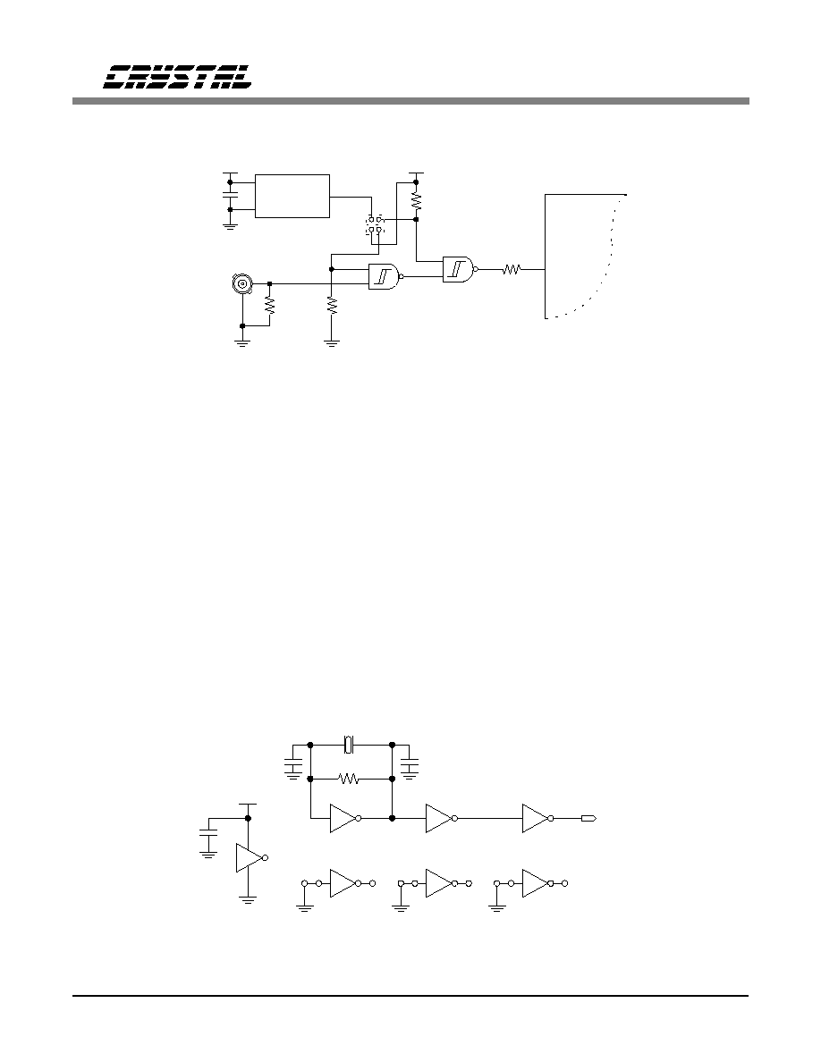
nal source. To select the CLKIN BNC, the J1
jumper must be placed in the EXT position.
When the J1 jumper is in the INT position, the
on-board oscillator is used as the master clock.
Both clock sources are buffered to guarantee a
clean signal and proper clock levels to the codec.
If sample frequencies other than the ones pro-
vided are needed, the oscillator can be replaced
with the proper frequency oscillator. The board
accepts crystals and provides the socket Y1 (refer
to Figure 8). When using a crystal, U8 must con-
tain an HCU04 unbuffered CMOS inverter. The
U8 socket is designed to accept either the
HCU04 or a crystal oscillator, and can alternate
between the two.
LAYOUT ISSUES
Figure 11 contains the silk screen, Figure 12
contains the component-side copper layer, and
Figure 13 contains the solder-side copper layer
of the CDB4216/8 evaluation board. These plots
are included to provide an example of how to
correctly layout a PCB for the codec.
Grounding and Power
U8
74HCUO4
Y1
R55
10M
C44
33 pF
C43
33 pF
CLKIN-J1
8
C2
0.1uF
VD
9
10
11
12
13
14
7
1
2
3
4
5
6
Figure 8. Optional Clock Circuit
U11B
74HC132
VD
4
5
3
1
2
3
CLKIN
6
CLKIN
U11A
CS4216
R8
10
J1
11.2896 MHz
Oscillator
Module
C2
0.1 uF
VD
EXT
INT
R5
47.5k
R7
5k
R6
47.5k
8
14
7
Figure 7. Default Clock Circuit
CDB4216
DS83DB4
49

Notice in Figure 12 and Figure 13 how the
ground plane split is positioned. The split is
next to the part - NOT UNDER IT. The AGND
and DGND pins are connected to the ground
plane fill inside the codec pad layout on the
component-side layer. This is recommended be-
cause AGND and DGND are connected on the
codec die and must have a zero impedance be-
tween them.
Notice how each ground connection has at least
four points in thermal relief. The main board
grounds at the terminal connections have eight
points in thermal relief. This helps minimize the
impedance to the main ground terminal from any
particular ground pin, reducing the chance of
noise coupling.
Another important design consideration is the
ground plane fill between traces on both layers,
which minimizes coupling of radiated energy.
Ground fill on the digital side of the board helps
reduce the amount of noisy digital energy radi-
ated to the sensitive analog side and to a host
system. Ground fill on the analog side helps re-
duce the amount of radiated digital energy that is
coupled into the analog circuitry. All ground
plane fills must be connected to their respective
grounds - floating ground fill is worse than no
fill.
All power and ground traces are as thick as the
surface mount pads they connect. Thick traces
minimize impedance, thereby reducing the
chance of noise coupling.
Decoupling
Notice how the decoupling capacitors are placed
as close as possible to the codec. The 0.1
µ
F ca-
pacitors are placed closer than the 10
µ
F or 1
µ
F
capacitors. This reduces lead inductance at high
frequencies and allows the smaller valued ca-
pacitors to attenuate unwanted signals more
effectively.
Sockets
The CDB4216/8 was designed to accommodate
either the 44-pin PLCC package or the 44-pin
TQFP package. Each evaluation board is
shipped with a PLCC codec loaded into a sur-
face mount socket. Notice how the socket pads
match the footprint of the PLCC package. Using
this socket in a design allows for testing with the
socket mounted, and the option to surface mount
the codec directly for cost reduction during
board production.
CDB4216
50
DS83DB4

;PALASM Design Description
;---------------------------------- Declaration Segment ------------
TITLE
CDB4216
PATTERN
4216S_B
REVISION
4.0B
AUTHOR
C. Sanchez, M. Jordan
COMPANY
Crystal Semiconductor
DATE
5/28/93
CHIP _4216s_b PALCE16V8
;---------------------------------- PIN Declarations ---------------
PIN
1
/SPF2
COMBINATORIAL ; INPUT
PIN
2
/SPF1
COMBINATORIAL ; INPUT
PIN
3
/MA
COMBINATORIAL ; INPUT
PIN
4
/BPF2
COMBINATORIAL ; INPUT
PIN
5
/BPF1
COMBINATORIAL ; INPUT
PIN
6
/TS2
COMBINATORIAL ; INPUT
PIN
7
/TS1
COMBINATORIAL ; INPUT
PIN
8
/DIV3
COMBINATORIAL ; INPUT
PIN
9
/DIV2
COMBINATORIAL ; INPUT
PIN
10
GND
PIN
11
NC
PIN
12
/CFSIN
COMBINATORIAL ; OUTPUT
PIN
13
NC
PIN
14
NC
PIN
15
SMODE3
COMBINATORIAL ; OUTPUT
PIN
16
SMODE2
COMBINATORIAL ; OUTPUT
PIN
17
MF7
COMBINATORIAL ; OUTPUT
PIN
18
MF8
COMBINATORIAL ; OUTPUT
PIN
19
SMODE1
COMBINATORIAL ; OUTPUT
PIN
20
VCC
;----------------------------------- Boolean Equation Segment ------
EQUATIONS
/CFSIN = SPF2 * MA
SMODE3 = SPF2 * SPF1
SMODE2 = SPF2 * /SPF1
+ SPF2 * SPF1 * /MA
+ SPF2 * SPF1 * MA * BPF1 * TS1
+ SPF2 * SPF1 * MA * BPF1 * TS2
+ SPF2 * SPF1 * MA * BPF2 * TS1
+ SPF2 * SPF1 * MA * BPF2 * TS2
SMODE1 = /SPF2 * SPF1
+ SPF2 * SPF1 * MA * BPF1
+ SPF2 * SPF1 * MA * BPF2
MF8 = /SPF2 * TS2
+ SPF2 * /SPF1 * MA * BPF2
+ SPF2 * /SPF1 * MA * BPF1
+ SPF2 * /SPF1 * /MA * BPF2 * TS2
+ SPF2 * SPF1 * /MA * /BPF2 * BPF1 * TS1
Figure 9. PALCE16V8H PAL Equations.
CDB4216
DS83DB4
51

+ SPF2 * SPF1 * /MA * /BPF2 * BPF1 * TS2
+ SPF2 * SPF1 * /MA * BPF2 * TS2
+ SPF2 * SPF1 * MA * DIV3
MF7 = /SPF2 * TS1
+ SPF2 * /SPF1 * /MA * /BPF2 * BPF1 * TS1
+ SPF2 * /SPF1 * /MA * /BPF2 * BPF1 * TS2
+ SPF2 * /SPF1 * /MA * BPF2 * TS1
+ SPF2 * /SPF1 * MA * TS1
+ SPF2 * SPF1 * /MA * /BPF2 * BPF1
+ SPF2 * SPF1 * /MA * BPF2 * TS1
+ SPF2 * SPF1 * MA * DIV2
Figure 9. Continued.
CDB4216
52
DS83DB4

;PALASM Design Description
;---------------------------------- Declaration Segment ------------
TITLE
CDB4216
PATTERN
4216L_B
REVISION
2.0B
AUTHOR
C. Sanchez
COMPANY
Crystal Semiconductor
DATE
4/27/93
CHIP _4216l_b PALCE22V10Z
;---------------------------------- PIN Declarations ---------------
PIN
1
/SPF2
COMBINATORIAL ; INPUT
PIN
2
/SPF1
COMBINATORIAL ; INPUT
PIN
3
/MA
COMBINATORIAL ; INPUT
PIN
4
/BPF2
COMBINATORIAL ; INPUT
PIN
5
/BPF1
COMBINATORIAL ; INPUT
PIN
6
/DIV3
COMBINATORIAL ; INPUT
PIN
7
/DIV2
COMBINATORIAL ; INPUT
PIN
8
/DIV1
COMBINATORIAL ; INPUT
PIN
9
DI4
COMBINATORIAL ; INPUT
PIN
10
DI3
COMBINATORIAL ; INPUT
PIN
11
DI2
COMBINATORIAL ; INPUT
PIN
12
GND
PIN
13
CDIN
COMBINATORIAL ; INPUT
PIN
14
CCLK
COMBINATORIAL ; INPUT
PIN
15
NC
PIN
16
MF6
COMBINATORIAL ; OUTPUT
PIN
17
MF3
COMBINATORIAL ; OUTPUT
PIN
18
MF4
COMBINATORIAL ; OUTPUT
PIN
19
MF2
COMBINATORIAL ; OUTPUT
PIN
20
/CCS
COMBINATORIAL ; INPUT
PIN
21
MF1
COMBINATORIAL ; OUTPUT
PIN
22
NC
PIN
23
NC
PIN
24
VCC
;----------------------------------- Boolean Equation Segment ------
EQUATIONS
MF1 = SPF2 * /SPF1 * MA * DIV1
+ SPF2 * /SPF1 * /MA * BPF2
MF1.TRST = SPF2 * /SPF1
MF2 = SPF2 * /SPF1 * MA * DIV2
+ SPF2 * /SPF1 * /MA * BPF1
+ SPF2 * SPF1 * CDIN
MF2.TRST = SPF2
MF3 = /SPF2 * DI3 + SPF2 * /SPF1 * /MA * DI3
+ SPF2 * /SPF1 * MA * DIV3
+ SPF2 * SPF1 * CCLK
MF4 = /SPF2 * DI4
Figure 10. PALCE22V10Z PAL Equations.
CDB4216
DS83DB4
53

+ SPF2 * /SPF1 * MA
+ SPF2 * SPF1 * /CCS
MF6 = /SPF2 * DI2 + /SPF1 * DI2
+ SPF2 * SPF1 * MA * DIV1
+ SPF2 * SPF1 * /MA * BPF2
Figure 10. Continued.
CDB4216
54
DS83DB4
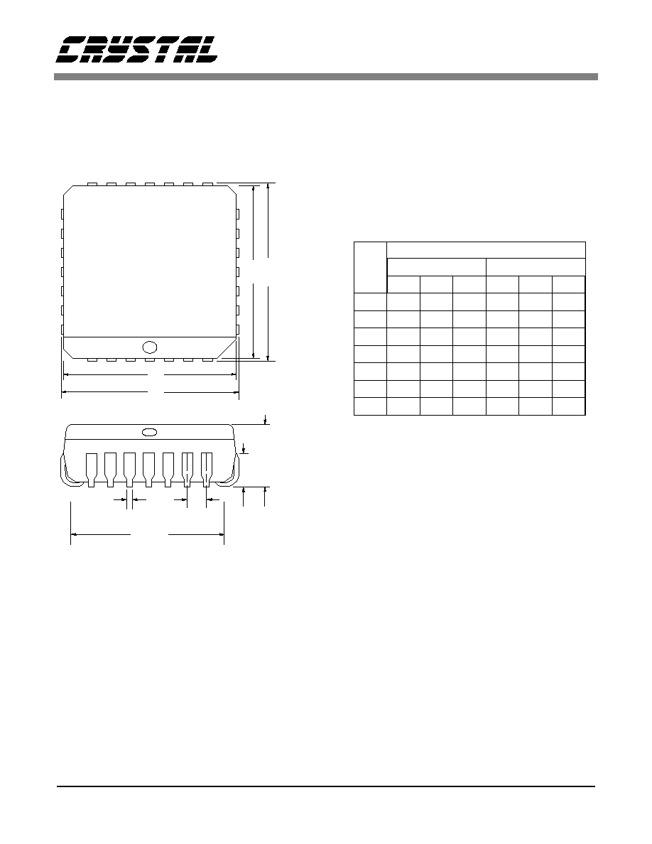
E
E1
D1
D
D2/E2
44 pin
PLCC
NO. OF TERMINALS
D2/E2
MAX
MIN
MAX
MIN
MILLIMETERS
INCHES
DIM
A
D/E
17.65
17.40
0.685
B
e
A
A1
B
e
0.695
16.66
16.51
0.650
0.656
4.57
4.20
0.180
0.165
0.53
0.33
0.021
0.013
2.29
0.090
16.00
14.99
0.590
0.630
1.19
1.35 0.047
0.053
NOM
17.53
16.59
4.45
0.41
2.79
15.50
1.27
NOM
0.690
0.653
0.175
0.016
0.110
0.610
0.050
3.04
0.120
D1/E1
A1

e
MILLIMETERS
INCHES
DIM
D/E
D1/E1
e
b
0.462
0∞
0∞
11.75
MIN
MAX
1.45
MIN
MAX
0.057
10.10
12.25
3.5∞
0.398
0.482
b
A1
A
1.60
0.05
0.063
0.002
c
0.20
0.008
c
0.45
0.75
0.018
0.030
1.35
0.053
9.90
0.390
A1
A
44 PIN TQFP
1
D
D1
E1 E
A2
A2
L
L
0.70
0.45
0.026
0.014
0.036
0.90
0.018
0.30
0.09
0.004
NOM
0.15
0.006
NOM
3.5∞
12.0
0.60
1.40
10.0
0.80
0.37
0.145
0.472
0.024
0.055
0.394
0.031
0.016
0.006
ccc
0.10
0.004
7∞
7∞
ccc
44 LEAD TQFP

∑ Notes ∑

Smart
Analog
TM
is a Trademark of Crystal Semiconductor Corporation