Advance Product Information
This document contains information for a new product.
Cirrus Logic reserves the right to modify this product without notice.
1
Copyright
�
Cirrus Logic, Inc. 2004
(All Rights Reserved)
Cirrus Logic, Inc.
www.cirrus.com
CS42426
114 dB, 192 kHz 6-Ch Codec with PLL
Features
Six 24-bit D/A, two 24-bit A/D converters
114 dB DAC / 114 dB ADC dynamic range
-100 dB THD+N
System sampling rates up to 192 kHz
Integrated low-jitter PLL for increased system
jitter tolerance
PLL clock or OMCK system clock selection
7 configurable general purpose outputs
ADC high pass filter for DC offset calibration
Expandable ADC channels and one-line
mode support
Digital output volume control with soft ramp
Digital +/-15 dB input gain adjust for ADC
Differential analog architecture
Supports logic levels between 5 V and 1.8 V
General Description
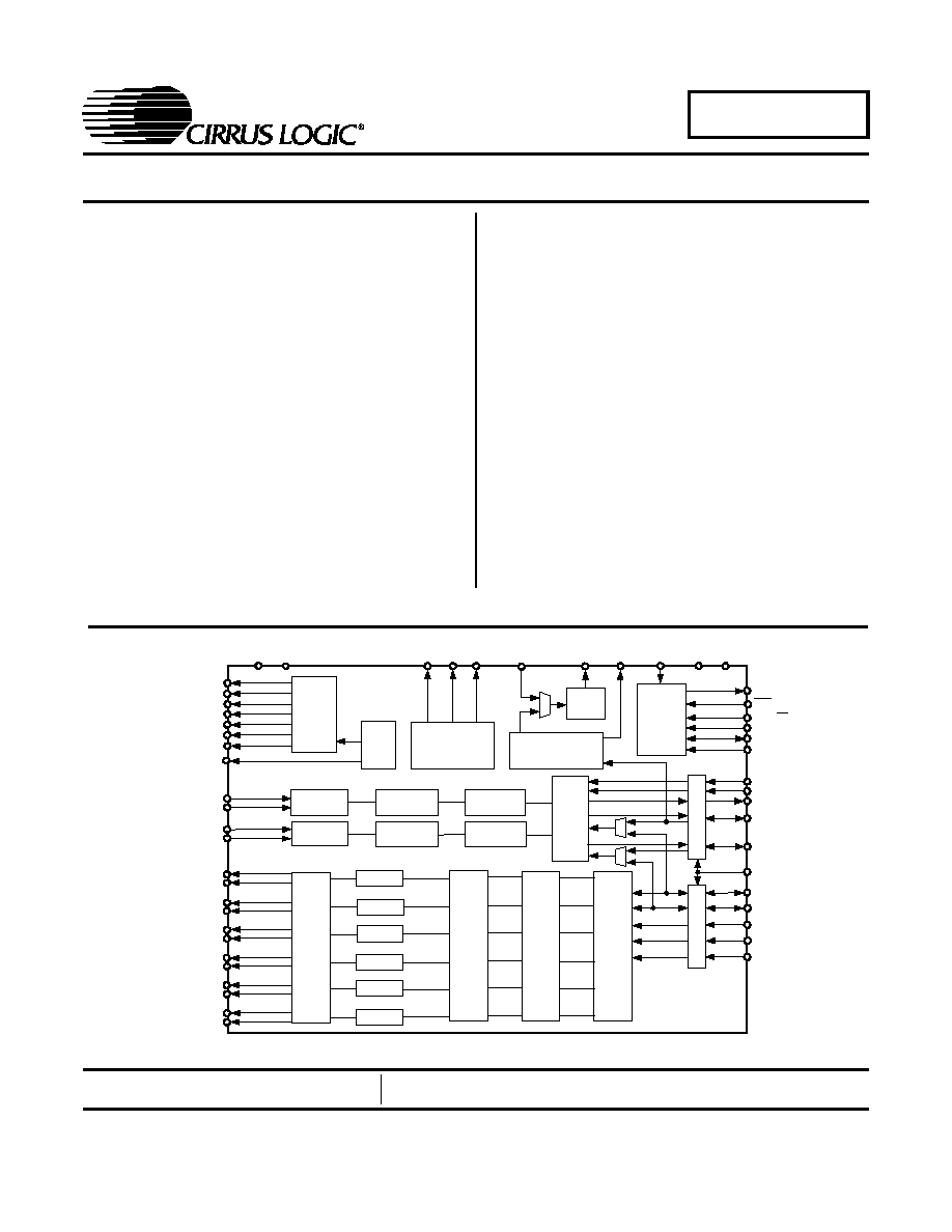
The CS42426 CODEC provides two analog-to-digital and six
digital-to-analog Delta-Sigma converters, as well as an inte-
grated PLL, in a 64-pin LQFP package.
The CS42426 integrated PLL provides a low-jitter system
clock. The internal stereo ADC is capable of independent chan-
nel gain control for single-ended or differential analog inputs.
All six channels of DAC provide digital volume control and dif-
ferential analog outputs. The general purpose outputs may be
driven high or low, or mapped to a variety of DAC mute controls
or ADC overflow indicators.
The CS42426 is ideal for audio systems requiring wide
dynamic range, negligible distortion and low noise, such as A/V
receivers, DVD receivers, digital speaker and automotive audio
systems.
ORDERING INFORMATION
CS42426-CQZ
-10� to 70� C
64-pin LQFP
CS42426-DQZ
-40� to 85� C
64-pin LQFP
CDB42428
Evaluation Board
PLL
Internal Voltage
Reference
RST
GPO1
AD0/CS
SCL/CCLK
SDA/CDOUT
AD1/CDIN
VLC
AOUTA1+
AOUTA1-
AOUTB1+
AOUTA3+
AOUTA3-
AOUTA2-
AOUTB2-
AOUTA2+
AOUTB2+
AOUTB1-
AOUTB3+
AOUTB3-
AINL+
AINL-
AINR+
AINR-
FILT+
REFGND VQ
ADC#1
ADC#2
Digital Filter
Digital Filter
Gain & Clip
Gain & Clip
ADC_SDOUT
ADCIN1
ADCIN2
DAC_SCLK
DAC_LRCK
DAC_SDIN3
DAC_SDIN2
DAC_SDIN1
VLS
ADC_LRCK
DGND VD
OMCK
RMCK
LPFLT
INT
Control
Port
DAC#1
DAC#2
DAC#3
DAC#4
DAC#5
DAC#6
D
i
g
i
t
a
l F
i
lt
e
r
V
o
l
u
m
e
C
ontr
o
l
GPO2
GPO3
GPO4
GPO5
GPO6
GPO7
MUTEC
Mute
A
nal
og F
i
l
t
er
VA AGND
ADC
Serial
Audio
Port
Mult/Div
GPO
ADC_SCLK
Lev
el
T
r
ans
l
ator
Lev
el
T
r
ans
l
a
to
r
DA
C S
e
r
i
al
A
udi
o P
o
r
t
JUL `04
DS604A2

CS42426
2
TABLE OF CONTENTS
1 PIN DESCRIPTIONS ................................................................................................................. 6
2 TYPICAL CONNECTION DIAGRAMS ..................................................................................... 8
3 APPLICATIONS ....................................................................................................................... 10
3.1 Overview .......................................................................................................................... 10
3.2 Analog Inputs ................................................................................................................... 10
3.2.1 Line Level Inputs ................................................................................................. 10
3.2.2 External Input Filter ............................................................................................. 11
3.2.3 High Pass Filter and DC Offset Calibration ......................................................... 11
3.3 Analog Outputs ................................................................................................................ 11
3.3.1 Line Level Outputs and Filtering ......................................................................... 11
3.3.2 Interpolation Filter ............................................................................................... 12
3.3.3 Digital Volume and Mute Control ........................................................................ 12
3.3.4 ATAPI Specification ............................................................................................ 13
3.4 Clock Generation ............................................................................................................. 14
3.4.1 PLL and Jitter Attenuation ................................................................................... 14
3.4.2 OMCK System Clock Mode ................................................................................ 15
3.4.3 Master Mode ....................................................................................................... 15
3.4.4 Slave Mode ......................................................................................................... 15
3.5 Digital Interfaces .............................................................................................................. 16
3.5.1 Serial Audio Interface Signals ............................................................................. 16
3.5.2 Serial Audio Interface Formats ............................................................................ 18
3.5.3 ADCIN1/ADCIN2 Serial Data Format .................................................................. 21
3.5.4 One Line Mode(OLM) Configurations ................................................................. 22
3.6 Control Port Description and Timing ................................................................................ 26
IMPORTANT NOTICE
"Advance" product information describes products that are in development and subject to development changes. Cirrus Logic, Inc. and its subsidiar-
ies ("Cirrus") believe that the information contained in this document is accurate and reliable. However, the information is subject to change without
notice and is provided "AS IS" without warranty of any kind (express or implied). Customers are advised to obtain the latest version of relevant infor-
mation to verify, before placing orders, that information being relied on is current and complete. All products are sold subject to the terms and condi-
tions of sale supplied at the time of order acknowledgment, including those pertaining to warranty, patent infringement, and limitation of liability. No
responsibility is assumed by Cirrus for the use of this information, including use of this information as the basis for manufacture or sale of any items,
or for infringement of patents or other rights of third parties. This document is the property of Cirrus and by furnishing this information, Cirrus grants
no license, express or implied under any patents, mask work rights, copyrights, trademarks, trade secrets or other intellectual property rights. Cirrus
owns the copyrights associated with the information contained herein and gives consent for copies to be made of the information only for use within
your organization with respect to Cirrus integrated circuits or other parts of Cirrus. This consent does not extend to other copying such as copying
for general distribution, advertising or promotional purposes, or for creating any work for resale.
An export permit needs to be obtained from the competent authorities of the Japanese Government if any of the products or technologies described
in this material and controlled under the "Foreign Exchange and Foreign Trade Law" is to be exported or taken out of Japan. An export license and/or
quota needs to be obtained from the competent authorities of the Chinese Government if any of the products or technologies described in this material
is subject to the PRC Foreign Trade Law and is to be exported or taken out of the PRC.
CERTAIN APPLICATIONS USING SEMICONDUCTOR PRODUCTS MAY INVOLVE POTENTIAL RISKS OF DEATH, PERSONAL INJURY, OR
SEVERE PROPERTY OR ENVIRONMENTAL DAMAGE ("CRITICAL APPLICATIONS"). CIRRUS PRODUCTS ARE NOT DESIGNED, AUTHO-
RIZED OR WARRANTED FOR USE IN AIRCRAFT SYSTEMS, MILITARY APPLICATIONS, PRODUCTS SURGICALLY IMPLANTED INTO THE
BODY, LIFE SUPPORT PRODUCTS OR OTHER CRITICAL APPLICATIONS (INCLUDING MEDICAL DEVICES, AIRCRAFT SYSTEMS OR COM-
PONENTS AND PERSONAL OR AUTOMOTIVE SAFETY OR SECURITY DEVICES). INCLUSION OF CIRRUS PRODUCTS IN SUCH APPLICA-
TIONS IS UNDERSTOOD TO BE FULLY AT THE CUSTOMER'S RISK AND CIRRUS DISCLAIMS AND MAKES NO WARRANTY, EXPRESS,
STATUTORY OR IMPLIED, INCLUDING THE IMPLIED WARRANTIES OF MERCHANTABILITY AND FITNESS FOR PARTICULAR PURPOSE,
WITH REGARD TO ANY CIRRUS PRODUCT THAT IS USED IN SUCH A MANNER. IF THE CUSTOMER OR CUSTOMER'S CUSTOMER USES
OR PERMITS THE USE OF CIRRUS PRODUCTS IN CRITICAL APPLICATIONS, CUSTOMER AGREES, BY SUCH USE, TO FULLY INDEMNIFY
CIRRUS, ITS OFFICERS, DIRECTORS, EMPLOYEES, DISTRIBUTORS AND OTHER AGENTS FROM ANY AND ALL LIABILITY, INCLUDING
ATTORNEYS' FEES AND COSTS, THAT MAY RESULT FROM OR ARISE IN CONNECTION WITH THESE USES.
Purchase of I
2
C components of Cirrus Logic, Inc., or one of its sublicensed Associated Companies conveys a license under the Phillips I
2
C Patent Rights to use
those components in a standard I
2
C system.
Cirrus Logic, Cirrus, and the Cirrus Logic logo designs are trademarks of Cirrus Logic, Inc. All other brand and product names in this document may
be trademarks or service marks of their respective owners.
Contacting Cirrus Logic Support
For all product questions and inquiries contact a Cirrus Logic Sales Representative.
To find one nearest you go to
www.cirrus.com/

3
CS42426
3.6.1 SPI Mode ............................................................................................................ 26
3.6.2 I2C Mode ............................................................................................................ 27
3.7 Interrupts ......................................................................................................................... 28
3.8 Reset and Power-up ....................................................................................................... 29
3.9 Power Supply, Grounding, and PCB layout ..................................................................... 29
4 REGISTER QUICK REFERENCE ........................................................................................... 30
5 REGISTER DESCRIPTION ..................................................................................................... 32
5.1 Memory Address Pointer (MAP) ....................................................................................... 32
5.2 Chip I.D. and Revision Register (address 01h) (Read Only) ............................................ 32
5.3 Power Control (address 02h)............................................................................................ 33
5.4 Functional Mode (address 03h) ........................................................................................ 33
5.5 Interface Formats (address 04h) ...................................................................................... 34
5.6 Misc Control (address 05h) .............................................................................................. 36
5.7 Clock Control (address 06h) ............................................................................................. 37
5.8 OMCK/PLL_CLK Ratio (address 07h) (Read Only) ......................................................... 39
5.9 Clock Status (address 08h) (Read Only) .......................................................................... 39
5.10 Volume Control (address 0Dh) ....................................................................................... 40
5.11 Channel Mute (address 0Eh).......................................................................................... 41
5.12 Volume Control (addresses 0Fh, 10h, 11h, 12h, 13h, 14h) ........................................ 42
5.13 Channel Invert (address 17h) ......................................................................................... 42
5.14 Mixing Control Pair 1 (Channels A1 & B1)(address 18h)
Mixing Control Pair 2 (Channels A2 & B2)(address 19h)
Mixing Control Pair 3 (Channels A3 & B3)(address 1Ah) ............................................. 42
5.15 ADC Left Channel Gain (address 1Ch) .......................................................................... 45
5.16 ADC Right Channel Gain (address 1Dh) ........................................................................ 45
5.17 Interrupt Control (address 1Eh) ...................................................................................... 45
5.18 Interrupt Status (address 20h) (Read Only) ................................................................... 46
5.19 Interrupt Mask (address 21h) ......................................................................................... 47
5.20 Interrupt Mode MSB (address 22h)
Interrupt Mode LSB (address 23h)................................................................................ 47
5.21 MuteC Pin Control (address 28h) ................................................................................... 47
5.22 General Purpose Pin Control (addresses 29h to 2Fh) ................................................... 48
6 CHARACTERISTICS AND SPECIFICATIONS ....................................................................... 50
SPECIFIED OPERATING CONDITIONS ............................................................................... 50
ABSOLUTE MAXIMUM RATINGS ......................................................................................... 50
ANALOG INPUT CHARACTERISTICS .................................................................................. 51
A/D DIGITAL FILTER CHARACTERISTICS .......................................................................... 52
ANALOG OUTPUT CHARACTERISTICS .............................................................................. 55
D/A DIGITAL FILTER CHARACTERISTICS .......................................................................... 56
SWITCHING CHARACTERISTICS ........................................................................................ 61
SWITCHING CHARACTERISTICS - CONTROL PORT - I2C FORMAT ............................... 62
SWITCHING CHARACTERISTICS - CONTROL PORT - SPI FORMAT ............................... 63
DC ELECTRICAL CHARACTERISTICS ................................................................................ 64
DIGITAL INTERFACE CHARACTERISTICS ......................................................................... 64
7 PARAMETER DEFINITIONS ................................................................................................... 65
8 REFERENCES ......................................................................................................................... 66
9 PACKAGE DIMENSIONS .................................................................................................... 67
THERMAL CHARACTERISTICS ........................................................................................... 67