
Preliminary Product Information
This document contains information for a new product.
Cirrus Logic reserves the right to modify this product without notice.
Copyright
©
Cirrus Logic, Inc. 2005
(All Rights Reserved)
Cirrus Logic, Inc.
http://www.cirrus.com
FEATURES
Six 24-bit A/D, Six 24-bit D/A Converters
ADC Dynamic Range
≠ 105 dB Differential
≠ 102 dB Single-ended
DAC Dynamic Range
≠ 108 dB Differential
≠ 105 dB Single-ended
ADC/DAC THD+N
≠ -98 dB Differential
≠ -95 dB Single-ended
Compatible with Industry-standard Time
Division Multiplexed (TDM) Serial Interface
DAC Sampling Rates up to 192 kHz
ADC Sampling Rates up to 96 kHz
Programmable ADC High-pass Filter for DC
Offset Calibration
Logarithmic Digital Volume Control
Hardware Mode or Software I≤C & SPI
TM
Supports Logic Levels Between 5 V and
1.8 V
GENERAL DESCRIPTION
The CS42436 CODEC provides six multi-bit analog-to-digi-
tal and
six
multi-bit digital-to-analog Delta-sigma
converters. The CODEC is capable of operation with either
differential or single-ended inputs and outputs, in a
52
-pin
M
QFP package.
Six fully differential, or single-ended, inputs are available on
stereo ADC1, ADC2, and ADC3. When operating in Single-
ended Mode, an internal MUX before ADC3 allows selec-
tion from up to four single-ended inputs. Digital volume
control is provided for each ADC channel, with selectable
overflow detection.
All
six
DAC channels provide digital volume control and can
operate with differential or single-ended outputs.
An auxiliary serial input is available for an additional two
channels of PCM data.
The CS42436 is ideal for audio systems requiring wide dy-
namic range, negligible distortion and low noise, such as
A/V receivers, DVD receivers, and automotive audio
systems.
ORDERING INFORMATION
See page 63
.
Control Port & Serial
Audio Port Supply =
1.8 V to 5 V
Register
Configuration
Internal Voltage
Reference
Reset
T
DM Se
r
i
a
l
In
te
rfa
c
e
Le
v
e
l
T
r
an
s
l
a
t
o
r
Lev
el Trans
lat
o
r
TDM Serial Audio
Input
Digital Supply =
3.3 V
Hardware Mode or
I
2
C/SPI Software Mode
Control Data
Analog Supply =
3.3 V to 5 V
Differential or
Single-Ended
Outputs
6
Input Master
Clock
6
TDM Serial Audio
Output
Multibit
Oversampling
ADC1&2
High Pass
Filter
Differential or
Single-Ended
Analog Inputs
4
Digital
Filters
4
*Optional MUX allows selection from up to 4 single-ended inputs.
Multibit
Oversampling
ADC3
High Pass
Filter
2
Digital
Filters
2
4:
2*
Auxilliary Serial
Audio Input
Volume
Controls
Digital
Filters
Multibit
DAC1-3 and
Analog Filters
Modulators
CS42436
FEB `05
DS647PP2
108 dB, 192 kHz 6-in, 6-out TDM CODEC

2
DS647PP2
TABLE OF CONTENTS
1 PIN DESCRIPTION - SOFTWARE MODE .............................................................................. 6
1.1 Digital I/O Pin Characteristics ............................................................................................ 7
2 PIN DESCRIPTIONS - HARDWARE MODE ...................................................................... 9
3 TYPICAL CONNECTION DIAGRAMS ................................................................................... 11
4 CHARACTERISTICS AND SPECIFICATIONS ....................................................................... 13
SPECIFIED OPERATING CONDITIONS ............................................................................... 13
ABSOLUTE MAXIMUM RATINGS ......................................................................................... 13
ANALOG INPUT CHARACTERISTICS (CS42436-CMZ)....................................................... 14
ANALOG INPUT CHARACTERISTICS (CS42436-DMZ)....................................................... 15
ADC DIGITAL FILTER CHARACTERISTICS ......................................................................... 16
ANALOG OUTPUT CHARACTERISTICS (CS42436-CMZ)................................................... 17
ANALOG OUTPUT CHARACTERISTICS (CS42436-DMZ)................................................... 19
COMBINED DAC INTERPOLATION & ON-CHIP ANALOG FILTER RESPONSE ................ 21
SWITCHING SPECIFICATIONS - ADC/DAC PORT .............................................................. 22
SWITCHING CHARACTERISTICS - AUX PORT................................................................... 23
SWITCHING SPECIFICATIONS - CONTROL PORT - I≤C MODE......................................... 24
SWITCHING SPECIFICATIONS - CONTROL PORT - SPI FORMAT ................................... 25
DC ELECTRICAL CHARACTERISTICS................................................................................. 26
DIGITAL INTERFACE SPECIFICATIONS & CHARACTERISTICS ....................................... 26
5 APPLICATIONS ....................................................................................................................... 27
5.1 Overview .......................................................................................................................... 27
5.2 Analog Inputs ................................................................................................................... 28
5.2.1 Line Level Inputs ................................................................................................. 28
5.2.2 ADC3 Analog Input ............................................................................................. 29
5.2.3 High Pass Filter and DC Offset Calibration ......................................................... 30
5.3 Analog Outputs ................................................................................................................ 31
5.3.1 Initialization ......................................................................................................... 31
5.3.2 Line-level Outputs and Filtering .......................................................................... 31
5.3.3 Digital Volume Control ........................................................................................ 33
5.3.4 De-Emphasis Filter .............................................................................................. 33
5.4 System Clocking .............................................................................................................. 34
5.5 CODEC Digital Interface .................................................................................................. 34
5.5.1 TDM .................................................................................................................... 34
5.5.2 I/O Channel Allocation ........................................................................................ 35
5.6 AUX Port Digital Interface Formats .................................................................................. 36
5.6.1 I≤S ........................................................................................................................ 36
5.6.2 Left Justified ........................................................................................................ 36
5.7 Control Port Description and Timing ................................................................................ 37
5.7.1 SPI Mode ............................................................................................................ 37
5.7.2 I
2
C Mode ............................................................................................................. 38
5.8 Recommended Power-up Sequence ............................................................................... 39
5.8.1 Hardware Mode ................................................................................................... 39
5.8.2 Software Mode .................................................................................................... 39
5.9 Reset and Power-up ....................................................................................................... 39
5.10 Power Supply, Grounding, and PCB layout ................................................................... 40
6 REGISTER QUICK REFERENCE ........................................................................................... 41
7 REGISTER DESCRIPTION ..................................................................................................... 43
7.1 Memory Address Pointer (MAP) ....................................................................................... 43
7.2 Chip I.D. and Revision Register (address 01h) (Read Only) ............................................ 43
7.3 Power Control (address 02h) ............................................................................................ 44
7.4 Functional Mode (address 03h) ........................................................................................ 45

DS647PP2
3
7.5 Miscellaneous Control (address 04h) ............................................................................... 45
7.6 ADC Control & DAC De-emphasis (address 05h) ............................................................ 46
7.7 Transition Control (address 06h) ...................................................................................... 47
7.8 DAC Channel Mute (address 07h) ................................................................................... 49
7.9 AOUTX Volume Control (addresses 08h-0D) ............................................................... 49
7.10 DAC Channel Invert (address 10h) ................................................................................ 50
7.11 AINX Volume Control (address 11h-16h) ....................................................................... 50
7.12 ADC Channel Invert (address 17h) ................................................................................ 50
7.13 Status (address 19h) (Read Only)................................................................................. 51
7.14 Status Mask (address 1Ah) ............................................................................................ 51
8 APPENDIX A: EXTERNAL FILTERS ...................................................................................... 52
8.1 ADC Input Filter ............................................................................................................... 52
8.1.1 Passive Input Filter ............................................................................................. 53
8.1.2 Passive Input Filter w/Attenuation ....................................................................... 53
8.2 DAC Output Filter ............................................................................................................ 55
9 APPENDIX B: ADC FILTER PLOTS ....................................................................................... 56
10 APPENDIX C: DAC FILTER PLOTS ..................................................................................... 58
11 PARAMETER DEFINITIONS ................................................................................................. 60
12 REFERENCES ....................................................................................................................... 61
13 PACKAGE INFORMATION ................................................................................................... 62
13.1 Thermal Characteristics ................................................................................................ 62
14 ORDERING INFORMATION ................................................................................................. 63
15 REVISION HISTORY ............................................................................................................. 64

4
DS647PP2
LIST OF FIGURES
Figure 1. Typical Connection Diagram (Software Mode) .............................................................. 11
Figure 2. Typical Connection Diagram (Hardware Mode) ............................................................. 12
Figure 3. Output Test Load ........................................................................................................... 20
Figure 4. Maximum Loading.......................................................................................................... 20
Figure 5. TDM Serial Audio Interface Timing ................................................................................ 22
Figure 6. Serial Audio Interface Slave Mode Timing ..................................................................... 23
Figure 7. Control Port Timing - I≤C Format.................................................................................... 24
Figure 8. Control Port Timing - SPI Format................................................................................... 25
Figure 9. Full-Scale Input .............................................................................................................. 29
Figure 10. ADC3 Input Topology................................................................................................... 29
Figure 11. Audio Output Initialization Flow Chart .......................................................................... 32
Figure 12. Full-Scale Output ......................................................................................................... 33
Figure 13. De-Emphasis Curve ..................................................................................................... 34
Figure 14. TDM Serial Audio Format............................................................................................. 35
Figure 15. AUX I≤S Format............................................................................................................ 36
Figure 16. AUX Left Justified Format ............................................................................................ 36
Figure 17. Control Port Timing in SPI Mode.................................................................................. 37
Figure 18. Control Port Timing, I≤C Write ...................................................................................... 38
Figure 19. Control Port Timing, I≤C Read...................................................................................... 38
Figure 20. Single to Differential Active Input Filter ........................................................................ 52
Figure 21. Single-Ended Active Input Filter................................................................................... 52
Figure 22. Passive Input Filter....................................................................................................... 53
Figure 23. Passive Input Filter w/Attenuation................................................................................ 54
Figure 24. Active Analog Output Filter .......................................................................................... 55
Figure 25. Passive Analog Output Filter........................................................................................ 55
Figure 26. SSM Stopband Rejection ............................................................................................. 56
Figure 27. SSM Transition Band ................................................................................................... 56
Figure 28. SSM Transition Band (Detail)....................................................................................... 56
Figure 29. SSM Passband Ripple ................................................................................................. 56
Figure 30. DSM Stopband Rejection............................................................................................. 56
Figure 31. DSM Transition Band ................................................................................................... 56
Figure 32. DSM Transition Band (Detail) ...................................................................................... 57
Figure 33. DSM Passband Ripple ................................................................................................. 57
Figure 34. SSM Stopband Rejection ............................................................................................. 58
Figure 35. SSM Transition Band ................................................................................................... 58
Figure 36. SSM Transition Band (detail) ....................................................................................... 58
Figure 37. SSM Passband Ripple ................................................................................................. 58
Figure 38. DSM Stopband Rejection............................................................................................. 58
Figure 39. DSM Transition Band ................................................................................................... 58
Figure 40. DSM Transition Band (detail) ....................................................................................... 59
Figure 41. DSM Passband Ripple ................................................................................................. 59
Figure 42. QSM Stopband Rejection............................................................................................. 59
Figure 43. QSM Transition Band................................................................................................... 59
Figure 44. QSM Transition Band (detail)....................................................................................... 59
Figure 45. QSM Passband Ripple................................................................................................. 59

DS647PP2
5
LIST OF TABLES
Table 1. I/O Power Rails........................................................................................................................ 7
Table 2. Hardware Configurable Settings............................................................................................ 27
Table 3. AIN5 Analog Input Selection.................................................................................................. 30
Table 4. AIN6 Analog Input Selection.................................................................................................. 30
Table 5. MCLK Frequency Settings..................................................................................................... 34
Table 6. Serial Audio Interface Channel Allocations ........................................................................... 35
Table 7. MCLK Frequency Settings..................................................................................................... 45
Table 8. Example AOUT Volume Settings .......................................................................................... 49
Table 9. Example AIN Volume Settings .............................................................................................. 50
Table 10. Revision History................................................................................................................... 64

6
DS647PP2
1 PIN DESCRIPTION - SOFTWARE MODE
Pin Name
#
Pin Description
SCL/CCLK
1
Serial Control Port Clock (Input) - Serial clock for the control port interface.
SDA/CDOUT
2
Serial Control Data I/O
(Input/Output) -
Input/Output for I
2
C data. Output for SPI data.
AD0/CS
3
Address Bit [0]/ Chip Select (Input) - Chip address bit in I
2
C Mode. Control signal used to select
the chip in SPI mode.
AD1/CDIN
4
Address Bit [1]/ SPI Data Input (Input) - Chip address bit in I
2
C Mode. Input for SPI data.
RST
5
Reset (Input) - The device enters a low power mode and all internal registers are reset to their
default settings when low.
VLC
6
Control Port Power (Input) - Determines the required signal level for the control port interface.
See "Digital I/O Pin Characteristics" on page 7.
FS
7
Frame Sync (Input) - Signals the start of a new TDM frame in the TDM digital interface format.
VD
8
Digital Power (Input) - Positive power supply for the digital section.
DGND
9,18 Digital Ground (Input) -
VLS
10
Serial Port Interface Power (Input) - Determines the required signal level for the serial port inter-
faces. See "Digital I/O Pin Characteristics" on page 7.
SCLK
11
Serial Clock (Input) - Serial clock for the serial audio interface. Input frequency must be 256xFs.
MCLK
12
Master Clock (Input) - Clock source for the delta-sigma modulators and digital filters.
ADC_SDOUT
13
Serial Audio Data Output (Output) - TDM output for two's complement serial audio data.
DAC_SDIN
14
DAC Serial Audio Data Input (Input) - TDM Input for two's complement serial audio data.
AUX_LRCK
15
Auxiliary Left/Right Clock (Output) - Determines which channel, Left or Right, is currently active
on the Auxiliary serial audio data line.
SCL/CCLK
6
2
4
8
10
1
3
5
7
9
11
12
14 15 16 17 18 19 20 21 22 23 24 25
33
37
35
31
29
38
36
34
32
30
28
27
52 51 50 49 48 47 46 45 44 43 42 41
VLS
FS
MCLK
VLC
AD1/CDIN
N.C.
AOUT5+
AOU
T
3
+
AGND
VA
AU
X
_
SDI
N
DAC_SDI
N
ADC_SDOUT
AUX_
SCLK
AU
X
_LR
C
K
AD0/CS
AOU
T
4
+
RST
AOUT6+
AO
UT3
-
AOU
T
2
+
AO
UT2
-
AO
UT1
-
AOU
T
1
+
DGND
VD
SCLK
DG
ND
VQ
AOUT6-
AO
UT4
-
13
SDA/CDOUT
26
39
AOUT5-
40
N.C.
N.C.
N.C.
FI
LT
+
VA
AG
ND
AI
N6
+
/
A
I
N
6
A
AI
N6
-
/
AI
N6
B
AI
N3
+
AI
N4
-
AI
N4
+
AI
N5
-
/
AI
N5
B
AI
N3
-
AI
N5
+
/
A
I
N
5
A
AI
N2
-
AI
N2
+
AIN1+
AIN1-
CS42436
DS647PP2
7
1.1
Digital I/O Pin Characteristics
Various pins on the CS42436 are powered from separate power supply rails. The logic level for each input
should adhere to the corresponding power rail and should not exceed the maximum ratings.
AUX_SCLK
16
Auxiliary Serial Clock (Output) - Serial clock for the Auxiliary serial audio interface.
AUX_SDIN
17
Auxiliary Serial Input (Input) - The CS42436 provides an additional serial input for two's comple-
ment serial audio data.
AOUT1 +,-
AOUT2 +,-
AOUT3 +,-
AOUT4 +,-
AOUT5 +,-
AOUT6 +,-
20,19
21,22
24,23
25,26
28,27
29,30
Differential Analog Output (Output) - The full-scale differential analog output level is specified in
the Analog Characteristics specification table. Each positive leg of the differential outputs may also
be used single-ended.
N.C.
31,32
33,34
Not Connected - Do not connect.
AGND
35,48 Analog Ground (Input) -
VQ
36
Quiescent Voltage (Output) - Filter connection for internal quiescent reference voltage.
VA
37,46 Analog Power (Input) - Positive power supply for the analog section.
AIN1 +,-
AIN2 +,-
AIN3 +,-
AIN4 +,-
AIN5 +,-
AIN6 +,-
39,38
41,40
43,42
45,44
50,49
52,51
Differential Analog Input (Input) - Signals are presented differentially to the delta-sigma modula-
tors. The full-scale input level is specified in the Analog Characteristics specification table. Single-
ended inputs may be applied to the positive terminals when the ADCx SINGLE bit is enabled.
Once in Single-Ended Mode, the negative terminal of AIN1-AIN4 must be externally driven to com-
mon mode. See below for a description of AIN5-AIN6 in Single-Ended Mode.
AIN5 A,B
AIN6 A,B
50,49
52,51
Single-Ended Analog Input (Input) - In Single-Ended Mode, an internal analog mux allows selec-
tion between 2 channels for both analog inputs AIN5 and AIN6 (see section 7.6.6-7.6.8 for details).
The unused leg of each input is internally connected to common mode. The full-scale input level is
specified in the Analog Characteristics specification table.
FILT+
47
Positive Voltage Reference (Output) - Positive reference voltage for the internal sampling cir-
cuits.
Power
Rail
Pin Name
SW/(HW)
I/O
Driver
Receiver
VLC
RST
Input
-
1.8 V - 5.0 V, CMOS
SCL/CCLK
(AIN5_MUX)
Input
-
1.8 V - 5.0 V, CMOS, with Hysteresis
SDA/CDOUT
(AIN6_MUX)
Input/
Output
1.8 V - 5.0 V, CMOS/Open Drain
1.8 V - 5.0 V, CMOS, with Hysteresis
AD0/CS
(MFREQ)
Input
-
1.8 V - 5.0 V, CMOS
AD1/CDIN
(ADC3_HPF)
Input
-
1.8 V - 5.0 V, CMOS
VLS
MCLK
Input
-
1.8 V - 5.0 V, CMOS
LRCK
Input
-
1.8 V - 5.0 V, CMOS
SCLK
Input
-
1.8 V - 5.0 V, CMOS
ADC_SDOUT
(ADC3_SINGLE)
Input/
Output
1.8 V - 5.0 V, CMOS
-
DAC_SDIN
Input
-
1.8 V - 5.0 V, CMOS
Table 1. I/O Power Rails

8
DS647PP2
AUX_LRCK
Output
1.8 V - 5.0 V, CMOS
-
AUX_SCLK
Output
1.8 V - 5.0 V, CMOS
-
AUX_SDIN
Input
-
1.8 V - 5.0 V, CMOS
Power
Rail
Pin Name
SW/(HW)
I/O
Driver
Receiver
Table 1. I/O Power Rails
DS647PP2
9
2 PIN DESCRIPTIONS - HARDWARE MODE
Pin Name
#
Pin Description
AIN5_MUX
AIN6_MUX
1
2
Analog Input Multiplexer
(Input) -
Allows selection between the A and B single-ended inputs of
ADC3. See sections 7.6.7 and 7.6.8 for details.
MFREQ
3
MCLK Frequency (Input) - Sets the required frequency range of the input Master Clock. See sec-
tion 5.4 for the appropriate settings.
ADC3_HPF
4
ADC3 High-Pass Filter Freeze (Input) - When this pin is driven high, the internal high-pass filter
will be disabled for ADC3.The current DC offset value will be frozen and continue to be subtracted
from the conversion result. See "ADC Digital Filter Characteristics" on page 16.
RST
5
Reset (Input) - The device enters a low power mode and all internal registers are reset to their
default settings when low.
VLC
6
Control Port Power (Input) - Determines the required signal level for the control port interface.
See "Digital I/O Pin Characteristics" on page 7.
FS
7
Frame Sync (Input) - Signals the start of a new TDM frame in the TDM digital interface format.
VD
8
Digital Power (Input) - Positive power supply for the digital section.
VLS
10
Serial Port Interface Power (Input) - Determines the required signal level for the serial port inter-
faces.
SCLK
11
Serial Clock (Input) - Serial clock for the serial audio interface. Input frequency must be 256xFs.
ADC_SDOUT/
ADC3_SINGLE
13
Serial Audio Data Output (Output) - TDM output for two's complement serial audio data. Start-up
Option for Hardware Mode: Pull-up to VLS enables Single-Ended Mode for AIN5-AIN6.
DAC_SDIN
14
DAC Serial Audio Data Input (Input) - Input for two's complement serial audio data.
AUX_LRCK
15
Auxiliary Left/Right Clock (Output) - Determines which channel, Left or Right, is currently active
on the Auxiliary serial audio data line.
AIN5_MUX
6
2
4
8
10
1
3
5
7
9
11
12
14 15 16 17 18 19 20 21 22 23 24 25
33
37
35
31
29
38
36
34
32
30
28
27
52 51 50 49 48 47 46 45 44 43 42 41
VLS
FS
MCLK
VLC
ADC3_HPF
FI
LT+
N.C.
AOUT5+
A
OUT
3
+
AGND
VA
AU
X_SD
I
N
DA
C_
S
D
I
N
ADC_SDOUT/
ADC3_SINGLE
A
U
X_
SC
L
K
AU
X_L
R
C
K
MFREQ
A
OUT
4
+
RST
AOUT6+
AOUT
3
-
VA
AGND
A
OUT
2
+
AOUT
2
-
AOUT
1
-
A
OUT
1
+
DGND
VD
SCLK
DGND
VQ
AI
N
6
+
/
A
I
N6
A
AI
N
6
-
/
AI
N6
B
AOUT6-
AOUT
4
-
13
AIN6_MUX
26
39
AOUT5-
40
N.C.
N.C.
N.C.
AI
N
3
+
AI
N
4
-
AI
N
4
+
AI
N
5
-
/
AI
N5
B
AI
N
3
-
AI
N
5
+
/
A
I
N5
A
AIN1+
AI
N
2
-
AI
N
2
+
AIN1-
CS42436
10
DS647PP2
AUX_SCLK
16
Auxiliary Serial Clock (Output) - Serial clock for the Auxiliary serial audio interface.
AUX_SDIN
17
Auxiliary Serial Input (Input) - The CS42436 provides an additional serial input for two's comple-
ment serial audio data.
AOUT1 +,-
AOUT2 +,-
AOUT3 +,-
AOUT4 +,-
AOUT5 +,-
AOUT6 +,-
20,19
21,22
24,23
25,26
28,27
29,30
Differential Analog Output (Output) - The full-scale differential analog output level is specified in
the Analog Characteristics specification table. Each positive leg of the differential outputs may also
be used single-ended.
N.C.
31,32
33,34
Not Connected - Do not connect.
AGND
35,48 Analog Ground (Input) -
VQ
36
Quiescent Voltage (Output) - Filter connection for internal quiescent reference voltage.
VA
37,46 Analog Power (Input) - Positive power supply for the analog section.
AIN1 +,-
AIN2 +,-
AIN3 +,-
AIN4 +,-
AIN5 +,-
AIN6 +,-
39,38
41,40
43,42
45,44
50,49
52,51
Differential Analog Input (Input) - Signals are presented differentially to the delta-sigma modula-
tors. The full-scale input level is specified in the Analog Characteristics specification table. Single-
ended inputs may be applied to the positive terminals when the ADCx SINGLE pin is enabled.
Once in Single-Ended Mode, the negative terminal of AIN1-AIN4 must be externally driven to com-
mon mode. See below for a description of AIN5-AIN6 in Single-Ended Mode.
AIN5 A,B
AIN6 A,B
50,49
52,51
Single-Ended Analog Input (Input) - In Single-Ended Mode, an internal analog mux allows selec-
tion between 2 channels for both analog inputs AIN5 and AIN6 (see section 7.6.6-7.6.8 for details).
The unused leg of each input is internally connected to common mode. The full-scale input level is
specified in the Analog Characteristics specification table.
FILT+
47
Positive Voltage Reference (Output) - Positive reference voltage for the internal sampling cir-
cuits.

DS647PP2
11
3 TYPICAL CONNECTION DIAGRAMS
100 µF
0.1 µF
+
+
VQ
FILT+
0.1 µF
4.7 µF
VA
0.01 µF
DGND
Digital Audio
Processor
CS5341
A/D
Converter
VA
VD
AGND
AGND
AIN1+
AIN1-
Connect DGND and AGND at Codec
0.01 µF
+
10 µF
0.01 µF
+3.3 V
+
10 µF
0.01 µF
+1.8 V
to +5.0 V
Analog Input 1
Input
Filter
1
1. See the ADC Input Filter section in the Appendix.
2. See the DAC Output Filter section in the Appendix.
Analog Input 2
Analog Input 3
Analog Input 4
AIN5+/AIN5A
+3.3 V to +5 V
DGND
AIN2+
AIN2-
AIN3+
AIN3-
AIN4+
AIN4-
AIN5-/AIN5B
AIN6+/AIN6A
AIN6-/AIN6B
Analog Input 5
Analog Input 6
Analog Input 5A
Analog Input 5B
Analog Input 6A
Analog Input 6B
Input
Filter
1
AOUT1+
AOUT1-
AOUT2+
AOUT2-
AOUT3+
AOUT3-
AOUT4+
AOUT4-
Analog Output Filter
2
Analog Output Filter
2
Analog Output Filter
2
AOUT5+
AOUT5-
AOUT6+
AOUT6-
Analog Output Filter
2
Analog Output Filter
2
Analog Output Filter
2
Input
Filter
1
Input
Filter
1
Input
Filter
1
Input
Filter
1
Input
Filter
1
Input
Filter
1
Input
Filter
1
Input
Filter
1
0.1 µF
+1.8 V
to +5 V
Micro-
Controller
2 k
2 k
**
**
** Resistors are required for
I
2
C control port operation
17
16
10
15
13
14
7
11
12
3
4
2
1
5
6
9
48
35
18
47
37
51
52
49
50
44
45
42
43
40
41
38
39
30
29
27
28
26
25
23
24
22
21
19
20
46
37
8
VLC
SCL/CCLK
RST
AD0/CS
SDA/CDOUT
AD1/CDIN
VLS
MCLK
AUX_SDIN
DAC_SDIN
FS
SCLK
AUX_SCLK
AUX_LRCK
ADC_SDOUT
Figure 1. Typical Connection Diagram (Software Mode)

12
DS647PP2
100 µF
0.1 µF
+
+
VQ
FILT+
0.1 µF
4.7 µF
VA
0.01 µF
DGND
0.1 µF
Digital Audio
Processor
CS5341
A/D
Converter
VA
VD
AGND
AGND
AIN1+
AIN1-
Connect DGND and AGND at Codec
0.01 µF
+
10 µF
0.01 µF
+3.3 V
+
10 µF
0.01 µF
+1.8 V
to +5.0 V
Analog Input 1
Input
Filter
1
1. See the ADC Input Filter section in the Appendix.
2. See the DAC Output Filter section in the Appendix.
Analog Input 2
Analog Input 3
Analog Input 4
AIN5+/AIN5A
+3.3 V to +5 V
DGND
AIN2+
AIN2-
AIN3+
AIN3-
AIN4+
AIN4-
AIN5-/AIN5B
AIN6+/AIN6A
AIN6-/AIN6B
Analog Input 5
Analog Input 6
Analog Input 5A
Analog Input 5B
Analog Input 6A
Analog Input 6B
VLS
*
*
* MUX configuration settings for AIN5-AIN6. See
the ADC Input MUX section.
Input
Filter
1
AOUT1+
AOUT1-
AOUT2+
AOUT2-
AOUT3+
AOUT3-
AOUT4+
AOUT4-
Analog Output Filter
2
Analog Output Filter
2
Analog Output Filter
2
AOUT5+
AOUT5-
AOUT6+
AOUT6-
Analog Output Filter
2
Analog Output Filter
2
Analog Output Filter
2
Input
Filter
1
Input
Filter
1
Input
Filter
1
Input
Filter
1
Input
Filter
1
Input
Filter
1
Input
Filter
1
Input
Filter
1
17
16
10
15
13
14
7
11
12
3
4
2
1
5
6
9
48
35
18
47
37
51
52
49
50
44
45
42
43
40
41
38
39
30
29
27
28
26
25
23
24
22
21
19
20
46
37
8
AIN5_MUX
AIN6_MUX
ADC3_HPF
RST
MFREQ
VLC
VLS
MCLK
AUX_SDIN
DAC_SDIN
FS
SCLK
AUX_SCLK
AUX_LRCK
ADC_SDOUT/
ADC3_SINGLE
Figure 2. Typical Connection Diagram (Hardware Mode)

DS647PP2
13
4 CHARACTERISTICS AND SPECIFICATIONS
(All Min/Max characteristics and specifications are guaranteed over the Specified Operating Conditions. Typical per-
formance characteristics and specifications are derived from measurements taken at nominal supply voltages and
T
A
= 25∞ C.)
SPECIFIED OPERATING CONDITIONS
(AGND=DGND=0 V, all voltages with respect to ground.)
ABSOLUTE MAXIMUM RATINGS
(AGND = DGND = 0 V; all voltages with respect to ground.)
WARNING: Operation at or beyond these limits may result in permanent damage to the device. Normal operation is
not guaranteed at these extremes.
Notes: 1. Analog input/output performance will slightly degrade at VA = 3.3 V.
2. The ADC_SDOUT may not meet timing requirements in Double-Speed Mode.
3. Any pin except supplies. Transient currents of up to ±100 mA on the analog input pins will not cause SCR
latch-up.
4. The maximum over/under voltage is limited by the input current.
Parameters
Symbol Min Typ
Max
Units
DC Power Supply
Analog
3.3 V
(Note 1)
5.0
V
VA
3.14
4.75
3.3
5
3.47
5.25
V
V
Digital
3.3 V
VD
3.14
3.3
3.47
V
Serial Audio Interface
1.8 V
(Note 2)
2.5 V
3.3 V
5.0 V
VLS
1.71
2.37
3.14
4.75
1.8
2.5
3.3
5
1.89
2.63
3.47
5.25
V
V
V
V
Control Port Interface
1.8 V
2.5 V
3.3 V
5.0 V
VLC
1.71
2.37
3.14
4.75
1.8
2.5
3.3
5
1.89
2.63
3.47
5.25
V
V
V
V
Ambient Temperature
Commercial -CMZ
Automotive
-DMZ
T
A
-10
-40
-
-
+70
+85
∞
C
∞
C
Parameters
Symbol
Min
Max
Units
DC Power Supply
Analog
Digital
Serial Port Interface
Control Port Interface
VA
VD
VLS
VLC
-0.3
-0.3
-0.3
-0.3
6.0
6.0
6.0
6.0
V
V
V
V
Input Current
(Note 3)
I
in
-
±10
mA
Analog Input Voltage
(Note 4)
V
IN
AGND-0.7
VA+0.7
V
Digital Input Voltage
Serial Port Interface
(Note 4)
Control Port Interface
V
IND-S
V
IND-C
-0.3
-0.3
VLS+ 0.4
VLC+ 0.4
V
V
Ambient Operating Temperature
CS42436-CMZ
(power applied)
CS42436-DMZ
T
A
-20
-50
+85
+95
∞C
∞C
Storage Temperature
T
stg
-65
+150
∞C
14
DS647PP2
ANALOG INPUT CHARACTERISTICS (CS42436-CMZ)
(Test Conditions (unless otherwise specified): VLS = VLC = VD = 3.3 V, VA = 5 V; Full scale input sine wave: 1 kHz
through the active input filter on page 52; Measurement Bandwidth is 10 Hz to 20 kHz unless otherwise specified.)
Differential
Single-Ended
Parameter
Min Typ Max
Min Typ Max
Unit
Single Speed Mode Fs=48 kHz
Dynamic Range
A-weighted
unweighted
99
96
105
102
-
-
96
93
102
99
-
-
dB
dB
Total Harmonic Distortion + Noise
-1 dB
(Note 5)
-20 dB
-60 dB
-
-
-
-98
-82
-42
-92
-
-
-
-
-
-95
-79
-39
-89
-
-
dB
dB
dB
Double Speed Mode Fs=96 kHz
Dynamic Range
A-weighted
unweighted
40 kHz bandwidth unweighted
99
96
-
105
102
99
-
-
-
96
93
102
99
96
-
-
-
dB
dB
dB
Total Harmonic Distortion + Noise
-1 dB
(Note 5)
-20 dB
-60 dB
40 kHz bandwidth -1 dB
-
-
-
-
-98
-82
-42
-90
-92
-
-
-
-
-
-
-
-95
-79
-39
-90
-89
-
-
-
dB
dB
dB
dB
All Speed Modes
ADC1-3 Interchannel Isolation
-
90
-
-
90
-
dB
ADC3 MUX Interchannel Isolation
-
90
-
-
90
-
dB
DC Accuracy
Interchannel Gain Mismatch
-
0.1
-
-
0.1
-
dB
Gain Drift
-
±100
-
-
±100
-
ppm/∞C
Analog Input
Full-scale Input Voltage
1.06*VA 1.12*VA 1.18*VA 0.53*VA 0.56*VA 0.59*VA
Vpp
Differential Input Impedance
(Note 6)
18
-
-
-
-
-
k
Single-Ended Input Impedance
(Note 7)
-
-
-
18
-
-
k
Common Mode Rejection Ratio (CMRR)
-
82
-
-
-
-
dB

DS647PP2
15
ANALOG INPUT CHARACTERISTICS (CS42436-DMZ)
(Test Conditions (unless otherwise specified):VLS = VLC = VD = 3.3 V, VA = 5 V; Full scale input sine wave: 1 kHz
through the active input filter on page 52; Measurement Bandwidth is 10 Hz to 20 kHz unless otherwise specified.)
Notes: 5. Referred to the typical full-scale voltage.
6. Measured between AINx+ and AINx-.
7. Measured between AINxx and AGND.
Differential
Single-Ended
Parameter
Min Typ Max
Min Typ Max
Unit
Single Speed Mode Fs=48 kHz
Dynamic Range
A-weighted
unweighted
97
94
105
102
-
-
94
91
102
99
-
-
dB
dB
Total Harmonic Distortion + Noise
-1 dB
(Note 5)
-20 dB
-60 dB
-
-
-
-98
-82
-42
-90
-
-
-
-
-
-95
-79
-39
-87
-
-
dB
dB
dB
Double Speed Mode Fs=96 kHz
Dynamic Range
A-weighted
unweighted
40 kHz bandwidth unweighted
97
94
-
105
102
99
-
-
-
94
91
-
102
99
96
-
-
-
dB
dB
dB
Total Harmonic Distortion + Noise
-1 dB
(Note 5)
-20 dB
-60 dB
40 kHz bandwidth -1 dB
-
-
-
-
-98
-82
-42
-87
-90
-
-
-
-
-
-
-
-95
-79
-39
-87
-87
-
-
-
dB
dB
dB
dB
All Speed Modes
ADC1-3 Interchannel Isolation
-
90
-
-
90
-
dB
ADC3 MUX Interchannel Isolation
-
85
-
-
85
-
dB
DC Accuracy
Interchannel Gain Mismatch
-
0.1
-
-
0.1
-
dB
Gain Drift
-
±100
-
-
±100
-
ppm/∞C
Analog Input
Full-scale Input Voltage
1.04*VA 1.12*VA 1.20*VA 0.52*VA 0.56*VA 0.60*VA
Vpp
Differential Input Impedance
(Note 6)
18
-
-
-
-
-
k
Single-Ended Input Impedance
(Note 7)
-
-
-
18
-
-
k
Common Mode Rejection Ratio (CMRR)
-
82
-
-
-
-
dB
16
DS647PP2
ADC DIGITAL FILTER CHARACTERISTICS
Notes: 8. Filter response is guaranteed by design.
9. Response is clock dependent and will scale with Fs. Note that the response plots (Figures 26 to 33) have
been normalized to Fs and can be de-normalized by multiplying the X-axis scale by Fs.
Parameter (Note 8, 9)
Min
Typ
Max
Unit
Single Speed Mode
(Note 9)
Passband (Frequency Response)
to -0.1 dB corner
0
-
0.4896
Fs
Passband Ripple
-
-
0.08
dB
Stopband
0.5688
-
-
Fs
Stopband Attenuation
70
-
-
dB
Total Group Delay
-
12/Fs
-
s
Double Speed Mode
(Note 9)
Passband (Frequency Response)
to -0.1 dB corner
0
-
0.4896
Fs
Passband Ripple
-
-
0.16
dB
Stopband
0.5604
-
-
Fs
Stopband Attenuation
69
-
-
dB
Total Group Delay
-
9/Fs
-
s
High Pass Filter Characteristics
Frequency Response -3.0 dB
-0.13 dB
-
1
20
-
-
Hz
Hz
Phase Deviation
@ 20 Hz
-
10
-
Deg
Passband Ripple
-
-
0
dB
Filter Settling Time
-
10
5
/Fs
0
s

DS647PP2
17
ANALOG OUTPUT CHARACTERISTICS (CS42436-CMZ)
(Test Conditions (unless otherwise specified):VLS = VLC = VD = 3.3 V, VA = 5 V; Measurement Bandwidth is
10 Hz to 20 kHz unless otherwise specified; Full scale 997 Hz output sine wave (see Note 11); Single-ended test
load: R
L
= 3 k
, C
L
= 10 pF.)
Parameter
Differential
Min Typ Max
Single-Ended
Min Typ Max
Unit
Single-Speed Mode Fs = 48 kHz
Dynamic Range
18 to 24-Bit
A-weighted
unweighted
16-Bit
A-weighted
unweighted
102
99
-
-
108
105
99
96
-
-
-
-
99
96
-
-
105
102
96
93
-
-
-
-
dB
dB
dB
dB
Total Harmonic Distortion + Noise
18 to 24-Bit
0 dB
-20 dB
-60 dB
16-Bit
0 dB
-20 dB
-60 dB
-
-
-
-
-
-
-98
-85
-45
-93
-76
-36
-92
-
-
-
-
-
-
-
-
-
-
-95
-82
-42
-90
-73
-33
-89
-
-
-
-
-
dB
dB
dB
dB
dB
dB
Double-Speed Mode Fs = 96 kHz
Dynamic Range
18 to 24-Bit
A-weighted
unweighted
16-Bit
A-weighted
unweighted
102
99
-
-
108
105
99
96
-
-
-
-
99
96
-
-
105
102
96
93
-
-
-
-
dB
dB
dB
dB
Total Harmonic Distortion + Noise
18 to 24-Bit
0 dB
-20 dB
-60 dB
16-Bit
0 dB
-20 dB
-60 dB
-
-
-
-
-
-
-98
-85
-45
-93
-76
-36
-92
-
-
-
-
-
-
-
-
-
-
-95
-82
-42
-90
-73
-33
-89
-
-
-
-
-
dB
dB
dB
dB
dB
dB
Quad-Speed Mode Fs = 192 kHz
Dynamic Range
18 to 24-Bit
A-weighted
unweighted
16-Bit
A-weighted
unweighted
102
99
-
-
108
105
99
96
-
-
-
-
99
96
-
-
105
102
96
93
-
-
-
-
dB
dB
dB
dB
Total Harmonic Distortion + Noise
18 to 24-Bit
0 dB
-20 dB
-60 dB
16-Bit
0 dB
-20 dB
-60 dB
-
-
-
-
-
-
-98
-85
-45
-93
-76
-36
-92
-
-
-
-
-
-
-
-
-
-
-95
-82
-42
-90
-73
-33
-89
-
-
-
-
-
dB
dB
dB
dB
dB
dB

18
DS647PP2
All Speed Modes
Interchannel Isolation (1 kHz)
-
100
-
-
100
-
dB
Analog Output
Full Scale Output
1.235∑VA 1.300∑VA 1.365∑VA 0.618∑VA 0.650∑VA 0.683∑VA
Vpp
Interchannel Gain Mismatch
-
0.1
0.25
-
0.1
0.25
dB
Gain Drift
-
±100
-
-
±100
-
ppm/∞C
Output Impedance
-
100
-
-
100
-
DC Current draw from an AOUT pin
(Note 10)
-
-
10
-
-
10
µ
A
AC-Load Resistance (R
L
)
(Note 12)
3
-
-
3
-
-
k
Load Capacitance (C
L
)
(Note 12)
-
-
100
-
-
100
pF
DS647PP2
19
ANALOG OUTPUT CHARACTERISTICS (CS42436-DMZ)
(Test Conditions (unless otherwise specified): VLS = VLC = VD = 3.3 V,VA = 5 V; Measurement Bandwidth is
10 Hz to 20 kHz unless otherwise specified; Full scale 997 Hz output sine wave (see Note 11); Single-ended test
load: R
L
= 3 k
, C
L
= 10 pF.)
Parameter
Differential
Min Typ Max
Single-Ended
Min Typ Max
Unit
Single-Speed Mode Fs = 48 kHz
Dynamic Range
18 to 24-Bit
A-weighted
unweighted
16-Bit
A-weighted
unweighted
100
97
-
-
108
105
99
96
-
-
-
-
97
94
-
-
105
102
96
93
-
-
-
-
dB
dB
dB
dB
Total Harmonic Distortion + Noise
18 to 24-Bit
0 dB
-20 dB
-60 dB
16-Bit
0 dB
-20 dB
-60 dB
-
-
-
-
-
-
-98
-85
-45
-93
-76
-36
-90
-
-
-
-
-
-
-
-
-
-
-
-95
-82
-42
-90
-73
-33
-87
-
-
-
-
-
dB
dB
dB
dB
dB
dB
Double-Speed Mode Fs = 96 kHz
Dynamic Range
18 to 24-Bit
A-weighted
unweighted
16-Bit
A-weighted
unweighted
100
97
-
-
108
105
99
96
-
-
-
-
97
94
-
-
105
102
96
93
-
-
-
-
dB
dB
dB
dB
Total Harmonic Distortion + Noise
18 to 24-Bit
0 dB
-20 dB
-60 dB
16-Bit
0 dB
-20 dB
-60 dB
-
-
-
-
-
-
-98
-85
-45
-93
-76
-36
-90
-
-
-
-
-
-
-
-
-
-
-
-95
-82
-42
-90
-73
-33
-87
-
-
-
-
-
dB
dB
dB
dB
dB
dB
Quad-Speed Mode Fs = 192 kHz
Dynamic Range
18 to 24-Bit
A-weighted
unweighted
16-Bit
A-weighted
unweighted
100
97
-
-
108
105
99
96
-
-
-
-
97
94
-
-
105
102
96
93
-
-
-
-
dB
dB
dB
dB
Total Harmonic Distortion + Noise
18 to 24-Bit
0 dB
-20 dB
-60 dB
16-Bit
0 dB
-20 dB
-60 dB
-
-
-
-
-
-
-98
-85
-45
-93
-76
-36
-90
-
-
-
-
-
-
-
-
-
-
-
-95
-82
-42
-90
-73
-33
-87
-
-
-
-
-
dB
dB
dB
dB
dB
dB
20
DS647PP2
Notes: 10. Guaranteed by design. The DC current draw represents the allowed current draw from the AOUT pin
due to typical leakage through the electrolytic DC blocking capacitors.
11. One-half LSB of triangular PDF dither is added to data.
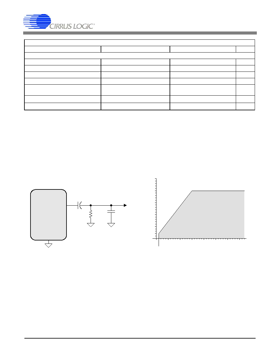
12. Guaranteed by design. See Figure 3. R
L
and C
L
reflect the recommended minimum resistance and
maximum capacitance required for the internal op-amp's stability and signal integrity. In this circuit
topology, C
L
will effectively move the dominant pole of the two-pole amp in the output stage. Increasing
this value beyond the recommended 100 pF can cause the internal op-amp to become unstable. See
Appendix A for a recommended output filter.
All Speed Modes
Interchannel Isolation (1 kHz)
-
100
-
-
100
-
dB
Analog Output
Full Scale Output
1.210∑VA 1.300∑VA 1.392∑VA 0.605∑VA 0.650∑VA 0.696∑VA
Vpp
Interchannel Gain Mismatch
-
0.1
0.25
-
0.1
0.25
dB
Gain Drift
-
±100
-
-
±100
-
ppm/∞C
Output Impedance
-
100
-
-
100
-
DC Current draw from an AOUT pin
(Note 10)
-
-
10
-
-
10
µ
A
AC-Load Resistance (R
L
)
(Note 12)
3
-
-
3
-
-
k
Load Capacitance (C
L
)
(Note 12)
-
-
100
-
-
100
pF
100
50
75
25
2.5
5
10
15
Safe Operating
Region
C
a
p
a
ci
t
i
ve
L
oad -
-
C
(
p
F
)
L
Resistive Load -- R (k
)
L
125
3
20
AOUTxx
3.3 µF
Analog
Output
C
L
+
R
L
DAC1-3
AGND
Figure 3. Output Test Load
Figure 4. Maximum Loading

DS647PP2
21
COMBINED DAC INTERPOLATION & ON-CHIP ANALOG FILTER RESPONSE
Notes: 13. Response is clock dependent and will scale with Fs. Note that the response plots (Figures 34 to 45) have
been normalized to Fs and can be de-normalized by multiplying the X-axis scale by Fs.
14. Single and Double Speed Mode Measurement Bandwidth is from Stopband to 3 Fs.
Quad Speed Mode Measurement Bandwidth is from Stopband to 1.34 Fs.
15. De-emphasis is only available in Single Speed Mode.
Parameter (Note 8, 13)
Min
Typ
Max
Unit
Single Speed Mode
Passband (Frequency Response)
to -0.05 dB corner
to -3 dB corner
0
0
-
-
0.4780
0.4996
Fs
Fs
Frequency Response 10 Hz to 20 kHz
-0.2
-
+0.08
dB
StopBand
0.5465
-
-
Fs
StopBand Attenuation
(Note 14)
50
-
-
dB
Group Delay
-
10/Fs
-
s
De-emphasis Error (Note 15)
Fs = 32 kHz
Fs = 44.1 kHz
Fs = 48 kHz
-
-
-
-
-
-
+1.5/+0
+0.05/-0.25
-0.2/-0.4
dB
dB
dB
Double Speed Mode
Passband (Frequency Response)
to -0.1 dB corner
to -3 dB corner
0
0
-
-
0.4650
0.4982
Fs
Fs
Frequency Response 10 Hz to 20 kHz
-0.2
-
+0.7
dB
StopBand
0.5770
-
-
Fs
StopBand Attenuation
(Note 14)
55
-
-
dB
Group Delay
-
5/Fs
-
s
Quad Speed Mode
Passband (Frequency Response)
to -0.1 dB corner
to -3 dB corner
0
0
-
-
0.397
0.476
Fs
Fs
Frequency Response 10 Hz to 20 kHz
-0.2
-
+0.05
dB
StopBand
0.7
-
-
Fs
StopBand Attenuation
(Note 14)
51
-
-
dB
Group Delay
-
2.5/Fs
-
s

22
DS647PP2
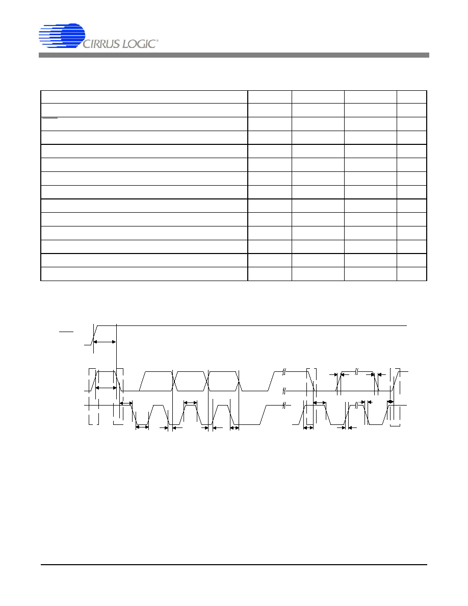
SWITCHING SPECIFICATIONS - ADC/DAC PORT
(Inputs: Logic 0 = DGND, Logic 1 = VLS,
ADC_SDOUT C
LOAD
= 15 pF.)
Notes: 16. After powering up the CS42436, RST should be held low after the power supplies and clocks are settled.
17. See Table 7 on page 45 for suggested MCLK frequencies.
18. VLS is limited to nominal 2.5 V to 5.0 V operation only.
19. ADC does not meet timing specification for Quad-Speed Mode.
Parameters Symbol
Min
Max
Units
Slave Mode
RST pin Low Pulse Width
(Note 16)
1
-
ms
MCLK Frequency
0.512
50
MHz
MCLK Duty Cycle
(Note 17)
45
55
%
Input Sample Rate (FS pin)
Single-Speed Mode
Double-Speed Mode
(Note 18)
Quad-Speed Mode
(Note 19)
F
s
F
s
F
s
4
50
100
50
100
200
kHz
kHz
kHz
SCLK Duty Cycle
45
55
%
SCLK High Time
t
sckh
8
-
ns
SCLK Low Time
t
sckl
8
-
ns
FS Rising Edge to SCLK Rising Edge
t
fss
5
-
ns
SCLK Rising Edge to FS Falling Edge
t
fsh
16
-
ns
DAC_SDIN Setup Time Before SCLK Rising Edge
t
ds
3
-
ns
DAC_SDIN Hold Time After SCLK Rising Edge
t
dh
5
-
ns
DAC_SDIN Hold Time After SCLK Rising Edge
t
dh1
5
-
ns
ADC_SDOUT Hold Time After SCLK Rising Edge
t
dh2
10
-
ns
ADC_SDOUT Valid Before SCLK Rising Edge
t
dval
15
-
ns
ADC_SDOUT
DAC_SDIN
t
ds
SCLK
(input)
FS
(input)
MSB
t
dh1
t
sckh
t
sckl
t
dval
MSB-1
MSB
MSB-1
t
fsh
t
fss
t
dh2
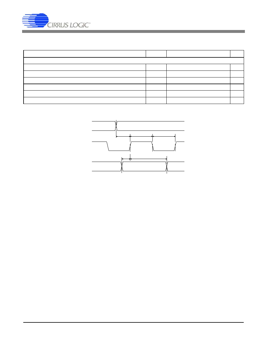
Figure 5. TDM Serial Audio Interface Timing
DS647PP2
23
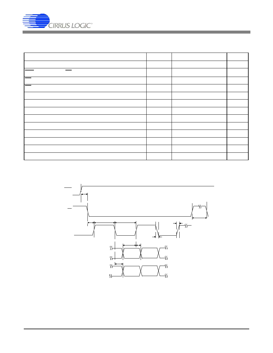
SWITCHING CHARACTERISTICS - AUX PORT
(Inputs: Logic 0 = DGND, Logic 1 = VLS.)
Parameters
Symbol Min
Max
Units
Master Mode
Output Sample Rate (AUX_LRCK) All
Speed
Modes
F
s
-
LRCK
kHz
AUX_SCLK Frequency
-
64
∑
LRCK
kHz
AUX_SCLK Duty Cycle
45
55
%
AUX_LRCK Edge to SCLK Rising Edge
t
lcks
-
5
ns
AUX_SDIN Setup Time Before SCLK Rising Edge
t
ds
3
-
ns
AUX_SDIN Hold Time After SCLK Rising Edge
t
dh
5
-
ns
AUX_SDIN
AUX_SCLK
AUX_LRCK
t
sckh
t
sckl
t
lcks
t
ds
MSB
t
dh
MSB-1
Figure 6. Serial Audio Interface Slave Mode Timing
24
DS647PP2
SWITCHING SPECIFICATIONS - CONTROL PORT - I≤C MODE
(VLC = 1.8 V - 5.0 V, VLS = VD = 3.3 V, VA = 5.0 V; Inputs: Logic 0 = DGND, Logic 1 = VLC, SDA C
L
= 30 pF)
Notes: 20. Data must be held for sufficient time to bridge the transition time, t
fc
, of SCL.
21. Guaranteed by design.
Parameter Symbol
Min
Max
Unit
SCL Clock Frequency
f
scl
-
100
kHz
RST Rising Edge to Start
t
irs
500
-
ns
Bus Free Time Between Transmissions
t
buf
4.7
-
µs
Start Condition Hold Time (prior to first clock pulse)
t
hdst
4.0
-
µs
Clock Low time
t
low
4.7
-
µs
Clock High Time
t
high
4.0
-
µs
Setup Time for Repeated Start Condition
t
sust
4.7
-
µs
SDA Hold Time from SCL Falling
(Note 20)
t
hdd
0
-
µs
SDA Setup time to SCL Rising
t
sud
250
-
ns
Rise Time of SCL and SDA
(Note 21)
t
rc
-
1
µs
Fall Time SCL and SDA
(Note 21)
t
fc
-
300
ns
Setup Time for Stop Condition
t
susp
4.7
-
µs
Acknowledge Delay from SCL Falling
t
ack
300
1000
ns
t buf
t hdst
t
lo w
t
hdd
t high
t sud
Stop
Start
S D A
S C L
t irs
R S T
t
hdst
t rc
t fc
t sust
t susp
Sta rt
Stop
R e pe ate d
t rd
t fd
t ack
Figure 7. Control Port Timing - I≤C Format
DS647PP2
25
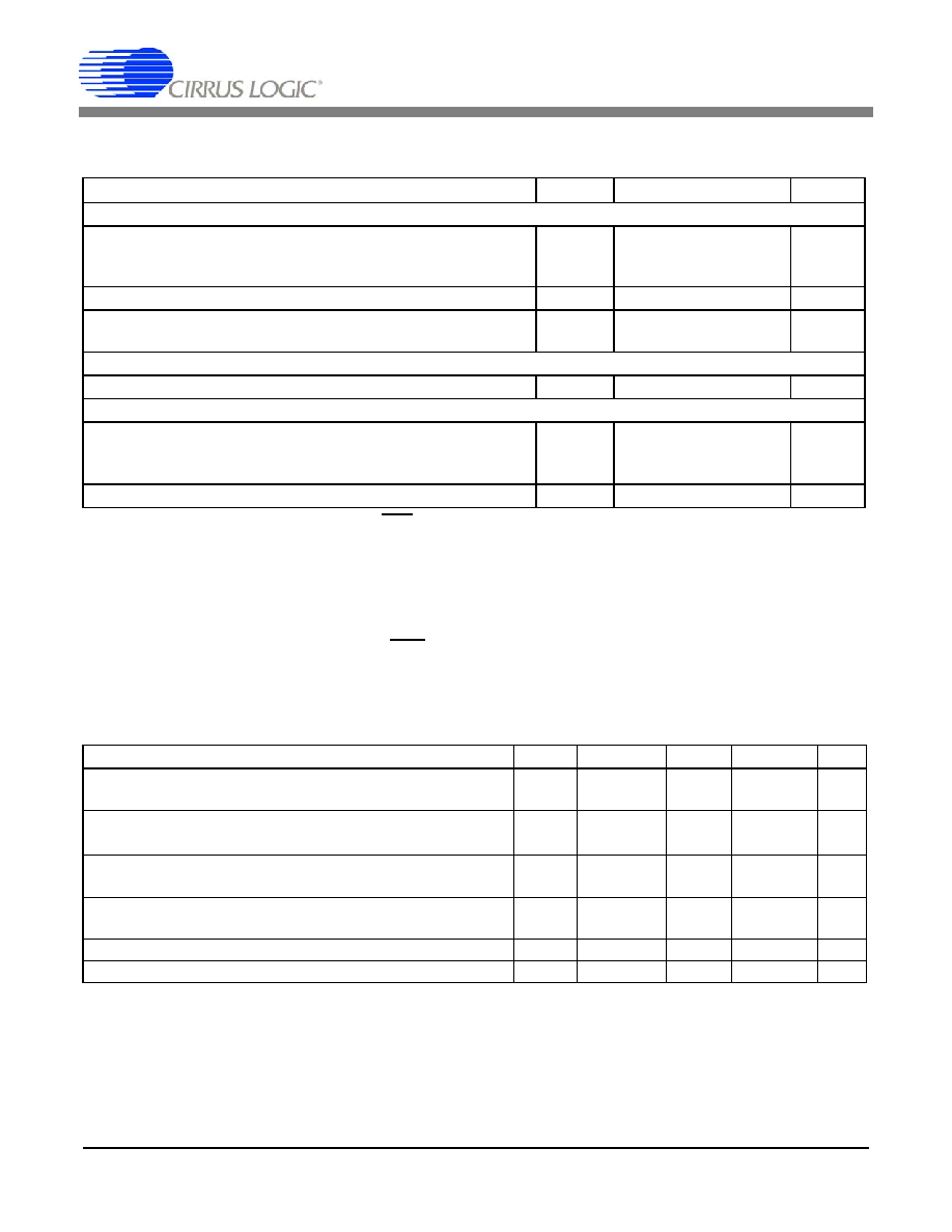
SWITCHING SPECIFICATIONS - CONTROL PORT - SPI FORMAT
(VLC = 1.8 V - 5.0 V, VLS = VD = 3.3 V, VA = 5.0 V; Inputs: Logic 0 = DGND, Logic 1 = VLC, CDOUT C
L
= 30 pF)
Notes: 22. Data must be held for sufficient time to bridge the transition time of CCLK.
23. For f
sck
<1 MHz.
Parameter
Symbol Min Max
Units
CCLK Clock Frequency
f
sck
0
6.0
MHz
RST Rising Edge to CS Falling
t
srs
20
-
ns
CS Falling to CCLK Edge
t
css
20
-
ns
CS High Time Between Transmissions
t
csh
1.0
-
µ
s
CCLK Low Time
t
scl
66
-
ns
CCLK High Time
t
sch
66
-
ns
CDIN to CCLK Rising Setup Time
t
dsu
40
-
ns
CCLK Rising to DATA Hold Time
(Note 22)
t
dh
15
-
ns
CCLK Falling to CDOUT Stable
t
pd
-
50
ns
Rise Time of CDOUT
t
r1
-
25
ns
Fall Time of CDOUT
t
f1
-
25
ns
Rise Time of CCLK and CDIN
(Note 23)
t
r2
-
100
ns
Fall Time of CCLK and CDIN
(Note 23)
t
f2
-
100
ns
CS
CCLK
CDIN
CDOUT
RST
t
srs
t
scl
t
sch
t
css
t
r2
t
f2
t
csh
t
dsu
t
dh
MSB
MSB
t
pd
Figure 8. Control Port Timing - SPI Format
26
DS647PP2
DC ELECTRICAL CHARACTERISTICS
(AGND = 0 V; all voltages with respect to ground.)
Notes: 24. Normal operation is defined as RST = HI with a 997 Hz, 0 dBFS input to the DAC and AUX port, and a
1 kHz, -1 dB analog input to the ADC port sampled at the highest F
s
for each speed mode. DAC outputs
are open, unless otherwise specified.
25. I
DT
measured with no external loading on pin 2 (SDA).
26. Valid with the recommended capacitor values on FILT+ and VQ. Increasing the capacitance will also
increase the PSRR.
27. Power Down Mode is defined as RST = LO with all clocks and data lines held static and no analog input.
28. Guaranteed by design. The DC current draw represents the allowed current draw from the VQ pin due
to typical leakage through the electrolytic de-coupling capacitors.
DIGITAL INTERFACE SPECIFICATIONS & CHARACTERISTICS
Notes: 29. See
"Digital I/O Pin Characteristics" on page 7
for serial and control port power rails.
Parameters
Symbol
Min
Typ
Max
Units
Normal Operation
(Note 24)
Power Supply Current
VA = 5.0 V
VLS = VLC = VD = 3.3 V
(Note 25)
I
A
I
DT
-
-
80
60.6
-
-
mA
mA
Power Dissipation
VLS = VLC = VD = 3.3 V, VA = 5 V
-
600
850
mW
Power Supply Rejection Ratio
1 kHz
(Note 26)
60 Hz
PSRR
-
-
60
40
-
-
dB
dB
Power-down Mode
(Note 27)
Power Dissipation
VLS = VLC = VD = 3.3 V, VA = 5 V
-
1.25
-
mW
VQ Characteristics
Nominal Voltage
Output Impedance
DC current source/sink
(Note 28)
-
-
-
0.5∑VA
23
-
-
-
10
V
k
µ
A
FILT+ Nominal Voltage
-
VA
-
V
Parameters
(Note 29)
Symbol Min Typ
Max
Units
High-Level Output Voltage at I
o
=2 mA
Serial Port
Control Port
V
OH
VLS-1.0
VLC-1.0
-
-
-
-
V
V
Low-Level Output Voltage at I
o
=2 mA
Serial Port
Control Port
V
OL
-
-
-
-
0.4
0.4
V
V
High-Level Input Voltage
Serial Port
Control Port
V
IH
0.7xVLS
0.7xVLC
-
-
-
-
V
V
Low-Level Input Voltage
Serial Port
Control Port
V
IL
-
-
-
-
0.2xVLS
0.2xVLC
V
V
Input Leakage Current
I
in
-
-
±10
µ
A
Input Capacitance
(Note 21)
-
-
10
pF

DS647PP2
27
5 APPLICATIONS
5.1
Overview
The CS42436 is a highly integrated mixed signal 24-bit audio CODEC comprised of 6 analog-to-digital
converters (ADC), implemented using multi-bit delta-sigma techniques, and 6 digital-to-analog converters
(DAC) also implemented using multi-bit delta-sigma techniques.
Other functions integrated within the CODEC include independent digital volume controls for each DAC,
digital de-emphasis filters for the DAC, digital volume control with gain on each ADC channel, ADC high-
pass filters, and an on-chip voltage reference.
The serial audio interface ports allow up to 6 DAC channels and 8 ADC channels in a Time-Division Mul-
tiplexed (TDM) interface format. The CS42436 features an Auxiliary Port used to accommodate an addi-
tional two channels of PCM data on the ADC_SDOUT data line in the TDM digital interface format. See
"AUX Port Digital Interface Formats" on page 36 for details.
The CS42436 operates in one of three oversampling modes based on the input sample rate. Mode selec-
tion is determined automatically based on the MCLK frequency setting. Single-Speed mode (SSM) sup-
ports input sample rates up to 50 kHz and uses a 128x oversampling ratio. Double-Speed mode (DSM)
supports input sample rates up to 100 kHz and uses an oversampling ratio of 64x. Quad-Speed mode
(QSM) supports input sample rates up to 200 kHz and uses an oversampling ratio of 32x (NOTE: QSM
for the ADC is only supported in the I≤S, Left-Justified, Right-Justified interface formats. QSM is not sup-
ported for the ADC). NOTE: QSM is only available in software mode (see section 5.4 on page 34 for de-
tails).
All functions can be configured through software via a serial control port operable in SPI mode or in I≤C
mode. A hardware, stand-alone mode is also available, allowing configuration of the CODEC on a more
limited basis. See Table 2 for the default configuration in Hardware Mode.
Figure 1 on page 11 and Figure 2 on page 12 show the recommended connections for the CS42436
in
software and hardware mode, respectively. See section "Register Description" on page 43 for the default
register settings and options in Software Mode.
Hardware Mode Feature Summary
Function
Default Configuration
Hardware Control
Note
Power Down ADC
All ADC's are enabled
-
-
Power Down DAC
All DAC's are enabled
-
-
Power Down Device
Device is powered up
-
-
MCLK Frequency Select
Selectable between 256Fs
and 512Fs
"MFREQ" pin 3
see section
5.4
Freeze Control
N/A
-
-
AUX Serial Port Interface Format
Left-Justified
-
-
ADC1/ADC2 High Pass Filter Freeze
High Pass Filter is always
enabled
-
-
ADC3 High Pass Filter Freeze
High Pass Filter can be
enabled/disabled
"ADC3_HPF" pin 4
see section
5.2.3
DAC De-Emphasis
No De-Emphasis applied
-
-
ADC1/ADC2 Single-Ended Mode
Disabled
-
-
ADC3 Single-Ended Mode
Selectable between Differ-
ential and Single-Ended
"ADC_SDOUT/
ADC3_SINGLE" pin 13
see section
5.2.2
Table 2. Hardware Configurable Settings
28
DS647PP2
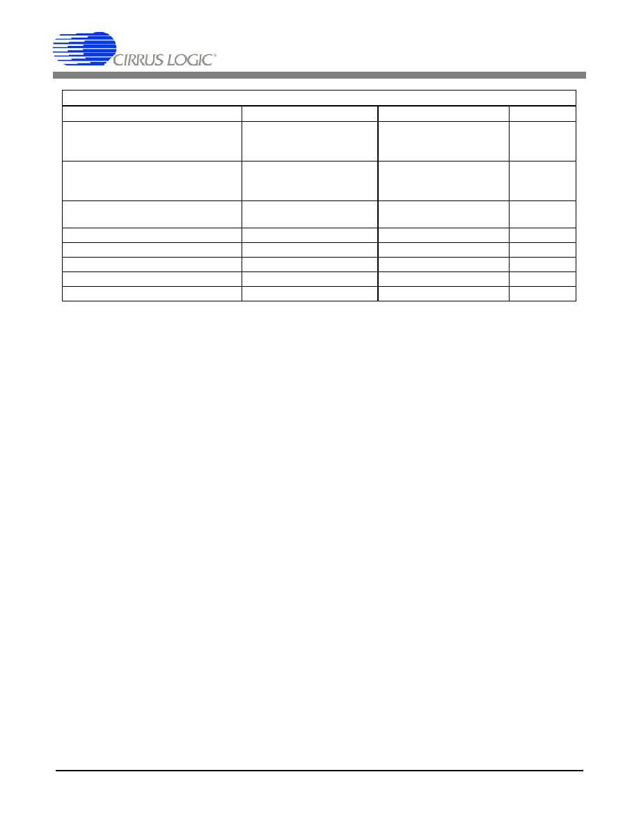
5.2
Analog Inputs
5.2.1 Line Level Inputs
AINx+ and AINx- are the line level differential analog inputs internally biased to VQ, approxi-
mately VA/2. Figure 9 on page 29 shows the full-scale analog input levels. The CS42436 also
accommodates single-ended signals on all inputs, AIN1-AIN6. See "ADC Input Filter" on
page 52 for the recommended input filters.
Hardware Mode
AIN Volume Control and ADC Overflow status are not accessible in Hardware Mode. Single-
ended operation is only supported for ADC3. See section 5.2.2 below.
Software Mode
For single-ended operation on ADC1-ADC3 (AIN1 to AIN6), the ADCx_SINGLE bit in the regis-
ter "ADC Control & DAC De-emphasis (address 05h)" on page 46 must be set appropriately (see
Figure 21 on page 52 for required external components).
The gain/attenuation of the signal can be adjusted for each AINx independently through the
"AINX Volume Control (address 11h-16h)" on page 50. The ADC output data is in 2's comple-
ment binary format. For inputs above positive full scale or below negative full scale, the ADC will
output 7FFFFFH or 800000H, respectively and cause the ADC Overflow bit in the register "Sta-
tus (address 19h) (Read Only)" on page 51 to be set to a `1'.
AIN5 Multiplexer
Selects between AIN5A and
AIN5B when ADC3 in Sin-
gle-Ended Mode
"AIN5_MUX" pin 1
see section
5.2.2
AIN6 Multiplexer
Selects between AIN6A and
AIN6B when ADC3 in Sin-
gle-Ended Mode
"AIN6_MUX" pin 2
see section
5.2.2
DAC Volume Control/Mute/Invert
All DAC Volume = 0 dB, un-
muted, not inverted
-
-
ADC Volume Control
All ADC Volume = 0 dB
-
-
DAC Soft Ramp/Zero Cross
Immediate Change
-
-
ADC Soft Ramp/Zero Cross
Immediate Change
-
-
DAC Auto-Mute
Enabled
-
-
Status Interrupt
N/A
-
-
Hardware Mode Feature Summary
Function
Default Configuration
Hardware Control
Note
Table 2. Hardware Configurable Settings

DS647PP2
29
5.2.2 ADC3 Analog Input
ADC3 accommodates differential as well as single-ended inputs. In Single-Ended mode, an in-
ternal MUX selects from up to 4 single-ended inputs.
Hardware Mode
Single-Ended mode is selected using a pull-up on the ADC_SDOUT/ADC3_SINGLE pin during
startup. Analog input selection is then made via the AINx_MUX pins. See Tables 3-4 below for
ADC3 setup options. Refer to Figure 10 on page 29 for the internal ADC3 analog input topology.
Full-Scale Differential Input Level =
(AINx+) - (AINx-) = 5.6 V
PP
= 1.98 V
RMS
AINx+
AINx-
3.9 V
2.5 V
1.1 V
5.0 V
3.9 V
2.5 V
1.1 V
VA
Figure 9. Full-Scale Input
AIN5
+
-
AIN5_MUX
VQ
AIN6_MUX
VQ
ADC3
Single-Ended Input Filter
Single-Ended Input Filter
Single-Ended Input Filter
Single-Ended Input Filter
Differential
Input Filter
50
49
52
51
ADC3 SINGLE
Differential
Input Filter
AIN5A
AIN5B
AIN5+/-
AIN6+/-
AIN6A
AIN6B
1
0
1
0
1
0
0
1
AIN6
+
-
1
0
0
1
Figure 10. ADC3 Input Topology
30
DS647PP2
Software Mode
Single-Ended mode is selected using the ADC3_SINGLE bit. Analog input selection is then
made via the AINx_MUX bits. See register "ADC Control & DAC De-emphasis (address 05h)"
on page 46 for all bit selections. Refer to Figure 10 on page 29 for the internal ADC3 analog input
topology.
5.2.3 High Pass Filter and DC Offset Calibration
The high pass filter continuously subtracts a measure of the DC offset from the output of the dec-
imation filter. If the high pass filter is disabled during normal operation, the current value of the
DC offset for the corresponding channel is frozen and this DC offset will continue to be subtract-
ed from the conversion result. This feature makes it possible to perform a system DC offset cal-
ibration by:
1) Running the CS42436 with the high pass filter enabled until the filter settles. See the Digital
Filter Characteristics for filter settling time.
2) Disabling the high pass filter and freezing the stored DC offset.
Hardware Mode
The high pass filters for ADC1 and ADC2 are permanently enabled in Hardware Mode. The high
pass filter for ADC3 is enabled by driving the ADC3_HPF (pin 4) high.
Software Mode
The high pass filter for ADC1/ADC2 can be enabled and disabled. The high pass filter for ADC3
can be independently enabled and disabled. The high pass filters are controlled using the
HPF_FREEZE bit in the register "ADC Control & DAC De-emphasis (address 05h)" on page 46.
Configuration Setting
AIN5 Input Selection
ADC_SDOUT
(pin 13)
AIN5_MUX
(pin 1)
47 k
Pull-down
X
Differential Input (pins 50 & 49)
47 k
Pull-up
Low
AIN5A Input (pin 50)
47 k
Pull-up
High
AIN5B Input (pin 49)
Table 3. AIN5 Analog Input Selection
Configuration Setting
AIN6 Input Selection
ADC_SDOUT
(pin 13)
AIN6_MUX
(pin 2)
47 k
Pull-down
X
Differential Input (pins 52 & 51)
47 k
Pull-up
Low
AIN5A Input (pin 52)
47 k
Pull-up
High
AIN5B Input (pin 51)
Table 4. AIN6 Analog Input Selection

DS647PP2
31
5.3
Analog Outputs
5.3.1 Initialization
The initialization and Power-Down sequence flow chart is shown in Figure 11 on page 32. The
CS42436 enters a Power-Down state upon initial power-up. The interpolation & decimation fil-
ters, delta-sigma modulators and control port registers are reset. The internal voltage reference,
multi-bit digital-to-analog and analog-to-digital converters and switched-capacitor low-pass fil-
ters are powered down.
The device will remain in the Power-Down state until the RST pin is brought high. The control
port is accessible once RST is high and the desired register settings can be loaded per the in-
terface descriptions in the "Control Port Description and Timing" on page 37. In hardware mode
operation, the hardware mode pins must be setup before RST is brought high. All features will
default to the hardware mode defaults as listed in Table 2.
Once MCLK is valid, VQ will quickly charge to VA/2, and the internal voltage reference, FILT+,
will begin powering up to normal operation. Power is applied to the D/A converters and switched-
capacitor filters, and the analog outputs are clamped to the quiescent voltage, VQ. Once LRCK is
valid, MCLK occurrences are counted over one LRCK period to determine the MCLK/LRCK fre-
quency ratio. After an approximate 2000 sample period delay, normal operation begins.
5.3.2 Line-level Outputs and Filtering
The CS42436 contains on-chip buffer amplifiers capable of producing line level differential as
well as single-ended outputs on AOUT1-AOUT6. These amplifiers are biased to a quiescent DC
level of approximately VQ.
The delta-sigma conversion process produces high frequency noise beyond the audio pass-
band, most of which is removed by the on-chip analog filters. The remaining out-of-band noise
can be attenuated using an off-chip low pass filter.
See "DAC Output Filter" on page 55 for recommended output filter. The active filter configuration
accounts for the normally differing AC loads on the AOUTx+ and AOUTx- differential output pins.
Also shown is a passive filter configuration which minimizes costs and the number of compo-
nents.
Figure 12 shows the full-scale analog output levels. All outputs are internally biased to VQ, ap-
proximately VA/2.
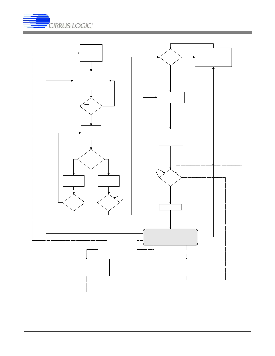
32
DS647PP2
No Power
1. VQ = ?
2. Aout bias = ?
3. No audio signal
generated.
Control Port
Accessed
Control Port
Access Detected?
Valid MCLK
Applied?
Valid MCLK
Applied?
No
PDN bit = '1'b?
Sub-Clocks Applied
1. LRCK valid.
2. SCLK valid.
3. Audio samples
processed.
Valid
MCLK/LRCK
Ratio?
No
Yes
Yes
No
Yes
No
Yes
No
Yes
Yes
No
Normal Operation
1. VQ = VA/2.
2. Aout bias = VA/2.
3. Audio signal generated per register settings.
Analog Output Freeze
1. VQ = VA/2.
2. Aout bias = VA/2 + last audio sample.
3. No audio signal generated.
Analog Output Mute
1. VQ = VA/2.
2. Aout bias = VA/2.
3. No audio signal generated.
ERROR: MCLK/LRCK ratio change
ERROR: MCLK removed
RST = Low
ERROR: Power removed
PDN bit set
to '1'b
Software Mode
Registers setup to
desired settings.
Hardware Mode
H/W pins setup to
desired settings.
RST = Low?
2000 LRCK delay
Power-Up
1. VQ = VA/2.
2. Aout bias = VQ.
Power-Down
1. VQ discharge to 0 V.
2. Aout bias = Hi-Z.
3. No audio signal generated.
4. Control Port Registers retain
settings.
Power-Down (Power Applied)
1. VQ = 0 V.
2. Aout = Hi-Z.
3. No audio signal generated.
4. Control Port Registers reset
to default.
Figure 11. Audio Output Initialization Flow Chart

DS647PP2
33
5.3.3 Digital Volume Control
Hardware Mode
DAC Volume Control and Mute are not accessible in Hardware Mode.
Software Mode
Each DAC's output level is controlled via the Volume Control registers operating over the range
of 0 to -127.5 dB attenuation with 0.5 dB resolution. See "AOUTX Volume Control (addresses
08h-0D)" on page 49. Volume control changes are programmable to ramp in increments of
0.125 dB at the rate controlled by the SZC[1:0] bits in the Digital Volume Control register. See
"Transition Control (address 06h)" on page 47.
Each output can be independently muted via mute control bits in the register "DAC Channel
Mute (address 07h)" on page 49. When enabled, each AOUTx_MUTE bit attenuates the corre-
sponding DAC to its maximum value (-127.5 dB). When the AOUTx_MUTE bit is disabled, the
corresponding DAC returns to the attenuation level set in the Volume Control register. The at-
tenuation is ramped up and down at the rate specified by the SZC[1:0] bits.
5.3.4 De-Emphasis Filter
The CS42436 includes on-chip digital de-emphasis optimized for a sample rate of 44.1 kHz. The
filter response is shown in Figure 13. The de-emphasis feature is included to accommodate au-
dio recordings that utilize 50/15
µ
s pre-emphasis equalization as a means of noise reduction.
AOUTx+
AOUTx-
Full-Scale Differential Output Level =
(AOUTx+) - (AOUTx-) = 6.5 V
PP
= 2.3 V
RMS
4.125 V
2.5 V
0.875 V
5.0 V
4.125 V
2.5 V
0.875 V
VA
Figure 12. Full-Scale Output
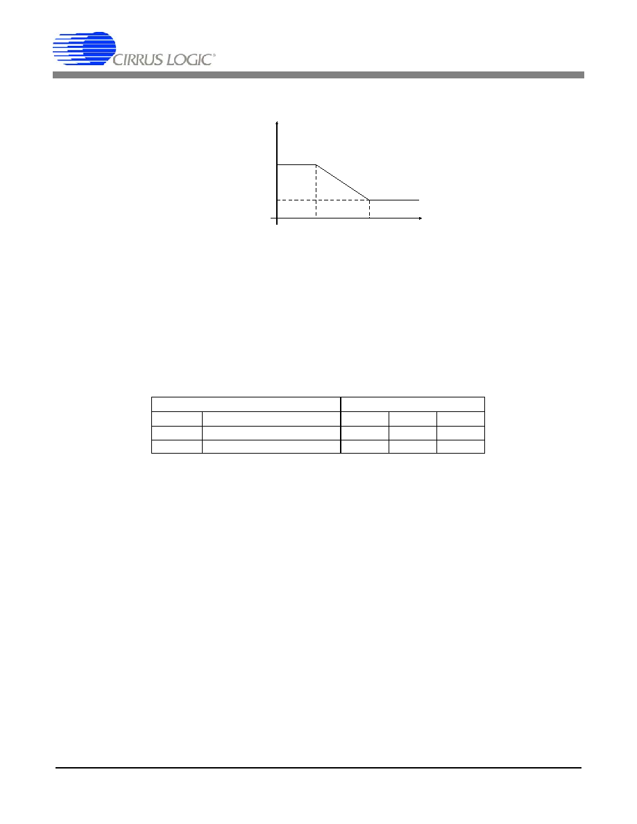
34
DS647PP2
De-emphasis is only available in Single Speed Mode.
Please see "DAC De-Emphasis Control
(DAC_DEM)" on page 46 for de-emphasis control.
5.4
System Clocking
The CODEC serial audio interface ports operate as a slave and accept externally generated clocks.
The CODEC requires external generation of the master clock (MCLK). The frequency of this clock must
be an integer multiple of, and synchronous with, the system sample rate, Fs.
Hardware Mode
The allowable ratios include 256Fs and 512Fs in Single-Speed Mode and 256Fs in Double-Speed Mode.
The frequency of MCLK must be specified using the MFREQ (pin 3). See Table 5 below for the required
frequency range.
Software Mode
The frequency range of MCLK must be specified using the MFREQ bits in register "MCLK Frequency
(MFreq[2:0])" on page 45.
5.5
CODEC Digital Interface
The ADC and DAC serial ports operate as a slave and support the TDM digital interface formats with vary-
ing bit depths from 16 to 32 as shown in Figure 14. Data is clocked out of the ADC on the falling edge of
SCLK and clocked into the DAC on the rising edge.
TDM is the only interface supported in hardware and software mode.
5.5.1 TDM
Data is received most significant bit (MSB) first, on the second rising edge of the SCLK occurring
after an FS rising edge. All data is valid on the rising edge of SCLK. The AIN1 MSB is transmitted
early but is guaranteed valid for a specified time after SCLK rises. All other bits are transmitted
on the falling edge of SCLK. Each time slot is 32 bits wide, with the valid data sample left justified
within the time slot. Valid data lengths are 16, 18, 20, or 24.
SCLK must operate at 256Fs. FS identifies the start of a new frame and is equal to the sample
rate, Fs.
Ratio (xFs)
MFREQ
Description
SSM
DSM
QSM
0
1.5360 MHz to 12.8000 MHz
256
N/A
N/A
1
2.0480 MHz to 25.6000 MHz
512
256
N/A
Table 5. MCLK Frequency Settings
Gain
dB
-10dB
0dB
Frequency
T2 = 15 µs
T1=50 µs
F1
F2
3.183 kHz
10.61 kHz
Figure 13. De-Emphasis Curve

DS647PP2
35
FS is sampled as valid on the rising SCLK edge preceding the most significant bit of the first data
sample and must be held valid for at least 1 SCLK period.
NOTE: The ADC does not meet the timing requirements for proper operation in Quad-Speed
Mode.
5.5.2 I/O Channel Allocation
Digital
Input/Output
Interface
Format
Analog Output/Input Channel Allocation
from/to Digital I/O
DAC_SDIN
TDM
AOUT 1,2,3,4,5,6
ADC_SDOUT
TDM
AIN 1,2,3,4,5,6; (2 additional channels from AUX_SDIN)
Table 6. Serial Audio Interface Channel Allocations
SCLK
FS
256 clks
Bit or Word Wide
AOUT6
LSB
MSB
LSB
MSB
LSB
MSB
LSB
MSB
LSB
MSB
LSB
MSB
DAC_SDIN
AOUT1
AOUT4
AOUT2
AOUT5
AOUT3
32 clks
32 clks
32 clks
32 clks
32 clks
32 clks
-
LSB
MSB
LSB
MSB
-
32 clks
32 clks
MSB
LSB
AIN6
LSB
MSB
LSB
MSB
LSB
MSB
LSB
MSB
LSB
MSB
LSB
MSB
ADC_SDOUT
AIN1
AIN4
AIN2
AIN5
AIN3
32 clks
32 clks
32 clks
32 clks
32 clks
32 clks
AUX2
LSB
MSB
LSB
MSB
AUX1
32 clks
32 clks
MSB
Figure 14. TDM Serial Audio Format
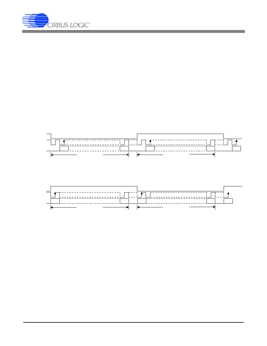
36
DS647PP2
5.6
AUX Port Digital Interface Formats
These serial data lines are used when supporting the TDM Mode of operation with an external ADC or
S/PDIF receiver attached. The AUX serial port operates only as a clock master. The AUX_SCLK will op-
erate at 64xFs, where Fs is equal to the ADC sample rate (FS on the TDM interface). If the AUX_SDIN
signal is not being used, it should be tied to AGND via a pull-down resistor.
Hardware Mode
The AUX port will only operate in the Left Justified digital interface format and supports bit depths ranging
from 16 to 24 bits (see figure 16 on page 36 for timing relationship between AUX_LRCK and AUX_SCLK).
Software Mode
The AUX port will operate in either the Left Justified or I≤S digital interface format with bit depths ranging
from 16 to 24 bits. Settings for the AUX port are made through the register "Miscellaneous Control (ad-
dress 04h)" on page 45.
5.6.1 I≤S
5.6.2 Left Justified
AUX_LRCK
AUX_SCLK
M S B
L S B
M S B
L S B
AUX1
L eft C h a n n el
Rig ht C h a n n el
AUX_SDIN
AUX2
MSB
Figure 15. AUX I≤S Format
AUX_LRCK
AUX_SCLK
M S B
L S B
M S B
L S B
AUX1
L eft C h a n n el
Rig ht C h a n n el
AUX_SDIN
AUX2
MSB
Figure 16. AUX Left Justified Format

DS647PP2
37
5.7
Control Port Description and Timing
The control port is used to access the registers, in software mode, allowing the CS42436 to be configured
for the desired operational modes and formats. The operation of the control port may be completely asyn-
chronous with respect to the audio sample rates. However, to avoid potential interference problems, the
control port pins should remain static if no operation is required.
The control port has 2 modes: SPI and I≤C, with the CS42436 acting as a slave device. SPI mode is se-
lected if there is a high to low transition on the AD0/CS pin, after the RST pin has been brought high. I≤C
mode is selected by connecting the AD0/CS pin through a resistor to VLC or DGND, thereby permanently
selecting the desired AD0 bit address state.
5.7.1 SPI Mode
In SPI mode, CS is the CS42436 chip select signal, CCLK is the control port bit clock (input into
the CS42436 from the microcontroller), CDIN is the input data line from the microcontroller, CD-
OUT is the output data line to the microcontroller. Data is clocked in on the rising edge of CCLK
and out on the falling edge.
Figure 17 shows the operation of the control port in SPI mode. To write to a register, bring CS
low. The first seven bits on CDIN form the chip address and must be 1001111. The eighth bit is
a read/write indicator (R/W), which should be low to write. The next eight bits form the Memory
Address Pointer (MAP), which is set to the address of the register that is to be updated. The next
eight bits are the data which will be placed into the register designated by the MAP. During
writes, the CDOUT output stays in the Hi-Z state. It may be externally pulled high or low with a
47 k
resistor, if desired.
There is a MAP auto increment capability, enabled by the INCR bit in the MAP register. If INCR
is a zero, the MAP will stay constant for successive read or writes. If INCR is set to a 1, the MAP
will autoincrement after each byte is read or written, allowing block reads or writes of successive
registers.
To read a register, the MAP has to be set to the correct address by executing a partial write cycle
which finishes (CS high) immediately after the MAP byte. The MAP auto increment bit (INCR)
may be set or not, as desired. To begin a read, bring CS low, send out the chip address and set
the read/write bit (R/W) high. The next falling edge of CCLK will clock out the MSB of the ad-
M A P
MSB
LSB
DATA
b y te 1
b y te n
R/W
R/W
A D D R E S S
C H IP
ADDRESS
C H IP
C D IN
C C L K
CS
C D O U T
MSB
LSB MSB
LSB
1001111
1001111
MAP = Memory Address Pointer, 8 bits, MSB first
High Impedance
Figure 17. Control Port Timing in SPI Mode

38
DS647PP2
dressed register (CDOUT will leave the high impedance state). If the MAP auto increment bit is
set to 1, the data for successive registers will appear consecutively.
5.7.2 I
2
C Mode
In I≤C mode, SDA is a bidirectional data line. Data is clocked into and out of the part by the clock,
SCL. There is no CS pin. Pins AD0 and AD1 form the two least significant bits of the chip ad-
dress and should be connected through a resistor to VLC or DGND as desired. The state of the
pins is sensed while the CS42436 is being reset.
The signal timings for a read and write cycle are shown in Figure 18 and Figure 19. A Start con-
dition is defined as a falling transition of SDA while the clock is high. A Stop condition is a rising
transition while the clock is high. All other transitions of SDA occur while the clock is low. The
first byte sent to the CS42436 after a Start condition consists of a 7 bit chip address field and a
R/W bit (high for a read, low for a write). The upper 5 bits of the 7-bit address field are fixed at
10010. To communicate with a CS42436, the chip address field, which is the first byte sent to
the CS42436, should match 10010 followed by the settings of the AD1 and AD0. The eighth bit
of the address is the R/W bit. If the operation is a write, the next byte is the Memory Address
Pointer (MAP) which selects the register to be read or written. If the operation is a read, the con-
tents of the register pointed to by the MAP will be output. Setting the auto increment bit in MAP
allows successive reads or writes of consecutive registers. Each byte is separated by an ac-
knowledge bit. The ACK bit is output from the CS42436 after each input byte is read, and is input
to the CS42436 from the microcontroller after each transmitted byte.
Since the read operation can not set the MAP, an aborted write operation is used as a preamble.
As shown in Figure 19, the write operation is aborted after the acknowledge for the MAP byte
by sending a stop condition. The following pseudocode illustrates an aborted write operation fol-
lowed by a read operation.
Send start condition.
Send 10010xx0 (chip address & write operation).
Receive acknowledge bit.
4 5 6 7
24 25
SCL
CHIP ADDRESS (WRITE)
MAP BYTE
DATA
DATA +1
START
ACK
STOP
ACK
ACK
ACK
1 0 0 1 0 AD1 AD0 0
SDA
INCR
6 5 4 3 2 1 0
7 6 1 0
7 6 1 0
7 6 1 0
0 1 2 3
8 9
12
16 17 18 19
10 11
13 14 15
27 28
26
DATA +n
Figure 18. Control Port Timing, I≤C Write
SCL
CHIP ADDRESS (WRITE)
MAP BYTE
DATA
DATA +1
START
ACK
STOP
ACK
ACK
ACK
1 0 0 1 0 AD1 AD0 0
SDA
1 0 0 1 0 AD1 AD0 1
CHIP ADDRESS (READ)
START
INCR
6 5 4 3 2 1 0
7 0
7 0
7 0
NO
16
8 9
12 13 14 15
4 5 6 7
0 1
20 21 22 23 24
26 27 28
2 3
10 11
17 18 19
25
ACK
DATA + n
STOP
Figure 19. Control Port Timing, I≤C Read

DS647PP2
39
Send MAP byte, auto increment off.
Receive acknowledge bit.
Send stop condition, aborting write.
Send start condition.
Send 10010xx1(chip address & read operation).
Receive acknowledge bit.
Receive byte, contents of selected register.
Send acknowledge bit.
Send stop condition.
Setting the auto-increment bit in the MAP allows successive reads or writes of consecutive reg-
isters. Each byte is separated by an acknowledge bit.
5.8
Recommended Power-up Sequence
5.8.1 Hardware Mode
1) Hold RST low until the power supply and hardware control pins are stable. In this state, the
control port is reset to its default settings and VQ will remain low.
2) Bring RST high. The device will initially be in a low power state with VQ low.
3) Start MCLK to the appropriate frequency, as discussed in section 5.4 on page 34.
4) The device will initiate the hardware mode power up sequence. All features will default to the
hardware mode defaults as listed in Table 2 on page 27 according to the hardware mode control
pins. VQ will quick-charge to approximately VA/2 and the analog output bias will clamp to VQ.
5) Apply LRCK, SCLK and SDIN. Following approximately 2000 sample periods, the device is
initialized and ready for normal operation.
NOTE: During the H/W mode power up sequence, there must be no transitions on any of the
hardware control pins.
5.8.2 Software Mode
1) Hold RST low until the power supply is stable. In this state, the control port is reset to its de-
fault settings and VQ will remain low.
2) Bring RST high. The device will initially be in a low power state with VQ low. All features will
default as described in the "Register Quick Reference" on page 41.
3) Perform a write operation to the Power Control register ("Power Control (address 02h)" on
page 44) to set bit 0 to a `1'b. This will place the device in a power down state.
4) Load the desired register settings while keeping the PDN bit set to `1'b.
5) Start MCLK to the appropriate frequency, as discussed in section 5.4 on page 34. The device
will initiate the software mode power up sequence.
6) Set the PDN bit in the power control register to `0'b.
7) Apply LRCK, SCLK and SDIN. Following approximately 2000 sample periods, the device is
initialized and ready for normal operation.
5.9
Reset and Power-up
It is recommended that reset be activated if the analog or digital supplies drop below the recommended
operating condition to prevent power glitch related issues.

40
DS647PP2
The delta-sigma modulators settle in a matter of microseconds after the analog section is powered, either
through the application of power or by setting the RST pin high. However, the voltage reference will take
much longer to reach a final value due to the presence of external capacitance on the FILT+ pin. A time
delay of approximately 400 ms is required after applying power to the device or after exiting a reset state.
During this voltage reference ramp delay, all serial ports and DAC outputs will be automatically muted.
5.10 Power Supply, Grounding, and PCB layout
As with any high resolution converter, the CS42436 requires careful attention to power supply and ground-
ing arrangements if its potential performance is to be realized. Figures 1 to 2 show the recommended
power arrangements, with VA connected to clean supplies. VD, which powers the digital circuitry, may be
run from the system logic supply.
Extensive use of power and ground planes, ground plane fill in unused areas and surface mount decou-
pling capacitors are recommended. Decoupling capacitors should be as near to the pins of the CS42436
as possible. The low value ceramic capacitor should be the nearest to the pin and should be mounted on
the same side of the board as the CS42436 to minimize inductance effects. All signals, especially clocks,
should be kept away from the FILT+, VQ pins in order to avoid unwanted coupling into the modulators.
The FILT+ and VQ decoupling capacitors, particularly the 0.1 µF, must be positioned to minimize the elec-
trical path from FILT+ and AGND. The CDB42438 evaluation board demonstrates the optimum layout and
power supply arrangements.
For optimal heat dissipation from the package, it is recommended that the area directly under the part be
filled with copper and tied to the ground plane. The use of vias connecting the topside ground to the back-
side ground is also recommended.

DS647PP2
41
6 REGISTER QUICK REFERENCE
Software Mode register defaults are as shown. NOTE: The default value in all "Reserved" registers must
be preserved.
Addr Function
7
6
5
4
3
2
1
0
01h
ID
Chip_ID3
Chip_ID2
Chip_ID1
Chip_ID0
Rev_ID3
Rev_ID2
Rev_ID1
Rev_ID0
p 43
default
0
0
0
0
0
0
0
1
02h
Power Con-
trol
PDN_ADC3
PDN_ADC2
PDN_ADC1
Reserved
PDN_DAC3 PDN_DAC2 PDN_DAC1
PDN
p 44
default
0
0
0
0
0
0
0
0
03h
Functional
Mode
Reserved
Reserved
Reserved
Reserved
MFreq2
MFreq1
MFreq0
Reserved
p 45
default
1
1
1
1
0
0
0
0
04h
Misc Control
FREEZE
AUX_DIF
Reserved
Reserved
Reserved
Reserved
Reserved
Reserved
p 45
default
0
0
1
1
0
1
1
0
05h
ADC Control
(w/DAC_DEM)
ADC1-2_HPF
FREEZE
ADC3_HPF
FREEZE
DAC_DEM
ADC1
SINGLE
ADC2
SINGLE
ADC3
SINGLE
AIN5_MUX
AIN6_MUX
p 46
default
0
0
0
0
0
0
0
0
06h
Transition
Control
DAC_SNG
VOL
DAC_SZC1
DAC_SZC0
AMUTE
MUTE
ADC_SP
ADC_SNG
VOL
ADC_SZC1
ADC_SZC0
p 47
default
0
0
0
1
0
0
0
0
07h
Channel
Mute
Reserved
Reserved
AOUT6
MUTE
AOUT5
MUTE
AOUT4
MUTE
AOUT3
MUTE
AOUT2
MUTE
AOUT1
MUTE
p 49
default
0
0
0
0
0
0
0
0
08h
Vol. Control
AOUT1
AOUT1
VOL7
AOUT1
VOL6
AOUT1
VOL5
AOUT1
VOL4
AOUT1
VOL3
AOUT1
VOL2
AOUT1
VOL1
AOUT1
VOL0
p 49
default
0
0
0
0
0
0
0
0
09h
Vol. Control
AOUT2
AOUT2
VOL7
AOUT2
VOL6
AOUT2
VOL5
AOUT2
VOL4
AOUT2
VOL3
AOUT2
VOL2
AOUT2
VOL1
AOUT2
VOL0
p 49
default
0
0
0
0
0
0
0
0
0Ah
Vol. Control
AOUT3
AOUT3
VOL7
AOUT3
VOL6
AOUT3
VOL5
AOUT3
VOL4
AOUT3
VOL3
AOUT3
VOL2
AOUT3
VOL1
AOUT3
VOL0
p 49
default
0
0
0
0
0
0
0
0
0Bh
Vol. Control
AOUT4
AOUT4
VOL7
AOUT4
VOL6
AOUT4
VOL5
AOUT4
VOL4
AOUT4
VOL3
AOUT4
VOL2
AOUT4
VOL1
AOUT4
VOL0
p 49
default
0
0
0
0
0
0
0
0
0Ch
Vol. Control
AOUT5
AOUT5
VOL7
AOUT5
VOL6
AOUT5
VOL5
AOUT5
VOL4
AOUT5
VOL3
AOUT5
VOL2
AOUT5
VOL1
AOUT5
VOL0
p 49
default
0
0
0
0
0
0
0
0
0Dh
Vol. Control
AOUT6
AOUT6
VOL7
AOUT6
VOL6
AOUT6
VOL5
AOUT6
VOL4
AOUT6
VOL3
AOUT6
VOL2
AOUT6
VOL1
AOUT6
VOL0
p 49
default
0
0
0
0
0
0
0
0
0Eh
Reserved
Reserved
Reserved
Reserved
Reserved
Reserved
Reserved
Reserved
Reserved
default
0
0
0
0
0
0
0
0
0Fh
Reserved
Reserved
Reserved
Reserved
Reserved
Reserved
Reserved
Reserved
Reserved
default
0
0
0
0
0
0
0
0
10h
DAC Chan-
nel Invert
Reserved
Reserved
INV_AOUT6 INV_AOUT5 INV_AOUT4 INV_AOUT3 INV_AOUT2
INV_AOUT1
p 50
default
0
0
0
0
0
0
0
0
42
DS647PP2
11h
Vol. Control
AIN1
AIN1
VOL7
AIN1
VOL6
AIN1
VOL5
AIN1
VOL4
AIN1
VOL3
AIN1
VOL2
AIN1
VOL1
AIN1
VOL0
p 49
default
0
0
0
0
0
0
0
0
12h
Vol. Control
AIN2
AIN2
VOL7
AIN2
VOL6
AIN2
VOL5
AIN2
VOL4
AIN2
VOL3
AIN2
VOL2
AIN2
VOL1
AIN2
VOL0
p 50
default
0
0
0
0
0
0
0
0
13h
Vol. Control
AIN3
AIN3
VOL7
AIN3
VOL6
AIN3
VOL5
AIN3
VOL4
AIN3
VOL3
AIN3
VOL2
AIN3
VOL1
AIN3
VOL0
p 49
default
0
0
0
0
0
0
0
0
14h
Vol. Control
AIN4
AIN4
VOL7
AIN4
VOL6
AIN4
VOL5
AIN4
VOL4
AIN4
VOL3
AIN4
VOL2
AIN4
VOL1
AIN4
VOL0
p 50
default
0
0
0
0
0
0
0
0
15h
Vol. Control
AIN5
AIN5
VOL7
AIN5
VOL6
AIN5
VOL5
AIN5
VOL4
AIN5
VOL3
AIN5
VOL2
AIN5
VOL1
AIN5
VOL0
p 49
default
0
0
0
0
0
0
0
0
16h
Vol. Control
AIN6
AIN6
VOL7
AIN6
VOL6
AIN6
VOL5
AIN6
VOL4
AIN6
VOL3
AIN6
VOL2
AIN6
VOL1
AIN6
VOL0
p 50
default
0
0
0
0
0
0
0
0
17h
ADC Chan-
nel Invert
Reserved
Reserved
INV_A6
INV_A5
INV_A4
INV_A3
INV_A2
INV_A1
p 50
default
0
0
0
0
0
0
0
0
18h
Reserved
Reserved
Reserved
Reserved
Reserved
Reserved
Reserved
Reserved
Reserved
default
0
0
0
0
0
0
0
0
19h
Status
Reserved
Reserved
Reserved
Reserved
CLK
Error
ADC3
OVFL
ADC2
OVFL
ADC1
OVFL
p 51
default
0
0
0
X
X
X
X
X
1Ah
Status Mask
Reserved
Reserved
Reserved
Reserved
CLK
Error_M
ADC3
OVFL_M
ADC2
OVFL_M
ADC1
OVFL_M
p 51
default
0
0
0
0
0
0
0
0
Addr Function
7
6
5
4
3
2
1
0
DS647PP2
43
7 REGISTER DESCRIPTION
All registers are read/write except for the I.D. and Revision Register and Interrupt Status Register which
are read only. See the following bit definition tables for bit assignment information. The default state of
each bit after a power-up sequence or reset is listed in each bit description.
7.1
MEMORY ADDRESS POINTER (MAP)
Not a register
7.1.1
INCREMENT(INCR)
Default = 1
Function:
Memory address pointer auto increment control
0 - MAP is not incremented automatically.
1 - Internal MAP is automatically incremented after each read or write.
7.1.2
MEMORY ADDRESS POINTER (MAP[6:0])
Default = 0000001
Function:
Memory address pointer (MAP). Sets the register address that will be read or written by the control
port.
7.2
CHIP I.D. AND REVISION REGISTER (ADDRESS 01H) (READ ONLY)
7.2.1
CHIP I.D. (CHIP_ID[3:0])
Default = 0000
Function:
I.D. code for the CS42436. Permanently set to 0000.
7.2.2
CHIP REVISION (REV_ID[3:0])
Default = 0001
Function:
CS42436 revision level. Revision A is coded as 0001.
7
6
5
4
3
2
1
0
INCR
MAP6
MAP5
MAP4
MAP3
MAP2
MAP1
MAP0
7
6
5
4
3
2
1
0
Chip_ID3
Chip_ID2
Chip_ID1
Chip_ID0
Rev_ID3
Rev_ID2
Rev_ID1
Rev_ID0

44
DS647PP2
7.3
POWER CONTROL (ADDRESS 02H)
7.3.1
POWER DOWN ADC PAIRS(PDN_ADCX)
Default = 0
0 - Disable
1 - Enable
Function:
When enabled, the respective ADC channel pair (ADC1 - AIN1/AIN2; ADC2 - AIN3/AIN4; and ADC3
- AIN5/AIN6) will remain in a reset state.
7.3.2
POWER DOWN DAC PAIRS (PDN_DACX)
Default = 0
0 - Disable
1 - Enable
Function:
When enabled, the respective DAC channel pair (DAC1 - AOUT1/AOUT2; DAC2 - AOUT3/AOUT4;
and DAC3 - AOUT5/AOUT6) will remain in a reset state. It is advised that any change of these bits
be made while the DACs are muted or the power down bit (PDN) is enabled to eliminate the possibility
of audible artifacts.
7.3.3
POWER DOWN (PDN)
Default = 0
0 - Disable
1 - Enable
Function:
The entire device will enter a low-power state when this function is enabled. The contents of the con-
trol registers are retained in this mode.
7
6
5
4
3
2
1
0
PDN_ADC3
PDN_ADC2
PDN_ADC1
Reserved
PDN_DAC3
PDN_DAC2
PDN_DAC1
PDN
DS647PP2
45
7.4
FUNCTIONAL MODE (ADDRESS 03H)
7.4.1
MCLK FREQUENCY (MFREQ[2:0])
Default = 000
Function:
Sets the appropriate frequency for the supplied MCLK. For TDM operation, SCLK must equal 256Fs.
MCLK can be equal to or greater than SCLK.
7.5
MISCELLANEOUS CONTROL (ADDRESS 04H)
7.5.1
FREEZE CONTROLS (FREEZE)
Default = 0
Function:
This function will freeze the previous settings of, and allow modifications to be made to the channel
mutes, the DAC and ADC Volume Control/Channel Invert registers without the changes taking effect
until the FREEZE is disabled. To have multiple changes in these control port registers take effect si-
multaneously, enable the FREEZE bit, make all register changes, then disable the FREEZE bit.
7.5.2
AUXILIARY DIGITAL INTERFACE FORMAT (AUX_DIF)
Default = 0
0 - Left Justified
1 - I≤S
Function:
This bit selects the digital interface format used for the AUX Serial Port. The required relationship be-
tween the Left/Right clock, serial clock and serial data is defined by the Digital Interface Format and
the options are detailed in Figures 15-16.
7
6
5
4
3
2
1
0
Reserved
Reserved
Reserved
Reserved
MFreq2
MFreq1
MFreq0
Reserved
Ratio (xFs)
MFreq2
MFreq1
MFreq0
Description
SSM
DSM
QSM
0
0
0
1.0290 MHz to 12.8000 MHz
256
N/A
N/A
0
0
1
1.5360 MHz to 19.2000 MHz
384
N/A
N/A
0
1
0
2.0480 MHz to 25.6000 MHz
512
256
N/A
0
1
1
3.0720 MHz to 38.4000 MHz
768
384
N/A
1
X
X
4.0960 MHz to 51.2000 MHz
1024
512
256
Table 7. MCLK Frequency Settings
7
6
5
4
3
2
1
0
FREEZE
AUX_DIF
Reserved
Reserved
Reserved
Reserved
Reserved
Reserved

46
DS647PP2
7.6
ADC CONTROL & DAC DE-EMPHASIS (ADDRESS 05H)
7.6.1
ADC1-2 HIGH PASS FILTER FREEZE (ADC1-2_HPF FREEZE)
Default = 0
Function:
When this bit is set, the internal high-pass filter will be disabled for ADC1 and ADC2.The current DC
offset value will be frozen and continue to be subtracted from the conversion result. See "ADC Digital
Filter Characteristics" on page 16.
7.6.2
ADC3 HIGH PASS FILTER FREEZE (ADC3_HPF FREEZE)
Default = 0
Function:
When this bit is set, the internal high-pass filter will be disabled for ADC3.The current DC offset value
will be frozen and continue to be subtracted from the conversion result. See "ADC Digital Filter Char-
acteristics" on page 16.
7.6.3
DAC DE-EMPHASIS CONTROL (DAC_DEM)
Default = 0
0 - No De-Emphasis
1 - De-Emphasis Enabled (Auto-Detect Fs)
Function:
Enables the digital filter to maintain the standard 15
µ
s/50
µ
s digital de-emphasis filter response at the
auto-detected sample rate of either 32, 44.1, or 48 kHz. De-emphasis will not be enabled, regardless
of this register setting, at any other sample rate.
7.6.4
ADC1 SINGLE-ENDED MODE (ADC1 SINGLE)
Default = 0
0 - Disabled; Differential input to ADC1
1 - Enabled; Single-Ended input to ADC1
Function:
When enabled, this bit allows the user to apply a single-ended input to the positive terminal of ADC1.
+6 dB digital gain is automatically applied to the serial audio data of ADC1. The negative leg must be
driven to the common mode of the ADC. See Figure 21 on page 52 for a graphical description.
7.6.5
ADC2 SINGLE-ENDED MODE (ADC2 SINGLE)
Default = 0
0 - Disabled; Differential input to ADC2
1 - Enabled; Single-Ended input to ADC2
7
6
5
4
3
2
1
0
ADC1-2_HPF
FREEZE
ADC3_HPF
FREEZE
DAC_DEM
ADC1
SINGLE
ADC2
SINGLE
ADC3
SINGLE
AIN5_MUX
AIN6_MUX

DS647PP2
47
Function:
When enabled, this bit allows the user to apply a single-ended input to the positive terminal of ADC2.
+6 dB digital gain is automatically applied to the serial audio data of ADC2. The negative leg must be
driven to the common mode of the ADC. See Figure 21 on page 52 for a graphical description.
7.6.6
ADC3 SINGLE-ENDED MODE (ADC3 SINGLE)
Default = 0
0 - Disabled; Differential input to ADC
1 - Enabled; Single-Ended input to ADC
Function:
When disabled, this bit removes the 4:2 multiplexer from the signal path of ADC3 allowing a differen-
tial input. When enabled, this bit allows the user to choose between 4 single-ended inputs to ADC3,
using the AIN5_MUX and AIN6_MUX bits. See Figure 10 on page 29 and Figure 21 on page 52 for
graphical descriptions.
7.6.7
ANALOG INPUT CH. 5 MULTIPLEXER (AIN5_MUX)
Default = 0
0 - Single-Ended Input AIN5A
1 - Single-Ended Input AIN5B
Function:
ADC3 can accept single-ended input signals when the ADC3 SINGLE bit is enabled. The AIN5_MUX
bit selects between two input channels (AIN5A or AIN5B) to be sent to ADC3 in single-ended mode.
This bit is ignored when the ADC3_SINGLE bit is disabled. See Figure 10 on page 29 for a graphical
description.
7.6.8
ANALOG INPUT CH. 6 MULTIPLEXER (AIN6_MUX)
Default = 0
0 - Single-Ended Input AIN6A
1 - Single-Ended Input AIN6B
Function:
ADC3 can accept a single-ended input signal when the ADC3 SINGLE bit is enabled. The AIN6_MUX
bit selects between two input channels (AIN6A or AIN6B) to be sent to ADC3 in single-ended mode.
This bit is ignored when the ADC3_SINGLE bit is disabled. See Figure 10 on page 29 for a graphical
description.
7.7
TRANSITION CONTROL (ADDRESS 06H)
7.7.1
SINGLE VOLUME CONTROL (DAC_SNGVOL, ADC_SNGVOL)
Default = 0
7
6
5
4
3
2
1
0
DAC_SNGVOL
DAC_SZC1
DAC_SZC0
AMUTE
MUTE ADC_SP ADC_SNGVOL
ADC_SZC1
ADC_SZC0
48
DS647PP2
Function:
The individual channel volume levels are independently controlled by their respective Volume Control
registers when this function is disabled. When enabled, the volume on all channels is determined by
the AOUT1 and AIN1 Volume Control register and the other Volume Control registers are ignored.
7.7.2
SOFT RAMP AND ZERO CROSS CONTROL (ADC_SZC[1:0], DAC_SZC[1:0])
Default = 00
00 - Immediate Change
01 - Zero Cross
10 - Soft Ramp
11 - Soft Ramp on Zero Crossings
Function:
Immediate Change
When Immediate Change is selected all volume level changes will take effect immediately in one step.
Zero Cross
Zero Cross Enable dictates that signal level changes, either by gain changes, attenuation changes or
muting, will occur on a signal zero crossing to minimize audible artifacts. The requested level change
will occur after a timeout period between 512 and 1024 sample periods (10.7 ms to 21.3 ms at 48 kHz
sample rate) if the signal does not encounter a zero crossing. The zero cross function is independent-
ly monitored and implemented for each channel.
Soft Ramp
Soft Ramp allows level changes, either by gain changes, attenuation changes or muting, to be imple-
mented by incrementally ramping, in 1/8 dB steps, from the current level to the new level at a rate of
1 dB per 8 left/right clock periods.
Soft Ramp on Zero Crossing
Soft Ramp and Zero Cross Enable dictates that signal level changes, either by gain changes, atten-
uation changes or muting, will occur in 1/8 dB steps and be implemented on a signal zero crossing.
The 1/8 dB level change will occur after a timeout period between 512 and 1024 sample periods (10.7
ms to 21.3 ms at 48 kHz sample rate) if the signal does not encounter a zero crossing. The zero cross
function is independently monitored and implemented for each channel.
7.7.3
AUTO-MUTE (AMUTE)
Default = 1
0 - Disabled
1 - Enabled
Function:
The Digital-to-Analog converters of the CS42436 will mute the output following the reception of 8192
consecutive audio samples of static 0 or -1. A single sample of non-static data will release the mute.
Detection and muting is done independently for each channel. The quiescent voltage on the output
will be retained during the mute period. The muting function is affected, similar to volume control
changes, by the Soft and Zero Cross bits (SZC[1:0]).
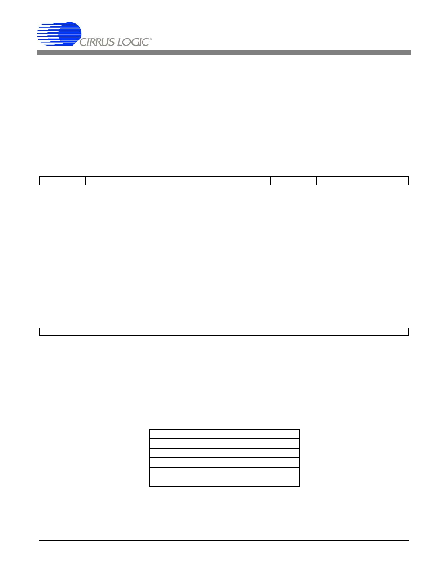
DS647PP2
49
7.7.4
MUTE ADC SERIAL PORT (MUTE ADC_SP)
Default = 0
0 - Disabled
1 - Enabled
Function:
When enabled, the ADC Serial Port will be muted.
7.8
DAC CHANNEL MUTE (ADDRESS 07H)
7.8.1
INDEPENDENT CHANNEL MUTE (AOUTX_MUTE)
Default = 0
0 - Disabled
1 - Enabled
Function:
The respective Digital-to-Analog converter outputs of the CS42436 will mute when enabled. The qui-
escent voltage on the outputs will be retained. The muting function is affected by the DAC Soft and
Zero Cross bits (DAC_SZC[1:0]).
7.9
AOUTX VOLUME CONTROL (ADDRESSES 08H-0D)
7.9.1
VOLUME CONTROL (AOUTX_VOL[7:0])
Default = 00h
Function:
The AOUTx Volume Control registers allow independent setting of the signal levels in 0.5 dB incre-
ments from 0 dB to -127.5 dB. Volume settings are decoded as shown in Table 8. The volume chang-
es are implemented as dictated by the Soft and Zero Cross bits (DAC_SZC[1:0]). All volume settings
less than -127.5 dB are equivalent to enabling the AOUTx_MUTE bit for the given channel.
7
6
5
4
3
2
1
0
Reserved
Reserved
AOUT6_MUTE
AOUT5_MUTE
AOUT4_MUTE
AOUT3_MUTE
AOUT2_MUTE
AOUT1_MUTE
7
6
5
4
3
2
1
0
AOUTx_VOL7
AOUTx_VOL6
AOUTx_VOL5
AOUTx_VOL4
AOUTx_VOL3
AOUTx_VOL2
AOUTx_VOL1
AOUTx_VOL0
Binary Code
Volume Setting
00000000
0 dB
00101000
-20 dB
01010000
-40 dB
01111000
-60 dB
10110100
-90 dB
Table 8. Example AOUT Volume Settings

50
DS647PP2
7.10 DAC CHANNEL INVERT (ADDRESS 10H)
7.10.1 INVERT SIGNAL POLARITY (INV_AOUTX)
Default = 0
0 - Disabled
1 - Enabled
Function:
When enabled, these bits will invert the signal polarity of their respective channels.
7.11 AINX VOLUME CONTROL (ADDRESS 11H-16H)
7.11.1 AINX VOLUME CONTROL (AINX_VOL[7:0])
Default = 00h
Function:
The level of AIN1 - AIN6 can be adjusted in 0.5 dB increments as dictated by the ADC Soft and Zero
Cross bits (ADC_SZC[1:0]) from +24 to -64 dB. Levels are decoded in two's complement, as shown
in Table 9.
7.12 ADC CHANNEL INVERT (ADDRESS 17H)
7.12.1 INVERT SIGNAL POLARITY (INV_AINX)
Default = 0
0 - Disabled
1 - Enabled
7
6
5
4
3
2
1
0
Reserved
Reserved
INV_AOUT6
INV_AOUT5
INV_AOUT4
INV_AOUT3
INV_AOUT2
INV_AOUT1
7
6
5
4
3
2
1
0
AINx_VOL7
AINx_VOL6
AINx_VOL5
AINx_VOL4
AINx_VOL3
AINx_VOL2
AINx_VOL1
AINx_VOL0
Binary Code
Volume Setting
0111 1111
+24 dB
∑∑∑
∑∑∑
0011 0000
+24 dB
∑∑∑
∑∑∑
0000 0000
0 dB
1111 1111
-0.5 dB
1111 1110
-1 dB
∑∑∑
∑∑∑
1000 0000
-64 dB
Table 9. Example AIN Volume Settings
7
6
5
4
3
2
1
0
Reserved
Reserved
INV_AIN6
INV_AIN5
INV_AIN4
INV_AIN3
INV_AIN2
INV_AIN1
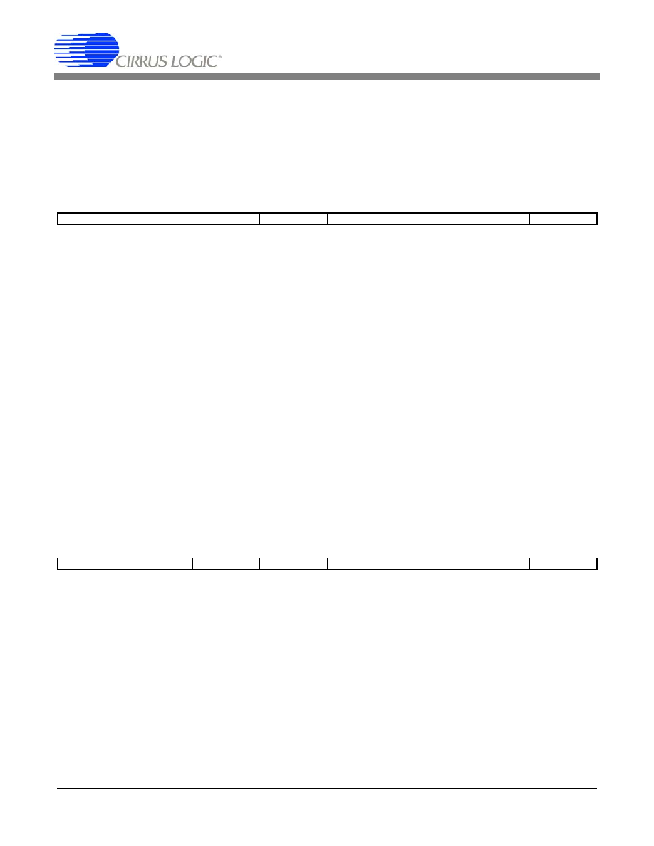
DS647PP2
51
Function:
When enabled, these bits will invert the signal polarity of their respective channels.
7.13 STATUS (ADDRESS 19H) (READ ONLY)
For all bits in this register, a "1" means the associated error condition has occurred at least once since the register
was last read. A"0" means the associated error condition has NOT occurred since the last reading of the register.
Reading the register resets all bits to 0. Status bits that are masked off in the associated mask register will always
be "0" in this register.
7.13.1 CLOCK ERROR (CLK ERROR)
Default = x
Function:
Indicates an invalid MCLK to FS ratio. This status flag is set to "Level Active Mode" and becomes ac-
tive during the error condition. See "System Clocking" on page 34 for valid clock ratios.
7.13.2 ADC OVERFLOW (ADCX_OVFL)
Default = x
Function:
Indicates that there is an over-range condition anywhere in the CS42436 ADC signal path of each of
the associated ADC's.
7.14 STATUS MASK (ADDRESS 1AH)
Default = 0000
Function:
The bits of this register serve as a mask for the error sources found in the register "Status (address
19h) (Read Only)" on page 51. If a mask bit is set to 1, the error is unmasked, meaning that its occur-
rence will affect the status register. If a mask bit is set to 0, the error is masked, meaning that its oc-
currence will not affect status register. The bit positions align with the corresponding bits in the Status
register.
7
6
5
4
3
2
1
0
Reserved
Reserved
Reserved
Reserved
CLK Error
ADC3_OVFL
ADC2_OVFL
ADC1_OVFL
7
6
5
4
3
2
1
0
Reserved
Reserved
Reserved
Reserved
CLK Error_M
ADC3_OVFL_M ADC2_OVFL_M ADC1_OVFL_M

52
DS647PP2
8 APPENDIX A: EXTERNAL FILTERS
8.1
ADC Input Filter
The analog modulator samples the input at 6.144 MHz (internal MCLK=12.288 MHz). The digital filter will
reject signals within the stopband of the filter. However, there is no rejection for input signals which are
multiples of the digital passband frequency (n
◊
6.144 MHz), where n=0,1,2,...
Refer to Figures 20 and 21
for a recommended analog input filter that will attenuate any noise energy at 6.144 MHz, in addition to
providing the optimum source impedance for the modulators. Refer to Figures 22 and 23 for low cost, low
component count passive input filters. The use of capacitors which have a large voltage coefficient (such
as general-purpose ceramics) must be avoided since these can degrade signal linearity.
VA
+
+
-
-
4.7
µ
F
100 k
10 k
100 k
100 k
0.1
µ
F
100
µ
F
470 pF
470 pF
C0G
C0G
634
634
634
91
91
2700 pF
C0G
332
AINx+
AINx-
ADC1-3
Figure 20. Single to Differential Active Input Filter
-
+
470 pF
C0G
634
91
2700 pF
C0G
4.7
µ
F
100 k
100 k
100 k
VA
4.7
µ
F
AIN1+,2+,3+,4+
AIN1-,2-,3-,4-
ADC1-2
ADC3
-
+
470 pF
C0G
634
91
2700 pF
C0G
4.7
µ
F
100 k
100 k
100 k
VA
AIN5A,6A
-
+
470 pF
C0G
634
91
2700 pF
C0G
4.7
µ
F
100 k
100 k
100 k
VA
AIN5B,6B
Figure 21. Single-Ended Active Input Filter
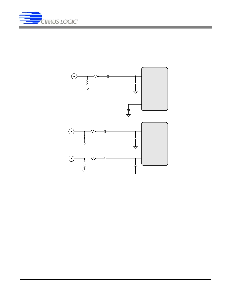
DS647PP2
53
8.1.1 Passive Input Filter
The passive filter implementation shown in Figure 22 will attenuate any noise energy at
6.144 MHz but will not provide optimum source impedance for the ADC modulators. Full analog
performance will therefore not be realized using a passive filter. Figure 22 illustrates the unity
gain, passive input filter solution. In this topology the distortion performance is affected, but the
dynamic range performance is not limited.
8.1.2 Passive Input Filter w/Attenuation
Some applications may require signal attenuation prior to the ADC. The full-scale input voltage
will scale with the analog power supply voltage. For VA = 5.0 V, the full-scale input voltage is
approximately 2.8 Vpp, or 1 Vrms (most consumer audio line-level outputs range from 1.5 to
2 Vrms).
Figure 23 shows a passive input filter with 6 dB of signal attenuation. Due to the relatively high
input impedance on the analog inputs, the full distortion performance cannot be realized. Also,
the resistor divider circuit will determine the input impedance into the input filter. In the circuit
shown in Figure 23, the input impedance is approximately 5 k
.
By doubling the resistor values,
the input impedance will increase to 10 k
.
However, in this case the distortion performance will
drop due to the increase in series resistance on the analog inputs.
2700 pF
C0G
10
µ
F
100 k
150
AIN1+,2+,3+,4+
AIN1-,2-,3-,4-
ADC1-2
4.7
µ
F
AIN5A,6A
AIN5B,6B
ADC3
2700 pF
C0G
10
µ
F
100 k
150
2700 pF
C0G
10
µ
F
100 k
150
Figure 22. Passive Input Filter
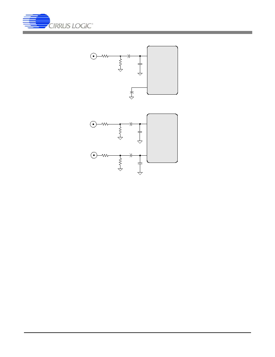
54
DS647PP2
2700 pF
C0G
10
µ
F
2.5 k
AIN1+,2+,3+,4+
AIN1-,2-,3-,4-
ADC1-2
4.7
µ
F
2700 pF
C0G
10
µ
F
2.5 k
AIN5A,6A
AIN5B,6B
ADC3
2700 pF
C0G
10
µ
F
2.5 k
2.5 k
2.5 k
2.5 k
Figure 23. Passive Input Filter w/Attenuation

DS647PP2
55
8.2
DAC Output Filter
The CS42436 is a linear phase design and does not include phase or amplitude compensation for an ex-
ternal filter. Therefore, the DAC system phase and amplitude response will be dependent on the external
analog circuitry. Shown below is the recommended active and passive output filters.
AOUTx +
AOUTx -
-
+
390 pF
C0G
562
22
µ
F
4.75 k
1800 pF
C0G
887
2.94 k
5.49 k
1.65 k
1.87 k
22
µ
F
1200 pF
C0G
5600 pF
C0G
47.5 k
DAC1-3
Figure 24. Active Analog Output Filter
AOUTx+
3.3 µF
C
560
+
10 k
R ext
R
ext
+ 560
C =
4
F
S
R
ext
560
DAC1-3
Figure 25. Passive Analog Output Filter
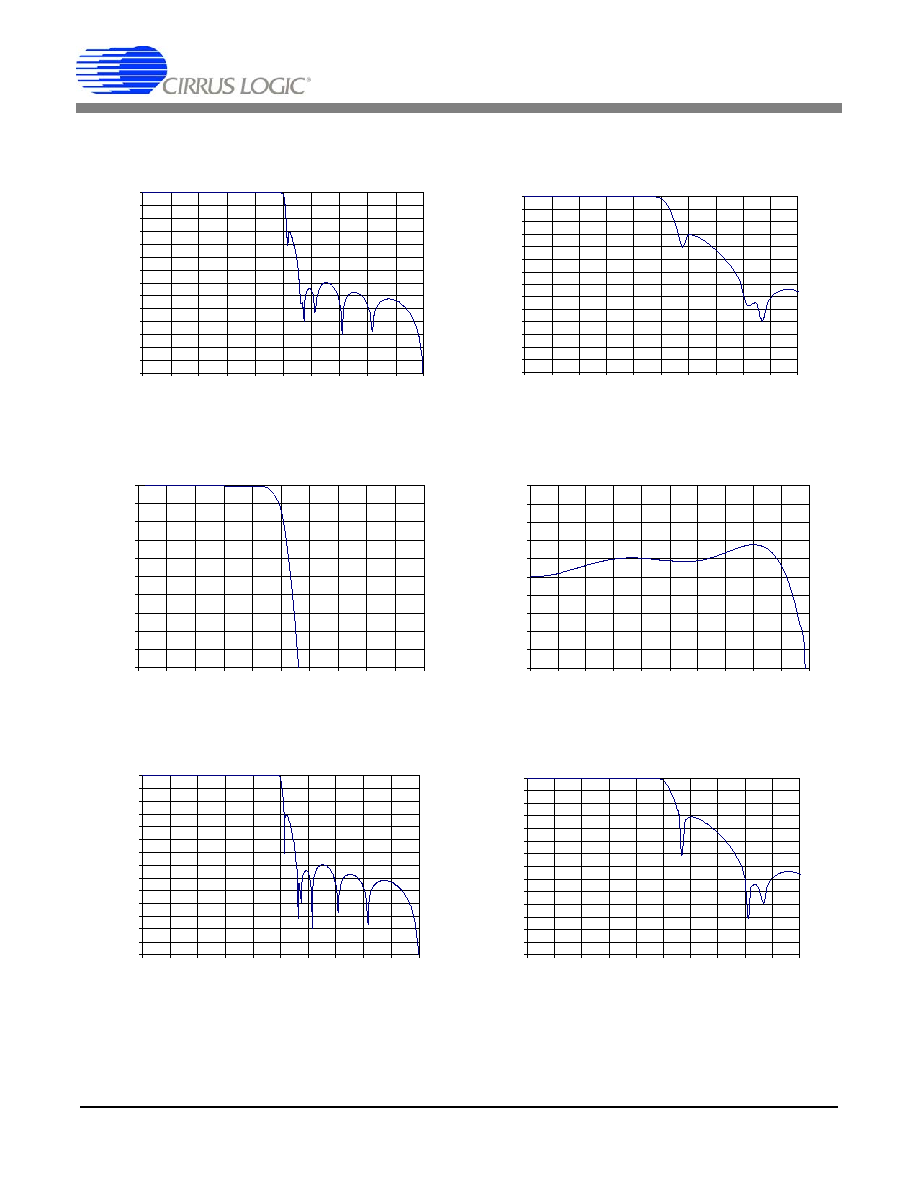
56
DS647PP2
9 APPENDIX B: ADC FILTER PLOTS
-140
-130
-120
-110
-100
-90
-80
-70
-60
-50
-40
-30
-20
-10
0
0.0
0.1
0.2
0.3
0.4
0.5
0.6
0.7
0.8
0.9
1.0
Frequency (normalized to Fs)
Am
p
l
i
t
u
d
e (
d
B
)
-140
-130
-120
-110
-100
-90
-80
-70
-60
-50
-40
-30
-20
-10
0
0.40
0.42
0.44
0.46
0.48
0.50
0.52
0.54
0.56
0.58
0.60
Frequency (normalized to Fs)
A
m
pl
i
t
ud
e
(
d
B
)
Figure 26. SSM Stopband Rejection
Figure 27. SSM Transition Band
-10
-9
-8
-7
-6
-5
-4
-3
-2
-1
0
0.45
0.46
0.47
0.48
0.49
0.5
0.51
0.52
0.53
0.54
0.55
Frequency (normalized to Fs)
Am
p
l
i
t
ud
e (
d
B
)
-0.10
-0.08
-0.06
-0.04
-0.02
0.00
0.02
0.04
0.06
0.08
0.10
0
0.05
0.1
0.15
0.2
0.25
0.3
0.35
0.4
0.45
0.5
Frequency (normalized to Fs)
A
m
pl
i
t
ud
e (
d
B
)
Figure 28. SSM Transition Band (Detail)
Figure 29. SSM Passband Ripple
-140
-130
-120
-110
-100
-90
-80
-70
-60
-50
-40
-30
-20
-10
0
0.0
0.1
0.2
0.3
0.4
0.5
0.6
0.7
0.8
0.9
1.0
Frequency (normalized to Fs)
Am
p
l
i
t
u
d
e
(
d
B
)
-140
-130
-120
-110
-100
-90
-80
-70
-60
-50
-40
-30
-20
-10
0
0.40
0.42
0.44
0.46
0.48
0.50
0.52
0.54
0.56
0.58
0.60
Frequency (normalized to Fs)
Am
p
l
i
t
u
d
e
(d
B)
Figure 30. DSM Stopband Rejection
Figure 31. DSM Transition Band

DS647PP2
57
`
-0.10
-0 .0 8
-0 .0 6
-0 .0 4
-0 .0 2
0 .0 0
0 .0 2
0 .0 4
0 .0 6
0 .0 8
0.10
0.00 0.05
0 .10
0.15
0 .2 0 0 .2 5 0 .3 0 0 .3 5 0.40 0.45 0.50
Fre que ncy (norm alize d to Fs )
A
m
p
l
i
t
ude
(
d
B
)
-10
-9
-8
-7
-6
-5
-4
-3
-2
-1
0
0.46
0.47
0.48
0.49
0.50
0.51
0.52
Frequency (normalized to Fs)
A
m
p
lit
u
d
e
(
d
B
)
Figure 32. DSM Transition Band (Detail)
Figure 33. DSM Passband Ripple
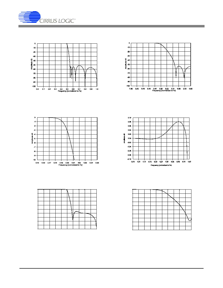
58
DS647PP2
10 APPENDIX C: DAC FILTER PLOTS
Figure 34. SSM Stopband Rejection
Figure 35. SSM Transition Band
Figure 36. SSM Transition Band (detail)
Figure 37. SSM Passband Ripple
-100
-90
-80
-70
-60
-50
-40
-30
-20
-10
0
0.0
0.1
0.2
0.3
0.4
0.5
0.6
0.7
0.8
0.9
1.0
Frequency (normalized to Fs)
A
m
pl
it
ude
dB
-100
-90
-80
-70
-60
-50
-40
-30
-20
-10
0
0.40
0.42
0.44
0.46
0.48
0.50
0.52
0.54
0.56
0.58
0.60
Frequency (normalized to Fs)
A
m
pl
i
t
u
d
e d
B
Figure 38. DSM Stopband Rejection
Figure 39. DSM Transition Band

DS647PP2
59
-10
-9
-8
-7
-6
-5
-4
-3
-2
-1
0
0.45
0.46
0.47
0.48
0.49
0.50
0.51
0.52
0.53
0.54
0.55
Frequency (normalized to Fs)
Am
pl
i
t
ude dB
-0.30
-0.25
-0.20
-0.15
-0.10
-0.05
0.00
0.05
0.10
0.15
0.20
0.25
0.30
0.00
0.05
0.10
0.15
0.20
0.25
0.30
0.35
0.40
0.45
0.50
Frequency (normalized to Fs)
A
m
pl
i
t
u
d
e d
B
Figure 40. DSM Transition Band (detail)
Figure 41. DSM Passband Ripple
0.35
0.4
0.45
0.5
0.55
0.6
0.65
0.7
0.75
-60
-50
-40
-30
-20
-10
0
Amplitude (dB)
Frequency(normalized to Fs)
Figure 42. QSM Stopband Rejection
Figure 43. QSM Transition Band
0
0.1
0.2
0.3
0.4
0.5
0.6
0.7
0.8
0.9
1
-100
-90
-80
-70
-60
-50
-40
-30
-20
-10
0
Amplitude (dB)
Frequency(normalized to Fs)
0.4
0.45
0.5
0.55
0.6
0.65
0.7
-50
-45
-40
-35
-30
-25
-20
-15
-10
-5
0
Amplitude (dB)
Frequency(normalized to Fs)
0.05
0.1
0.15
0.2
0.25
0.3
0.35
0.4
0.45
-0.2
-0.15
-0.1
-0.05
0
0.05
0.1
0.15
0.2
Amplitude (dB)
Frequency(normalized to Fs)
Figure 44. QSM Transition Band (detail)
Figure 45. QSM Passband Ripple

60
DS647PP2
11 PARAMETER DEFINITIONS
Dynamic Range
The ratio of the rms value of the signal to the rms sum of all other spectral components over the specified
bandwidth. Dynamic Range is a signal-to-noise ratio measurement over the specified band width made
with a -60 dBFS signal. 60 dB is added to resulting measurement to refer the measurement to full-scale.
This technique ensures that the distortion components are below the noise level and do not affect the
measurement. This measurement technique has been accepted by the Audio Engineering Society,
AES17-1991, and the Electronic Industries Association of Japan, EIAJ CP-307. Expressed in decibels.
Total Harmonic Distortion + Noise
The ratio of the rms value of the signal to the rms sum of all other spectral components over the specified
band width (typically 10 Hz to 20 kHz), including distortion components. Expressed in decibels. Measured
at -1 and -20 dBFS as suggested in AES17-1991 Annex A.
Frequency Response
A measure of the amplitude response variation from 10 Hz to 20 kHz relative to the amplitude response
at 1 kHz. Units in decibels.
Interchannel Isolation
A measure of crosstalk between the left and right channel pairs. Measured for each channel at the con-
verter's output with no signal to the input under test and a full-scale signal applied to the other channel.
Units in decibels.
Interchannel Gain Mismatch
The gain difference between left and right channel pairs. Units in decibels.
Gain Error
The deviation from the nominal full-scale analog output for a full-scale digital input.
Gain Drift
The change in gain value with temperature. Units in ppm/∞C.
Offset Error
The deviation of the mid-scale transition (111...111 to 000...000) from the ideal. Units in mV.

DS647PP2
61
12 REFERENCES
1) Cirrus Logic, Audio Quality Measurement Specification, Version 1.0, 1997.
http://www.cirrus.com/products/papers/meas/meas.html
2) Cirrus Logic, AN18: Layout and Design Rules for Data Converters and Other Mixed Signal Devices,
Version 6.0, February 1998.
3) Cirrus Logic, Techniques to Measure and Maximize the Performance of a 120 dB, 96 kHz A/D Con-
verter Integrated Circuit, by Steven Harris, Steven Green and Ka Leung. Presented at the 103rd Conven-
tion of the Audio Engineering Society, September 1997.
4) Cirrus Logic, A Stereo 16-bit delta-sigma A/D Converter for Digital Audio, by D.R. Welland, B.P. Del
Signore, E.J. Swanson, T. Tanaka, K. Hamashita, S. Hara, K. Takasuka. Paper presented at the 85th
Convention of the Audio Engineering Society, November 1988.
5) Cirrus Logic, The Effects of Sampling Clock Jitter on Nyquist Sampling Analog-to-Digital Converters,
and on Oversampling Delta Sigma ADC's, by Steven Harris. Paper presented at the 87th Convention of
the Audio Engineering Society, October 1989.
6) Cirrus Logic, An 18-Bit Dual-Channel Oversampling delta-sigma A/D Converter, with 19-Bit Mono Ap-
plication Example, by Clif Sanchez. Paper presented at the 87th Convention of the Audio Engineering So-
ciety, October 1989.
7) Cirrus Logic, How to Achieve Optimum Performance from delta-sigma A/D and D/A Converters,by
Steven Harris. Presented at the 93rd Convention of the Audio Engineering Society, October 1992.
8) Cirrus Logic, A Fifth-Order Delta-sigma Modulator with 110 dB Audio Dynamic Range, by I. Fujimori,
K. Hamashita and E.J. Swanson. Paper presented at the 93rd Convention of the Audio Engineering So-
ciety, October 1992.
9) Philips Semiconductor, The I≤C-Bus Specification: Version 2.1, January 2000. http://www.semicon-
ductors.philips.com

62
DS647PP2
13 PACKAGE INFORMATION
13.1 Thermal Characteristics
INCHES
MILLIMETERS
DIM
MIN
NOM
MAX
MIN
NOM
MAX
A
---
---
0.096
---
---
2.45
A1
0.000
---
0.010
0.00
---
0.25
B
0.009
---
0.016
0.22
---
0.40
D
---
0.519
---
---
13.20 BSC
---
D1
---
0.394
---
---
10.00 BSC
---
E
---
0.519
---
---
13.20 BSC
---
E1
---
0.394
---
---
10.00 BSC
---
e*
---
0.026
---
---
0.65 BSC
---
L
0.029
0.035
0.041
0.73
0.88
1.03
0.00∞
4∞
7.00∞
0.00∞
4∞
7.00∞
* Nominal pin pitch is 0.65 mm
Controlling dimension is mm.
JEDEC Designation: MS022
Parameter
Symbol
Min
Typ
Max
Units
Junction to Ambient Thermal Impedance
2 Layer Board
4 Layer Board
JA
JA
-
-
47
38
-
-
∞C/Watt
∞C/Watt
E1
E
D1
D
1
e
L
B
A1
A
52L MQFP PACKAGE DRAWING

DS647PP2
63
14 ORDERING INFORMATION
Product
Description
Package
Pb-Free
Grade
Temp Range
Container Order #
CS42436
6-in, 6-out, TDM CODEC
for Surround Sound Apps
52L-MQFP
YES
Commercial -10∞ to +70∞ C
Rail
CS42436-CMZ
Tape & Reel CS42436-CMZR
Automotive -40∞ to +85∞ C
Rail
CS42436-DMZ
Tape & Reel CS42436-DMZR
CDB42438 CS42436 Evaluation Board
-
-
-
-
-
CDB42438
64
DS647PP2
15 REVISION HISTORY
Revision
Date
Changes
A1
July 2004
Initial Release
A2
October 2004
Corrected
I≤C Address in section
5.7.2 on page 38
.
Corrected
Chip I.D. in section
7.2.1 on page 43
.
PP1
January 2005
Initial Preliminary Product (PP) Release
subject to
legal notice
below.
Added
pin numbers to
"Typical Connection Diagram (Software Mode)" on
page 11
and
"Typical Connection Diagram (Hardware Mode)" on page 12
.
Changed
ADC Double-Speed Mode parameters. See
Note 2 on page 13
and
Note 18 on page 22
.
Added
ADC3 MUX Interchannel Isolation
characteristic in section "Character-
istics and Specifications" beginning on page 13.
Changed
ADC Passband Ripple
maximum specifications for SSM, DSM &
QSM in section "Characteristics and Specifications" beginning on page 13.
Changed
DAC Frequency Response
specifications for SSM, DSM & QSM in
section "Characteristics and Specifications" beginning on page 13.
Removed
ADC Quad-Speed Mode feature. See
Note 19 on page 22
.
Added
section
"De-Emphasis Filter" on page 33
.
Corrected
section
"TDM" on page 34
.
Changed
AIN1-6 Volume Control range from (+12 dB to -115.5 dB) to (+24 dB
to -64 dB) in register
"AINx Volume Control (AINx_VOL[7:0])" on page 50
.
Removed
the register "Status Control (address 18h)". See
"CLOCK ERROR
(CLK Error)" on page 51
and
"ADC Overflow (ADCX_OVFL)" on page 51
for
the Active Mode setting.
PP2
February 2005
Corrected
Figures 21-23.
Added
section
"Ordering Information" on page 63
.
Table 10. Revision History

DS647PP2
65
IMPORTANT NOTICE
"Preliminary" product information describes products that are in production, but for which full characterization data is not yet available. Cirrus Logic,
Inc. and its subsidiaries ("Cirrus") believe that the information contained in this document is accurate and reliable. However, the information is subject
to change without notice and is provided "AS IS" without warranty of any kind (express or implied). Customers are advised to obtain the latest version
of relevant information to verify, before placing orders, that information being relied on is current and complete. All products are sold subject to the
terms and conditions of sale supplied at the time of order acknowledgment, including those pertaining to warranty, indemnification, and limitation of
liability. No responsibility is assumed by Cirrus for the use of this information, including use of this information as the basis for manufacture or sale
of any items, or for infringement of patents or other rights of third parties. This document is the property of Cirrus and by furnishing this information,
Cirrus grants no license, express or implied under any patents, mask work rights, copyrights, trademarks, trade secrets or other intellectual property
rights. Cirrus owns the copyrights associated with the information contained herein and gives consent for copies to be made of the information only
for use within your organization with respect to Cirrus integrated circuits or other products of Cirrus. This consent does not extend to other copying
such as copying for general distribution, advertising or promotional purposes, or for creating any work for resale.
CERTAIN APPLICATIONS USING SEMICONDUCTOR PRODUCTS MAY INVOLVE POTENTIAL RISKS OF DEATH, PERSONAL INJURY, OR
SEVERE PROPERTY OR ENVIRONMENTAL DAMAGE ("CRITICAL APPLICATIONS"). CIRRUS PRODUCTS ARE NOT DESIGNED, AUTHO-
RIZED OR WARRANTED FOR USE IN AIRCRAFT SYSTEMS, MILITARY APPLICATIONS, PRODUCTS SURGICALLY IMPLANTED INTO THE
BODY, AUTOMOTIVE SAFETY OR SECURITY DEVICES, LIFE SUPPORT PRODUCTS OR OTHER CRITICAL APPLICATIONS. INCLUSION OF
CIRRUS PRODUCTS IN SUCH APPLICATIONS IS UNDERSTOOD TO BE FULLY AT THE CUSTOMER'S RISK AND CIRRUS DISCLAIMS AND
MAKES NO WARRANTY, EXPRESS, STATUTORY OR IMPLIED, INCLUDING THE IMPLIED WARRANTIES OF MERCHANTABILITY AND FIT-
NESS FOR PARTICULAR PURPOSE, WITH REGARD TO ANY CIRRUS PRODUCT THAT IS USED IN SUCH A MANNER. IF THE CUSTOMER
OR CUSTOMER'S CUSTOMER USES OR PERMITS THE USE OF CIRRUS PRODUCTS IN CRITICAL APPLICATIONS, CUSTOMER AGREES,
BY SUCH USE, TO FULLY INDEMNIFY CIRRUS, ITS OFFICERS, DIRECTORS, EMPLOYEES, DISTRIBUTORS AND OTHER AGENTS FROM
ANY AND ALL LIABILITY, INCLUDING ATTORNEYS' FEES AND COSTS, THAT MAY RESULT FROM OR ARISE IN CONNECTION WITH THESE
USES.
Cirrus Logic, Cirrus, and the Cirrus Logic logo designs are trademarks of Cirrus Logic, Inc. All other brand and product names in this document may
be trademarks or service marks of their respective owners.
SPI is a registered trademark of Motorola, Inc.
Contacting Cirrus Logic Support
For all product questions and inquiries contact a Cirrus Logic Sales Representative.
To find one nearest you go to
http://www.cirrus.com/

66
DS647PP2