Preliminary Product Information
This document contains information for a new product.
Cirrus Logic reserves the right to modify this product without notice.
1
Copyright
©
Cirrus Logic, Inc. 2004
(All Rights Reserved)
Cirrus Logic, Inc.
www.cirrus.com
CS4245
105 dB, 24-Bit, 192 kHz Stereo Audio CODEC
AUG `04
DS656PP1
D/A Features
Multi-bit Delta Sigma modulator
105 dB dynamic range
-95 dB THD+N
Up to 192 kHz sampling rates
Single-ended analog architecture
Volume control with soft ramp
≠ 0.5 dB step size
≠ Zero crossing click-free transitions
Popguard
TM
Technology
≠ Minimizes the effects of output transients
Filtered line level outputs
Selectable serial audio interface formats
≠ Left justified up to 24-bit
≠ I≤S up to 24-bit
≠ Right justified 16, 18, 20 and 24-bit
Selectable 50/15
µs de-emphasis
Control Output for External Muting
A/D Features
Multi-bit Delta Sigma modulator
105 dB dynamic range
-95 dB THD+N
Stereo 6:1 Input Multiplexer
Programmable Gain Amplifier (PGA)
≠ +/- 12 dB gain, 0.5 dB step size
≠ Zero crossing, click-free transitions
Stereo microphone inputs
≠ +32 dB gain stage
≠ Low noise bias supply
Up to 192 kHz sampling rates
Selectable serial audio interface formats
≠ Left justified up to 24-bit
≠ I≤S up to 24-bit
High pass filter or DC offset calibration
1.8 V to 5 V
Multibit
Modulator
Multibit
Modulator
Linear Phase
Anti-Alias Filter
Internal Voltage
Reference
Interpolation
Filter
Interpolation
Filter
Left DAC Output
Right DAC Output
Switched Capacitor
DAC and Filter
Multibit
Oversampling
ADC
Multibit
Oversampling
ADC
Linear Phase
Anti-Alias Filter
High Pass
Filter
High Pass
Filter
Stereo Input 1
Serial
Audio
Input
Serial
Audio
Output
3.3 V to 5 V
3.3 V to 5 V
Switched Capacitor
DAC and Filter
MUX
PGA
MUX
Volume
Control
Volume
Control
P
C
M
S
e
r
i
a
l
In
te
r
f
a
c
e
PC
M Se
ri
a
l
I
n
t
e
rf
a
c
e
Mute
Control
Register Configuration
Lev
e
l
T
r
an
s
l
at
or
L
e
v
el
T
r
a
n
s
l
at
or
Lev
e
l
T
r
an
s
l
at
or
Reset
I
2
C/SPI
Control Data
Mute Control
Left Aux Output
Right Aux Output
Stereo Input 2
Stereo Input 3
Stereo Input 4 /
Mic Input 1 & 2
Stereo Input 5
Stereo Input 6
PGA
+32 dB
+32 dB
Interrupt
ADC Overflow

CS4245
2
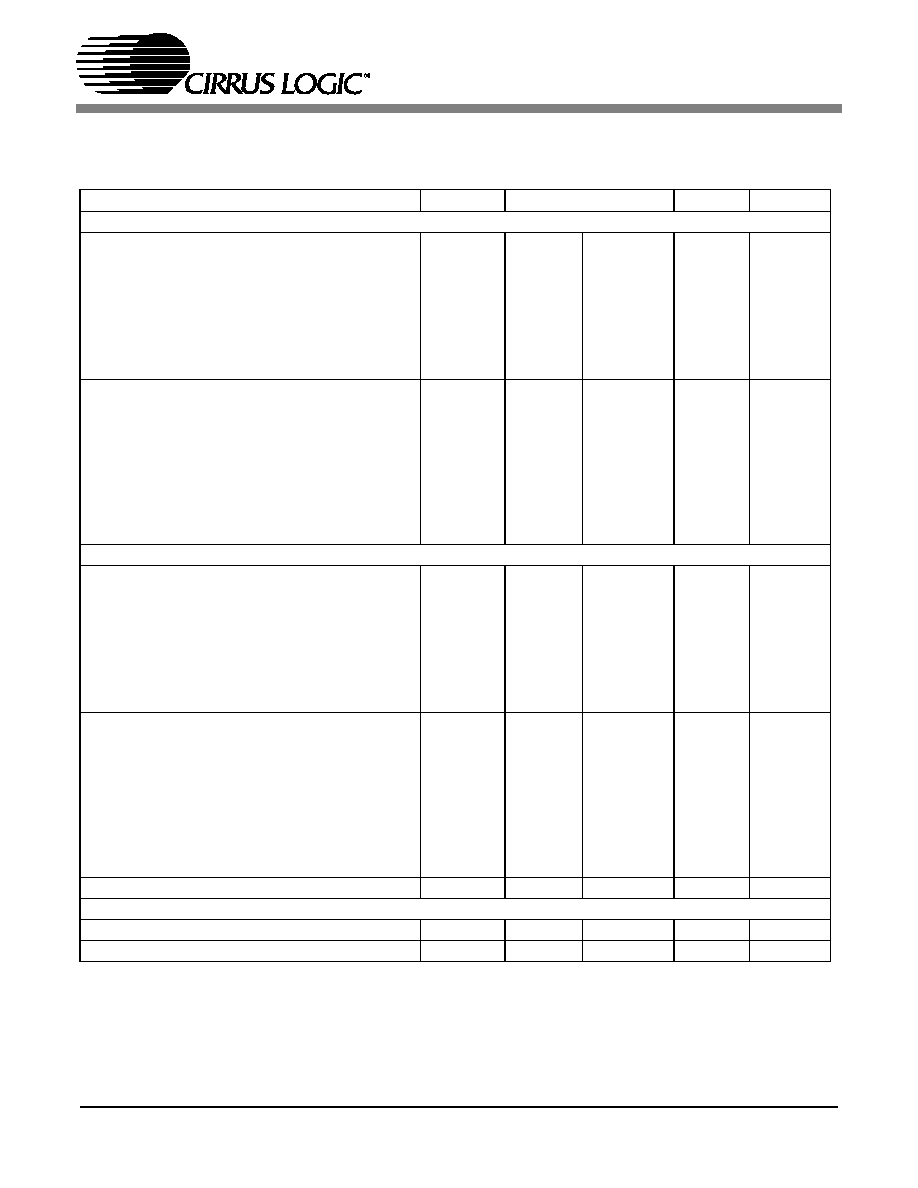
System Features
Direct interface with 1.8 V to 5 V logic levels
Optional asynchronous serial port operation
≠ Each serial port supports master or slave
operation
Selectable auxiliary analog output
≠ Allows analog monitoring of either the ADC
input signal after PGA or DAC output signal
Internal digital loopback
Power down mode
≠ Available for A/D, D/A, CODEC, Mic
Preamplifier
+3.3 V to +5 V analog power supply
+3.3 V to +5 V digital power supply
Supports I≤C and SPI control port interfaces
Pin-compatible with CS5345
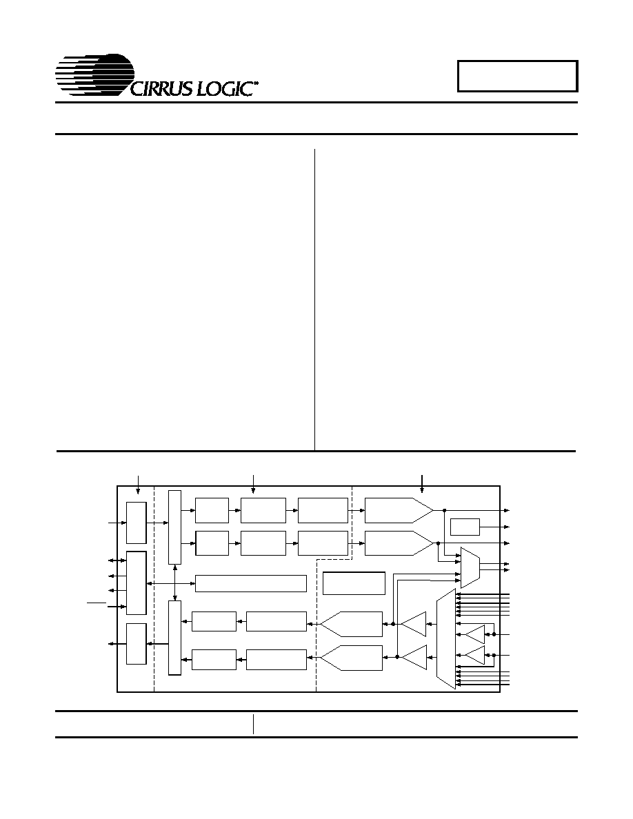
General Description
The CS4245 is a highly integrated stereo audio CO-
DEC. The CS4245 performs stereo analog-to-digital
(A/D) and digital-to-analog (D/A) conversion of up to
24-bit serial values at sample rates up to 192 kHz.
A 6:1 stereo input multiplexer is included for selecting
between line level or microphone level inputs. The mi-
crophone input path includes a +32 dB gain stage and a
low noise bias voltage supply. The PGA is available for
line or microphone inputs and provides gain/attenuation
of
±12 dB in 0.5 dB steps.
The output of the PGA is followed by an advanced 5th-
order, multi-bit delta sigma modulator and digital filter-
ing/decimation. Sampled data is transmitted by the
serial audio interface at rates from 4 kHz to 192 kHz in
either slave or master mode.
The D/A converter is based on a 4th-order multi-bit delta
sigma modulator with an ultra-linear low pass filter and
offers a volume control that operates with a 0.5 dB step
size. It incorporates selectable soft ramp and zero
crossing transition functions to eliminate clicks and
pops.
Standard 50/15
µs de-emphasis is available for a
44.1 kHz sample rate for compatibility with digital audio
programs mastered using the 50/15
µs pre-emphasis
technique.
Integrated level translators allow easy interfacing be-
tween the CS4245 and other devices operating over a
wide range of logic levels.
ORDERING INFORMATION
CS4245-CQZ -10∞ to 70∞ C
48-pin LQFP
CDB4245
Evaluation Board

CS4245
3
TABLE OF CONTENTS
1. PIN DESCRIPTIONS ............................................................................................................... 5
2. CHARACTERISTICS AND SPECIFICATIONS ....................................................................... 8
SPECIFIED OPERATING CONDITIONS ................................................................................. 8
ABSOLUTE MAXIMUM RATINGS ........................................................................................... 8
DAC ANALOG CHARACTERISTICS ....................................................................................... 9
DAC COMBINED INTERPOLATION & ON-CHIP ANALOG FILTER RESPONSE................ 10
ADC ANALOG CHARACTERISTICS ..................................................................................... 12
ADC ANALOG CHARACTERISTICS ..................................................................................... 14
ADC DIGITAL FILTER CHARACTERISTICS......................................................................... 15
AUXILIARY OUTPUT ANALOG CHARACTERISTICS .......................................................... 16
AUXILIARY OUTPUT ANALOG CHARACTERISTICS (CONT'D) ......................................... 17
AUXILIARY OUTPUT ANALOG CHARACTERISTICS (CONT'D) ......................................... 18
DC ELECTRICAL CHARACTERISTICS ................................................................................ 19
DIGITAL INTERFACE CHARACTERISTICS ......................................................................... 20
SWITCHING CHARACTERISTICS - SERIAL AUDIO PORT 1.............................................. 21
SWITCHING CHARACTERISTICS - SERIAL AUDIO PORT 2.............................................. 23
SWITCHING CHARACTERISTICS - CONTROL PORT - I≤C FORMAT ................................ 26
SWITCHING CHARACTERISTICS - CONTROL PORT - SPI FORMAT ............................... 27
3. TYPICAL CONNECTION DIAGRAM .................................................................................... 28
4. APPLICATIONS .................................................................................................................... 29
4.1 Recommended Power-Up Sequence ............................................................................. 29
4.2 System Clocking ............................................................................................................. 29
4.2.1 Synchronous / Asynchronous Mode .................................................................. 29
4.2.2 Master Clock ...................................................................................................... 29
4.2.3 Master Mode ...................................................................................................... 30
4.2.4 Slave Mode ........................................................................................................ 30
4.3 High Pass Filter and DC Offset Calibration .................................................................... 31
4.4 Analog Input Multiplexer, PGA, and Mic Gain ................................................................ 31
4.5 Input Connections ........................................................................................................... 32
4.6 Output Connections ........................................................................................................ 32
4.7 Output Transient Control ................................................................................................ 32
4.7.1 Power-up ............................................................................................................ 32
4.7.2 Power-down ....................................................................................................... 32
4.7.3 Serial Interface Clock Changes ......................................................................... 32
4.8 Auxiliary Analog Output .................................................................................................. 32
4.9 De-Emphasis Filter ......................................................................................................... 33
4.10 Internal Digital Loopback .............................................................................................. 33
4.11 Mute Control ................................................................................................................. 33
4.12 Control Port Description and Timing ............................................................................. 34
4.12.1 SPI Mode ......................................................................................................... 34
4.12.2 I≤C Mode .......................................................................................................... 35
4.13 Interrupts and Overflow ................................................................................................ 37
4.14 Reset ........................................................................................................................... 37
4.15 Synchronization of Multiple Devices ............................................................................. 37
4.16 Grounding and Power Supply Decoupling .................................................................... 37
5. REGISTER QUICK REFERENCE ......................................................................................... 38
6. REGISTER DESCRIPTION ................................................................................................... 39
6.1 Chip ID - Register 01h .................................................................................................... 39
6.2 Power Control - Address 02h ......................................................................................... 39
6.3 DAC Control - Address 03h ............................................................................................ 40
6.4 ADC Control - Address 04h ............................................................................................ 41
6.5 MCLK Frequency - Address 05h .................................................................................... 42

CS4245
4
6.6 Signal Selection - Address 06h ....................................................................................... 43
6.7 Channel A PGA Control - Address 07h ........................................................................... 43
6.8 Channel B PGA Control - Address 08h ........................................................................... 44
6.9 ADC Input Control - Address 09h ................................................................................... 44
6.10 DAC Channel A Volume Control - Address 0Ah ........................................................... 45
6.11 DAC Channel B Volume Control - Address 0Bh ........................................................... 45
6.12 DAC Control 2 - Address 0Ch ....................................................................................... 46
6.13 Interrupt Status - Address 0Dh ..................................................................................... 46
6.14 Interrupt Mask - Address 0Eh ....................................................................................... 47
6.15 Interrupt Mode MSB - Address 0Fh .............................................................................. 47
6.16 Interrupt Mode LSB - Address 10h ............................................................................... 47
7. PARAMETER DEFINITIONS ................................................................................................. 48
8. PACKAGE DIMENSIONS ...................................................................................................... 49
9. THERMAL CHARACTERISTICS AND SPECIFICATIONS ................................................. 49
Appendix A: DAC Filter Plots ......................................................................................... 50
Appendix B: ADC Filter Plots .............................................................................................. 52
CS4245
5
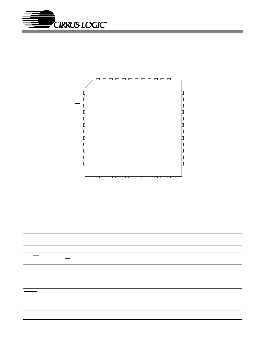
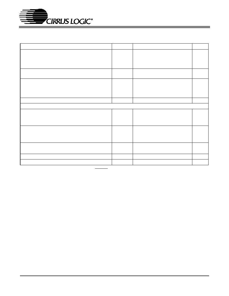
1. PIN DESCRIPTIONS
Pin Name
#
Pin Description
SDA/CDOUT
1
Serial Control Data (
Input/Output) - SDA is a data I/O in I≤C mode. CDOUT is the output data line for
the control port interface in SPI mode.
SCL/CCLK
2
Serial Control Port Clock (
Input) - Serial clock for the serial control port.
AD0/CS
3
Address Bit 0 (I≤C) / Control Port Chip Select (SPI)
(Input) - AD0 is a chip address pin in I≤C mode;
CS is the chip select signal for SPI format.
AD1/CDIN
4
Address Bit 1 (I≤C) / Serial Control Data Input (SPI)
(Input) - AD1 is a chip address pin in I≤C mode;
CDIN is the input data line for the control port interface in SPI mode.
VLC
5
Control Port Power (
Input) - Determines the required signal level for the control port interface. Refer
to the Recommended Operating Conditions for appropriate voltages.
RESET
6
Reset (
Input) - The device enters a low power mode when this pin is driven low.
AIN3A
AIN3B
7,
8
Stereo Analog Input 3 (
Input) - The full scale level is specified in the ADC Analog Characteristics
specification table.
1
2
3
4
5
6
7
8
9
10
11
12
13 14 15 16 17 18 19 20 21 22 23 24
48 47 46 45 44 43 42 41 40 39 38 37
36
35
34
33
32
31
30
29
28
27
26
25
VLS
SDA/CDOUT
AG
N
D
OV
F
L
SCL/CCLK
AD0/CS
AD1/CDIN
VLC
RESET
AIN3A
AIN3B
AIN2A
AIN2B
AIN1A
AIN1B
VA
AF
I
L
T
B
VQ
1
VQ
2
F
I
LT
1+
F
I
LT
2+
A
I
N4
A
/
M
I
CI
N1
A
I
N4
B
/
M
I
CI
N2
AIN
5
A
AIN
5
B
AF
I
L
T
A
MUTEC
AOUTB
AOUTA
AGND
AGND
VA
AUXOUTB
AUXOUTA
AIN6B
AIN6A
MICBIAS
IN
T
VD
DGND
MC
LK
1
L
RCK
1
SC
L
K
1
SD
O
U
T
MC
LK
2
L
RCK
2
SC
L
K
2
SD
I
N
CS4245
CS4245
6
AIN2A
AIN2B
9,
10
Stereo Analog Input 2 (
Input) - The full scale level is specified in the ADC Analog Characteristics
specification table.
AIN1A
AIN1B
11,
12
Stereo Analog Input 1 (
Input) - The full scale level is specified in the ADC Analog Characteristics
specification table.
AGND
13
Analog Ground (
Input) - Ground reference for the internal analog section.
VA
14
Analog Power
(Input) - Positive power for the internal analog section.
AFILTA
15
Antialias Filter Connection (
Output) - Antialias filter connection for the channel A ADC input.
AFILTB
16
Antialias Filter Connection (
Output) - Antialias filter connection for the channel B ADC input.
VQ1
17
Quiescent Voltage 1 (
Output) - Filter connection for the internal quiescent reference voltage.
VQ2
18
Quiescent Voltage 2 (
Output) - Filter connection for the internal quiescent reference voltage.
FILT1+
19
Positive Voltage Reference 1 (
Output) - Positive reference voltage for the internal sampling circuits.
FILT2+
20
Positive Voltage Reference 2 (
Output) - Positive reference voltage for the internal sampling circuits.
AIN4A/MICIN1
AIN4B/MICIN2
21,
22
Stereo Analog Input 4 / Microphone Input 1 & 2 (
Input) - The full scale level is specified in the ADC
Analog Characteristics specification table.
AIN5A
AIN5B
23,
24
Stereo Analog Input 5 (
Input) - The full scale level is specified in the ADC Analog Characteristics
specification table.
MICBIAS
25
Microphone Bias Supply (
Output) - Low noise bias supply for external microphone. Electrical charac-
teristics are specified in the DC Electrical Characteristics specification table.
AIN6A
AIN6B
26,
27
Stereo Analog Input 6 (
Input) - The full scale level is specified in the ADC Analog Characteristics
specification table.
AUXOUTA
AUXOUTB
28,
29
Auxiliary Analog Audio Output (
Output) - Analog output from either the DAC, the PGA block, or high
impedance. See "Auxiliary Output Source Select (Bits 6:5)" on page 43.
VA
30
Analog Power
(Input) - Positive power for the internal analog section.
AGND
31,
32
Analog Ground (
Input) - Ground reference for the internal analog section.
AOUTA
AOUTB
33,
34
DAC Analog Audio Output (
Output) - The full scale output level is specified in the DAC Analog Char-
acteristics specification table.
MUTEC
35
Mute Control
(Output) - This pin is active during power-up initialization, reset, muting, when master
clock to left/right clock frequency ratio is incorrect, or power-down.
VLS
36
Serial Audio Interface Power (
Input) - Determines the required signal level for the serial audio inter-
face. Refer to the Recommended Operating Conditions for appropriate voltages.
SDIN
37
Serial Audio Data Input (
Input) - Input for two's complement serial audio data.
SCLK2
38
Serial Port 2 Serial Bit Clock
(Input/Output) - Serial bit clock for serial audio interface 2.
LRCK2
39
Serial Port 2 Left Right Clock
(Input/Output) - Determines which channel, Left or Right, is currently
active on the serial audio input data line.
MCLK2
40
Master Clock 2 (
Input/Output) -Optional asynchronous clock source for the DAC's delta-sigma modu-
lators.
SDOUT
41
Serial Audio Data Output (
Output) - Output for two's complement serial audio data.
SCLK1
42
Serial Port 1 Serial Bit Clock
(Input/Output) - Serial bit clock for serial audio interface 1.
LRCK1
43
Serial Port 1 Left Right Clock
(Input/Output) - Determines which channel, Left or Right, is currently
active on the serial audio output data line.

CS4245
7
MCLK1
44
Master Clock 1 (
Input/Output) -Clock source for the ADC's delta-sigma modulators. By default, this
signal also clocks the DAC's delta-sigma modulators.
DGND
45
Digital Ground (
Input) - Ground reference for the internal digital section.
VD
46
Digital Power (
Input) - Positive power for the internal digital section.
INT
47
Interrupt (
Output) - Indicates an interrupt condition has occurred.
OVFL
48
ADC Overflow (
Output) - Indicates an ADC overflow condition is present.

CS4245
8
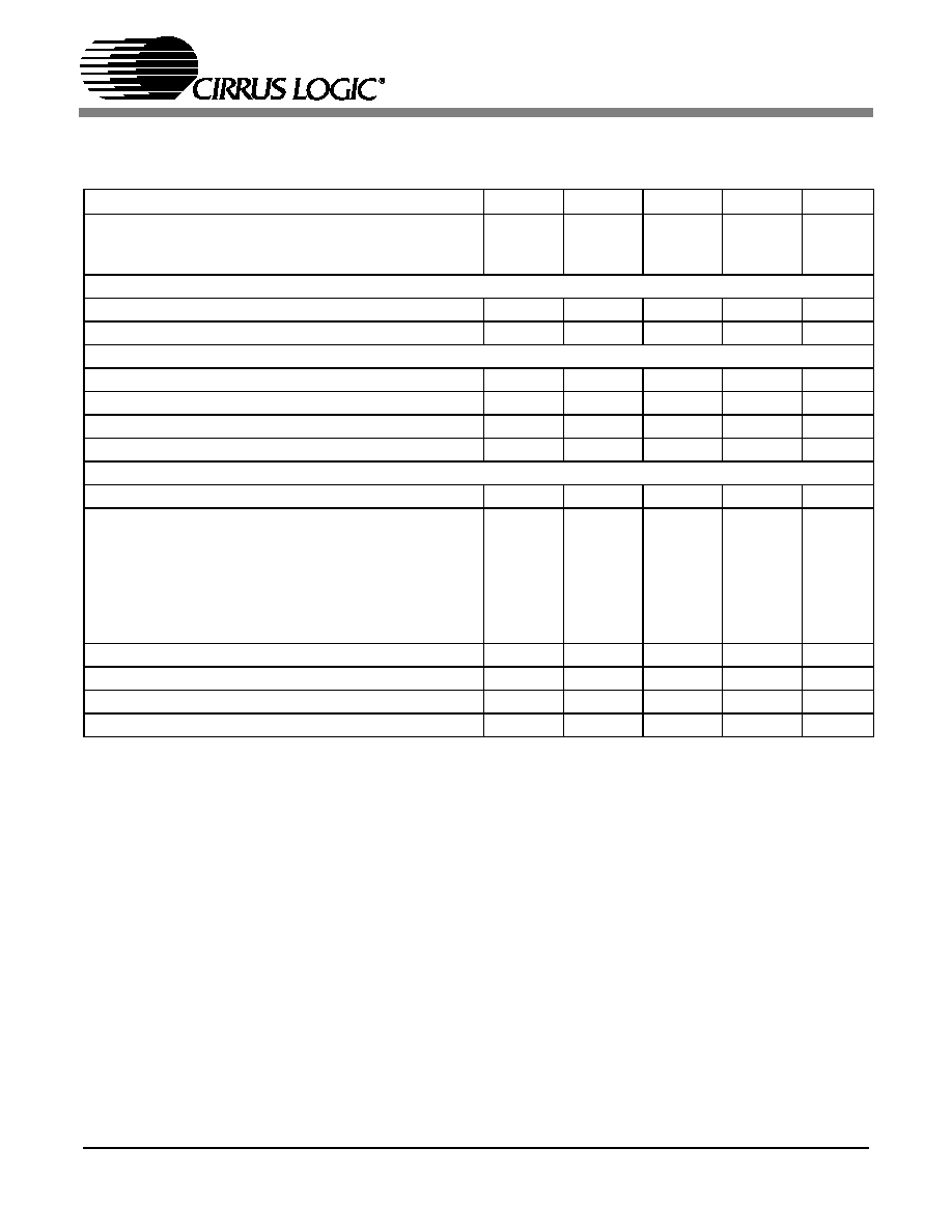
2. CHARACTERISTICS AND SPECIFICATIONS
(All Min/Max characteristics and specifications are guaranteed over the Specified Operating Conditions. Typical
performance characteristics and specifications are derived from measurements taken at nominal supply voltages
and T
A
= 25
∞C.)
SPECIFIED OPERATING CONDITIONS
(AGND = DGND = 0 V; All voltages with respect to
ground.)
ABSOLUTE MAXIMUM RATINGS
(AGND = DGND = 0 V All voltages with respect to ground.) (Note
1)
Notes: 1. Operation beyond these limits may result in permanent damage to the device.
Normal operation is not guaranteed at these extremes.
2. Any pin except supplies. Transient currents of up to ±100 mA on the analog input pins will not cause
SCR latch-up.
Parameters
Symbol Min Nom
Max
Units
DC Power Supplies:
Analog
Digital
Logic - Serial Port
Logic - Control Port
VA
VD
VLS
VLC
3.1
3.1
1.71
1.71
5.0
3.3
3.3
3.3
5.25
5.25
5.25
5.25
V
V
V
V
Ambient Operating Temperature (Power Applied)
T
A
-10
-
+70
∞C
Parameter
Symbol
Min
Typ
Max
Units
DC Power Supplies:
Analog
Digital
Logic - Serial Port
Logic - Control Port
VA
VD
VLS
VLC
-0.3
-0.3
-0.3
-0.3
-
-
-
-
+6.0
+6.0
+6.0
+6.0
V
V
V
V
Input Current
(Note 2)
I
in
-
-
±10
mA
Analog Input Voltage
V
INA
AGND-0.3
-
VA+0.3
V
Digital Input Voltage
Logic - Serial Port
Logic - Control Port
V
IND-S
V
IND-C
-0.3
-0.3
-
-
VLS+0.3
VLC+0.3
V
V
Ambient Operating Temperature (Power Applied)
T
A
-20
-
+85
∞C
Storage Temperature
T
stg
-65
-
+150
∞C
CS4245
9
DAC ANALOG CHARACTERISTICS
(Full-Scale Output Sine Wave, 997 Hz; Test load R
L
= 3 k
,
C
L
= 10 pF (see Figure 1), Fs = 48/96/192 kHz. Measurement Bandwidth 10 Hz to 20 kHz, unless otherwise speci-
fied.) Synchronous mode.
Note:
3. One-half LSB of triangular PDF dither added to data.
4. Guaranteed by design. The DC current draw represents the allowed current draw from the AOUT pin
due to typical leakage through the electrolytic DC blocking capacitors.
5. Guaranteed by design. See Figure 2. R
L
and C
L
reflect the recommended minimum resistance and
maximum capacitance required for the internal op-amp's stability. C
L
affects the dominant pole of the
internal output amp; increasing C
L
beyond 100 pF can cause the internal op-amp to become unstable.
Parameter
All Speed Modes
Symbol
Min
Typ
Max
Unit
Dynamic Performance for VA = 5 V
Dynamic Range
(Note 3)
18 to 24-Bit
unweighted
A-Weighted
16-Bit
unweighted
A-Weighted
96
99
87
90
102
105
93
96
-
-
-
-
dB
dB
dB
dB
Total Harmonic Distortion + Noise
(Note 3)
18 to 24-Bit
0 dB
-20 dB
-60 dB
16-Bit
0 dB
-20 dB
-60 dB
THD+N
-
-
-
-
-
-
-95
-82
-42
-93
-73
-33
-89
-76
-36
-87
-67
-27
dB
dB
dB
dB
dB
dB
Dynamic Performance for VA = 3.3 V
Dynamic Range
(Note 3)
18 to 24-Bit
unweighted
A-Weighted
16-Bit
unweighted
A-Weighted
93
96
85
88
99
102
90
93
-
-
-
-
dB
dB
dB
dB
Total Harmonic Distortion + Noise
(Note 3)
18 to 24-Bit
0 dB
-20 dB
-60 dB
16-Bit
0 dB
-20 dB
-60 dB
THD+N
-
-
-
-
-
-
-92
-79
-39
-90
-70
-30
-84
-71
-31
-82
-62
-22
dB
dB
dB
dB
dB
dB
Interchannel Isolation
(1 kHz)
-
100
-
dB
DC Accuracy
Interchannel Gain Mismatch
-
0.1
0.25
dB
Gain Drift
-
100
-
ppm/∞C
Analog Output
Full Scale Output Voltage
0.60*VA
0.65*VA
0.70*VA
V
pp
DC Current draw from an AOUT pin
(Note 4)
I
OUT
-
-
10
µA
AC-Load Resistance
(Note 5)
R
L
3
-
-
k
Load Capacitance
(Note 5)
C
L
-
-
100
pF
Output Impedance
Z
OUT
-
100
-
CS4245
10
DAC COMBINED INTERPOLATION & ON-CHIP ANALOG FILTER RESPONSE
Notes: 6. Filter response is guaranteed by design.
7. For Single Speed Mode, the Measurement Bandwidth is 0.5465 Fs to 3 Fs.
For Double Speed Mode, the Measurement Bandwidth is 0.577 Fs to 1.4 Fs.
For Quad Speed Mode, the Measurement Bandwidth is 0.7 Fs to 1 Fs.
8. De-emphasis is available only in Single Speed Mode.
9. Response is clock dependent and will scale with Fs. Note that the amplitude vs. frequency plots of this
data (Figures 21 to 30) have been normalized to Fs and can be de-normalized by multiplying the X-axis
scale by Fs.
Parameter (Note 6,9)
Symbol
Min
Typ
Max
Unit
Combined Digital and On-chip Analog Filter Response Single Speed Mode
Passband (Note 6)
to -0.05 dB corner
to -3 dB corner
0
0
-
-
.4780
.4996
Fs
Fs
Frequency Response 10 Hz to 20 kHz
-.01
-
+.08
dB
StopBand
.5465
-
-
Fs
StopBand Attenuation
(Note 7)
50
-
-
dB
Group Delay
tgd
-
10/Fs
-
s
De-emphasis Error (Note 8)
Fs = 44.1 kHz
-
-
+.05/-.25
dB
Combined Digital and On-chip Analog Filter Response Double Speed Mode
Passband (Note 6)
to -0.1 dB corner
to -3 dB corner
0
0
-
-
.4650
.4982
Fs
Fs
Frequency Response 10 Hz to 20 kHz
-.05
-
+.2
dB
StopBand
.5770
-
-
Fs
StopBand Attenuation
(Note 7)
55
-
-
dB
Group Delay
tgd
-
5/Fs
-
s
Combined Digital and On-chip Analog Filter Response Quad Speed Mode
Passband (Note 6)
to -0.1 dB corner
to -3 dB corner
0
0
-
-
0.397
0.476
Fs
Fs
Frequency Response 10 Hz to 20 kHz
0
-
+0.00004
dB
StopBand
0.7
-
-
Fs
StopBand Attenuation
(Note 7)
51
-
-
dB
Group Delay
tgd
-
2.5/Fs
-
s
CS4245
11
AOUTx
AGND
3.3 µF
V
out
R
L
C
L
Figure 1. DAC Output Test Load
100
50
75
25
2.5
5
10
15
Safe Operating
Region
C
a
p
a
ci
t
i
ve
Loa
d -
-
C
(
p
F
)
L
Resistive Load -- R (k
)
L
125
3
20
Figure 2. Maximum DAC Loading
CS4245
12
ADC ANALOG CHARACTERISTICS
Test conditions (unless otherwise specified): Input test sig-
nal is a 1 kHz sine wave; measurement bandwidth is 10 Hz to 20 kHz. Fs = 48/96/192 kHz. Synchronous mode.
Line Level Inputs
Parameter
Symbol
Min
Typ Max
Unit
Dynamic Performance for VA = 5 V
Dynamic Range
PGA Setting: -12 dB to +6 dB
A-weighted
unweighted
(Note 12) 40 kHz bandwidth unweighted
PGA Setting: +12 dB Gain
A-weighted
unweighted
(Note 12) 40 kHz bandwidth unweighted
99
96
-
93
90
-
105
102
99
99
96
93
-
-
-
-
-
-
dB
dB
dB
dB
dB
dB
Total Harmonic Distortion + Noise (Note 11)
PGA Setting: -12 dB to +6 dB
-1 dB
-20 dB
-60 dB
(Note 12) 40 kHz bandwidth -1 dB
PGA Setting: +12 dB Gain
-1 dB
-20 dB
-60 dB
(Note 12) 40 kHz bandwidth -1 dB
THD+N
-
-
-
-
-
-
-
-
-95
-82
-42
-92
-92
-76
-36
-89
-89
-
-
-
-86
-
-
-
dB
dB
dB
dB
dB
dB
dB
dB
Dynamic Performance for VA = 3.3 V
Dynamic Range
PGA Setting: -12 dB to +6 dB
A-weighted
unweighted
(Note 12) 40 kHz bandwidth unweighted
PGA Setting: +12 dB Gain
A-weighted
unweighted
(Note 12) 40 kHz bandwidth unweighted
94
91
-
90
87
-
102
99
96
96
93
90
-
-
-
-
-
-
dB
dB
dB
dB
dB
dB
CS4245
13
10. Valid for the selected input pair.
Total Harmonic Distortion + Noise (Note 11)
PGA Setting: -12 dB to +6 dB
-1 dB
-20 dB
-60 dB
(Note 12) 40 kHz bandwidth -1 dB
PGA Setting: +12 dB Gain
-1 dB
-20 dB
-60 dB
(Note 12) 40 kHz bandwidth -1 dB
THD+N
-
-
-
-
-
-
-
-
-92
-79
-39
-84
-89
-73
-33
-81
-86
-
-
-
-83
-
-
-
dB
dB
dB
dB
dB
dB
dB
dB
Line Level Inputs
Parameter
Symbol
Min
Typ Max
Unit
Interchannel Isolation
-
90
-
dB
Line Level Input Characteristics
Full-scale Input Voltage
0.53*VA
0.56*VA
0.59*VA
V
pp
Input Impedance
(Note 10)
6.12
6.8
7.48
k
Maximum Interchannel Input Impedance Mis-
match
-
5
-
%
Line Level and Microphone Level Inputs
Parameter
Symbol
Min
Typ Max
Unit
DC Accuracy
Interchannel Gain Mismatch
-
0.1
-
dB
Gain Error
-
±
5
%
Gain Drift
-
±
100
-
ppm/∞C
Programmable Gain Characteristics
Gain Step Size
-
0.5
-
dB
Absolute Gain Step Error
-
-
0.4
dB
CS4245
14
ADC ANALOG CHARACTERISTICS
(cont)
11. Referred to the typical line level full-scale input voltage
12. Valid for Double and Quad Speed Modes only.
13. Valid when the microphone level inputs are selected.
Microphone Level Inputs
Parameter
Symbol
Min
Typ Max
Unit
Dynamic Performance for VA = 5 V
Dynamic Range
PGA Setting: -12 dB to 0 dB
A-weighted
unweighted
PGA Setting: +12 dB
A-weighted
unweighted
77
74
65
62
83
80
71
68
-
-
-
-
dB
dB
dB
dB
Total Harmonic Distortion + Noise (Note 11)
PGA Setting: -12 dB to 0 dB
-1 dB
-20 dB
-60 dB
PGA Setting: +12 dB
-1 dB
THD+N
-
-
-
-
-80
-60
-20
-68
-74
-
-
-
dB
dB
dB
dB
Dynamic Performance for VA = 3.3 V
Dynamic Range
PGA Setting: -12 dB to 0 dB
A-weighted
unweighted
PGA Setting: +12 dB
A-weighted
unweighted
77
74
65
62
83
80
71
68
-
-
-
-
dB
dB
dB
dB
Total Harmonic Distortion + Noise (Note 11)
PGA Setting: -12 dB to 0 dB
-1 dB
-20 dB
-60 dB
PGA Setting: +12 dB
-1 dB
THD+N
-
-
-
-
-80
-60
-20
-68
-74
-
-
-
dB
dB
dB
dB
Interchannel Isolation
-
30
-
dB
Microphone Level Input Characteristics
Full-scale Input Voltage
0.013*VA
0.014*VA
0.015*VA
V
pp
Input Impedance
(Note 13)
-
100
-
k
CS4245
15
ADC DIGITAL FILTER CHARACTERISTICS
Note: 14. Filter response is guaranteed by design.
15. Response shown is for Fs equal to 48 kHz.
16. Response is clock dependent and will scale with Fs. Note that the response plots (Figures 33 to 44) are
normalized to Fs and can be de-normalized by multiplying the X-axis scale by Fs.
Parameter (Note 14, 16)
Symbol
Min
Typ
Max
Unit
Single Speed Mode
Passband
(-0.1 dB)
0
-
0.4896
Fs
Passband Ripple
-
-
0.035
dB
Stopband
0.5688
-
-
Fs
Stopband Attenuation
70
-
-
dB
Total Group Delay (Fs = Output Sample Rate)
t
gd
-
12/Fs
-
s
Double Speed Mode
Passband
(-0.1 dB)
0
-
0.4896
Fs
Passband Ripple
-
-
0.025
dB
Stopband
0.5604
-
-
Fs
Stopband Attenuation
69
-
-
dB
Total Group Delay (Fs = Output Sample Rate)
t
gd
-
9/Fs
-
s
Quad Speed Mode
Passband
(-0.1 dB)
0
-
0.2604
Fs
Passband Ripple
-
-
0.025
dB
Stopband
0.5000
-
-
Fs
Stopband Attenuation
60
-
-
dB
Total Group Delay (Fs = Output Sample Rate)
t
gd
-
5/Fs
-
s
High Pass Filter Characteristics
Frequency Response
-3.0 dB
-0.13 dB
(Note 15)
-
1
20
-
-
Hz
Hz
Phase Deviation
@ 20Hz
(Note 15)
-
10
-
Deg
Passband Ripple
-
-
0
dB
Filter Settling Time
10
5
/Fs
s
CS4245
16
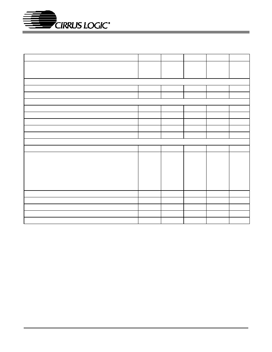
AUXILIARY OUTPUT ANALOG CHARACTERISTICS
Test conditions (unless otherwise
specified): Synchronous mode, Fs = 48/96/192 kHz. Input test signal is a 1 kHz sine wave; measurement bandwidth
is 10 Hz to 20 kHz.
VA = 5 V
Parameter
Symbol
Min
Typ Max
Unit
Dynamic Performance with PGA Output Selected, Line Level Input
Dynamic Range
(Note 18)
PGA Setting: -12 dB to +6 dB
A-weighted
unweighted
PGA Setting: +12 dB Gain
A-weighted
unweighted
99
96
93
90
105
102
99
96
-
-
-
-
dB
dB
dB
dB
Total Harmonic Distortion + Noise
(Note 18)
PGA Setting: -12 dB to +12 dB
-1 dB
-20 dB
-60 dB
THD+N
-
-
-
-80
-82
-42
-74
-
-
dB
dB
dB
Dynamic Performance with PGA Output Selected, Mic Level Input
Dynamic Range
(Note 18)
PGA Setting: -12 dB to 0 dB
A-weighted
unweighted
PGA Setting: +12 dB
A-weighted
unweighted
77
74
65
62
83
80
71
68
-
-
-
-
dB
dB
dB
dB
Total Harmonic Distortion + Noise
(Note 18)
PGA Setting: -12 dB to 0 dB
-1 dB
-20 dB
-60 dB
PGA Setting: +12 dB
-1 dB
THD+N
-
-
-
-
-74
-60
-20
-68
-68
-
-
-
dB
dB
dB
dB
Dynamic Performance with DAC Output Selected
Dynamic Range
(Notes 17, 18)
18 to 24-Bit
A-Weighted
unweighted
16-Bit
A-Weighted
unweighted
99
96
90
87
105
102
96
93
-
-
-
-
dB
dB
dB
dB
Total Harmonic Distortion + Noise
(Notes 17, 18)
16 to 24-Bit
0 dB
-20 dB
-60 dB
THD+N
-
-
-
-80
-82
-42
-74
-
-
dB
dB
dB

CS4245
17
AUXILIARY OUTPUT ANALOG CHARACTERISTICS (CONT'D)
Notes: 17. One-half LSB of triangular PDF dither added to data.
18. Referred to the typical AUXOUT Full-Scale Output Voltage.
VA = 3.3 V
Parameter
Symbol
Min
Typ Max
Unit
Dynamic Performance with PGA Output Selected, Line Level Input
Dynamic Range
(Note 18)
PGA Setting: -12 dB to +6 dB
A-weighted
unweighted
PGA Setting: +12 dB Gain
A-weighted
unweighted
94
91
90
87
102
99
96
93
-
-
-
-
dB
dB
dB
dB
Total Harmonic Distortion + Noise
(Note 18)
PGA Setting: -12 dB to +12 dB
-1 dB
-20 dB
-60 dB
THD+N
-
-
-
-80
-82
-42
-74
-
-
dB
dB
dB
Dynamic Performance with PGA Output Selected, Mic Level Input
Dynamic Range
(Note 18)
PGA Setting: -12 dB to 0 dB
A-weighted
unweighted
PGA Setting: +12 dB
A-weighted
unweighted
77
74
65
62
83
80
71
68
-
-
-
-
dB
dB
dB
dB
Total Harmonic Distortion + Noise
(Note 18)
PGA Setting: -12 dB to 0 dB
-1 dB
-20 dB
-60 dB
PGA Setting: +12 dB
-1 dB
THD+N
-
-
-
-
-74
-60
-20
-68
-68
-
-
-
dB
dB
dB
dB
Dynamic Performance with DAC Output Selected
Dynamic Range
(Notes 17, 18)
18 to 24-Bit
A-Weighted
unweighted
16-Bit
A-Weighted
unweighted
96
93
88
85
102
99
93
90
-
-
-
-
dB
dB
dB
dB
Total Harmonic Distortion + Noise
(Notes 17, 18)
16 to 24-Bit
0 dB
-20 dB
-60 dB
THD+N
-
-
-
-80
-82
-42
-74
-
-
dB
dB
dB
CS4245
18
AUXILIARY OUTPUT ANALOG CHARACTERISTICS (CONT'D)
Notes: 19. Valid only when PGA output is selected.
VA = 5 V or 3.3 V
Parameter
Symbol
Min
Typ Max
Unit
DC Accuracy
Interchannel Gain Mismatch
-
0.1
-
dB
Gain Error
-
±
5
-
%
Gain Drift
-
±
100
-
ppm/∞C
Analog Output
Full-Scale Output Voltage
PGA Output Selected
DAC Output Selected
-
-
0.56*VA
0.7*VA
VA
0.75*VA
V
pp
V
pp
Frequency Response 10 Hz to 20 kHz
-0.1dB
-
+0.1dB
dB
Analog In to Analog Out Phase Shift
(Note 19)
-
180
-
deg
DC Current draw from an AUXOUT pin
I
OUT
-
-
1
µA
AC-Load Resistance
R
L
100
-
-
k
Load Capacitance
C
L
-
-
20
pF
Output Impedance
Z
OUT
-
1
-
k
CS4245
19
DC ELECTRICAL CHARACTERISTICS
(AGND = DGND = 0 V, all voltages with respect to
ground. MCLK=12.288 MHz; Fs=48 kHz, Master Mode)
Notes: 20. Power Down Mode is defines as RESET = Low with all clock and data lines held static and no analog
input.
21. Valid with the recommended capacitor values on FILT1+, FILT2+, VQ1 and VQ2 as shown in the
Typical Connection Diagram.
22. Guaranteed by design. The DC current draw represents the allowed current draw due to typical leakage
through the electrolytic de-coupling capacitors.
Parameter
Symbol
Min
Typ
Max
Unit
Power Supply Current VA = 5 V
(Normal Operation) VA = 3.3 V
VD, VLS, VLC = 5 V
VD, VLS, VLC = 3.3 V
I
A
I
A
I
D
I
D
-
-
-
-
41
37
39
23
50
45
47
28
mA
mA
mA
mA
Power Supply Current.
VA = 5 V
(Power-Down Mode) (Note 20).
VLS, VLC, VD=5 V
I
A
I
D
-
-
0.50
0.54
-
-
mA
mA
Power Consumption
(Normal Operation).
VA, VD, VLS, VLC = 5 V
VA, VD, VLS, VLC = 3.3 V
(Power-Down Mode).
VA, VD, VLS, VLC = 5 V
-
-
-
-
-
-
400
198
4.2
485
241
-
mW
mW
mW
Power Supply Rejection Ratio
(1 kHz)
(Note 21)
PSRR
-
60
-
dB
VQ Characteristics
Quiescent Voltage 1
VQ1
-
0.5 x VA
-
VDC
DC Current from VQ1
(Note 22)
I
Q1
-
-
1
µA
VQ1 Output Impedance
Z
Q1
-
23
-
k
Quiescent Voltage 2
VQ2
-
0.5 x VA
-
VDC
DC Current from VQ2
(Note 22)
I
Q2
-
-
1
µA
VQ2 Output Impedance
Z
Q2
-
23
-
k
FILT1+ Nominal Voltage
FILT1+
-
VA
-
VDC
FILT2+ Nominal Voltage
FILT2+
-
VA
-
VDC
Microphone Bias Voltage
MICBIAS
-
0.8 x VA
-
VDC
Current from MICBIAS
I
MB
-
-
2
mA

CS4245
20
DIGITAL INTERFACE CHARACTERISTICS
Notes: 23. Serial Port signals include: MCLK1, MCLK2, SCLK1, SCLK2, LRCK1, LRCK2, SDIN, SDOUT.
Control Port signals include: SCL/CCLK, SDA/CDOUT, AD0/CS, AD1/CDIN, RESET, INT, OVFL.
24. Guaranteed by design.
Parameters (Note 23)
Symbol
Min
Typ
Max
Units
High-Level Input Voltage
Serial Port
Control Port
V
IH
V
IH
0.7xVLS
0.7xVLC
-
-
-
-
V
V
Low-Level Input Voltage
Serial Port
Control Port
V
IL
V
IL
-
-
-
-
0.2xVLS
0.2xVLC
V
V
High-Level Output Voltage at I
o
=2 mA
Serial Port
Control Port
MUTEC
V
OH
V
OH
V
OH
VLS-1.0
VLC-1.0
VA-1.0
-
-
-
-
-
-
V
V
V
Low-Level Output Voltage at I
o
=2 mA
Serial Port
Control Port
MUTEC
V
OL
V
OL
V
OL
-
-
-
-
-
-
0.4
0.4
0.4
V
V
V
Input Leakage Current
I
in
-
-
±10
µA
Input Capacitance
(Note 24)
-
-
1
pF
Maximum MUTEC Drive Current
-
3
-
mA
Minimum OVFL Active Time
µs
10
6
LRCK1
--------------------
CS4245
21
SWITCHING CHARACTERISTICS - SERIAL AUDIO PORT 1
(Logic `0' = DGND = 0 V;
Logic `1' = VL, C
L
= 20 pF)
(Note 25)
25. See figures 3 and 4 on page 22.
Parameter
Symbol
Min
Typ
Max
Unit
Sample Rate
Single Speed Mode
Double Speed Mode
Quad Speed Mode
Fs
Fs
Fs
4
50
100
-
-
-
50
100
200
kHz
kHz
kHz
MCLK Specifications
MCLK1 Input Frequency
f
mclk
1.024
-
51.200
MHz
MCLK1 Input Pulse Width High/Low
t
clkhl
8
-
-
ns
Master Mode
LRCK1 Duty Cycle
-
50
-
%
SCLK1 Duty Cycle
-
50
-
%
SCLK1 falling to LRCK1 edge
t
slr
-10
-
10
ns
SCLK1 falling to SDOUT valid
t
sdo
0
-
32
ns
Slave Mode
LRCK1 Duty Cycle
40
50
60
%
SCLK1 Period
Single Speed Mode
Double Speed Mode
Quad Speed Mode
t
sclkw
t
sclkw
t
sclkw
-
-
-
-
-
-
ns
ns
ns
SCLK1 Pulse Width High
t
sclkh
30
-
-
ns
SCLK1 Pulse Width Low
t
sclkl
48
-
-
ns
SCLK1 falling to LRCK1 edge
t
slr
-10
-
10
ns
SCLK1 falling to SDOUT valid
t
sdo
0
-
32
ns
10
9
128
(
)Fs
---------------------
10
9
64
( )Fs
------------------
10
9
64
( )Fs
------------------
CS4245
22
slr
t
SDOUT
SCLK1
Output
LRCK1
Output
sdo
t
slr
t
SDOUT
SCLK1
Input
LRCK1
Input
sdo
t
sclkh
t
sclkl
t
sclkw
t
Figure 3. Master Mode Timing - Serial Audio Port 1
Figure 4. Slave Mode Timing - Serial Audio Port 1
CS4245
23
SWITCHING CHARACTERISTICS - SERIAL AUDIO PORT 2
(Logic `0' = DGND = 0 V;
Logic `1' = VL, C
L
= 20 pF) (Note 26)
26. See figures 5 and 6 on page 24.
Parameter
Symbol
Min
Typ
Max
Unit
Sample Rate
Single Speed Mode
Double Speed Mode
Quad Speed Mode
Fs
Fs
Fs
4
50
100
-
-
-
50
100
200
kHz
kHz
kHz
MCLK Specifications
MCLK2 Input Frequency
f
mclk
1.024
-
51.200
MHz
MCLK2 Input Pulse Width High/Low
t
clkhl
8
-
-
ns
Master Mode
LRCK2 Duty Cycle
-
50
-
%
SCLK2 Duty Cycle
-
50
-
%
SCLK2 falling to LRCK edge
t
slr
-10
-
10
ns
SDIN valid to SCLK2 rising setup time
t
sdis
16
-
-
ns
SCLK2 rising to SDIN hold time
t
sdih
20
-
-
ns
Slave Mode
LRCK2 Duty Cycle
40
50
60
%
SCLK2 Period
Single Speed Mode
Double Speed Mode
Quad Speed Mode
t
sclkw
t
sclkw
t
sclkw
-
-
-
-
-
-
ns
ns
ns
SCLK2 Pulse Width High
t
sclkh
30
-
-
ns
SCLK2 Pulse Width Low
t
sclkl
48
-
-
ns
SCLK2 falling to LRCK2 edge
t
slr
-10
-
10
ns
SDIN valid to SCLK2 rising setup time
t
sdis
16
-
-
ns
SCLK2 rising to SDIN hold time
t
sdih
20
-
-
ns
10
9
128
(
)Fs
---------------------
10
9
64
( )Fs
------------------
10
9
64
( )Fs
------------------
CS4245
24
sdis
t
slr
t
SCLK2
Output
LRCK2
Output
SDIN
sdih
t
sdis
t
slr
t
SCLK2
Input
LRCK2
Input
SDIN
sdih
t
sclkh
t
sclkl
t
sclkw
t
Figure 5. Master Mode Timing - Serial Audio Port 2
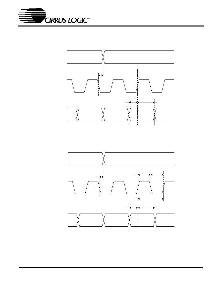
Figure 6. Slave Mode Timing - Serial Audio Port 2
CS4245
25
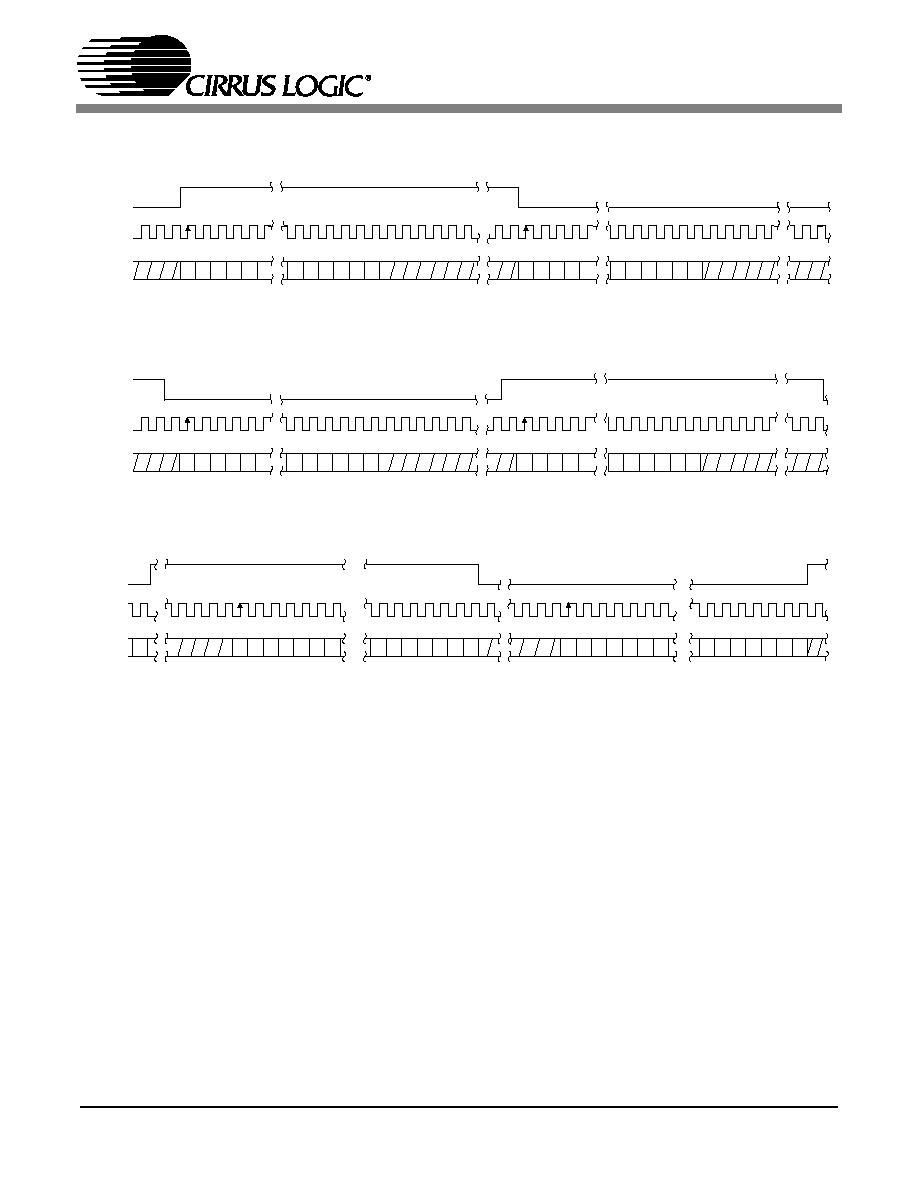
Figure 7. Format 0, Left Justified up to 24-Bit Data
LRCK
SCLK
Left Channel
Right Channel
SDATA
+3 +2 +1 LSB
+5 +4
MSB -1 -2 -3 -4 -5
+3 +2 +1 LSB
+5 +4
MSB -1 -2 -3 -4
Channel A - Left
Channel B - Right
Figure 8. Format 1, I≤S up to 24-Bit Data
LRCK
SCLK
Left Channel
Right Channel
SDATA
+3 +2 +1 LSB
+5 +4
MSB -1 -2 -3 -4 -5
+3 +2 +1 LSB
+5 +4
MSB -1 -2 -3 -4
Channel A - Left
Channel B - Right
LRCK
SCLK
Left Channel
SDATA
+5 +4 +3 +2 +1 LSB
MSB-1 -2 -3 -4 -5
32 clocks
Right Channel
LSB
+5 +4 +3 +2 +1 LSB
MSB -1 -2 -3 -4 -5
+6
-6
+6
-6
Channel A - Left
Channel B - Right
Figure 9. Format 2, Right Justified 16-Bit Data.
Format 3, Right Justified 24-Bit Data.
CS4245
26
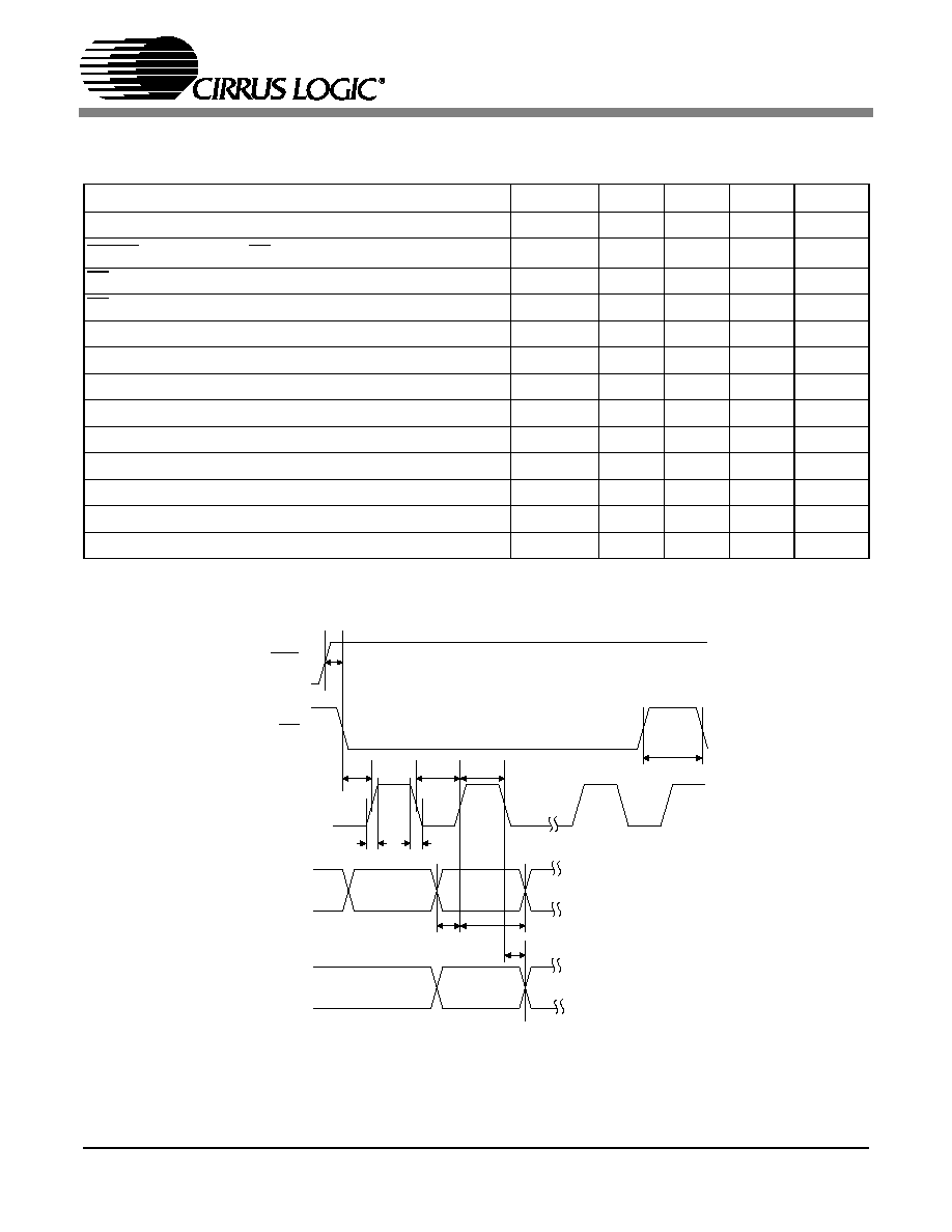
SWITCHING CHARACTERISTICS - CONTROL PORT - I≤C FORMAT
(Inputs: Logic 0 = DGND, Logic 1 = VLC, C
L
= 30 pF)
Notes: 27. Data must be held for sufficient time to bridge the transition time, t
fc
, of SCL.
28. Guaranteed by design.
Parameter Symbol
Min
Max
Unit
SCL Clock Frequency
f
scl
-
100
kHz
RESET Rising Edge to Start
t
irs
500
-
ns
Bus Free Time Between Transmissions
t
buf
4.7
-
µs
Start Condition Hold Time (prior to first clock pulse)
t
hdst
4.0
-
µs
Clock Low time
t
low
4.7
-
µs
Clock High Time
t
high
4.0
-
µs
Setup Time for Repeated Start Condition
t
sust
4.7
-
µs
SDA Hold Time from SCL Falling
(Note 27)
t
hdd
0
-
µs
SDA Setup time to SCL Rising
t
sud
250
-
ns
Rise Time of SCL and SDA
(Note 28)
t
rc
-
1
µs
Fall Time SCL and SDA
(Note 28)
t
fc
-
300
ns
Setup Time for Stop Condition
t
susp
4.7
-
µs
Acknowledge Delay from SCL Falling
t
ack
300
1000
ns
t
buf
t
hdst
t
l o w
t
hdd
t
high
t
sud
Stop
S tart
S D A
S C L
t
irs
R S T
t
hdst
t
rc
t fc
t sust
t susp
Sta rt
Stop
R ep e a te d
t
rd
t
fd
t
ack
Figure 10. Control Port Timing - I≤C Format
CS4245
27
SWITCHING CHARACTERISTICS - CONTROL PORT - SPI FORMAT
(Inputs: Logic 0 = DGND, Logic 1 = VLC, C
L
= 30 pF)
Notes: 29. Data must be held for sufficient time to bridge the transition time of CCLK.
30. For f
sck
<1 MHz.
Parameter
Symbol Min Typ
Max
Units
CCLK Clock Frequency
f
sck
0
-
6.0
MHz
RESET Rising Edge to CS Falling.
t
srs
500
-
ns
CS High Time Between Transmissions
t
csh
1.0
-
-
µs
CS Falling to CCLK Edge
t
css
20
-
-
ns
CCLK Low Time
t
scl
66
-
-
ns
CCLK High Time
t
sch
66
-
-
ns
CDIN to CCLK Rising Setup Time
t
dsu
40
-
-
ns
CCLK Rising to DATA Hold Time
(Note 29)
t
dh
15
-
-
ns
CCLK Falling to CDOUT Stable
t
pd
-
-
50
ns
Rise Time of CDOUT
t
r1
-
-
25
ns
Fall Time of CDOUT
t
f1
-
-
25
ns
Rise Time of CCLK and CDIN
(Note 30)
t
r2
-
-
100
ns
Fall Time of CCLK and CDIN
(Note 30)
t
f2
-
-
100
ns
t r2
t f2
t dsu
t dh
t sch
t scl
CS
CCLK
CDIN
t css
t pd
CDOUT
t csh
RST
t srs
Figure 11. Control Port Timing - SPI Format
CS4245
28
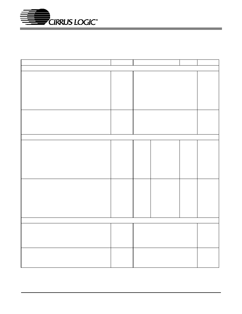
3.
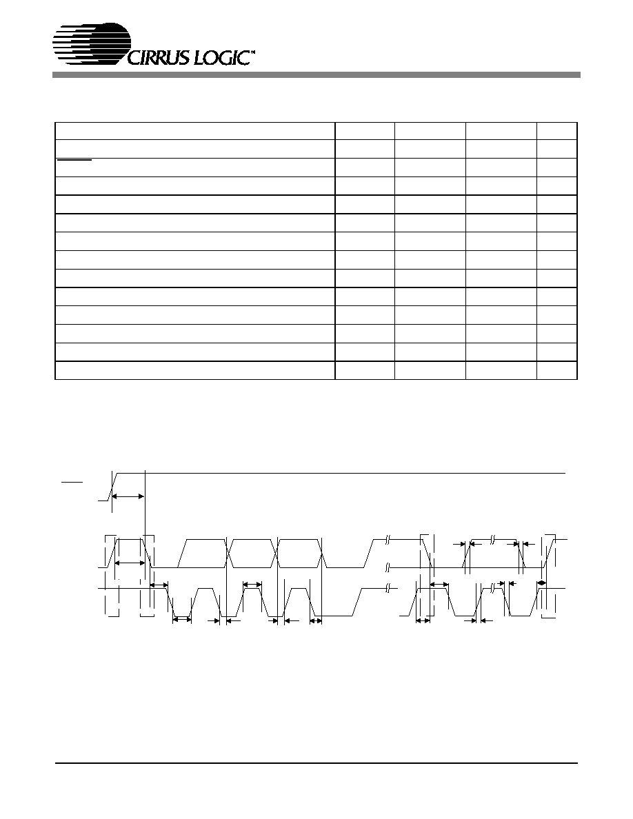
TYPICAL CONNECTION DIAGRAM
VLS
0.1 µF
+1.8V
to +5V
MUTEC
Mute
Drive
DGND
VLC
0.1 µF
+1.8V
to +5V
SCL/CCLK
SDA/CDOUT
AD1/CDIN
RESET
2 k
See Note 1
LRCK2
SDIN
AGND
AD0/CS
Note 1: Resistors are required for I≤C control
port operation
Digital Audio
Playback
Micro-
Controller
MCLK2
SCLK2
* Capacitors must be C0G or equivalent
Digital Audio
Capture
LRCK1
SDOUT
MCLK1
SCLK1
AUXOUTA
AUXOUTB
2.2nF
AFILTA
AFILTB
OVFL
2.2nF
3.3 µF
3.3 µF
47 µF
0.1 µF
VQ1
FILT1+
10 µF
AGND
*
*
AOUTA
AOUTB
470
470
3.3 µF
C
Optional
Analog
Muting
2 k
3.3 µF
INT
47 µF
10 k
10 k
C
R
ext
R
ext
See Note 2
For best response to Fs/2 :
(
)
470
4
470
◊
+
=
ext
ext
R
Fs
R
C
This circuitry is intended for applications where
the CS4245 connects directly to an unbalanced
output of the design. For internal routing
applications please see the DAC Analog Output
Characteristics section for loading limitations.
Note 2 :
AIN1A
Left Analog Input 1
10 µF
10 µF
1800 pF
1800 pF
100 k
100 k
100
100
AIN1B
Right Analog Input 1
AIN2A
Left Analog Input 2
10 µF
10 µF
1800 pF
1800 pF
100 k
100 k
100
100
AIN2B
Right Analog Input 2
AIN3A
Left Analog Input 3
10 µF
10 µF
1800 pF
1800 pF
100 k
100 k
100
100
AIN3B
Right Analog Input 3
AIN4A/MICIN1
Left Analog Input 4
10 µF
10 µF
1800 pF
1800 pF
100 k
100 k
100
100
AIN4B/MICIN2
Right Analog Input 4
AIN5A
Left Analog Input 5
10 µF
10 µF
1800 pF
1800 pF
100 k
100 k
100
100
AIN5B
Right Analog Input 5
AIN6A
Left Analog Input 6
10 µF
10 µF
1800 pF
1800 pF
100 k
100 k
100
100
AIN6B
Right Analog Input 6
MICBIAS
AGND
0.1 µF
47 µF
0.1 µF
VQ2
FILT2+
10 µF
0.1 µF
*
*
*
*
*
*
*
*
*
*
*
*
*
*
0.1 µF
VA
10 µF
+3.3V to +5V
0.1 µF
10 µF
0.1 µF
VA
VD
+3.3V to +5V
R
L
Note 3
Note 3: The value of R
L
is dictated by the
microphone carteridge.
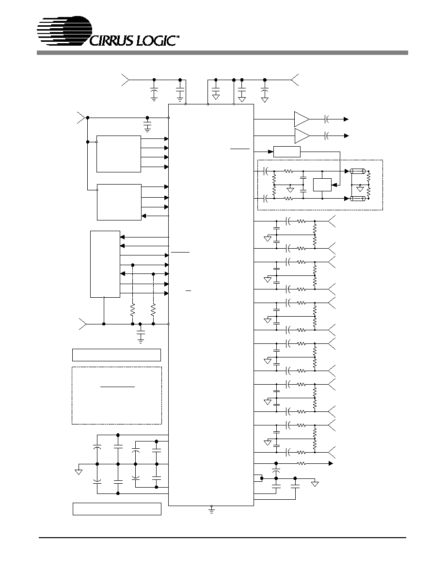
Figure 12. Typical Connection Diagram

CS4245
29
4. APPLICATIONS
4.1
Recommended Power-Up Sequence
1)
Hold RESET low until the power supply, MCLK1, MCLK2 (if used), LRCK1 and LRCK2 are stable. In this state,
the Control Port is reset to its default settings.
2)
Bring RESET high. The device will remain in a low power state with the PDN bit set by default. The control port
will be accessible.
3)
The desired register settings can be loaded while the PDN bit remains set.
4)
Clear the PDN bit to initiate the power-up sequence.
4.2
System Clocking
The CS4245 will operate at sampling frequencies from 4 kHz to 200 kHz. This range is divided into three speed
modes as shown in Table 1 below.
The CS4245 has two serial ports which may be operated synchronously or asynchronously. Serial port 1 consists
of the SCLK1 and LRCK1 signals and clocks the serial audio output, SDOUT. Serial port 2 consists of the SCLK2
and LRCK2 signals and clocks the serial audio input, SDIN.
Each serial port may be independently placed into Single, Double, or Quad Speed mode. The serial ports may also
be independently placed into Master or Slave mode.
4.2.1
Synchronous / Asynchronous Mode
By default, the CS4245 operates in synchronous mode with both serial ports synchronous to MCLK1. In this mode,
the serial ports may operate at different synchronous rates as set by the ADC_FM and DAC_FM bits, and MCLK2
does not need to be provided (the MCLK2 pin may be left unconnected).
If the Asynch bit is set (see "Asynchronous Mode (Bit 0)" on page 43), the CS4245 will operate in asynchronous
mode. The serial ports will operate asynchronously with Serial Port 1 clocked from MCLK1 and Serial Port 2 clocked
from MCLK2. In this mode, the serial ports may operate at different asynchronous rates.
4.2.2
Master Clock
In asynchronous mode MCLK1/LRCK1 and MCLK2/LRCK2 must maintain an integer ratio. In synchronous mode
MCLK1/LRCK1 and MCLK1/LRCK2 must maintain an integer ratio. Some common ratios are shown in Table 2.The
LRCK frequency is equal to Fs, the frequency at which audio samples for each channel are clocked into or out of
the device. The ADC_FM and DAC_FM bits and the MCLK Freq bits (see page 42) configure the device to generate
the proper clocks in Master Mode and receive the proper clocks in Slave Mode. Table 2 illustrates several standard
audio sample rates and the required MCLK and LRCK frequencies.
Mode
Sampling Frequency
Single Speed
4-50 kHz
Double Speed
50-100 kHz
Quad Speed
100-200 kHz
Table 1. Speed Modes
CS4245
30
4.2.3
Master Mode
As a clock master, LRCK and SCLK will operate as outputs. The two serial ports may be independently placed into
Master or Slave mode. Each LRCK and SCLK is internally derived from its respective MCLK with LRCK equal to Fs
and SCLK equal to 64 x Fs as shown in Figure 13.
4.2.4
Slave Mode
In Slave mode, SCLK and LRCK operate as inputs. Each serial port may be independently placed into Slave mode.
The Left/Right clock signal must be equal to the sample rate, Fs. If operating in asynchronous mode, LRCK1 must
be synchronously derived from MCLK1 and LRCK2 must be synchronously derived from MCLK2. If operating in syn-
chronous mode, LRCK1, and LRCK2 must be synchronously derived from MCLK1. For more information on syn-
chronous and asynchronous modes, see "Synchronous / Asynchronous Mode" on page 29.
LRCK
(kHz)
MCLK (MHz)
64x
96x
128x
192x
256x
384x
512x
768x
1024x
32
-
-
-
-
8.1920
12.2880
16.3840
24.5760
32.7680
44.1
-
-
-
-
11.2896
16.9344
22.5792
33.8680
45.1584
48
-
-
-
-
12.2880
18.4320
24.5760
36.8640
49.1520
64
-
-
8.1920
12.2880
16.3840
24.5760
32.7680
-
-
88.2
-
-
11.2896
16.9344
22.5792
33.8680
45.1584
-
-
96
-
-
12.2880
18.4320
24.5760
36.8640
49.1520
-
-
128
8.1920
12.2880
16.3840
24.5760
32.7680
-
-
-
-
176.4
11.2896
16.9344
22.5792
33.8680
45.1584
-
-
-
-
192
12.2880
18.4320
24.5760
36.8640
49.1520
-
-
-
-
Mode
QSM
DSM
SSM
Table 2. Common Clock Frequencies
˜256
˜128
˜64
˜4
˜2
˜1
00
01
10
00
01
10
LRCK1
SCLK1
000
001
010
˜1
˜1.5
˜2
011
100
˜3
˜4
MCLK1
˜256
˜128
˜64
˜4
˜2
˜1
00
01
10
00
01
10
000
001
010
˜1
˜1.5
˜2
011
100
˜3
˜4
MCLK2
LRCK2
SCLK2
0
1
DAC_FM Bits
ADC_FM Bits
ASynch Bit
MCLK1 Freq Bits
MCLK2 Freq Bits
Figure 13. Master Mode Clocking
CS4245
31
For each serial port, the serial bit clock must be equal to 128x, 64x, 48x or 32x Fs depending on the desired speed
mode. If operating in asynchronous mode, the serial bit clock SCLK1 must be synchronously derived from MCLK1
and SCLK2 must be synchronously derived from MCLK2. If operating in synchronous mode, SCLK1, and SCLK2
must be synchronously derived from MCLK1. Refer to Table 3 for required serial bit clock to Left/Right clock ratios.
4.3
High Pass Filter and DC Offset Calibration
When using operational amplifiers in the input circuitry driving the CS4245, a small DC offset may be driven into the
A/D converter. The CS4245 includes a high pass filter after the decimator to remove any DC offset which could result
in recording a DC level, possibly yielding clicks when switching between devices in a multichannel system.
The high pass filter continuously subtracts a measure of the DC offset from the output of the decimation filter. If the
HPFFreeze bit (see page 42) is set during normal operation, the current value of the DC offset for the each channel
is frozen and this DC offset will continue to be subtracted from the conversion result. This feature makes it possible
to perform a system DC offset calibration by:
1)
Running the CS4245 with the high pass filter enabled until the filter settles. See the ADC Digital Filter Charac-
teristics section for filter settling time.
2)
Disabling the high pass filter and freezing the stored DC offset.
A system calibration performed in this way will eliminate offsets anywhere in the signal path between the calibration
point and the CS4245.
4.4
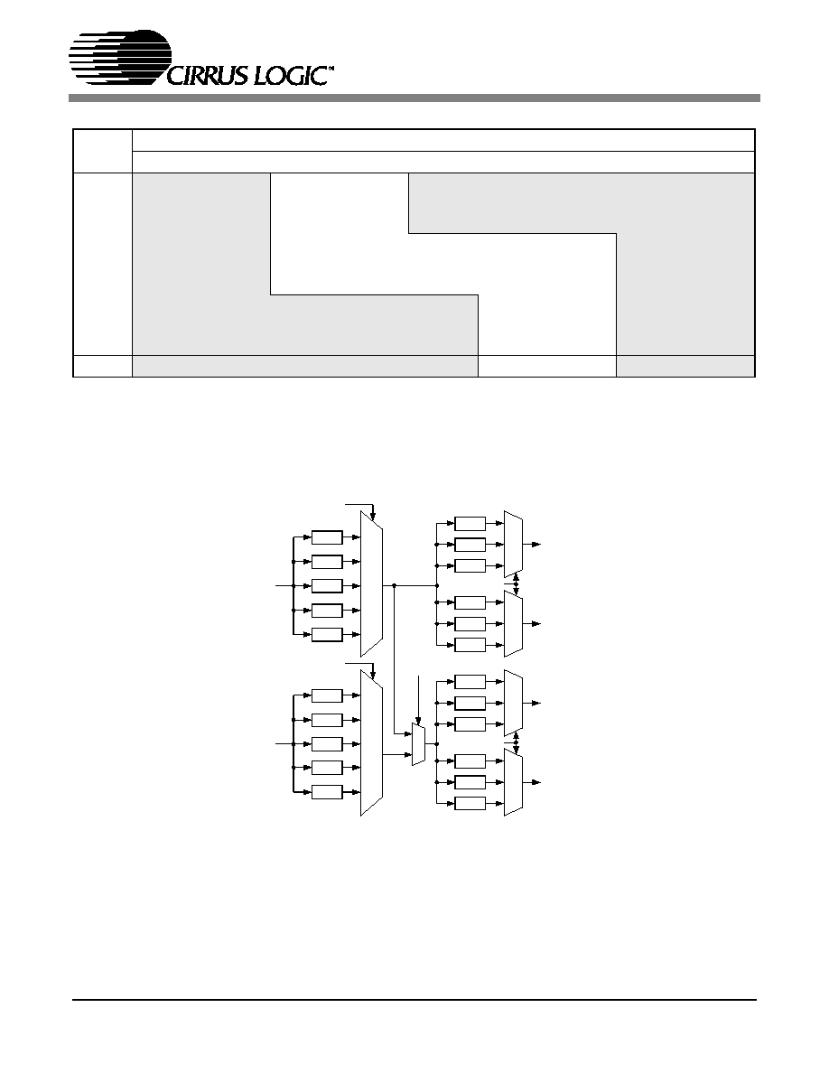
Analog Input Multiplexer, PGA, and Mic Gain
The CS4245 contains a stereo 6-to-1 analog input multiplexer followed by a programmable gain amplifier (PGA).
The input multiplexer can select one of 6 possible stereo analog input sources and route it to the PGA.
Analog inputs 4A and 4B are able to insert a +32 dB gain stage before the input multiplexer, allowing them to be
used for microphone level signals without the need for any external gain. The PGA stage provides
±12 dB of gain
or attenuation in 0.5 dB steps. Figure 14 shows the architecture of the input multiplexer, PGA, and mic gain stages.
The "Analog Input Selection (Bits 2:0)" section on page 45 outlines the bit settings necessary to control the input
multiplexer and mic gain. "Channel A PGA Control - Address 07h" on page 43 and "Channel B PGA Control - Ad-
Single Speed
Double Speed
Quad Speed
SCLK/LRCK Ratio
32x, 48x, 64x, 128x
32x, 48x, 64x
32x, 48x, 64x
Table 3. Slave Mode Serial Bit Clock Ratios
PGA
MUX
+32 dB
AIN1A
AIN2A
AIN3A
AIN4A/MICIN1
AIN5A
AIN6A
PGA
MUX
+32 dB
AIN1B
AIN2B
AIN3B
AIN4B/MICIN2
AIN5B
AIN6B
Analog Input
Selection Bits
Channel A
PGA Gain Bits
Channel B
PGA Gain Bits
Out to ADC
Channel A
Out to ADC
Channel B
Figure 14. Analog Input Architecture

CS4245
32
dress 08h" on page 44 outlines the register settings necessary to control the PGA. By default, line level input 1 is
selected, and the PGA is set to 0 dB.
4.5
Input Connections
The analog modulator samples the input at 6.144 MHz (MCLK=12.288 MHz). The digital filter will reject signals with-
in the stopband of the filter. However, there is no rejection for input signals which are (n
◊
6.144 MHz) the digital
passband frequency, where n=0,1,2,... Refer to the Typical Connection Diagram for the recommended analog input
circuit that will attenuate noise energy at 6.144 MHz. The use of capacitors which have a large voltage coefficient
(such as general purpose ceramics) must be avoided since these can degrade signal linearity. Any unused analog
input pairs should be left unconnected.
4.6
Output Connections
The CS4245 DAC's implement a switched-capacitor filter followed by a continuous time low pass filter. Its response,
combined with that of the digital interpolator, is shown in the "DAC Filter Plots" section beginning on page 50. The
recommended external analog circuitry is shown in the Typical Connection Diagram.
The CS4245 DAC is a linear phase design and does not include phase or amplitude compensation for an external
filter. Therefore, the DAC system phase and amplitude response will be dependent on the external analog circuitry.
4.7
Output Transient Control
The CS4245 uses Popguard
TM
technology to minimize the effects of output transients during power-up and power-
down. This technique eliminates the audio transients commonly produced by single-ended single-supply converters
when it is implemented with external DC-blocking capacitors connected in series with the audio outputs. To make
best use of this feature, it is necessary to understand its operation.
4.7.1
Power-up
When the device is initially powered-up, the audio outputs AOUTA and AOUTB are clamped to VQ2 which is initially
low. After the PDN bit is released (set to `0') the DAC outputs begin to ramp with VQ2 towards the nominal quiescent
voltage. This ramp takes approximately 200 ms to complete. The gradual voltage ramping allows time for the exter-
nal DC-blocking capacitors to charge to VQ2, effectively blocking the quiescent DC voltage. Audio output will begin
after approximately 2000 sample periods.
4.7.2
Power-down
To prevent audio transients at power-down the DC-blocking capacitors must fully discharge before turning off the
power. In order to do this either the PDN bit should be set or the device should be reset about 250 ms before remov-
ing power. During this time, the voltage on VQ2 and the DAC outputs discharge gradually to GND. If power is re-
moved before this 250 ms time period has passed a transient will occur when the VA supply drops below that of
VQ2. There is no minimum time for a power cycle, power may be re-applied at any time.
4.7.3
Serial Interface Clock Changes
When changing the DAC clock ratio or sample rate it is recommended that zero data (or near zero data) be present
on SDIN for at least 10 LRCK samples before the change is made. During the clocking change the DAC outputs will
always be in a zero data state. If non-zero serial audio input is present at the time of switching, a slight click or pop
may be heard as the DAC output automatically goes to it's zero data state.
4.8
Auxiliary Analog Output
The CS4245 includes an auxiliary analog output through the AUXOUT pins. These pins can be configured to output
the analog input to the ADC as selected with the input MUX and gained or attenuated with the PGA, the analog out-
put of the DAC, or alternatively they may be set to high-impedance. See the "Auxiliary Output Source Select (Bits
6:5)" section on page 43 for information on configuring the auxiliary analog output.
CS4245
33
The auxiliary analog output can source very little current. As current from the AUXOUT pins increases, distortion will
increase. For this reason, a high input impedance buffer must be used on the AUXOUT pins to achieve full perfor-
mance. Refer to the Auxiliary Output Analog Characteristics table on page 18 for acceptable loading conditions.
4.9
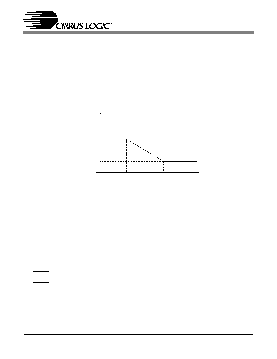
De-Emphasis Filter
The CS4245 includes on-chip digital de-emphasis optimized for a sample rate of 44.1 kHz. The filter response is
shown in Figure 15. The frequency response of the de-emphasis curve will scale proportionally with changes in sam-
ple rate, Fs. Please see section 6.3.4 for de-emphasis control.
The de-emphasis feature is included to accommodate audio recordings that utilize 50/15
µs pre-emphasis equaliza-
tion as a means of noise reduction.
De-emphasis is only available in Single Speed Mode.
4.10 Internal Digital Loopback
The CS4245 supports an internal digital loopback mode in which the output of the ADC is routed to the input of the
DAC. This mode may be activated by setting the LOOP bit in the Signal Selection register (06h - See page 43). To
use this mode, the ADC and DAC must be operating at the same synchronous sample rate.
When this bit is set, the status of the DAC_DIF[1:0] bits in register 03h will be disregarded by the CS4245. Any
changes made to the DAC_DIF[1:0] bits while the LOOP bit is set will have no impact on operation until the LOOP
bit is cleared, at which time the Digital Interface Format of the DAC will operate according to the format selected by
the DAC_DIF[1:0] bits. While the LOOP bit is set, data will be present on the SDOUT pin in the format selected by
the ADC_DIF bit in register 04h.
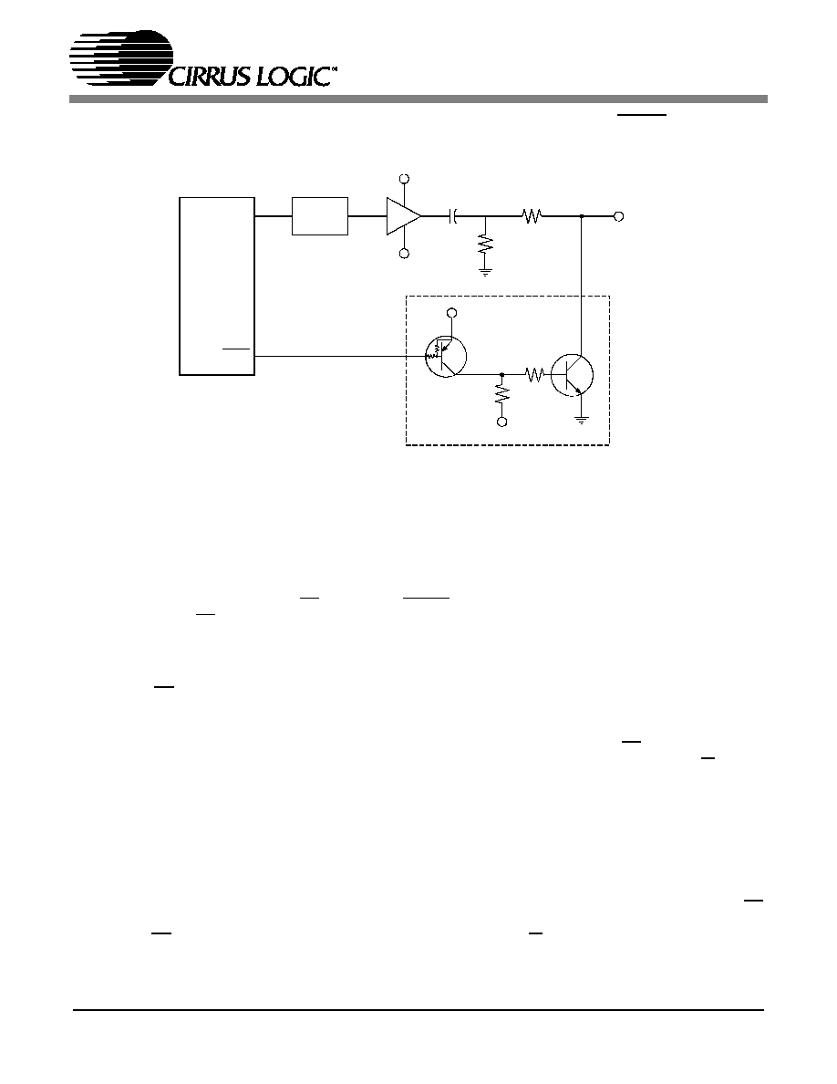
4.11 Mute Control
The MUTEC pin becomes active during power-up initialization, reset, muting, if the MCLK2 to LRCK2 ratio is incor-
rect in asynchronous mode or the MCLK1 to LRCK2 ratio is incorrect in synchronous mode, and during power-down.
The MUTEC pin is intended to be used as control for an external mute circuit in order to add off-chip mute capability.
Use of the Mute Control function is not mandatory but recommended for designs requiring the absolute minimum in
extraneous clicks and pops. Also, use of the Mute Control function can enable the system designer to achieve idle
Gain
dB
-10dB
0dB
Frequency
T2 = 15 µs
T1=50 µs
F1
F2
3.183 kHz
10.61 kHz
Figure 15. De-Emphasis Curve
CS4245
34
channel noise/signal-to-noise ratios which are only limited by the external mute circuit. The MUTEC pin is an active-
low CMOS driver. See Figure 16 below for a suggested active-low mute circuit.
4.12 Control Port Description and Timing
The control port is used to access the registers, allowing the CS4245 to be configured for the desired operational
modes and formats. The operation of the control port may be completely asynchronous with respect to the audio
sample rates. However, to avoid potential interference problems, the control port pins should remain static if no op-
eration is required.
The control port has 2 modes: SPI and I≤C, with the CS4245 acting as a slave device. SPI mode is selected if there
is a high to low transition on the AD0/CS pin, after the RESET pin has been brought high. I≤C mode is selected by
connecting the AD0/CS pin through a resistor to VLC or DGND, thereby permanently selecting the desired AD0 bit
address state.
4.12.1 SPI Mode
In SPI mode, CS is the CS4245 chip select signal, CCLK is the control port bit clock (input into the CS4245 from the
microcontroller), CDIN is the input data line from the microcontroller, CDOUT is the output data line to the microcon-
troller. Data is clocked in on the rising edge of CCLK and out on the falling edge.
Figure 17 shows the operation of the control port in SPI mode. To write to a register, bring CS low. The first seven
bits on CDIN form the chip address and must be 1001111. The eighth bit is a read/write indicator (R/W), which
should be low to write. The next eight bits form the Memory Address Pointer (MAP), which is set to the address of
the register that is to be updated. The next eight bits are the data which will be placed into the register designated
by the MAP. During writes, the CDOUT output stays in the Hi-Z state. It may be externally pulled high or low with a
47 k
resistor, if desired.
There is a MAP auto increment capability, enabled by the INCR bit in the MAP register. If INCR is a zero, the MAP
will stay constant for successive read or writes. If INCR is set to a 1, the MAP will auto-increment after each byte is
read or written, allowing block reads or writes of successive registers.
To read a register, the MAP has to be set to the correct address by executing a partial write cycle which finishes (CS
high) immediately after the MAP byte. The MAP auto increment bit (INCR) may be set or not, as desired. To begin
a read, bring CS low, send out the chip address and set the read/write bit (R/W) high. The next falling edge of CCLK
LPF
+V
EE
-V
EE
560
Audio
Out
2 k
10 k
-V
EE
+V
A
MMUN2111LT1
AOUT
MUTEC
AC
Couple
47 k
Figure 16. Suggested Active-Low Mute Circuit
CS4245
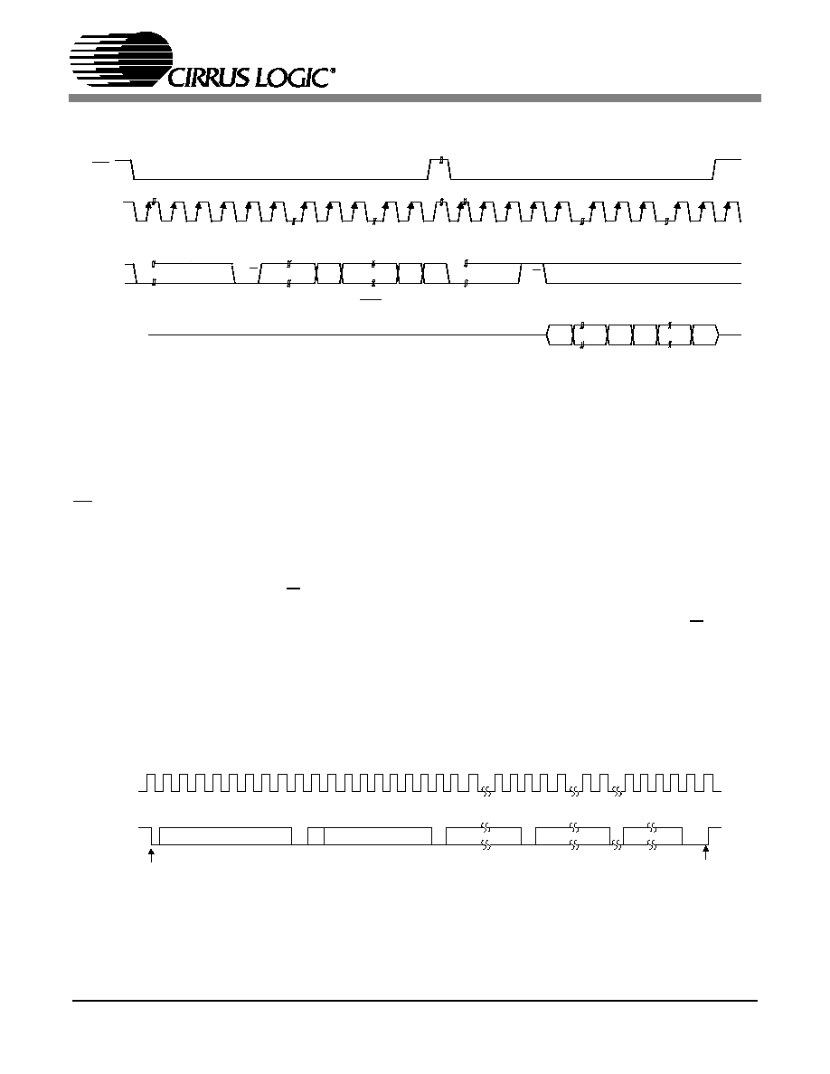
CS4245
35
will clock out the MSB of the addressed register (CDOUT will leave the high impedance state). If the MAP auto in-
crement bit is set to 1, the data for successive registers will appear consecutively.
4.12.2 I≤C Mode
In I≤C mode, SDA is a bidirectional data line. Data is clocked into and out of the part by the clock, SCL. There is no
CS pin. Pins AD0 and AD1 form the two least significant bits of the chip address and should be connected through
a resistor to VLC or DGND as desired. The state of the pins is sensed while the CS4245 is being reset.
The signal timings for a read and write cycle are shown in Figure 18 and Figure 19. A Start condition is defined as
a falling transition of SDA while the clock is high. A Stop condition is a rising transition while the clock is high. All
other transitions of SDA occur while the clock is low. The first byte sent to the CS4245 after a Start condition consists
of a 7 bit chip address field and a R/W bit (high for a read, low for a write). The upper 5 bits of the 7-bit address field
are fixed at 10011. To communicate with a CS4245, the chip address field, which is the first byte sent to the CS4245,
should match 10011 followed by the settings of the AD1 and AD0. The eighth bit of the address is the R/W bit. If the
operation is a write, the next byte is the Memory Address Pointer (MAP) which selects the register to be read or
written. If the operation is a read, the contents of the register pointed to by the MAP will be output. Setting the auto
increment bit in MAP allows successive reads or writes of consecutive registers. Each byte is separated by an ac-
knowledge bit. The ACK bit is output from the CS4245 after each input byte is read, and is input to the CS4245 from
the microcontroller after each transmitted byte.
M A P
MSB
LSB
DATA
b y te 1
b y te n
R/W
R/W
A D D R E S S
C H IP
ADDRESS
C H IP
C D IN
C C L K
CS
C D O U T
MSB
LSB MSB
LSB
1001111
1001111
MAP = Memory Address Pointer, 8 bits, MSB first
High Impedance
Figure 17. Control Port Timing in SPI Mode
4 5 6 7
24 25
SCL
CHIP ADDRESS (WRITE)
MAP BYTE
DATA
DATA +1
START
ACK
STOP
ACK
ACK
ACK
1 0 0 1 1 AD1 AD0 0
SDA
INCR
6 5 4 3 2 1 0
7 6 1 0
7 6 1 0
7 6 1 0
0 1 2 3
8 9
12
16 17 18 19
10 11
13 14 15
27 28
26
DATA +n
Figure 18. Control Port Timing, I≤C Write
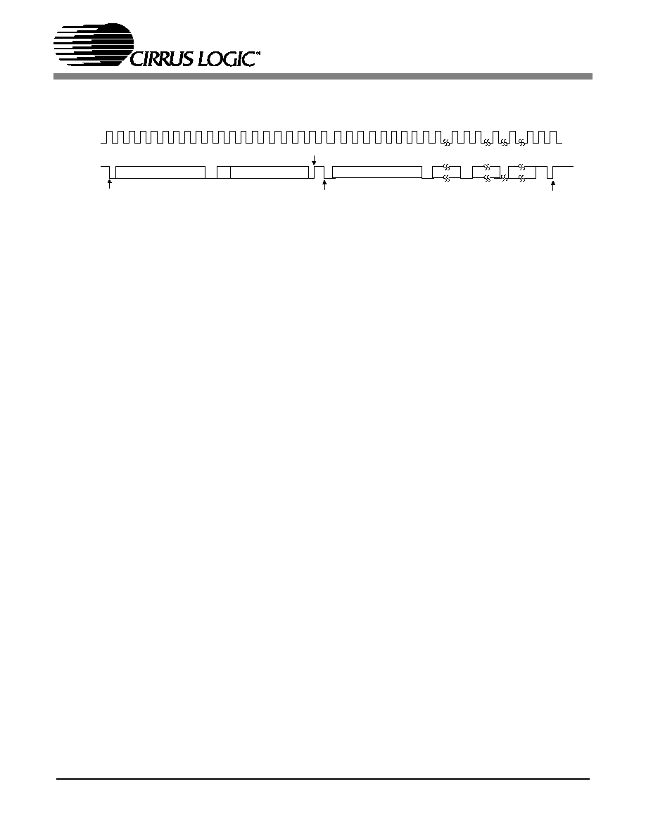
CS4245
36
Since the read operation can not set the MAP, an aborted write operation is used as a preamble. As shown in
Figure 19, the write operation is aborted after the acknowledge for the MAP byte by sending a stop condition. The
following pseudocode illustrates an aborted write operation followed by a read operation.
Send start condition.
Send 10011xx0 (chip address & write operation).
Receive acknowledge bit.
Send MAP byte, auto increment off.
Receive acknowledge bit.
Send stop condition, aborting write.
Send start condition.
Send 10011xx1(chip address & read operation).
Receive acknowledge bit.
Receive byte, contents of selected register.
Send acknowledge bit.
Send stop condition.
Setting the auto increment bit in the MAP allows successive reads or writes of consecutive registers. Each
byte is separated by an acknowledge bit.
SCL
CHIP ADDRESS (WRITE)
MAP BYTE
DATA
DATA +1
START
ACK
STOP
ACK
ACK
ACK
1 0 0 1 1 AD1 AD0 0
SDA
1 0 0 1 1 AD1 AD0 1
CHIP ADDRESS (READ)
START
INCR
6 5 4 3 2 1 0
7 0
7 0
7 0
NO
16
8 9
12 13 14 15
4 5 6 7
0 1
20 21 22 23 24
26 27 28
2 3
10 11
17 18 19
25
ACK
DATA + n
STOP
Figure 19. Control Port Timing, I≤C Read

CS4245
37
4.13 Interrupts and Overflow
The CS4245 has a comprehensive interrupt capability. The INT output pin is intended to drive the interrupt input pin
on the host microcontroller. The INT pin may function as either an active high CMOS driver or an active low open-
drain driver (see "Active High/Low (Bit 0)" on page 46). When configured as active low open-drain, the INT pin has
no active pull-up transistor, allowing it to be used for wired-OR hook-ups with multiple peripherals connected to the
microcontroller interrupt input pin. In this configuration, an external pull-up resistor must be placed on the INT pin for
proper operation.
Many conditions can cause an interrupt, as listed in the interrupt status register descriptions. See "Interrupt Status
- Address 0Dh" on page 46. Each source may be masked off through mask register bits. In addition, each source
may be set to rising edge, falling edge, or level sensitive. Combined with the option of level sensitive or edge sensi-
tive modes within the microcontroller, many different configurations are possible, depending on the needs of the
equipment designer.
The CS4245 also has a dedicated overflow output. The OVFL pin functions as active low open drain and has no
active pull-up transistor, thereby requiring an external pull-up resistor. The OVFL pin outputs an OR of the ADCOv-
erflow and ADCUnderflow conditions available in the Interrupt Status register, however, these conditions do not
need to be unmasked for proper operation of the OVFL pin.
4.14 Reset
When RESET is low, the CS4245 enters a low power mode and all internal states are reset, including the control
port and registers, and the outputs are muted. When RESET is high, the control port becomes operational and the
desired settings should be loaded into the control registers. Writing a 0 to the PDN bit in the Power Control register
will then cause the part to leave the low power state and begin operation.
The delta-sigma modulators settle in a matter of microseconds after the analog section is powered, either through
the application of power or by setting the RESET pin high. However, the voltage reference will take much longer to
reach a final value due to the presence of external capacitance on the FILT1+ and FILT2+ pins. During this voltage
reference ramp delay, both SDOUT and DAC outputs will be automatically muted.
It is recommended that RESET be activated if the analog or digital supplies drop below the recommended operating
condition to prevent power glitch related issues.
4.15 Synchronization of Multiple Devices
In systems where multiple ADCs are required, care must be taken to achieve simultaneous sampling. To ensure
synchronous sampling, the master clocks and left/right clocks must be the same for all of the CS4245's in the sys-
tem. If only one master clock source is needed, one solution is to place one CS4245 in Master Mode, and slave all
of the other CS4245's to the one master. If multiple master clock sources are needed, a possible solution would be
to supply all clocks from the same external source and time the CS4245 reset with the inactive edge of master clock.
This will ensure that all converters begin sampling on the same clock edge.
4.16 Grounding and Power Supply Decoupling
As with any high resolution converter, the CS4245 requires careful attention to power supply and grounding arrange-
ments if its potential performance is to be realized. Figure 12 shows the recommended power arrangements, with
VA connected to a clean supply. VD, which powers the digital filter, may be run from the system logic supply (VLS
or VLC) or may be powered from the analog supply (VA) via a resistor. In this case, no additional devices should be
powered from VD. Power supply decoupling capacitors should be as near to the CS4245 as possible, with the low
value ceramic capacitor being the nearest. All signals, especially clocks, should be kept away from the FILT1+,
FILT2+, VQ1 and VQ2 pins in order to avoid unwanted coupling into the modulators. The FILT1+, FILT2+, VQ1 and
VQ2 decoupling capacitors, particularly the 0.1 µF, must be positioned to minimize the electrical path from FILT1+
and FILT2+ and AGND. The CS4245 evaluation board demonstrates the optimum layout and power supply arrange-
ments. To minimize digital noise, connect the CS4245 digital outputs only to CMOS inputs.
CS4245
38
5. REGISTER QUICK REFERENCE
This table shows the register names and their associated default values.
Addr
Function
7
6
5
4
3
2
1
0
01h
Chip ID
PART3
PART2
PART1
PART0
REV3
REV2
REV1
REV0
1
1
0
0
0
0
0
1
02h
Power Control
Freeze
Reserved
Reserved
Reserved
PDN_MIC
PDN_ADC
PDN_DAC
PDN
0
0
0
0
0
0
0
1
03h
DAC Control 1
DAC_FM1 DAC_FM0 DAC_DIF1 DAC_DIF0
Reserved
MuteDAC
DeEmph
DAC_M/S
0
0
0
0
1
0
0
0
04h
ADC Control
ADC_FM1 ADC_FM0 Reserved
ADC_DIF
Reserved
MuteADC
HPFFreeze
ADC_M/S
0
0
0
0
0
0
0
0
05h
MCLK
Frequency
Reserved
MCLK1
Freq2
MCLK1
Freq1
MCLK1
Freq0
Reserved
MCLK2
Freq2
MCLK2
Freq1
MCLK2
Freq0
0
0
0
0
0
0
0
0
06h
Signal Selec-
tion
Reserved
AOutSel1
AOutSel0
Reserved
Reserved
Reserved
LOOP
ASynch
0
1
0
0
0
0
0
0
07h
PGA Ch B Gain
Control
Reserved
Reserved
Gain5
Gain4
Gain3
Gain2
Gain1
Gain0
0
0
0
0
0
0
0
0
08h
PGA Ch A Gain
Control
Reserved
Reserved
Gain5
Gain4
Gain3
Gain2
Gain1
Gain0
0
0
0
0
0
0
0
0
09h
Analog Input
Control
Reserved
Reserved
Reserved
PGASoft
PGAZero
Sel2
Sel1
Sel0
0
0
0
1
1
0
0
1
0Ah DAC Ch A Vol-
ume Control
Vol7
Vol6
Vol5
Vol4
Vol3
Vol2
Vol1
Vol0
0
0
0
0
0
0
0
0
0Bh DAC Ch B Vol-
ume Control
Vol7
Vol6
Vol5
Vol4
Vol3
Vol2
Vol1
Vol0
0
0
0
0
0
0
0
0
0Ch DAC Control 2
DACSoft
DACZero InvertDAC
Reserved
Reserved
Reserved
Reserved
Active_H/L
1
1
0
0
0
0
0
0
0Dh Interrupt Status Reserved
Reserved
Reserved
Reserved
ADCClkErr
DACClkErr
ADCOvfl
ADCUndrfl
0
0
0
0
0
0
0
0
0Eh Interrupt Mask
Reserved
Reserved
Reserved
Reserved ADCClkErrM DACClkErrM
ADCOvflM
ADCUndrflM
0
0
0
0
0
0
0
0
0Fh
Interrupt Mode
MSB
Reserved
Reserved
Reserved
Reserved ADCClkErr1 DACClkErr1
ADCOvfl1
ADCUndrfl1
0
0
0
0
0
0
0
0
10h
Interrupt Mode
LSB
Reserved
Reserved
Reserved
Reserved ADCClkErr0 DACClkErr0
ADCOvfl0
ADCUndrfl0
0
0
0
0
0
0
0
0
CS4245
39
6.
REGISTER DESCRIPTION
6.1
Chip ID - Register 01h
Function:
This register is Read-Only. Bits 7 through 4 are the part number ID which is 1100b (0Ch) and the re-
maining bits (3 through 0) are for the chip revision.
6.2
Power Control - Address 02h
6.2.1
Freeze (Bit 7)
Function:
This function allows modifications to be made to certain control port bits without the changes taking
effect until the Freeze bit is disabled. To make multiple changes to these bits take effect simulta-
neously, set the Freeze bit, make all changes, then clear the Freeze bit. The bits affected by the
Freeze function are listed in Table 4 below.
6.2.2
Power Down MIC (Bit 3)
Function:
The microphone preamplifier block will enter a low-power state whenever this bit is set.
6.2.3
Power Down ADC (Bit 2)
Function:
The ADC pair will remain in a reset state whenever this bit is set.
6.2.4
Power Down DAC (Bit 1)
Function:
The DAC pair will remain in a reset state whenever this bit is set.
6.2.5
Power Down Device (Bit 0)
Function:
The device will enter a low-power state whenever this bit is set. The power-down bit is set by default
and must be cleared before normal operation can occur. The contents of the control registers are re-
tained when the device is in power-down.
B7
B6
B5
B4
B3
B2
B1
B0
PART3
PART2
PART1
PART0
REV3
REV2
REV1
REV0
7
6
5
4
3
2
1
0
Freeze
Reserved
Reserved
Reserved
PDN_MIC
PDN_ADC
PDN_DAC
PDN
Table 4. Freeze-able Bits
Name
Register
Bit(s)
MuteDAC
03h
2
MuteADC
04h
2
Gain[5:0]
07h
5:0
Gain[5:0]
08h
5:0
Vol[7:0]
0Ah
7:0
Vol[7:0]
0Bh
7:0
CS4245
40
6.3
DAC Control - Address 03h
6.3.1
DAC Functional Mode (Bits 7:6)
Function:
Selects the required range of input sample rates.
6.3.2
DAC Digital Interface Format (Bits 5:4)
Function:
The required relationship between LRCK, SCLK and SDIN for the DAC is defined by the DAC Digital
Interface Format and the options are detailed in Table 6 and Figures 7-9.
6.3.3
Mute DAC (Bit 2)
Function:
The DAC outputs will mute and the MUTEC pin will become active when this bit is set. Though this
bit is active high, it should be noted that the MUTEC pin is active low. The common mode voltage on
the outputs will be retained when this bit is set. The muting function is effected, similar to attenuation
changes, by the DACSoft and DACZero bits in the DAC Control 2 register.
6.3.4
De-Emphasis Control (Bit 1)
Function:
The standard 50/15
µs digital de-emphasis filter response, Figure 20, may be implemented for a sam-
ple rate of 44.1 kHz when the DeEmph bit is configured as shown in Table 7 below. NOTE: De-em-
phasis is available only in Single-Speed Mode.
7
6
5
4
3
2
1
0
DAC_FM1
DAC_FM0
DAC_DIF1
DAC_DIF0
Reserved
MuteDAC
DeEmph
DAC_M/S
Table 5. Functional Mode Selection
DAC_FM1
DAC_FM0
Mode
0
0
Single-Speed Mode: 4 to 50 kHz sample rates
0
1
Double-Speed Mode: 50 to 100 kHz sample rates
1
0
Quad-Speed Mode: 100 to 200 kHz sample rates
1
1
Reserved
Table 6. DAC Digital Interface Formats
DAC_DIF1 DAC_DIF0
Description
Format
Figure
0
0
Left Justified, up to 24-bit data (default)
0
7
0
1
I
2
S, up to 24-bit data
1
8
1
0
Right Justified, 16-bit Data
2
9
1
1
Right Justified, 24-bit Data
3
9
Table 7. De-Emphasis Control
DeEmph
Description
0
Disabled (default)
1
44.1 kHz de-emphasis

CS4245
41
6.3.5
DAC Master / Slave Mode (Bit 0)
Function:
This bit selects either master or slave operation for serial audio port 2. Setting this bit will select master
mode, while clearing this bit will select slave mode.
6.4
ADC Control - Address 04h
6.4.1
ADC Functional Mode (Bits 7:6)
Function:
Selects the required range of output sample rates.
6.4.2
ADC Digital Interface Format (Bit 4)
Function:
The required relationship between LRCK1, SCLK1 and SDOUT is defined by the ADC Digital Inter-
face Format bit. The options are detailed in Table 9 and may be seen in Figure 7 and 8.
7
6
5
4
3
2
1
0
ADC_FM1
ADC_FM0
Reserved
ADC_DIF
Reserved
MuteADC
HPFFreeze
ADC_M/S
Table 8. Functional Mode Selection
ADC_FM1
ADC_FM0
Mode
0
0
Single-Speed Mode: 4 to 50 kHz sample rates
0
1
Double-Speed Mode: 50 to 100 kHz sample rates
1
0
Quad-Speed Mode: 100 to 200 kHz sample rates
1
1
Reserved
Table 9. ADC Digital Interface Formats
ADC_DIF
Description
Format
Figure
0
Left Justified, up to 24-bit data (default)
0
7
1
I
2
S, up to 24-bit data
1
8
Gain
dB
-10dB
0dB
Frequency
T2 = 15 µs
T1=50 µs
F1
F2
3.183 kHz
10.61 kHz
Figure 20. De-Emphasis Curve
CS4245
42
6.4.3
Mute ADC (Bit 2)
Function:
When this bit is set, the serial audio output of the both ADC channels will be muted.
6.4.4
ADC High Pass Filter Freeze (Bit 1)
Function:
When this bit is set, the internal high-pass filter will be disabled.The current DC offset value will be
frozen and continue to be subtracted from the conversion result. See "High Pass Filter and DC Offset
Calibration" on page 31.
6.4.5
ADC Master / Slave Mode (Bit 0)
Function:
This bit selects either master or slave operation for serial audio port 1. Setting this bit will select master
mode, while clearing this bit will select slave mode.
6.5
MCLK Frequency - Address 05h
6.5.1
Master Clock 1 Frequency (Bits 6:4)
Function:
Sets the frequency of the supplied MCLK1 signal. See Table 10 below for the appropriate settings.
6.5.2
Master Clock 2 Frequency (Bits 2:0)
Function:
Sets the frequency of the supplied MCLK2 signal. See Table 11 below for the appropriate settings.
7
6
5
4
3
2
1
0
Reserved
MCLK1
Freq2
MCLK1
Freq1
MCLK1
Freq0
Reserved
MCLK2
Freq2
MCLK2
Freq1
MCLK2
Freq0
Table 10. MCLK1 Frequency
MCLK1 Divider
MCLK1 Freq2 MCLK1 Freq1 MCLK1 Freq0
˜ 1
0
0
0
˜ 1.5
0
0
1
˜ 2
0
1
0
˜ 3
0
1
1
˜ 4
1
0
0
Reserved
1
0
1
Reserved
1
1
x
CS4245
43
6.6
Signal Selection - Address 06h
6.6.1
Auxiliary Output Source Select (Bits 6:5)
Function:
These bits are used to select the analog output source. Please refer to Table 12 below.
6.6.2
Digital Loopback (Bit 1)
Function:
When this bit is set, an internal digital loopback from the ADC to the DAC will be enabled. Please refer
to "Internal Digital Loopback" on page 33.
6.6.3
Asynchronous Mode (Bit 0)
Function:
When this bit is set, the DAC and ADC may be operated at independent an asynchronous sample
rates derived from MCLK1 and MCLK2. When this bit is cleared, the DAC and ADC must operate at
synchronous sample rates derived from MCLK1.
6.7
Channel A PGA Control - Address 07h
6.7.1
Channel A PGA Gain (Bits 5:0)
Function:
See "Channel B PGA Gain (Bits 5:0)" on page 44.
Table 11. MCLK2 Frequency
MCLK2 Divider
MCLK2 Freq2 MCLK2 Freq1 MCLK2 Freq0
˜ 1
0
0
0
˜ 1.5
0
0
1
˜ 2
0
1
0
˜ 3
0
1
1
˜ 4
1
0
0
Reserved
1
0
1
Reserved
1
1
x
7
6
5
4
3
2
1
0
Reserved
AOutSel1
AOutSel0
Reserved
Reserved
Reserved
LOOP
ASynch
Table 12. Auxiliary Output Source Selection
AOutSel1
AOutSel0
Auxiliary Output Source
0
0
High Impedance
0
1
DAC Output
1
0
PGA Output
1
1
Reserved
7
6
5
4
3
2
1
0
Reserved
Reserved
Gain5
Gain4
Gain3
Gain2
Gain1
Gain0
CS4245
44
6.8
Channel B PGA Control - Address 08h
6.8.1
Channel B PGA Gain (Bits 5:0)
Function:
Sets the gain or attenuation for the ADC input PGA stage. The gain may be adjusted from -12 dB to
+12 dB in 0.5 dB steps. The gain bits are in two's complement with the Gain0 bit set for a 0.5 dB step.
Register settings outside of the ±12 dB range are reserved and must not be used. See Table 13 for
example settings.
6.9
ADC Input Control - Address 09h
6.9.1
PGA Soft Ramp or Zero Cross Enable (Bits 4:3)
Function:
Soft Ramp Enable
Soft Ramp allows level changes, both muting and attenuation, to be implemented by incrementally
ramping, in 1/8 dB steps, from the current level to the new level at a rate of 1 dB per 8 left/right clock
periods. See Table 14 on page 45.
Zero Cross Enable
Zero Cross Enable dictates that signal level changes, either by attenuation changes or muting, will
occur on a signal zero crossing to minimize audible artifacts. The requested level change will occur
after a time-out period between 512 and 1024 sample periods (10.7 ms to 21.3 ms at 48 kHz sample
rate) if the signal does not encounter a zero crossing. The zero cross function is independently mon-
itored and implemented for each channel. See Table 14 on page 45.
Soft Ramp and Zero Cross Enable
Soft Ramp and Zero Cross Enable dictate that signal level changes, either by attenuation changes or
muting, will occur in 1/8 dB steps and be implemented on a signal zero crossing. The 1/8 dB level
change will occur after a time-out period between 512 and 1024 sample periods (10.7 ms to 21.3 ms
at 48 kHz sample rate) if the signal does not encounter a zero crossing. The zero cross function is
independently monitored and implemented for each channel. See Table 14 on page 45.
7
6
5
4
3
2
1
0
Reserved
Reserved
Gain5
Gain4
Gain3
Gain2
Gain1
Gain0
Table 13. Example Gain and Attenuation Settings
Gain[5:0]
Setting
101000
-12 dB
000000
0 dB
011000
+12 dB
7
6
5
4
3
2
1
0
Reserved
Reserved
Reserved
PGASoft
PGAZero
Sel2
Sel1
Sel0
CS4245
45
6.9.2
Analog Input Selection (Bits 2:0)
Function:
These bits are used to select the input source for the PGA and ADC. Please see Table 15 below.
6.10 DAC Channel A Volume Control - Address 0Ah
See 6.11 DAC Channel B Volume Control - Address 0Bh
6.11 DAC Channel B Volume Control - Address 0Bh
6.11.1 Volume Control (Bits 7:0)
Function:
The digital volume control allows the user to attenuate the signal in 0.5 dB increments from 0 to
-127 dB. The Vol0 bit activates a 0.5 dB attenuation when set, and no attenuation when cleared. The
Vol[7:1] bits activate attenuation equal to their decimal equivalent (in dB). Example volume settings
are decoded as shown in Table Table 16. The volume changes are implemented as dictated by the
DACSoft and DACZeroCross bits in the DAC Control 2 register (see section 6.12.1).
Table 14. PGA Soft Cross or Zero Cross Mode Selection
PGASoft
PGAZeroCross
Mode
0
0
Changes to affect immediately
0
1
Zero Cross enabled
1
0
Soft Ramp enabled
1
1
Soft Ramp and Zero Cross enabled (default)
Table 15. Analog Input Multiplexer Selection
Sel2
Sel1
Sel0
PGA/ADC Input
0
0
0
Microphone Level Inputs (+32 dB Gain Enabled)
0
0
1
Line Level Input Pair 1
0
1
0
Line Level Input Pair 2
0
1
1
Line Level Input Pair 3
1
0
0
Line Level Input Pair 4
1
0
1
Line Level Input Pair 5
1
1
0
Line Level Input Pair 6
1
1
1
Reserved
7
6
5
4
3
2
1
0
Vol7
Vol6
Vol5
Vol4
Vol3
Vol2
Vol1
Vol0
Table 16. Digital Volume Control Example Settings
Binary Code
Volume Setting
00000000
0 dB
00000001
-0.5 dB
00101000
-20 dB
00101001
-20.5 dB
11111110
-127 dB
11111111
-127.5 dB
CS4245
46
6.12 DAC Control 2 - Address 0Ch
6.12.1 DAC Soft Ramp or Zero Cross Enable (Bits 7:6)
Function:
Soft Ramp Enable
Soft Ramp allows level changes, both muting and attenuation, to be implemented by incrementally
ramping, in 1/8 dB steps, from the current level to the new level at a rate of 1 dB per 8 left/right clock
periods. See Table 17 on page 46.
Zero Cross Enable
Zero Cross Enable dictates that signal level changes, either by attenuation changes or muting, will
occur on a signal zero crossing to minimize audible artifacts. The requested level change will occur
after a time-out period between 512 and 1024 sample periods (10.7 ms to 21.3 ms at 48 kHz sample
rate) if the signal does not encounter a zero crossing. The zero cross function is independently mon-
itored and implemented for each channel. See Table 17 on page 46.
Soft Ramp and Zero Cross Enable
Soft Ramp and Zero Cross Enable dictate that signal level changes, either by attenuation changes or
muting, will occur in 1/8 dB steps and be implemented on a signal zero crossing. The 1/8 dB level
change will occur after a time-out period between 512 and 1024 sample periods (10.7 ms to 21.3 ms
at 48 kHz sample rate) if the signal does not encounter a zero crossing. The zero cross function is
independently monitored and implemented for each channel. See Table 17 on page 46.
6.12.2 Invert DAC Output (Bit 5)
Function:
When this bit is set, the output of the DAC will be inverted.
6.12.3 Active High/Low (Bit 0)
Function:
When this bit is set, the INT pin will function as an active high CMOS driver.
When this bit is cleared, the INT pin will function as an active low open drain driver and will require an
external pull-up resistor for proper operation.
6.13 Interrupt Status - Address 0Dh
For all bits in this register, a `1' means the associated interrupt condition has occurred at least once
since the register was last read. A `0' means the associated interrupt condition has NOT occurred
7
6
5
4
3
2
1
0
DACSoft
DACZero
InvertDAC
Reserved
Reserved
Reserved
Reserved
Active_H/L
Table 17. DAC Soft Cross or Zero Cross Mode Selection
DACSoft
DACZeroCross
Mode
0
0
Changes to affect immediately
0
1
Zero Cross enabled
1
0
Soft Ramp enabled
1
1
Soft Ramp and Zero Cross enabled (default)
7
6
5
4
3
2
1
0
Reserved
Reserved
Reserved
Reserved
ADCClkErr
DACClkErr
ADCOvfl
ADCUndrfl
CS4245
47
since the last reading of the register. Status bits that are masked off in the associated mask register
will always be `0' in this register. This register defaults to 00h.
6.13.1 ADC Clock Error (Bit 3)
Function:
Indicates the occurrence of an ADC clock error condition.
6.13.2 DAC Clock Error (Bit 2)
Function:
Indicates the occurrence of a DAC clock error condition.
6.13.3 ADC Overflow (Bit 1)
Function:
Indicates the occurrence of an ADC overflow condition.
6.13.4 ADC Underflow (Bit 0)
Function:
Indicates the occurrence of an ADC underflow condition.
6.14 Interrupt Mask - Address 0Eh
Function:
The bits of this register serve as a mask for the Status sources found in the register "Interrupt Status
- Address 0Dh" on page 46. If a mask bit is set to 1, the error is unmasked, meaning that its occur-
rence will affect the INT pin and the status register. If a mask bit is set to 0, the error is masked, mean-
ing that its occurrence will not affect the INT pin or the status register. The bit positions align with the
corresponding bits in the Status register.
6.15 Interrupt Mode MSB - Address 0Fh
6.16 Interrupt Mode LSB - Address 10h
Function:
The two Interrupt Mode registers form a 2-bit code for each Interrupt Status register function. There
are three ways to set the INT pin active in accordance with the interrupt condition. In the Rising edge
active mode, the INT pin becomes active on the arrival of the interrupt condition. In the Falling edge
active mode, the INT pin becomes active on the removal of the interrupt condition. In Level active
mode, the INT pin remains active during the interrupt condition.
00 - Rising edge active
01 - Falling edge active
10 - Level active
11 - Reserved
7
6
5
4
3
2
1
0
Reserved
Reserved
Reserved
Reserved
ADCClkErrM
DACClkErrM
ADCOvflM
ADCUndrflM
7
6
5
4
3
2
1
0
Reserved
Reserved
Reserved
Reserved
ADCClkErr1
DACClkErr1
ADCOvfl1
ADCUndrfl1
Reserved
Reserved
Reserved
Reserved
ADCClkErr0
DACClkErr0
ADCOvfl0
ADCUndrfl0

CS4245
48
7.
PARAMETER DEFINITIONS
Dynamic Range
The ratio of the rms value of the signal to the rms sum of all other spectral components over the specified
bandwidth. Dynamic Range is a signal-to-noise ratio measurement over the specified bandwidth made
with a -60 dBFS signal. 60 dB is added to resulting measurement to refer the measurement to full-scale.
This technique ensures that the distortion components are below the noise level and do not affect the
measurement. This measurement technique has been accepted by the Audio Engineering Society,
AES17-1991, and the Electronic Industries Association of Japan, EIAJ CP-307. Expressed in decibels.
Total Harmonic Distortion + Noise
The ratio of the rms value of the signal to the rms sum of all other spectral components over the specified
bandwidth (typically 10 Hz to 20 kHz), including distortion components. Expressed in decibels. Measured
at -1 and -20 dBFS as suggested in AES17-1991 Annex A.
Frequency Response
A measure of the amplitude response variation from 10 Hz to 20 kHz relative to the amplitude response
at 1 kHz. Units in decibels.
Interchannel Isolation
A measure of crosstalk between the left and right channels. Measured for each channel at the converter's
output with no signal to the input under test and a full-scale signal applied to the other channel. Units in
decibels.
Interchannel Gain Mismatch
The gain difference between left and right channels. Units in decibels.
Gain Error
The deviation from the nominal full-scale analog output for a full-scale digital input.
Gain Drift
The change in gain value with temperature. Units in ppm/∞C.
Offset Error
The deviation of the mid-scale transition (111...111 to 000...000) from the ideal. Units in mV.
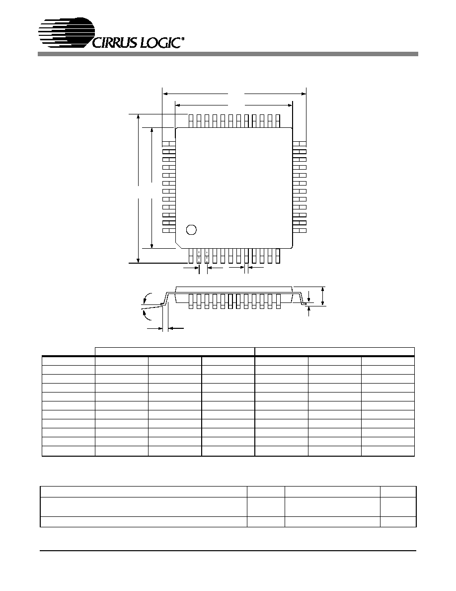
CS4245
49
8.
PACKAGE DIMENSIONS
9. THERMAL CHARACTERISTICS AND SPECIFICATIONS
Notes: 31.
JA
is specified according to JEDEC specifications for multi-layer PCBs.
INCHES
MILLIMETERS
DIM
MIN
NOM
MAX
MIN
NOM
MAX
A
---
0.055
0.063
---
1.40
1.60
A1
0.002
0.004
0.006
0.05
0.10
0.15
B
0.007
0.009
0.011
0.17
0.22
0.27
D
0.343
0.354
0.366
8.70
9.0 BSC
9.30
D1
0.272
0.28
0.280
6.90
7.0 BSC
7.10
E
0.343
0.354
0.366
8.70
9.0 BSC
9.30
E1
0.272
0.28
0.280
6.90
7.0 BSC
7.10
e*
0.016
0.020
0.024
0.40
0.50 BSC
0.60
L
0.018
0.24
0.030
0.45
0.60
0.75
0.000∞
4∞
7.000∞
0.00∞
4∞
7.00∞
* Nominal pin pitch is 0.50 mm
*Controlling dimension is mm.
*JEDEC Designation: MS022
Parameters
Symbol
Min
Typ
Max
Units
Package Thermal Resistance (Note 31)
48-LQFP
JA
JC
-
-
48
15
-
-
∞C/Watt
∞C/Watt
Allowable Junction Temperature
-
-
125
∞C
48L LQFP PACKAGE DRAWING
E1
E
D1
D
1
e
L
B
A1
A
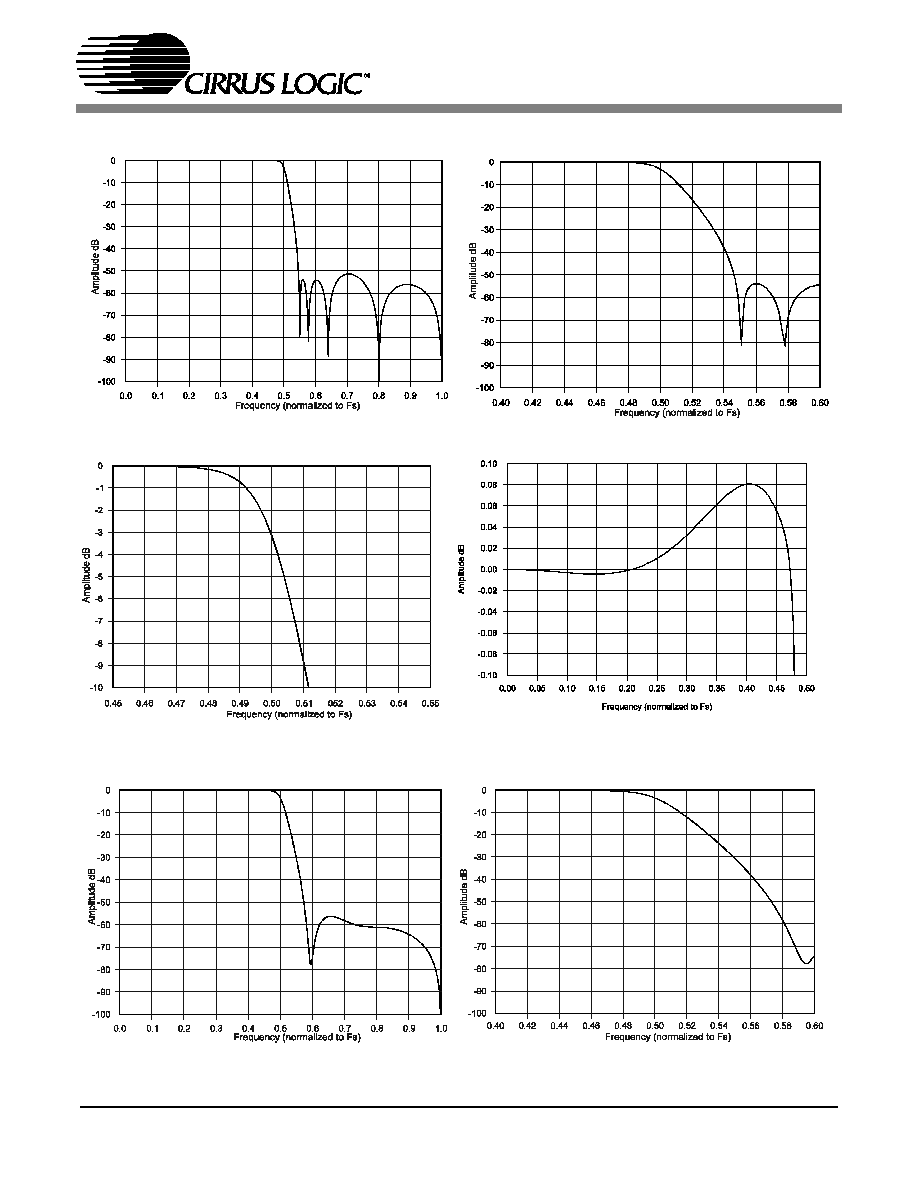
CS4245
50
APPENDIX A: DAC FILTER PLOTS
Figure 21. DAC Single Speed Stopband Rejection
Figure 22. DAC Single Speed Transition Band
Figure 23. DAC Single Speed Transition Band
Figure 24. DAC Single Speed Passband Ripple
Figure 25. DAC Double Speed Stopband Rejection
Figure 26. DAC Double Speed Transition Band
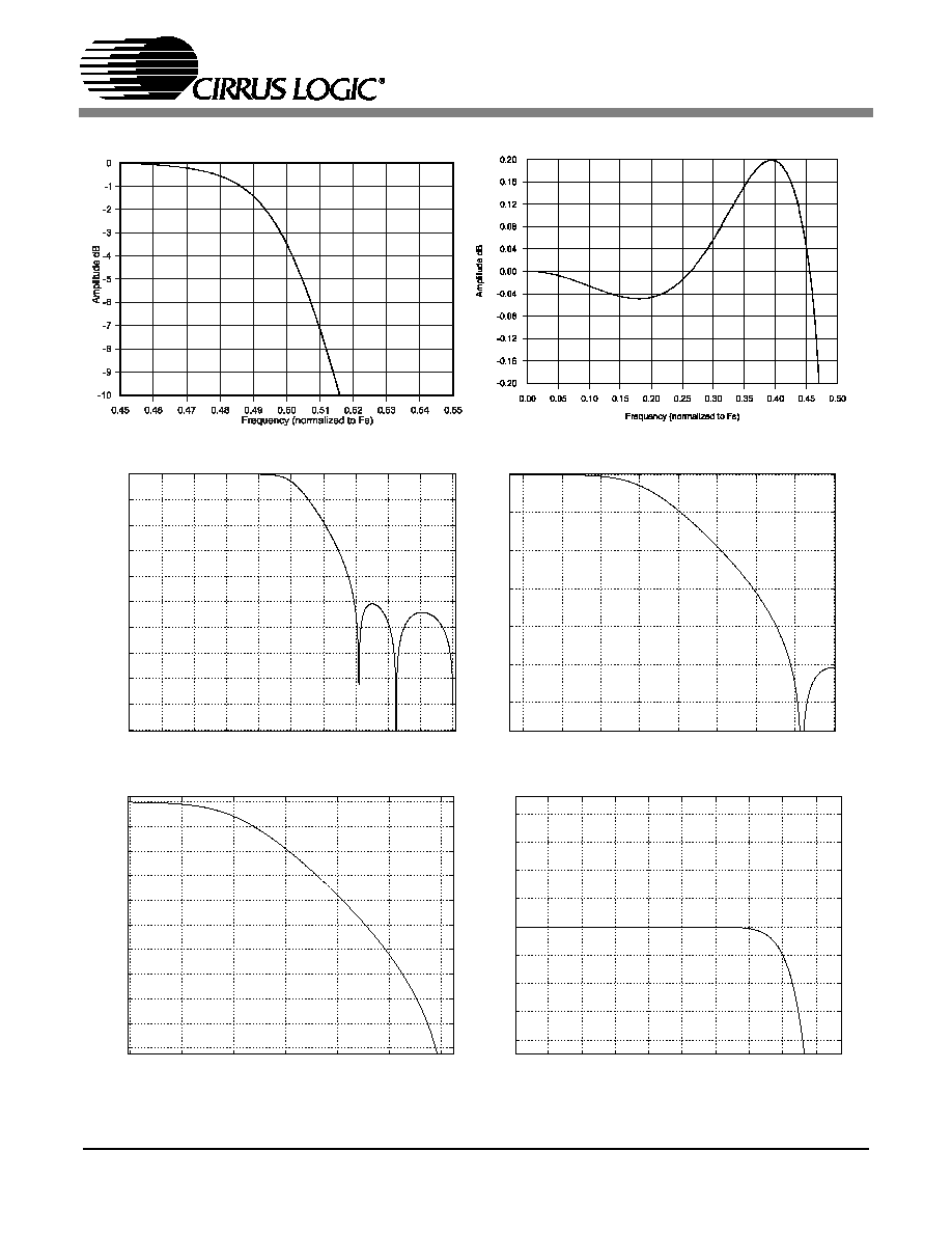
CS4245
51
Figure 27. DAC Double Speed Transition Band
Figure 28. DAC Double Speed Passband Ripple
Figure 29. DAC Quad Speed Stopband Rejection
Figure 30. DAC Quad Speed Transition Band
0.35
0.4
0.45
0.5
0.55
0.6
0.65
0.7
0.75
-60
-50
-40
-30
-20
-10
0
Amplitude (dB)
Frequency(normalized to Fs)
0
0.1
0.2
0.3
0.4
0.5
0.6
0.7
0.8
0.9
1
-100
-90
-80
-70
-60
-50
-40
-30
-20
-10
0
Amplitude (dB)
Frequency(normalized to Fs)
0.05
0.1
0.15
0.2
0.25
0.3
0.35
0.4
0.45
-0.2
-0.15
-0.1
-0.05
0
0.05
0.1
0.15
0.2
Amplitude (dB)
Frequency(normalized to Fs)
Figure 31. DAC Quad Speed Transition Band
Figure 32. DAC Quad Speed Passband Ripple
0.4
0.45
0.5
0.55
0.6
0.65
0.7
-50
-45
-40
-35
-30
-25
-20
-15
-10
-5
0
Amplitude (dB)
Frequency(normalized to Fs)
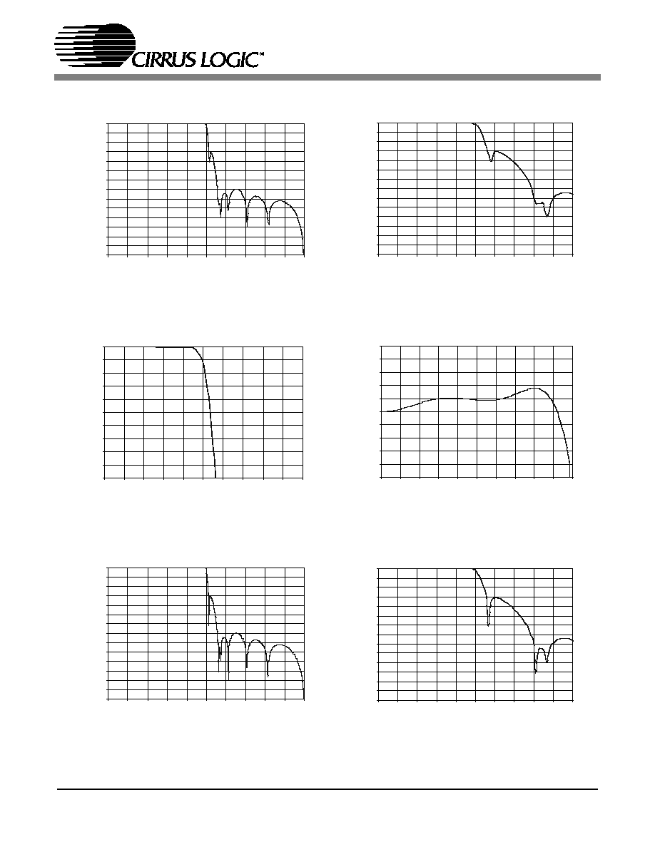
CS4245
52
APPENDIX B: ADC FILTER PLOTS
Figure 33. ADC Single Speed Stopband Rejection
Figure 34. ADC Single Speed Stopband Rejection
Figure 35. ADC Single Speed Transition Band (Detail)
Figure 36. ADC Single Speed Passband Ripple
Figure 37. ADC Double Speed Stopband Rejection
Figure 38. ADC Double Speed Stopband Rejection
-140
-130
-120
-110
-100
-90
-80
-70
-60
-50
-40
-30
-20
-10
0
0.0
0.1
0.2
0.3
0.4
0.5
0.6
0.7
0.8
0.9
1.0
Frequency (norm alized to Fs)
A
m
pl
i
t
ude (
d
B
)
-140
-130
-120
-110
-100
-90
-80
-70
-60
-50
-40
-30
-20
-10
0
0.40
0.42
0.44
0.46 0.48 0.50
0.52
0.54
0.56
0.58
0.60
Frequency (norm alized to Fs)
A
m
pl
i
t
ude (
d
B
)
-10
-9
-8
-7
-6
-5
-4
-3
-2
-1
0
0.45
0.46 0.47
0.48
0.49
0.5
0.51
0.52
0.53
0.54
0.55
Frequency (norm alized to Fs)
A
m
pl
i
t
ude (
d
B
)
-0.10
-0.08
-0.06
-0.04
-0.02
0.00
0.02
0.04
0.06
0.08
0.10
0
0.05
0.1
0.15
0.2
0.25
0.3
0.35
0.4
0.45
0.5
Frequency (norm alized to Fs)
A
m
pl
i
t
ude (
d
B
)
-140
-130
-120
-110
-100
-90
-80
-70
-60
-50
-40
-30
-20
-10
0
0.0
0.1
0.2
0.3
0.4
0.5
0.6
0.7
0.8
0.9
1.0
Frequency (norm alized to Fs)
A
m
pl
i
t
ude (
d
B
)
-140
-130
-120
-110
-100
-90
-80
-70
-60
-50
-40
-30
-20
-10
0
0.40
0.42
0.44
0.46 0.48 0.50
0.52
0.54
0.56
0.58
0.60
Frequency (norm alized to Fs)
A
m
pl
i
t
ude (
d
B
)
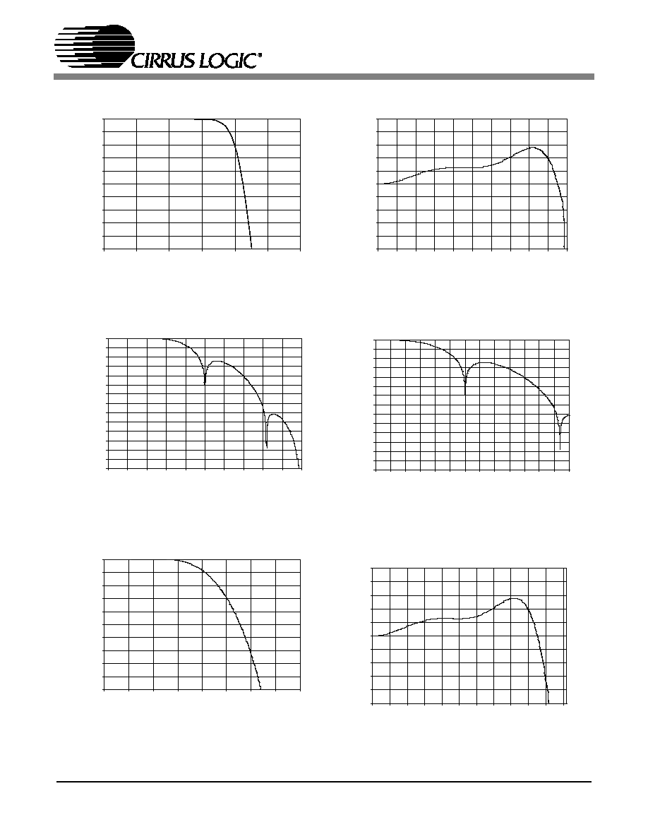
CS4245
53
Figure 39. ADC Double Speed Transition Band (De-
tail)
Figure 40. ADC Double Speed Passband Ripple
Figure 41. ADC Quad Speed Stopband Rejection
Figure 42. ADC Quad Speed Stopband Rejection
Figure 43. ADC Quad Speed Transition Band (Detail)
Figure 44. ADC Quad Speed Passband Ripple
-10
-9
-8
-7
-6
-5
-4
-3
-2
-1
0
0.46
0.47
0.48
0.49
0.50
0.51
0.52
Frequency (norm alized to Fs)
A
m
pl
i
t
ude (
d
B
)
-0.10
-0.08
-0.06
-0.04
-0.02
0.00
0.02
0.04
0.06
0.08
0.10
0.00 0.05
0.10
0.15
0.20
0.25
0.30
0.35 0.40
0.45
0.50
Frequency (norm alized to Fs)
A
m
pl
i
t
ude (
d
B
)
-140
-130
-120
-110
-100
-90
-80
-70
-60
-50
-40
-30
-20
-10
0
0.0
0.1
0.2
0.3
0.4
0.5
0.6
0.7
0.8
0.9
1.0
Frequency (norm alized to Fs)
A
m
pl
i
t
ude (
d
B
)
-140
-130
-120
-110
-100
-90
-80
-70
-60
-50
-40
-30
-20
-10
0
0.20 0.25 0.30 0.35 0.40 0.45 0.50 0.55 0.60 0.65 0.70 0.75 0.80 0.85
Frequency (norm alized to Fs)
A
m
pl
i
t
ude (
d
B
)
-10
-9
-8
-7
-6
-5
-4
-3
-2
-1
0
0.10
0.15
0.20
0.25
0.30
0.35
0.40
0.45
0.50
Frequency (norm alized to Fs)
A
m
pl
i
t
ude (
d
B
)
-0.10
-0.08
-0.06
-0.04
-0.02
0.00
0.02
0.04
0.06
0.08
0.10
0.00 0.03 0.05 0.08 0.10
0.13 0.15 0.18 0.20 0.23 0.25 0.28
Frequency (norm alized to Fs)
A
m
pl
i
t
ude (
d
B
)
CS4245
54
Release
Date
Changes
A1
May 2004
Initial Advance Release.
PP1
August 2004
Preliminary Release.
≠ Updated the VA power-down mode supply current specification on
page 19.
Table 18. Revision History
Contacting Cirrus Logic Support
For all product questions and inquiries contact a Cirrus Logic Sales Representative.
To find the one nearest to you go to
www.cirrus.com
IMPORTANT NOTICE
"Preliminary" product information describes products that are in production, but for which full characterization data is not available. Cirrus Logic, Inc. and its sub-
sidiaries ("Cirrus") believe that the information contained in this document is accurate and reliable. However, the information is subject to change without notice and
is provided "AS IS" without warranty of any kind (express or implied). Customers are advised to obtain the latest version of relevant information to verify, before
placing orders, that information being relied on is current and complete. All products are sold subject to the terms and conditions of sale supplied at the time of
order acknowledgment, including those pertaining to warranty, patent infringement, and limitation of liability. No responsibility is assumed by Cirrus for the use of
this information, including use of this information as the basis for manufacture or sale of any items, or for infringement of patents or other rights of third parties. This
document is the property of Cirrus and by furnishing this information, Cirrus grants no license, express or implied under any patents, mask work rights, copyrights,
trademarks, trade secrets or other intellectual property rights. Cirrus owns the copyrights associated with the information contained herein and gives consent for
copies to be made of the information only for use within your organization with respect to Cirrus integrated circuits or other products of Cirrus. This consent does
not extend to other copying such as copying for general distribution, advertising or promotional purposes, or for creating any work for resale.
CERTAIN APPLICATIONS USING SEMICONDUCTOR PRODUCTS MAY INVOLVE POTENTIAL RISKS OF DEATH, PERSONAL INJURY, OR SEVERE PROP-
ERTY OR ENVIRONMENTAL DAMAGE ("CRITICAL APPLICATIONS"). CIRRUS PRODUCTS ARE NOT DESIGNED, AUTHORIZED OR WARRANTED FOR
USE IN AIRCRAFT SYSTEMS, MILITARY APPLICATIONS, PRODUCTS SURGICALLY IMPLANTED INTO THE BODY, LIFE SUPPORT PRODUCTS OR OTH-
ER CRITICAL APPLICATIONS (INCLUDING MEDICAL DEVICES, AIRCRAFT SYSTEMS OR COMPONENTS AND PERSONAL OR AUTOMOTIVE SAFETY OR
SECURITY DEVICES). INCLUSION OF CIRRUS PRODUCTS IN SUCH APPLICATIONS IS UNDERSTOOD TO BE FULLY AT THE CUSTOMER'S RISK AND
CIRRUS DISCLAIMS AND MAKES NO WARRANTY, EXPRESS, STATUTORY OR IMPLIED, INCLUDING THE IMPLIED WARRANTIES OF MERCHANTABIL-
ITY AND FITNESS FOR PARTICULAR PURPOSE, WITH REGARD TO ANY CIRRUS PRODUCT THAT IS USED IN SUCH A MANNER. IF THE CUSTOMER
OR CUSTOMER'S CUSTOMER USES OR PERMITS THE USE OF CIRRUS PRODUCTS IN CRITICAL APPLICATIONS, CUSTOMER AGREES, BY SUCH USE,
TO FULLY INDEMNIFY CIRRUS, ITS OFFICERS, DIRECTORS, EMPLOYEES, DISTRIBUTORS AND OTHER AGENTS FROM ANY AND ALL LIABILITY, IN-
CLUDING ATTORNEYS' FEES AND COSTS, THAT MAY RESULT FROM OR ARISE IN CONNECTION WITH THESE USES.
Cirrus Logic, Cirrus, the Cirrus Logic logo designs, and Popguard are trademarks of Cirrus Logic, Inc. All other brand and product names in this document may be
trademarks or service marks of their respective owners.
I2C is a registered trademark of Philips Semiconductor. Purchase of I2C Components of Cirrus Logic, Inc., or one of its sublicensed Associated Companies conveys
a license under the Philips I2C Patent Rights to use those components in a standard I2C system.