 | –≠–ї–µ–Ї—В—А–Њ–љ–љ—Л–є –Ї–Њ–Љ–њ–Њ–љ–µ–љ—В: CS4265 | –°–Ї–∞—З–∞—В—М:  PDF PDF  ZIP ZIP |

Advance Product Information
This document contains information for a new product.
Cirrus Logic reserves the right to modify this product without notice.
1
Copyright
©
Cirrus Logic, Inc. 2004
(All Rights Reserved)
Cirrus Logic, Inc.
www.cirrus.com
CS4265
105 dB, 24-Bit, 192 kHz Stereo Audio CODEC
NOV `04
DS657A2
D/A Features
Multi-bit Delta Sigma modulator
105 dB Dynamic Range
-95 dB THD+N
Up to 192 kHz Sampling Rates
Single-ended Analog Architecture
Volume Control with Soft Ramp
≠ 0.5 dB Step Size
≠ Zero Crossing Click-free Transitions
Popguard
TM
Technology
≠ Minimizes the effects of output transients.
Filtered Line-level Outputs
Selectable Serial Audio Interface Formats
≠ Left Justified up to 24-bit
≠ I
2
S up to 24-bit
≠ Right Justified 16, 18, 20 and 24-bit
Selectable 50/15
µ
s De-emphasis
A/D Features
Multi-bit Delta Sigma Modulator
105 dB Dynamic Range
-95 dB THD+N
Stereo 2:1 Input Multiplexer
Programmable Gain Amplifier (PGA)
≠ +/- 12 dB gain, 0.5 dB Step Size
≠ Zero Crossing, Click-free Transitions
Pseudo-differential Stereo Line Inputs
Stereo Microphone Inputs
≠ +32 dB Gain Stage
≠ Low-noise Bias Supply
Up to 192 kHz Sampling Rates
Selectable Serial Audio Interface Formats
≠ Left Justified up to 24-bit
≠ I≤S up to 24-bit
High-pass Filter or DC Offset Calibration
1 .8 V to 5 V
M u ltib it
M o d u la to r
M u ltib it
M o d u la to r
L in e a r P h a s e
A n ti-A lia s F ilte r
In te rp o la tio n
F ilte r
In te rp o la tio n
F ilte r
L e ft D A C O u tp u t
R ig h t D A C O u tp u t
S w itc h e d C a p a c ito r
D A C a n d F ilte r
M u ltib it
O v e rs a m p lin g
A D C
M u ltib it
O v e rs a m p lin g
A D C
L in e a r P h a s e
A n ti-A lia s F ilte r
H ig h P a s s
F ilte r
H ig h P a s s
F ilte r
S te re o
L in e In p u t
S e ria l
A u d io
In p u t
S e ria l
A u d io
O u tp u t
3 .3 V to 5 V
3 .3 V to 5 V
S w itc h e d C a p a c ito r
D A C a n d F ilte r
M U X
P G A
V o lu m e
C o n tro l
V o lu m e
C o n tro l
P
C
M
S
e
r
i
a
l
In
te
r
f
a
c
e
/ L
o
o
p
b
a
c
k
M u te
C o n tro l
L
e
v
e
l
Tr
an
s
l
at
o
r
L
e
ve
l
T
r
a
n
sl
a
t
o
r
R e s e t
I
2
C C o n tro l
D a ta
M u te C o n tro l
M ic In p u t
1 & 2
P G A
+ 3 2 d B
+ 3 2 d B
In te rn a l V o lta g e
R e fe re n c e
IE C 6 0 9 5 8 -3 T ra n s m itte r
M ic B ia s
M ic ro p h o n e B ia s
T ra n s m itte r O u tp u t
R
e
g
i
s
t
e
r
C
o
nf
i
g
ur
a
t
i
o
n

CS4265
2
DS657A2
System Features
Synchronous IEC60958-3 Transmitter
≠ Up to 192 kHz Sampling Rates
≠ 75
Drive Capability
Serial Audio Data Input Multiplexer
Internal Digital Loopback
Supports Master or Slave Operation
Mute Output Control
Power Down Mode
≠ Available for A/D, D/A, CODEC, Mic
Preamplifier
+3.3 V to +5 V Analog Power Supply
+3.3 V to +5 V digital Power Supply
Direct Interface with 1.8 V to 5 V Logic
Levels
Supports I≤C Control Port Interface
General Description
The CS4265 is a highly integrated stereo audio CO-
DEC. The CS4265 performs stereo analog-to-digital
(A/D) and digital-to-analog (D/A) conversion of up to
24-bit serial values at sample rates up to 192 kHz.
A 2:1 stereo input multiplexer is included for selecting
between line level or microphone level inputs. The mi-
crophone input path includes a +32 dB gain stage and a
low noise bias voltage supply. The PGA is available for
line or microphone inputs and provides gain or attenua-
tion of
±
12 dB in 0.5 dB steps.
The output of the PGA is followed by an advanced 5th-
order, multi-bit delta sigma modulator and digital filter-
ing/decimation. Sampled data is transmitted by the
serial audio interface at rates from 4 kHz to 192 kHz in
either slave or master mode.
The D/A converter is based on a 4th-order multi-bit delta
sigma modulator with an ultra-linear low pass filter and
offers a volume control that operates with a 0.5 dB step
size. It incorporates selectable soft ramp and zero
crossing transition functions to eliminate clicks and
pops.
Standard 50/15
µ
s de-emphasis is available for a
44.1 kHz sample rate for compatibility with digital audio
programs mastered using the 50/15
µ
s pre-emphasis
technique.
Integrated level translators allow easy interfacing be-
tween the CS4265 and other devices operating over a
wide range of logic levels.
ORDERING INFORMATION
CS4265-CNZ, Lead Free
-10∞ to 70∞ C 32-pin QFN
CDB4265
Evaluation Board

CS4265
DS657A2
3
TABLE OF CONTENTS
1. PIN DESCRIPTIONS ............................................................................................................... 5
2. CHARACTERISTICS AND SPECIFICATIONS ....................................................................... 7
SPECIFIED OPERATING CONDITIONS................................................................................. 7
ABSOLUTE MAXIMUM RATINGS ........................................................................................... 7
DAC ANALOG CHARACTERISTICS ....................................................................................... 8
DAC COMBINED INTERPOLATION & ON-CHIP ANALOG FILTER RESPONSE.................. 9
ADC ANALOG CHARACTERISTICS ..................................................................................... 11
ADC ANALOG CHARACTERISTICS ..................................................................................... 13
ADC DIGITAL FILTER CHARACTERISTICS......................................................................... 14
DC ELECTRICAL CHARACTERISTICS ................................................................................ 15
DIGITAL INTERFACE CHARACTERISTICS ......................................................................... 16
SWITCHING CHARACTERISTICS - SERIAL AUDIO PORT................................................. 17
SWITCHING CHARACTERISTICS - I≤C CONTROL PORT................................................... 20
3. TYPICAL CONNECTION DIAGRAM .................................................................................... 21
4. APPLICATIONS .................................................................................................................... 22
4.1 Recommended Power-Up Sequence ............................................................................. 22
4.2 System Clocking ............................................................................................................. 22
4.2.1 Master Clock ...................................................................................................... 22
4.2.2 Master Mode ...................................................................................................... 23
4.2.3 Slave Mode ........................................................................................................ 23
4.3 High Pass Filter and DC Offset Calibration .................................................................... 23
4.4 Analog Input Multiplexer, PGA, and Mic Gain ................................................................ 24
4.5 Input Connections ........................................................................................................... 24
4.5.1 Pseudo-Differential Input ................................................................................... 24
4.6 Output Connections ........................................................................................................ 25
4.7 Output Transient Control ................................................................................................ 25
4.7.1 Power-up ............................................................................................................ 25
4.7.2 Power-down ....................................................................................................... 25
4.7.3 Serial Interface Clock Changes ......................................................................... 25
4.8 DAC Serial Data Input Multiplexer .................................................................................. 26
4.9 De-Emphasis Filter ......................................................................................................... 26
4.10 Internal Digital Loopback .............................................................................................. 26
4.11 Mute Control ................................................................................................................. 26
4.12 AES3 Transmitter ......................................................................................................... 27
4.12.1 TxOut Driver ..................................................................................................... 27
4.12.2 Mono Mode Operation ..................................................................................... 27
4.13 I≤C Control Port Description and Timing ....................................................................... 28
4.14 Status Reporting ........................................................................................................... 29
4.15 Reset ........................................................................................................................... 29
4.16 Synchronization of Multiple Devices ............................................................................. 30
4.17 Grounding and Power Supply Decoupling .................................................................... 30
4.18 Package Considerations ............................................................................................... 30
5. REGISTER QUICK REFERENCE ......................................................................................... 31
6. REGISTER DESCRIPTION ................................................................................................... 33
6.1 Chip ID - Register 01h .................................................................................................... 33
6.2 Power Control - Address 02h ......................................................................................... 33
6.3 DAC Control - Address 03h ............................................................................................ 34
6.4 ADC Control - Address 04h ............................................................................................ 34
6.5 MCLK Frequency - Address 05h .................................................................................... 36
6.6 Signal Selection - Address 06h ...................................................................................... 36
6.7 Channel A PGA Control - Address 07h .......................................................................... 36
6.8 Channel B PGA Control - Address 08h .......................................................................... 37

CS4265
4
DS657A2
6.9 ADC Input Control - Address 09h ................................................................................... 37
6.10 DAC Channel A Volume Control - Address 0Ah ........................................................... 38
6.11 DAC Channel B Volume Control - Address 0Bh ........................................................... 38
6.12 DAC Control 2 - Address 0Ch ....................................................................................... 38
6.13 Status - Address 0Dh .................................................................................................... 39
6.14 Status Mask - Address 0Eh .......................................................................................... 40
6.15 Status Mode MSB - Address 0Fh ................................................................................. 40
6.16 Status Mode LSB - Address 10h ................................................................................... 40
6.17 Transmitter Control 1 - Address 11h ............................................................................. 40
6.18 Transmitter Control 2 - Address 12h ............................................................................. 41
7. PARAMETER DEFINITIONS ................................................................................................. 43
8. PACKAGE DIMENSIONS ..................................................................................................... 44
9. THERMAL CHARACTERISTICS AND SPECIFICATIONS ................................................. 44
Appendix A: DAC Filter Plots ......................................................................................... 45
Appendix B: ADC Filter Plots .............................................................................................. 47
Appendix C: External IEC60958-3 Transmitter Components .............................................. 49
C.1 IEC60958-3 Transmitter External Components ............................................................. 49
C.2 Isolating Transformer Requirements .............................................................................. 49
Appendix D: Channel Status Buffer Management ............................................................... 50
D.1 IEC60958-3 Channel Status (C) Bit Management ......................................................... 50
D.1.1 Accessing the E buffer ....................................................................................... 50
D.1.2 Serial Copy Management System (SCMS) ....................................................... 51
D.1.3 Channel Status Data E Buffer Access ............................................................... 51
D.1.3.1 One Byte mode ................................................................................... 51
D.1.3.2 Two Byte mode ................................................................................... 51
CS4265
DS657A2
5
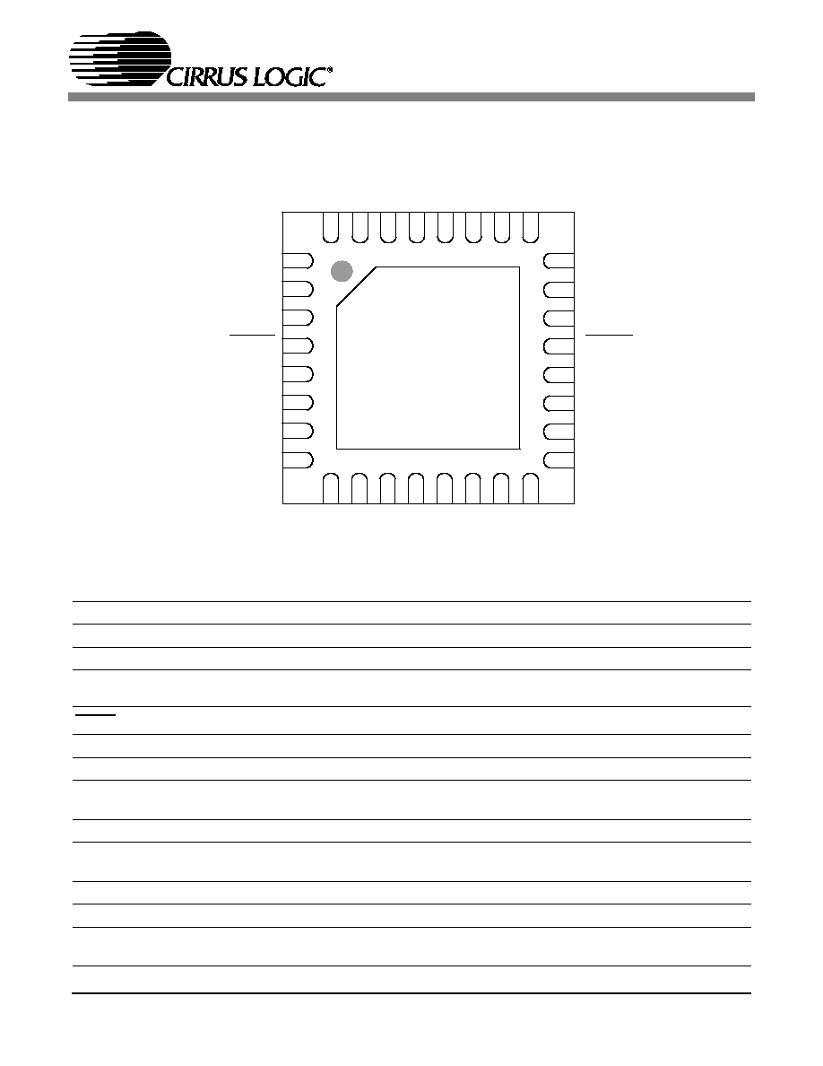
1. PIN DESCRIPTIONS
Pin Name
#
Pin Description
SDA
1
Serial Control Data (Input/Output) - Bidirectional data line for the I≤C control port.
SCL
2
Serial Control Port Clock (Input) - Serial clock for the I≤C control port.
VLC
3
Control Port Power (Input) - Determines the required signal level for the control port interface. Refer to
the Recommended Operating Conditions for appropriate voltages.
RESET
4
Reset (Input) - The device enters a low power mode when this pin is driven low.
VA
5
Analog Power (Input) - Positive power for the internal analog section.
AGND
6
Analog Ground (Input) - Ground reference for the internal analog section.
AINA
AINB
7,
8
Analog Input (Input) - The full scale level is specified in the ADC Analog Characteristics specification
table.
SGND
9
Signal Ground (Input) - Ground reference for the analog line inputs.
AFILTA
AFILTB
10,
11
Antialias Filter Connection (Output) - Antialias filter connection for the ADC inputs.
VQ
12
Quiescent Voltage (Output) - Filter connection for internal quiescent voltage.
FILT+
13
Positive Voltage Reference (Output) - Positive reference voltage for the internal sampling circuits.
MICIN1
MICIN2
14,
15
Microphone Input (Input) - The full scale level is specified in the ADC Analog Characteristics specifica-
tion table.
10
9
8
7
6
5
4
3
2
1
11
12
13
14
15
16
17
18
19
20
21
22
23
24
25
26
27
28
29
30
31
32
Top-Down (Through Package) View
32-Pin QFN Package
TXOUT
VD
DGND
MCLK
LRCK
SCLK
SDOUT
SDIN1
SGND
AFILTA
AFILTB
VQ
FI
LT
+
MICIN1
MICIN2
MICBIAS
SDA
SCL
VLC
RESET
VA
AGND
AINA
AINB
SDIN2
TXSDIN
VLS
MUTEC
AOUTB
AOUTA
AGND
VA
Thermal Pad