 | –≠–ª–µ–∫—Ç—Ä–æ–Ω–Ω—ã–π –∫–æ–º–ø–æ–Ω–µ–Ω—Ç: CS4333-BS | –°–∫–∞—á–∞—Ç—å:  PDF PDF  ZIP ZIP |

1
Copyright
©
Cirrus Logic, Inc. 1997
(All Rights Reserved)
Cirrus Logic, Inc.
Crystal Semiconductor Products Division
P.O. Box 17847, Austin, Texas 78760
(512) 445 7222 FAX: (512) 445 7581
http://www.crystal.com
CS4330/31/33
8 Pin Stereo D/A Converter for Digital Audio
Features
l
Complete Stereo DAC System:
Interpolation, D/A, Output Analog Filtering
l
18-Bit Resolution
l
94 dB Dynamic Range
l
0.003% THD
l
Low Clock Jitter Sensitivity
l
Single +3 V or +5 V Power Supply
l
Filtered Line Level Outputs
Linear Phase Filtering
l
On-Chip Digital De-emphasis
Description
The CS4330, CS4331 and CS4333 are complete, stereo
digital-to-analog output systems including interpolation,
1-bit D/A conversion and output analog filtering in an 8-
pin package. These devices differ in the serial interface
format used to input audio data.
The CS4330, CS4331 and CS4333 are based on delta-
sigma modulation, where the modulator output controls
the reference voltage input to an ultra-linear analog low-
pass filter. This architecture allows for infinite adjustment
of sample rate between 2 kHz and 50 kHz while main-
taining linear phase response simply by changing the
master clock frequency.
The CS4330, CS4331 and CS4333 contain on-chip dig-
ital de-emphasis, operate from a single +3 V or +5 V
power supply, and consume only 60mW of power with a
3 V power supply. These features make them ideal for
portable CD players and other portable playback
systems.
ORDERING INFORMATION
See page 21.
I
LRCK
3
SDATA
1
DEM/SCLK
2
MCLK
4
VA+
AOUTL
8
AOUTR
5
Serial Input
Interface
Interpolator
Interpolator
De-emphasis
Delta-Sigma
Modulator
Delta-Sigma
Modulator
DAC
DAC
Voltage Reference
Analog
Low-Pass
Filter
Analog
Low-Pass
Filter
7
AGND
6
MAY `97
DS136F1
ANALOG CHARACTERISTICS
(T
A
= 25
∞
C; Logic "1" = VA+; Logic "0" = AGND; MCLK = 12.288 MHz;
Full-Scale Output Sine Wave, 991 Hz; Input Sample Rate = 48 kHz; Input Data = 18 Bits; SCLK = 3.072 MHz;
Measurement Bandwidth is 10 Hz to 20 kHz, unweighted; unless otherwise specified. Resistive load = 20 k
, capaci-
tive load = 100 pF)
CS4330/31/33-KS
VA +5V
CS4330/31/33-KS
VA +3V
CS4330/31/33-BS
VA +5V only
Parameter
Symbol
Min
Typ
Max
Min
Typ
Max
Min
Typ
Max
Units
Specified Temperature Range
T
A
-10
to
70
-10
to
70
-40
to
+85
∞
C
Resolution
-
-
18
-
-
18
-
-
18
Bits
Dynamic Performance
Dynamic Range
(A-weighted)
90
94
-
-
89
-
88
94
-
dB
Total Harmonic Distortion
-
0.003 0.007
-
0.003
-
-
.003
.008
%
Total Harmonic Distortion + Noise
0 dB Output,
-20 dB Output,
-60 dB Output
THD+N
-
-
-
-86
-72
-32
-81
-68
-28
-
-
-
-85
-67
-27
-80
-
-
-88
-
-
-86
-72
-32
-79
-66
-26
dB
dB
dB
Deviation From Linear Phase
(Note 1)
-
±
0.5
-
-
±
0.5
-
-
±
0.5
-
deg
Passband: to 0.05 dB corner
(Note 2,3)
0
to
21.77
0
to
21.77
0
to
21.77
kHz
Frequency Response 10 Hz to 20 kHz(Note 1)
-
±
0.1
-
-
±
0.1
-
-
±
0.1
-
dB
Passband Ripple
(Note 3)
-
-
±
0.05
-
-
±
0.05
-
-
±
0.05
dB
StopBand
(Notes 2,3)
26.23
26.23
26.23
-
-
kHz
StopBand Attenuation
(Note 4)
60
-
-
60
-
-
60
-
-
dB
Group Delay (Fs = Input Sample Rate)
tgd
-
16 / Fs
-
-
16 / Fs
-
-
16 / Fs
-
s
Interchannel Isolation (1 kHz)
-
90
-
-
90
-
-
90
-
dB
dc Accuracy
Interchannel Gain Mismatch
-
0.1
-
-
0.1
-
-
0.1
-
dB
Gain Error
-
-
±
10
-
-
±
10
-
-
±
10
%
Gain Drift
-
250
-
-
250
-
-
250
-
ppm/
∞
C
Analog Output
Full Scale Output Voltage
3.33
3.70
4.07
1.66
1.85
2.03
3.33
3.70
4.07
Vpp
Output Common Mode Voltage
-
2.3
-
-
1.3
-
-
2.3
-
VDC
Minimum Resistive Load
-
10
-
-
10
-
-
20
-
k
Maximum Capacitive Load
-
100
-
-
100
-
-
100
-
pF
Power Supplies
Power Supply Current:
normal operation
power-down
IA+
IA+
-
-
28
60
32
-
-
-
20
20
25
-
-
-
28
60
32
-
mA
µ
A
Power Dissipation
normal operation
power-down
-
-
140
0.3
160
-
-
-
60
0.06
75
-
-
-
140
0.3
160
-
mW
mW
Power Supply Rejection Ratio (1 kHz)
PSRR
-
50
-
-
50
-
-
50
-
dB
Notes: 1. Combined digital and analog filter characteristics.
2. The passband and stopband edges scale with frequency. For input sample rates, Fs, other than
48 kHz, the 0.05 dB passband edge is 0.4535
◊
Fs and the stopband edge is 0.5465
◊
Fs.
3. Digital filter characteristics.
4. Measurement Bandwidth is 10 Hz to Fs (kHz)
CS4330, CS4331, CS4333
2
DS136F1
SWITCHING CHARACTERISTICS
(TA = 25
∞
C; VA+ = 2.7V - 5.5V; Inputs: Logic 0 = 0V, Logic
1 = VA+, CL = 20 pF) Switching characteristics are guaranteed by characterization.
Parameter
Symbol
Min
Typ
Max
Units
Input Sample Rate
Fs
2
-
50
kHz
LRCK Duty Cycle (External SCLK only) (Note 5)
30
50
70
%
MCLK Pulse Width High
MCLK / LRCK = 512
10
-
1000
ns
MCLK Pulse Width Low
MCLK / LRCK = 512
15
-
1000
ns
MCLK Pulse Width High
MCLK / LRCK = 384
21
-
1000
ns
MCLK Pulse Width Low
MCLK / LRCK = 384
21
-
1000
ns
MCLK Pulse Width High
MCLK / LRCK = 256
35
-
1000
ns
MCLK Pulse Width Low
MCLK / LRCK = 256
39
-
1000
ns
External SCLK Mode
SCLK Pulse Width Low
tsclkl
20
-
-
ns
SCLK Pulse Width High
tsclkh
20
-
-
ns
SCLK Period
tsclkw
1
(
128
)
Fs
-
-
ns
SCLK rising to LRCK edge delay
tslrd
20
-
-
ns
SCLK rising to LRCK edge setup time
tslrs
20
-
-
ns
SDATA valid to SCLK rising setup time
tsdlrs
20
-
-
ns
SCLK rising to SDATA hold time
tsdh
20
-
-
ns
Internal SCLK Mode
SCLK Period
(Note 6)
tsclkw
1
SCLK
-
-
ns
SCLK rising to LRCK edge
tsclkr
-
t
sclkw
2
-
µ
s
SDATA valid to SCLK rising setup time
tsdlrs
1
(
512
)
Fs
+
15
-
-
ns
SCLK rising to SDATA hold time
MCLK / LRCK = 256 or 512
tsdh
1
(
512
)
Fs
+
15
-
-
ns
SCLK rising to SDATA hold time
MCLK / LRCK = 384
tsdh
1
(
384
)
Fs
+
15
-
-
ns
Notes: 5.
In Internal SCLK Mode, the Duty Cycle must be 50%
±
1/2 MCLK Period.
6.
The SCLK / LRCK ratio may be either 32, 48, or 64.
CS4330, CS4331, CS4333
DS136F1
3

sclkh
t
slrs
t
slrd
t
sdlrs
t
sdh
t
sclkl
t
SDATA
SCLK
LRCK
External Serial Mode Input Timing
SDATA
LRCK
MCLK
*INTERNAL SCLK
1
N
2
N
Internal Serial Clock Generation
* The SCLK pulses shown are internal to the CS4330/31/33.
N equals MCLK divided by SCLK
SDATA
**INTERNAL SCLK
*LRCK
sclkw
t
sdlrs
t
sdh
t
sclkr
t
Internal Serial Mode Input Timing
* LRCK for CS4331
** The SCLK pulses shown are internal to the CS4330/31/33.
CS4330, CS4331, CS4333
4
DS136F1

RECOMMENDED OPERATING CONDITIONS
(AGND = 0V; all voltages with respect to
ground)
Parameter
Symbol
Min
Typ
Max
Units
DC Power Supply:
(3V mode)
VA+
2.7
3.0
4.0
V
(5V mode)
VA+
4.75
5.0
5.5
V
DIGITAL CHARACTERISTICS
(TA = 25
∞
C; VA+ = 2.7V - 5.5V)
Parameter
Symbol
Min
Typ
Max
Units
High-Level Input Voltage
(VA+ = 5.5V)
VIH
2.4
-
-
V
(VA+ = 5.0V)
VIH
2.0
-
-
V
Low-Level Input Voltage
VIL
-
-
0.8
V
Input Leakage Current
(Note 7)
Iin
-
-
±
10
µ
A
Notes: 7. I
in
for CS4331 LRCK is
±
20
µ
A max.
ABSOLUTE MAXIMUM RATINGS
(AGND = 0V; all voltages with respect to ground.)
Parameter
Symbol
Min
Max
Units
DC Power Supply:
VA+
-0.3
6.0
V
Input Current, Any Pin Except Supplies
Iin
-
±
10
mA
Digital Input Voltage
VIND
-0.3
(VA+)+0.4
V
Ambient Operating Temperature (power applied)
TA
-55
125
∞
C
Storage Temperature
Tstg
-65
150
∞
C
WARNING: Operation at or beyond these limits may result in permanent damage to the device.
Normal operation is not guaranteed at these extremes.
CS4330, CS4331, CS4333
DS136F1
5

DEM/SCLK
6
2.4k
Audio
Data
Processor
External Clock
MCLK
AGND
AOUTR
CS4330
CS4331
CS4333
SDATA
LRCK
VA+
AOUTL
3
1
2
4
7
0.1
µ
F
+
10
µ
F
+3V/+5V
10
µ
F
8
C
56k
Left Audio
Output
*
*
2.4k
10
µ
F
5
C
56k
Right Audio
Output
*
*
* Required for AC coupling only
**
**
** C =
1
(2
)(2400
)(Fs)(2)
+
+
Figure 1. Recommended Connection Diagram
CS4330, CS4331, CS4333
6
DS136F1
GENERAL DESCRIPTION
The CS4330, CS4331, and CS4333 are complete
stereo digital-to-analog systems including digital
interpolation, 128
◊
third-order delta-sigma digi-
tal-to-analog conversion, digital de-emphasis and
analog filtering, Figure 2. This architecture pro-
vides a high tolerance to clock jitter.
The primary purpose of using delta-sigma modu-
lation techniques is to avoid the limitations of
laser trimmed resistive digital-to-analog con-
verter architectures by using an inherently linear
1-bit digital-to-analog converter. The advantages
of a 1-bit digital-to-analog converter include:
ideal differential linearity, no distortion mecha-
nisms due to resistor matching errors and no
linearity drift over time and temperature due to
variations in resistor values.
Digital Interpolation Filter
The digital interpolation filter increases the sam-
ple rate by a factor of 32 and is followed by a 4
◊
digital sample-and-hold to effectively achieve a
128
◊
interpolation filter. This filter eliminates
images of the baseband audio signal which exist
at multiples of the input sample rate, Fs. This
allows for the selection of a less complex analog
filter based on out-of-band noise attenuation re-
quirements rather than anti-image filtering.
Following the interpolation filter, the resulting
frequency spectrum has images of the input sig-
nal at multiples of 128
◊
the input sample rate.
These images are removed by the external ana-
log filter.
Delta-Sigma Modulator
The interpolation filter is followed by a third-
order delta-sigma modulator which converts the
22-bit interpolation filter output into 1-bit data at
128
◊
.
Switched-Capacitor Filter
The delta-sigma modulator is followed by a
digital-to-analog converter which translates the
1-bit data into a series of charge packets. The
magnitude of the charge in each packet is deter-
mined by sampling of a voltage reference onto a
switched capacitor, where the polarity of each
packet is controlled by the 1-bit signal. This
technique greatly reduces the sensitivity to clock
jitter and is a major improvement over earlier
generations of 1-bit digital-to-analog converters.
Interpolator
Delta-Sigma
Modulator
DAC
Analog
Low-Pass
Filter
Analog
Output
Digital
Input
Figure 2. System Block Diagram
CS4330, CS4331, CS4333
DS136F1
7
SYSTEM DESIGN
The CS4330/31/33 accept data at standard audio
frequencies including 48 kHz, 44.1 kHz and
32 kHz. Audio data is input via the serial data
input pin (SDATA). The Left/Right Clock
(LRCK) defines the channel and delineation of
data and the Serial Clock (SCLK) clocks audio
data into the input data buffer. The CS4330,
CS4331 and CS4333 differ in the serial data for-
mat as shown in Figures 4-7. The Master Clock
(MCLK) is used to operate the digital interpola-
tion filter and the delta-sigma modulator.
Master Clock
The MCLK must be either 256
◊,
384
◊,
or 512
◊
the desired input sample rate, Fs. Fs is the fre-
quency at which words for each channel are
input to the digital-to-analog converter, and is
equal to the LRCK frequency. The MCLK to
LRCK frequency ratio is detected automatically
during the initialization sequence by counting
the number of MCLK transitions during a single
LRCK period. Internal dividers are set to gener-
ate the proper clocks for the digital filter,
delta-sigma modulator and switched-capacitor
filter. Table 1 illustrates several standard audio
sample rates and the required MCLK and LRCK
frequencies.
Serial Clock
The serial clock controls the shifting of data into
the input data buffers. The CS4330/31/33 sup-
port both external and internal serial clock
generation modes. Refer to Figures 4-7 for data
formats.
External Serial Clock Mode
The CS4330/31/33 will enter the External Serial
Clock Mode when 4 low to high transitions are
detected on the DEM/SCLK pin during any
phase of the LRCK period. When this mode is
enabled, the Internal Serial Clock Mode and de-
e mp ha si s filt er c ann ot be acc esse d. The
CS4330/31/33 must return to Power-Down to
exit this mode. Refer to Figure 8.
Internal Serial Clock Mode
In the Internal Serial Clock Mode, the serial
clock is internally derived and synchronous with
MCLK and LRCK. The SCLK/LRCK frequency
ratio is either 32, 48, or 64. Operation in this
mode is identical to operation with an external
serial clock synchronized with LRCK. This
mode allows access to the digital de-emphasis
function. Refer to Figure 8.
While the Internal Serial Clock Mode is pro-
vided to allow access to the de-emphasis filter,
the Internal Serial Clock Mode also eliminates
possible clock interference from an external
SCLK. Use of Internal Serial Clock Mode is al-
ways preferred, even when de-emphasis filtering
is not required.
De-Emphasis
The CS4330/31/33 include on-chip digital de-
emphasis. Figure 3 shows the de-emphasis curve
for Fs equal to 44.1 kHz. The frequency re-
sponse of the de-emphasis curve will scale
proportionally with changes in sample rate, Fs.
The de-emphasis filter is active (inactive) if the
DEM/SCLK pin is low (high) for 8 consecutive
falling edges of LRCK. This function is available
only in the internal serial clock mode.
LRCK
(kHz)
MCLK (MHz)
256x
384x
512x
32
8.1920
12.2880
16.3840
44.1
11.2896
16.9344
22.5792
48
12.2880
18.4320
24.5760
Table 1. Common Clock Frequencies
CS4330, CS4331, CS4333
8
DS136F1
Initialization and Power-Down
The Initialization and Power-Down sequence
flow chart is shown in Figure 8. The CS4330/31/33
enter the Power-Down mode upon initial power-
up. The interpolation filters and delta-sigma
modulators are reset, and the internal voltage ref-
erence, one-bit digital-to-analog converters and
switched-capacitor low-pass filters are powered
down. The device will remain in the Power-
Down mod e u nti l MC LK and LRCK are
presented. Once MCLK and LRCK are detected,
MCLK occurrences are counted over one LRCK
period to determine the MCLK/LRCK frequency
ratio. Power is then applied to the internal volt-
age reference and the +5 or +3 Volt power
supply mode is determined. Finally, power is
applied to the D/A converters and switched-ca-
pacitor filters, and the analog outputs will move
to approximately 2.3V (1.3V in 3V mode). This
process requires approximately 1ms plus 1024
cycles of LRCK.
The CS4330/31/33 enter the Power-Down mode
within 1 period of LRCK if either MCLK or
LRCK is removed. The initialization sequence
begins when MCLK and LRCK are restored. If
the MCLK/LRCK frequency ratio or the VA+
voltage changes during Power-Down, the
CS4330/31/33 adapt to these new operating con-
ditions. It is recomended that the CS4330/31/33
not be powered up with the clocks (MCLK,
LRCK, SCLK) going.
Power Supply Determination
The nominal power supply voltage for the
CS4330/31/33 may be either +5 or +3 Volts.
"SMART Analog" circuitry senses the power
supply voltage during the initialization sequence
or when exiting the Power-Down mode. +5V op-
eration will be set with a 3.7 Vpp full scale
output if VA+ is between 4.75 and 5.5 Volts. The
CS4330/31/33 will be set for +3V operation with
a 1.85 Vpp full scale output if VA+ is between
2.7 and 4.0 Volts. Supply voltages between 4.0
and 4.75 Volts should be avoided to prevent op-
eration in the 5V mode. In this condition there is
insufficient headroom to produce a 3.7 Vpp out-
put.
Grounding and Power Supply Decoupling
As with any high resolution converter, the
CS4330/31/33 require careful attention to power
supply and grounding arrangements to optimize
performance. Figure 1 shows the recommended
power arrangements with VA+ connected to a
clean +3/+5V supply. Decoupling capacitors
should be located as near to the CS4330/31/33
as possible.
Analog Output and Filtering
The CS4330/31/33 analog filter is a switched-ca-
pacitor filter. The switched-capacitor filter
frequency response is clock dependent and will
scale with sample rate.
The digital filter of the CS4330/31/33 is de-
signed to compensate for the magnitude and
phase response of a single-pole low-pass filter at
twice the sample rate. Output filters consisting of
a 2.4 kohm resistor and capacitor are recom-
Gain
dB
-10dB
0dB
Frequency
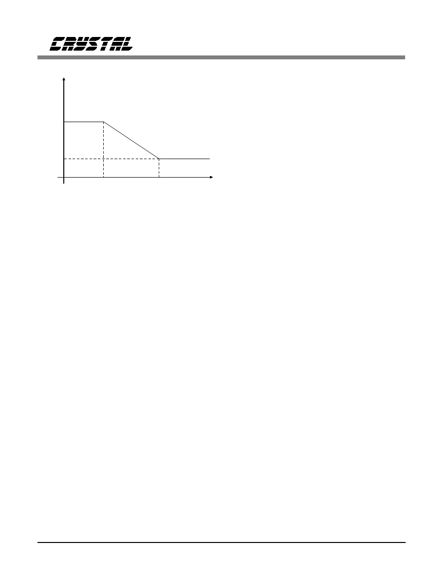
T2 = 15
m
s
T1=50
m
s
F1
F2
3.183 kHz
10.61 kHz
Figure 3. De-Emphasis Curve (Fs = 44.1kHz)
CS4330, CS4331, CS4333
DS136F1
9
Internal SCLK Mode
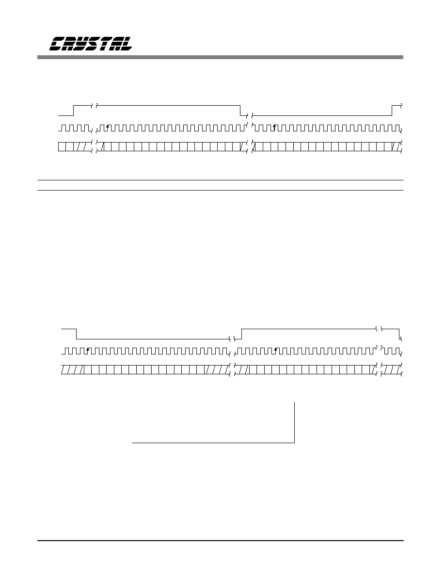
External SCLK Mode
Right Justified, 18-Bit Data
Data Valid on Rising Edge of SCLK
INT SCLK = 64 Fs if MCLK/LRCK = 256 or 512
INT SCLK = 48 Fs if MCLK/LRCK = 384
Right Justified, 18-Bit Data
Data Valid on Rising Edge of SCLK
SCLK must have at least 36 cycles per LRCK
Figure 4. CS4330 Data Format
LRCK
SCLK
Left Channel
Right Channel
SDATA
6
5
4
3
2
1
0
9
8
7
15 14 13 12 11 10
1
0
6
5
4
3
2
1
0
9
8
7
15 14 13 12 11 10
17 16
17 16
LRCK
SCLK
Left Channel
Right Channel
SDATA
6
5
4
3
2
1
0
9
8
7
15 14 13 12 11 10
6
5
4
3
2
1
0
9
8
7
15 14 13 12 11 10
Internal SCLK Mode
I
2
S, 16-Bit Data
Data Valid on Rising Edge of SCLK
INT SCLK = 32 Fs if MCLK/LRCK = 512 or 256
INT SCLK = 48 Fs if MCLK/LRCK = 384
Figure 5. CS4331 Internal SCLK Data Format (I
2
S)
CS4330, CS4331, CS4333
10
DS136F1
LRCK
SCLK
Left Channel
Right Channel
SDATA
6
5
4
3
2
1
0
9
8
7
15 14 13 12 11 10
6
5
4
3
2
1
0
9
8
7
15 14 13 12 11 10
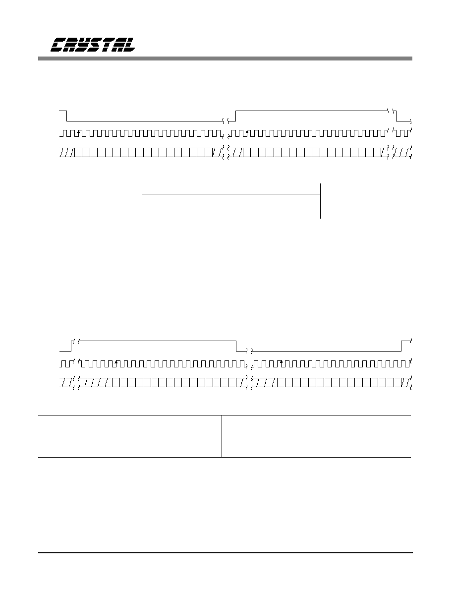
Internal SCLK Mode
External SCLK Mode
Right Justified, 16-Bit Data
Data Valid on Rising Edge of SCLK
INT SCLK = 32 Fs if MCLK/LRCK = 512 or 256
INT SCLK = 48 Fs if MCLK/LRCK = 384
Right Justified, 16-Bit Data
Data Valid on Rising Edge of SCLK
SCLK must have at least 32 cycles per LRCK
Figure 7. CS4333 SCLK Data Format
LRCK
SCLK
Left Channel
Right Channel
SDATA
6
5
4
3
2
1
0
9
8
7
15 14 13 12 11 10
17 16
6
5
4
3
2
1
0
9
8
7
15 14 13 12 11 10
17 16
External SCLK Mode
I
2
S, 18-Bit Data
Data Valid on Rising Edge of SCLK
SCLK must have at least 36 cycles per LRCK
Figure 6. CS4331 External SCLK Data Format (I
2
S)
CS4330, CS4331, CS4333
DS136F1
11
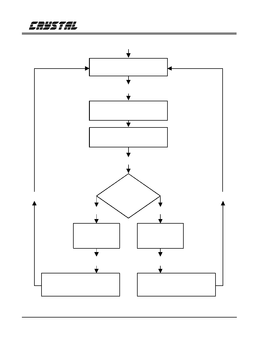
USER: Apply Power
Power-Down Mode
USER: Apply MCLK and LRCK
256/384/512
MCLK/LRCK Determination
USER: set SCLK mode
Power Supply Determination
+3 or +5 Volt mode
USER: Apply SDATA
SCLK mode
Normal Operation
De-emphasis
available
Normal Operation
De-emphasis
not available
USER: Apply SDATA
Analog Output
is Generated
Analog Output
is Generated
USER: Remove Clocks
USER: Remove Clocks
external
internal
Figure 8. CS4330/31/33 Initialization and Power-Down Sequence
CS4330, CS4331, CS4333
12
DS136F1

mended on the analog outputs. The required ca-
pacitor value is defined by:
C
=
1
(
2
)
(
Fs
)
(
2400
)
(
2
)
Example: Fs = 48 kHz
C = 690 pF
A value of 680 pF may be used with only 1.45%
error which is negligible.
Combined Digital and Analog Filter Response
The frequency response of the combined analog
switched-capacitor filter, digital filter, and off-
chip single pole RC-filter at 2 Fs, is shown in
Figures 9, 10, 11, and 12. The overall response
is clock dependent and will scale with Fs. Note
that the response plots have been normalized to
Fs and can be de-normalized by multiplying the
X-axis scale by Fs.
Figure 9. CS4330/31/33 Combined Digital and Analog
Filter Stopband Rejection
Figure 10. CS4330/31/33 Combined Digital and Analog
Filter Transition Band
Figure 11. CS4330/31/33 Combined Digital and Analog
Filter Transition Band
Figure 12. CS4330/31/33 Combined Digital and Analog
Filter Passband Ripple
CS4330, CS4331, CS4333
DS136F1
13
Performance Plots
The following CS4330/31/33 measurement plots
were taken on the CDB4330/31/33 evaluation
board with an Audio Precision Dual Domain
System One. All plots are done in +5V mode at
a 48 kHz sampling rate, and are shown in Fig-
ures 13-20.
Figure 13 shows the CS4330/31/33 frequency re-
sponse. The response is flat to 20 kHz
±
0.1dB
as specified.
Figure 14 shows THD+N versus signal ampli-
tude for a 1 kHz 20-bit dithered input signal.
Figure 15 shows a 16k FFT of a 1 kHz full-scale
input signal. The signal has been filtered by a
notch filter within the System One to remove the
fundamental component of the signal. This mini-
mizes the distortion created in the analyzer
analog-to-digital converter. This technique is dis-
c usse d by Au d io Pre cisio n in the 10t h
anniversary edition of AUDIO.TST.
Figure 16 shows a 16k FFT of a 1 kHz -3 dBFs
input signal. The signal has been filtered by a
notch filter within the System One to remove the
fundamental component of the signal.
Figure 17 shows a 16k FFT of a 1 kHz -20 dBFs
input signal. The signal has been filtered by a
notch filter within the System One to remove the
fundamental component of the signal.
Figure 18 shows a 16k FFT of a 1 kHz -60 dBFs
input signal.
Figure 19 shows a 16k FFT of a 1 kHz -90 dBFs
input signal.
Figure 20 shows the fade-to-noise linearity. The
input signal is a dithered 18-bit 500 Hz sine
Figure 13. Frequency Response
Figure 14. THD+N vs. Amplitude
Figure 15. 0 dBFs FFT
CS4330, CS4331, CS4333
14
DS136F1

wave which fades from -60 to -120 dBFs. Dur-
ing the fade, the output from the CS4330/31/33
is measured and compared to the ideal level. No-
tice the very close tracking of the output level to
the ideal, even at low level inputs. This indicates
very good low-level linearity, one of the key
benefits of delta-sigma digital-to-analog conver-
sion.
Figure 19. -90 dBFs FFT
Figure 20. Fade-to-Noise Linearity
Figure 18. -60 dBFs FFT
Figure 16. -3 dBFs FFT
Figure 17. -20 dBFs FFT
CS4330, CS4331, CS4333
DS136F1
15

Configuration Register
The CS4330, CS4331, CS4333 support multiple
2's-complement data/clock formats. The required
format is governed by the contents of the Con-
figuration Register. The 5-bit register determines
which serial data format is acceptable, the fre-
quency of the Internal Serial Clock, on which
edge of SCLK audio data must be valid, and the
number of bits to be loaded into the input buffer.
On initial power-up, the register is loaded with
the default settings, and it is not necessary to
write to the register if this format is appropriate.
The default settings are shown in Figures 4-7.
The 8-bit code includes a 3-bit preamble to pre-
vent accidental access to the Configuration
Register. Each bit of the code is read on the fall-
ing edge of LRCK as shown in the Figures 21
and 22. The code 01000000 is considered to be
an error condition and is ignored. The configura-
tion routine requires that the SDATA pin is held
high, as shown in Figures 21 and 22, to prevent
accidental writing to the register. The Configura-
tion Register is only accessible prior to entering
the External Serial Clock Mode. For I
2
S mode,
the user must set B6 to 0, and B7 to 1.
B1
B2
B3
B4
B5
B6
B7
B8
B1
B2
B3
Configuration Access Code
0
1
0
Access Allowed
All other Codes
Access Denied
B4
B5
Internal SCLK Mode only
Sets Internal SCLK/LRCK Ratio *
0
0
SCLK/LRCK = 32
0
1
Reserved
1
0
SCLK/LRCK = 64
1
1
SCLK/LRCK = 128
* The Internal SCLK will be 48 Fs, if the
MCLK/LRCK ratio is 384
◊.
B4
B5
External SCLK Mode only
Selects Data Sampling edge of SCLK
1
0
Rising edge of SCLK
1
1
Falling edge of SCLK
B6
Left or Right Justified Data
in relation to LRCK transition
0
Left Justified
1
Right Justified
B7
I
2
S Data Format
0
Disabled
1
Enabled
B8
Sets the number of Bits
0
18 Bits
1
16 Bits
Schematic & Layout Review Service
Confirm Optimum
Schematic & Layout
Before Building Your Board.
Confirm Optimum
Schematic & Layout
Before Building Your Board.
For Our Free Review Service
Call Applications Engineering.
For Our Free Review Service
Call Applications Engineering.
C a l l : ( 5 1 2 ) 4 4 5 - 7 2 2 2
CS4330, CS4331, CS4333
16
DS136F1
Figure 22. Configuration Timing
Figure 21. Configuration Operation
Parameter
Symbol
Min
Typ
Max
Units
DEM/SCLK TIMING
DEM/SCLK valid to LRCK falling setup time
t
clrs
20
-
-
ns
LRCK falling to DEM/SCLK hold time
t
clrh
20
-
-
ns
SDATA setup time
t
setup
1
-
-
us
SDATA hold time
t
hold
1
-
-
us
Table 2. Configuration Timing Characteristics
CS4330, CS4331, CS4333
DS136F1
17

REFERENCES
1)"An 18-Bit, 8-Pin Stereo Digital-to-Analog
Converter" by J.J. Paulos, A.W. Krone, G.D
Kamath, and S.T. Dupuie. Paper presented at the
97th Convention of the Audio Engineering Soci-
ety, November 1994.
2)"How to Achieve Optimum Performance from
Delta-Sigma A/D & D/A Converters" by Steven
Harris. Paper presented at the 93rd Convention
of the Audio Engineering Society, October 1992.
3)"Multiplier-Free Interpolation for Oversampled
Digital-to-Analog Conversion" by Jeffrey W.
Scott. Paper presented at the 92nd Convention of
the Audio Engineering Society, March 1992.
4)"An 18-Bit Stereo D/A Converter With Inte-
grated Digital and Analog Filters" by Nav S.
Sooch, Jeffrey W. Scott. Paper presented at the
91st Convention of the Audio Engineering Soci-
ety, November 1991.
5)CDB4330/31/33 Evaluation board Data Sheet;
DS136DB2 MAR'96
CS4330, CS4331, CS4333
18
DS136F1
PIN DESCRIPTIONS
Power Supply Connections
VA+ - Positive Analog Power, PIN 7.
Positive analog supply. Nominally +5V or +3V.
AGND - Analog Ground, PIN 6.
Analog ground reference.
Analog Outputs
AOUTL - Analog Left Channel Output, PIN 8.
Analog output for the left channel. Typically 3.7 Vpp for a full-scale input signal at VA+ = 5V
and 1.85 Vpp at VA+ = 3V.
AOUTR - Analog Right Channel Output, PIN 5.
Analog output for the right channel. Typically 3.7 Vpp for a full-scale input signal at VA+ = 5V
and 1.85 Vpp at VA+ = 3V.
Digital Inputs
MCLK - Master Clock Input, PIN 4.
The frequency must be 256
◊
, 384
◊
, or 512
◊
the input sample rate (Fs).
LRCK - Left/Right Clock, PIN 3.
This input determines which channel is currently being input on the Audio Serial Data Input
pin, SDATA.
SDATA - Audio Serial Data Input, PIN 1.
Two's complement MSB-first serial data is input on this pin. The data is clocked into the
CS4330, CS4331, and CS4333 via internal or external SCLK and the channel is determined by
LRCK.
DEM/SCLK - De-emphasis / External serial clock input , PIN 2.
A dual-purpose input used for de-emphasis filter control or external serial clock input.
SERIAL DATA INPUT
SDATA
AOUTL
ANALOG LEFT CHANNEL OUTPUT
DE-EMPHASIS / SCLK
DEM/SCLK
VA+
ANALOG POWER
LEFT / RIGHT CLOCK
LRCK
AGND
ANALOG GROUND
MASTER CLOCK
MCLK
AOUTR
ANALOG RIGHT CHANNEL OUTPUT
7
2
6
3
5
4
8
1
CS4330, CS4331, CS4333
DS136F1
19

PARAMETER DEFINITIONS
Total Harmonic Distortion + Noise (THD+N)- The ratio of the rms value of the signal to the rms
sum of all other spectral components over the specified bandwidth (typically 10 Hz to 20 kHz),
including distortion components. Expressed in decibels.
Dynamic Range - The ratio of the full scale rms value of the signal to the rms sum of all other
spectral components over the specified bandwidth. Dynamic range is a signal-to-noise
measurement over the specified bandwidth made with a -60 dBFs signal. 60 dB is then added to
the resulting measurement to refer the measurement to full scale. This technique ensures that
the distortion components are below the noise level and do not effect the measurement. This
measurement technique has been accepted by the Audio Engineering Society, AES17-1991, and
the Electronic Industries Association of Japan, EIAJ CP-307.
Interchannel Isolation - A measure of crosstalk between the left and right channels. Measured for
each channel at the converter's output with all zeros to the input under test and a full-scale
signal applied to the other channel. Units in decibels.
Interchannel Gain Mismatch - The gain difference between left and right channels. Units in decibels.
Gain Error - The deviation from the nominal full scale analog output for a full scale digital input.
Gain Drift - The change in gain value with temperature. Units in ppm/
∞
C.
CS4330, CS4331, CS4333
20
DS136F1

ORDERING INFORMATION:
Model
Temperature
Package
CS4330-KS
-10 to +70∞C
8-pin Plastic SOIC
CS4331-KS
-10 to +70∞C
8-pin Plastic SOIC
CS4333-KS
-10 to +70∞C
8-pin Plastic SOIC
CS4330-BS
-40 to +85∞C
8-pin Plastic SOIC
CS4331-BS
-40 to +85∞C
8-pin Plastic SOIC
CS4333-BS
-40 to +85∞C
8-pin Plastic SOIC
F
G
J
I
H
B
A
MILLIMETERS
INCHES
MIN
MAX
MAX
MIN
DIM
H
I
J
A
B
TYP
1.27
0.050
TYP
D
0
0.010
0
0.25
E
0.070
0.074
1.77
1.88
0.006
0.010
0.15
0.25
8
0
8
0
0.030
0.019
0.48
0.76
0.319
0.302
0.203
0.210
5.15
5.35
7.67
8.1
5.18
5.4
0.204
0.213
D
C
8-Pin
SOIC
E
F
0.33
0.51
0.020
G
C
0.013
PACKAGE DIMENSIONS
Note: The EIAJ package is not a standard JEDEC package size
CS4330, CS4331, CS4333
DS136F1
21

∑ Notes ∑

Features
∑
Demonstrates recommended layout
and grounding arrangements
∑
CS8412 Receives AES/EBU, S/PDIF,
& EIAJ-340 Compatible Digital Audio
∑
Digital and Analog Patch Areas
∑
Requires only a digital signal source
and power supplies for a complete
Digital-to-Analog-Converter system
General Description
The CDB4330/31/33 evaluation board is an excellent
means for quickly evaluating the CS4330/31/33 18-bit,
stereo D/A converter. Evaluation requires an analog
signal analyzer, a digital signal source and a power
supply. Analog outputs are provided via RCA connec-
tors for both channels.
The CS8412 digital audio receiver I.C. provides the
system timing necessary to operate the CS4330/31/33
and will accept AES/EBU, S/PDIF, and EIAJ-340
compatible audio data. The evaluation board may also
be configured to accept external timing signals for op-
eration in a user application during system
development.
ORDERING INFORMATION:
CDB4330, CDB4331,
CDB4333
Evaluation Board for CS4330 / CS4331 / CS4333
CDB4330
CDB4331 CDB4333
Digital
Audio
Input
I/O for
Clocks
and Data
CS8412
Digital
Audio
Interface
CS4330/31/33
Analog
Filter
Crystal Semiconductor Corporation
P.O. Box 17847, Austin, TX 78760
(512) 445-7222 Fax: (512) 445 7581
MAR '96
DS136DB2
23
Copyright
©
Crystal Semiconductor Corporation 1996
(All Rights Reserved)

CDB4330/31/33 System Overview
The CDB4330/31/33 evaluation board is an ex-
c el l en t mean s of qu ick ly eval uat ing th e
CS4330/31/33. The CS8412 digital audio inter-
face receiver provides an easy interface to digital
audio signal sources including the majority of
digital audio test equipment. The evaluation
board also allows the user to supply clocks and
data through a 10-pin header for system develop-
ment.
The CDB4330/31/33 schematic has been parti-
tioned into 5 schematics shown in Figures 2
through 7. Each partitioned schematic is repre-
sented in the system diagram shown in Figure 1.
Notice that the the system diagram also includes
the interconnections between the partitioned
schematics.
CS4330/31/33 Digital to Analog Converter
A description of the CS4330/31/33 is included in
the CS4330/31/33 data sheet.
CS8412 Digital Audio Receiver
The system receives and decodes the standard
S/PDIF data format using a CS8412 Digital
Audio Receiver, Figure 4. The outputs of the
CS8412 include a serial bit clock, serial data,
left-right clock (FSYNC), de-emphasis control
and a 256Fs master clock. The operation of the
CS8412 and a discussion of the digital audio in-
t erface a re inc lud ed in t he 19 94 Crystal
Semiconductor Audio Data Book.
During normal operation, the CS8412 operates in
the Channel Status mode where the LED's dis-
play channel status information for the channel
selected by the CSLR/FCK jumper. This allows
the CS8412 to decode and supply the de-empha-
sis bit from the digital audio interface for control
of the CS4330/31/33 de-emphasis filter via
pin 3, CC/F0, of the CS8412.
When the Error Information Switch is activated,
the CS8412 operates in the Error and Frequency
information mode. The information displayed by
the LED's can be decoded by consulting the
CS8412 data sheet. If the Error Information
Switch is activated, and the CS4330/31/33 is in
the internal serial clock mode, then it is likely
t h at t h e de -e mp ha si s c on t rol for t he
CS4330/31/33 will be erroneous and produce an
incorrect audio output.
Encoded sample frequency information can be
displayed provided a proper clock is being ap-
plied to the FCK pin of the CS8412. When an
LED is lit, this indicates a "1" on the corre-
sponding pin located on the CS8412. When an
LED is off, this indicates a "0" on the corre-
sponding pin. Neither the L or R option of
CSLR/FCK should be selected if the FCK pin is
being driven by a clock signal.
The evaluation board has been designed such
that the input can be either optical or coax, Fig-
ure 6. It is not necessary to select the active
input. However, both inputs can not be driven si-
multaneously.
CS8412 Data Format
The CS8412 data format can be set with jumpers
M0, M1, M2, and M3. These formats are shown
in the CS8412 datasheet found in the 1994 Crys-
tal Semiconductor Audio Data Book. The format
selected must be compatible with the corre-
sponding data format of the CS4330/31/33
shown in Figures 4-7 of the CS4330/31/33
datasheet. The default settings for M0-M3 on the
evaluation board are given in Tables 2-4. The
compatible data formats we have chosen for the
CS8412 and CS4330/31/33 are:
CS8412 format 6;CS4330
CS8412 format 2;CS4331 (External SCLK only)
CS8412 format 5;CS4333 (External SCLK only)
CDB4330, CDB4331, CDB4333
24
DS136DB2

Analog output filter
The recommended single pole filter required for
the CS4330/31/33 has been combined with a
unity gain output buffer (see Figure 2). The ana-
log output filter uses a Motorola MC33202
single supply, dual op-amp. The low pass filter
corner frequency is located at 2 Fs, or 88.2 kHz
and is calculated by:
F
=
1
(
2
)
(
R
8
||
R
9
)
(
C
29
)
F
=
1
(
2
)
(
15k
|| 6.65
k
)
(
390
pF
)
= 88.5 kHz
Power Supply Circuitry
Power is supplied to the evaluation board by
three binding posts (GND, +5V, +3V/+5V), See
Figure 7. The +5V input supplies power to the
+5 Volt digital circuitry (VD+5), while the
+3V/+5V input supplies power to the Voltage
Level Converter (VD+3/+5), and CS4330/31/33
(VA+3/+5) for evaluation in either +3 or +5 Volt
mode. The op-amp is supplied from the analog
supply (VA+) which can be derived from either
the +5V post (VA+5) or the +3/+5V post
(VA+3/+5) depending upon which Ferrite bead
(L4 or L5) is installed. The evaluation board is
configured with VA+ derived from VA+5 (L5 in-
stalled). To derive VA+ from the +3V/+5V post
(VA+3/+5), remove the Ferrite bead at L5, and
install it at L4.
Input/Output for Clocks and Data
The evaluation board has been designed to allow
the interface to external systems via the 10-pin
header, J1. This header allows the evaluation
board to accept externally generated clocks and
data. The schematic for the clock/data I/O is
shown in Figure 5. The 74HC243 transceiver
functions as an I/O buffer where the CLK
SOURCE jumper determines if the transceiver
operates as a transmitter or receiver.
The transceiver operates as a transmitter with the
CLK SOURCE jumper in the 8412 position.
LRCK, SDATA, and SCLK from the CS8412
will be available on J1. J22 must be in the 0 po-
sition and J23 must be in the 1 position for
MCLK to be an output and to avoid bus conten-
tion on MCLK.
The transceiver operates as a receiver with the
CLK SOURCE jumper in the EXTERNAL posi-
tion. LRCK, SDATA and SCLK on J1 become
inputs. The CS8412 must be removed from the
evaluation board for operation in this mode.
There are 2 options for the source of MCLK in
the External Clock Source mode. MCLK can be
an input with J23 in the 1 position and J22 in the
0 position. However, the recommended mode of
operation is to generate MCLK on the evaluation
board. MCLK becomes an output with LRCK,
SCLK and SDATA inputs. This technique insures
that the CS4330/31/33 receives a jitter free clock
to maximize performance. This can be accom-
plished by installing a crystal oscillator into U5,
see Figure 4 (the socket for U5 is located within
the footprint for the CS8412) and placing J22 in
the 1 position and J23 in the 0 position.
Grounding and Power Supply Decoupling
The CS4330/31/33 requires careful attention to
power supply and grounding arrangements to op-
t i miz e p er fo rman ce. Fi gure 2 sh ows t he
re commend ed power a rrangements. The
CS4330/31/33 is positioned over the analog
ground plane near the digital/analog ground
plane split. These ground planes are connected
elsewhere on the board. This layout technique is
used to minimizing digital noise and to insure
proper power supply matching/sequencing. The
decoupling capacitors are located as close to the
CS4330/31/33 as possible. Extensive use of
ground plane fill on both the analog and digital
sections of the evaluation board yield large re-
ductions in radiated noise effects.
CDB4330, CDB4331, CDB4333
DS136DB2
25

JUMPER
PURPOSE
POSITION
FUNCTION SELECTED
CSLR/FCK
selects channel for
CS8412 channel status
information
L
See CS8412 data sheet for details
R
Clock
Select
Selects source of
system clocks and data
*8412
CS8412 clock/data source
EXT
External clock/data source
J22
J23
Selects MCLK as Input
or Output
*0
*1
See
Input/Output for Clocks and
Data section of text
M0
CS8412 mode select
*Low
See CS8412 data sheet
for details
M1
*High
M2
*High
M3
*Low
SCLK
Selects SCLK Mode
INT
Internal SCLK Mode
*EXT
External SCLK Mode
DEM_8412
Selects source of de-
emphasis control
*Low
CS8412 de-emphasis
High
De-emphasis input static high
* Default setting from factory
Table 2. CDB4330 Jumper Selectable Options
CONNECTOR
INPUT/OUTPUT
SIGNAL PRESENT
+5V
input
(VD+5V) for CS8412 and digital section
input
(VA+) for Analog output filter op-amp
(configured for +5V)
+3/+5V
input
(VD+3/+5V) for Voltage Level Converter
input
(VA+3/+5V) for CS4330/31/33
GND
input
ground connection from power supply
Digital Input
input
digital audio interface input via coax
Optical Input
input
digital audio interface input via optical
MCLK, SCLK,
LRCK
input/output
I/O for master, serial, and left/right clocks
SDATA
input/output
I/O for serial data
AOUTL
output
left channel analog output
AOUTR
output
right channel analog output
Table 1. System Connections
CDB4330, CDB4331, CDB4333
26
DS136DB2

JUMPER
PURPOSE
POSITION
FUNCTION SELECTED
CSLR/FCK
selects channel for
CS8412 channel status
information
L
See CS8412 data sheet for details
R
Clock
Select
Selects source of
system clocks and data
*8412
CS8412 clock/data source
EXT
External clock/data source
J22
J23
Selects MCLK as Input
or Output
*0
*1
See
Input/Output for Clocks and
Data section of text
M0
CS8412 mode select
*Low
See CS8412 data sheet
for details
M1
*High
M2
*Low
M3
*Low
SCLK
Selects SCLK Mode
INT
Internal SCLK Mode (Note 1)
*EXT
External SCLK Mode (Note 1)
DEM_8412
Selects source of de-
emphasis control
*Low
CS8412 de-emphasis
High
De-emphasis input static high
* Default setting from factory
Note 1. The CS8412 output data format requires the CS4331 be in the External SCLK Mode
Table 3. CDB4331 Jumper Selectable Options
JUMPER
PURPOSE
POSITION
FUNCTION SELECTED
CSLR/FCK
selects channel for
CS8412 channel status
information
L
See CS8412 data sheet for details
R
Clock
Select
Selects source of
system clocks and data
*8412
CS8412 clock/data source
EXT
External clock/data source
J22
J23
Selects MCLK as Input
or Output
*0
*1
See
Input/Output for Clocks and
Data section of text
M0
CS8412 mode select
*High
See CS8412 data sheet
for details
M1
*Low
M2
*High
M3
*Low
SCLK
Selects SCLK Mode
INT
Internal SCLK Mode (Note 1)
*EXT
External SCLK Mode (Note 1)
DEM_8412
Selects source of de-
emphasis control
*Low
CS8412 de-emphasis
High
De-emphasis input static high
* Default setting from factory
Note 1. The CS8412 output data format requires the CS4333 be in the External SCLK Mode
Table 4. CDB4333 Jumper Selectable Options
CDB4330, CDB4331, CDB4333
DS136DB2
27

Digital
Audio
Input
Fig 6
I/O for
Clocks
and Data
Fig 5
CS8412
Digital
Audio
Interface
RX
N
RX
P
MCLK
LRCK
SCLK
SDATA
Fig 2
AOUTL
AOUTR
Fig 2
Fig 4
CS4330/31/33
Power
Down
Fig 3
Voltage
Level
Converter
Fig 3
MCLK
LRCK
SCLK
SDATA
Analog
Filter
Figure 1. System Block Diagram and Signal Flow
CDB4330, CDB4331, CDB4333
28
DS136DB2
Figure 2. CS4330/31/33 and Connections
CDB4330, CDB4331, CDB4333
DS1
3
6
DB2
29

Figure 3. Voltage Level Conversion and Power Down Circuitry
CDB4330, CDB4331, CDB4333
30
DS136DB2

NOTE: U2 and U5 cannot be installed simultaneously
Figure 4. CS8412 Digital Audio Receiver Connections
CDB4330, CDB4331, CDB4333
DS1
3
6
DB2
31
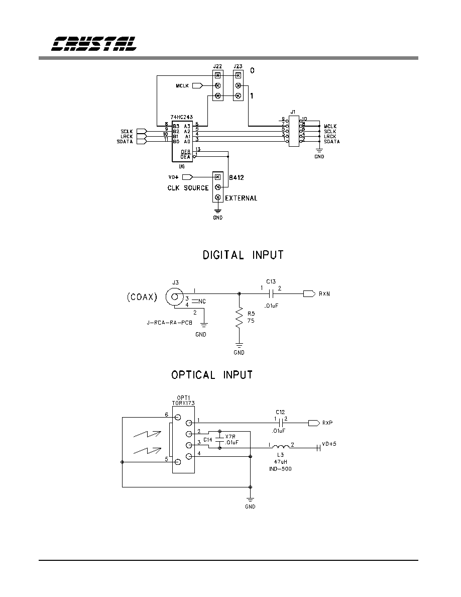
Figure 5. I/O Interface for Clocks and Data
Optical Toshiba part TORX173 available through Insight Electronics
Figure 6. Digital Audio Input
CDB4330, CDB4331, CDB4333
32
DS136DB2
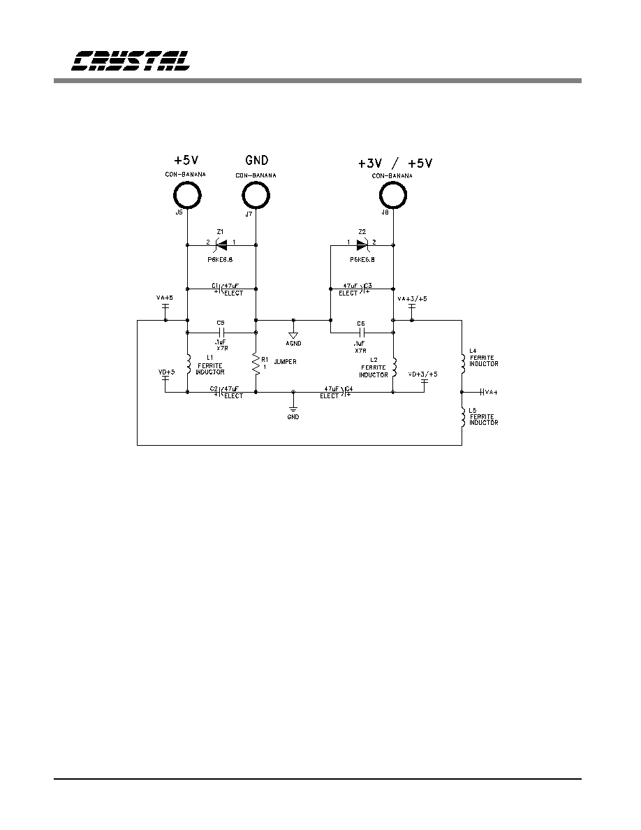
Figure 7. Power Supply
CDB4330, CDB4331, CDB4333
DS136DB2
33

Figure 8. CDB4330/31/33 Component Side Silkscreen
CDB4330, CDB4331, CDB4333
34
DS136DB2

Figure 9. CDB4330/31/33 Component Side (top)
CDB4330, CDB4331, CDB4333
DS136DB2
35

Figure 10. CDB4330/31/33 Solder Side (bottom)
CDB4330, CDB4331, CDB4333
36
DS136DB2

∑ Notes ∑

Advance product information describes products which are in development and subject to development changes. Cirrus Logic, Inc. has made
best efforts to ensure that the information contained in this document is accurate and reliable. However, the information is subject to change
without notice and is provided "AS IS" without warranty of any kind (express or implied). No responsibility is assumed by Cirrus Logic, Inc. for
the use of this information, nor for infringements of patents or other rights of third parties. This document is the property of Cirrus Logic, Inc. and
implies no license under patents, copyrights, trademarks, or trade secrets. No part of this publication may be copied, reproduced, stored in a
retrieval system, or transmitted, in any form or by any means (electronic, mechanical, photographic, or otherwise). Furthermore, no part of this
publication may be used as a basis for manufacture or sale of any items without the prior written consent of Cirrus Logic, Inc. The names of
products of Cirrus Logic, Inc. or other vendors and suppliers appearing in this document may be trademarks or service marks of their respective
owners which may be registered in some jurisdictions. A list of Cirrus Logic, Inc. trademarks and service marks can be found at http://www.cir-
rus.com.