
Preliminary Product Information
This document contains information for a new product.
Cirrus Logic reserves the right to modify this product without notice.
1
Copyright
Cirrus Logic, Inc. 2002
(All Rights Reserved)
Cirrus Logic, Inc.
P.O. Box 17847, Austin, Texas 78760
http://www.cirrus.com
CS4341A
24-Bit, 192 kHz Stereo DAC with Volume Control
Features
101 dB Dynamic Range
-91 dB THD+N
+3.3 V or +5 V Power Supply
50 mW with 3. 3V supply
Low Clock Jitter Sensitivity
Filtered Line Level Outputs
On-Chip Digital De-emphasis for 32, 44.1,
and 48 kHz
ATAPI Mixing
Digital Volume Control with Soft Ramp
≠ 94 dB Attenuation
≠ 1 dB Step Size
≠ Zero Crossing Click-Free Transitions
Up to 200 kHz Sample Rates
Automatic Mode Detection for Sample Rates
between 4 and 2 0 0kHz
Pin Compatible with the CS4341
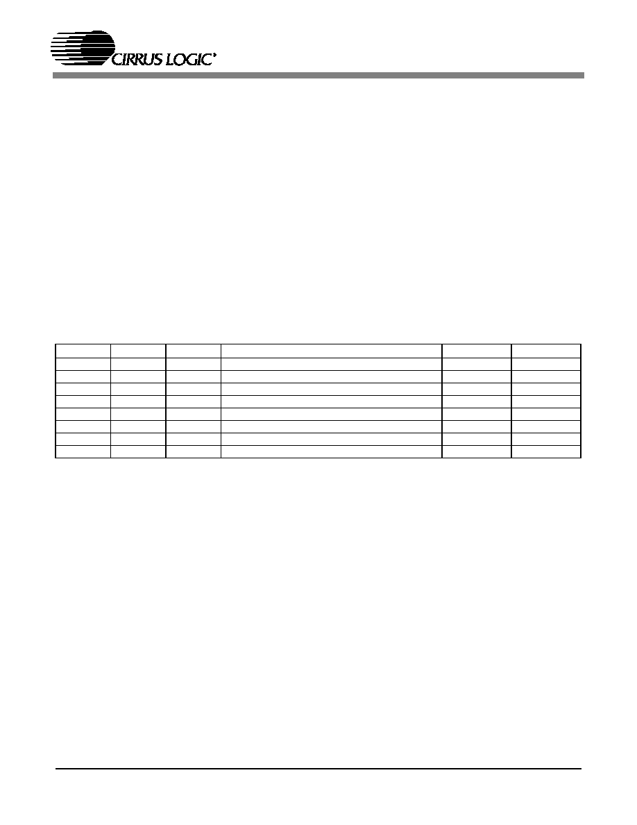
Description
The CS4341A is a complete stereo digital-to-analog sys-
tem including digital interpolation, fourth-order delta-
sigma digital-to-analog conversion, digital de-emphasis,
volume control, channel mixing and analog filtering. The
advantages of this architecture include: ideal differential
linearity, no distortion mechanisms due to resistor
matching errors, no linearity drift over time and tempera-
ture and a high tolerance to clock jitter.
The CS4341A accepts data at all standard audio sample
rates up to 192 kHz, consumes very little power, oper-
ates over a wide power supply range and is pin
compatible with the CS4341, as described in section 3.1.
These features are ideal for DVD audio players.
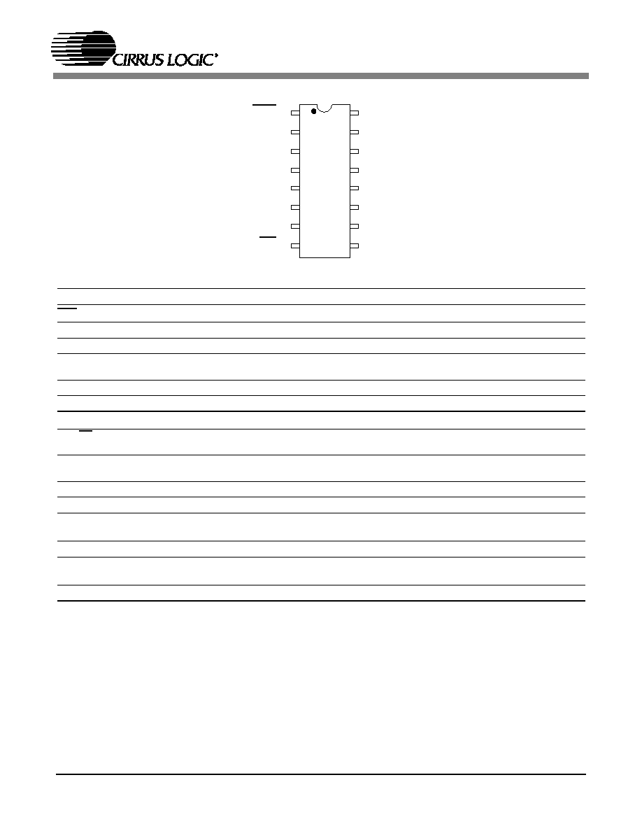
ORDERING INFORMATION
CS4341A-KS
16-pin SOIC, -10 to 70 ∞C
CDB4341A
Evaluation Board
V olum e Control
Interpolation Filter
DA C
A nalog Filter
C ontrol Port
Interface
V olum e Control
Interpolation Filter
A nalog Filter
Ser
i
al
Aud
i
o
In
te
r
f
a
c
e
SC L/C C LK
M U T EC
AD 0/C S
AO U T A
AO UT B
RST
LRC K
SD IN
M C LK
SD A/CD IN
DA C
E xternal
Mute C ontrol
S CLK
Mixer
˜2
AUG `02
DS582PP1

CS4341A
2
DS582PP1
TABLE OF CONTENTS
1. PIN DESCRIPTION ................................................................................................................... 5
2. TYPICAL CONNECTION DIAGRAM ...................................................................................... 6
3. APPLICATIONS ........................................................................................................................ 7
3.1 Upgrading from the CS4341 to the CS4341A .................................................................... 7
3.2 Sample Rate Range/Operational Mode Detect .................................................................. 7
3.2.1 Auto-Detect Enabled ............................................................................................. 7
3.2.2 Auto-Detect Disabled ............................................................................................ 7
3.3 System Clocking ................................................................................................................ 8
3.4 Digital Interface Format ...................................................................................................... 8
3.5 De-Emphasis Control ......................................................................................................... 9
3.6 Recommended Power-up Sequence ................................................................................. 9
3.7 Popguard
Æ
Transient Control ........................................................................................... 10
3.7.1 Power-up ............................................................................................................. 10
3.7.2 Power-down ........................................................................................................ 10
3.7.3 Discharge Time ................................................................................................... 10
3.8 Grounding and Power Supply Arrangements .................................................................. 10
3.9 Control Port Interface ....................................................................................................... 11
3.9.1 MAP Auto Increment ........................................................................................... 11
3.9.2 I2C Mode ............................................................................................................. 11
3.9.2a I2C Write .............................................................................................. 11
3.9.2b I2C Read .............................................................................................. 12
3.9.3 SPI Mode ............................................................................................................ 13
3.9.3a SPI Write .............................................................................................. 13
3.10 Memory Address Pointer (MAP) .............................................................................. 14
3.10.1 INCR (Auto Map Increment Enable) ............................................................................ 14
3.10.2 MAP (Memory Address Pointer) .................................................................................. 14
4. REGISTER QUICK REFERENCE .......................................................................................... 14
Contacting Cirrus Logic Support
F or a co m p le te listing of D ire ct Sa les, D is trib utor, an d S a le s R ep res en ta tiv e co nta cts, visit the C irru s Lo gic w e b site at:
http://w ww.cirrus.com /corporate/contacts/sales.cfm
IMPORTANT NOTICE
"Preliminary" product information describes products that are in production, but for which full characterization data is not yet available. "Advance" product infor-
mation describes products that are in development and subject to development changes. Cirrus Logic, Inc. and its subsidiaries (" Cirrus") believe that the infor-
mation contained in this docum ent is accurate and reliable. However, the inform ation is subject to change without notice and is provided "AS IS" without warranty
of any kind (express or implied). Customers are advised to obtain the latest version of relevant information to verify, before placing orders, that information being
relied on is current and complete. All products are sold subject to the terms and conditions of sale supplied at the time of order acknowledgment, including those
pertaining to warranty, patent infringem ent, and limitation of liability. No responsibility is assumed by Cirrus for the use of this information, including use of this
information as the basis for manufacture or sale of any items, or for infringement of patents or other rights of third parties. This document is the property of Cirrus
and by furnishing this information, Cirrus grants no license, express or im plied under any patents, mask work rights, copyrights , trademarks, trade secrets or
other intellectual property rights. Cirrus owns the copyrights of the information contained herein and gives consent for copies to be made of the information only
for use within your organization with respect to Cirrus integrated circuits or other parts of Cirrus. This consent does not extend to other copying such as copying
for general distribution, advertising or promotional purposes, or for creating any work for resale.
An export per mit needs to be obtained from the competent authorities of the Japanese Government if any of the products or technologies described in this ma-
terial and controlled under the "Foreign Exchange and Foreign Trade Law" is to be exported or taken out of Japan. An export license and/or quota needs to be
obtained from the competent authorities of the Chinese Government if any of the products or technologies described in this material is subject to the PRC Foreign
Trade Law and is to be exported or taken out of the PRC.
CERTAIN APPLICATIONS USING SEMICONDUCTOR PRODUCTS M AY INVOLVE POTENTIAL RISKS OF DEATH, PERSONAL INJURY, OR SEVERE
PROPERTY OR ENVIRONMENTAL DAM AGE ("CRITICAL APPLICATIONS"). CIRRUS PRODUCTS ARE NOT DESIGNED, AUTHORIZED, OR WARRANT-
ED TO BE SUITABLE FOR USE IN LIFE-SUPPORT DEVICES OR SYSTEMS OR OTHER CRITICAL APPLICATIONS. INCLUSION OF CIRRUS PRODUCTS
IN SUCH APPLICATIONS IS UNDERSTOOD TO BE FULLY AT THE CUSTOMER'S RISK.
Purchase of I
2
C com ponents of Cirrus Logic, Inc., or one of its sublicensed Associated Companies conveys a license under the Phillips I
2
C Patent Rights to use
those com ponents in a standard I
2
C system.
Cirrus Logic, Cirrus, and the Cirrus Logic logo designs are tradem arks of Cirrus Logic, Inc. All other brand and product names in this document may be trade-
marks or service marks of their respective owners.

CS4341A
DS582PP1
3
5. REGISTER DESCRIPTION .................................................................................................... 15
5.1 Mode Control 1 (address 00h) .......................................................................................... 15
5.2 Mode Control 2 (address 01h) .......................................................................................... 15
5.3 Transition and Mixing Control (address 02h).................................................................... 17
5.4 Channel A Volume Control (address 03h) ........................................................................ 20
5.5 Channel B Volume Control (address 04h) ........................................................................ 20
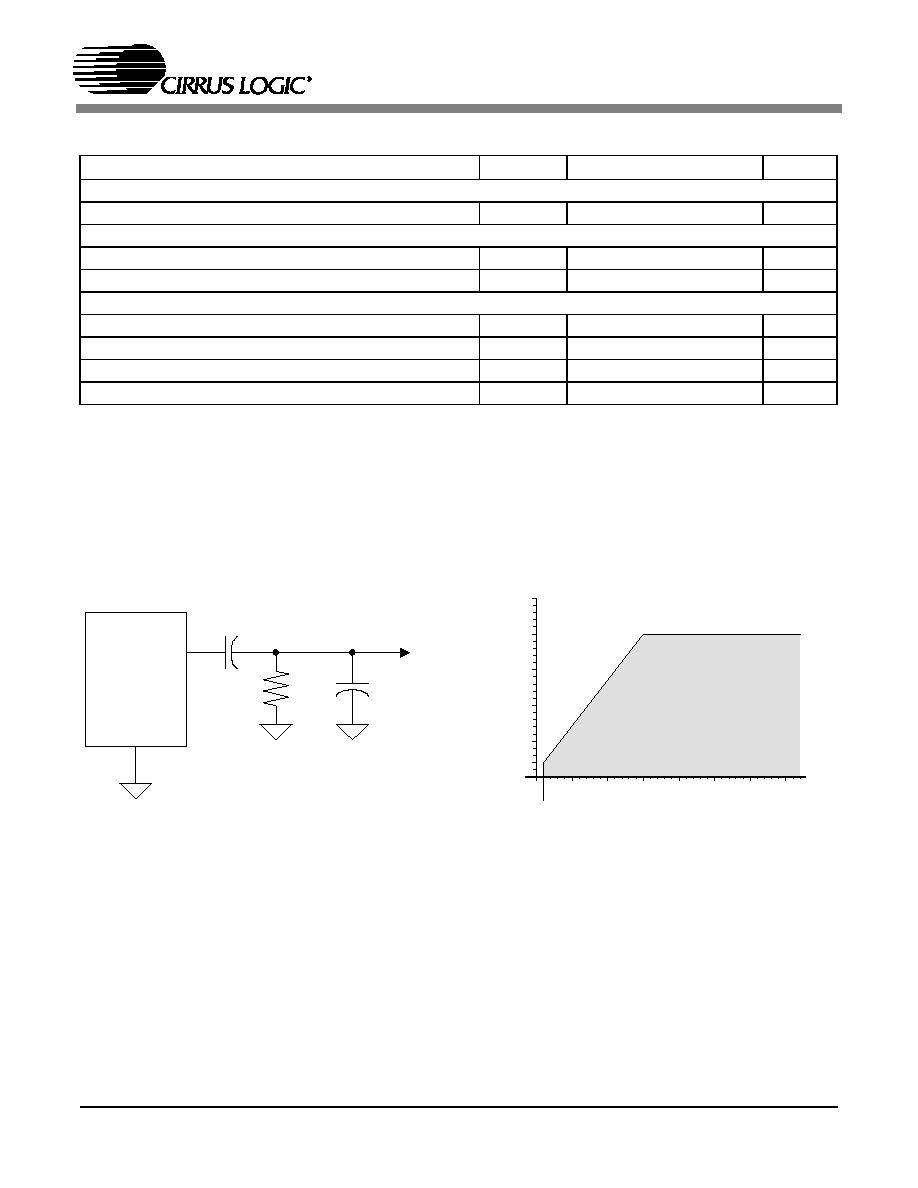
6. CHARACTERISTICS AND SPECIFICATIONS ...................................................................... 21
ANALOG CHARACTERISTICS (CS4341A-KS) ..................................................................... 21
COMBINED INTERPOLATION & ON-CHIP ANALOG FILTER RESPONSE ........................ 23
SWITCHING SPECIFICATIONS - SERIAL AUDIO INTERFACE .......................................... 26
SWITCHING SPECIFICATIONS - CONTROL PORT INTERFACE ....................................... 27
SWITCHING SPECIFICATIONS - CONTROL PORT INTERFACE ....................................... 28
DC ELECTRICAL CHARACTERISTICS ................................................................................ 29
DIGITAL INPUT CHARACTERISTICS ................................................................................... 29
DIGITAL INTERFACE SPECIFICATIONS ............................................................................. 29
THERMAL CHARACTERISTICS AND SPECIFICATIONS .................................................... 29
RECOMMENDED OPERATING SPECIFICATION .............................................................. 30
ABSOLUTE MAXIMUM RATINGS ......................................................................................... 30
7. PARAMETER DEFINITIONS .................................................................................................. 31
Total Harmonic Distortion + Noise (THD+N) .......................................................................... 31
Dynamic Range ...................................................................................................................... 31
Interchannel Isolation ............................................................................................................. 31
Interchannel Gain Mismatch ................................................................................................... 31
Gain Error ............................................................................................................................... 31
Gain Drift ................................................................................................................................ 31
8. REFERENCES ........................................................................................................................ 31
9. PACKAGE DIMENSIONS ...................................................................................................... 32
LIST OF FIGURES
Figure 1.
Typical Connection Diagram .......................................................................................... 6
Figure 2.
I
2
S Data ......................................................................................................................... 8
Figure 3.
Left Justified up to 24-Bit Data ....................................................................................... 9
Figure 4.
Right Justified Data ........................................................................................................ 9
Figure 5.
De-Emphasis Curve ....................................................................................................... 9
Figure 6.
Control Port Timing, I2C Mode .................................................................................... 12
Figure 7.
Control Port Timing, SPI mode .................................................................................... 13
Figure 8.
ATAPI Block Diagram .................................................................................................. 19
Figure 9.
Output Test Load ......................................................................................................... 22
Figure 10. Maximum Loading ........................................................................................................ 22
Figure 11. Single-Speed Stopband Rejection ............................................................................... 24
Figure 12. Single-Speed Transition Band ..................................................................................... 24
Figure 13. Single-Speed Transition Band (Detail) ......................................................................... 24
Figure 14. Single-Speed Passband Ripple ................................................................................... 24
Figure 15. Double-Speed Stopband Rejection .............................................................................. 24
Figure 16. Double-Speed Transition Band .................................................................................... 24
Figure 17. Double-Speed Transition Band (Detail) ....................................................................... 25
Figure 18. Double-Speed Passband Ripple .................................................................................. 25
Figure 19. Serial Input Timing ....................................................................................................... 26
Figure 20. Control Port Timing - I2C Mode ................................................................................... 27
Figure 21. Control Port Timing - SPI Mode ................................................................................... 28

CS4341A
4
DS582PP1
LIST OF TABLES
Table 1. CS4341A Auto-Detect .......................................................................................................... 7
Table 2. CS4341A Mode Select ......................................................................................................... 7
Table 3. Single-Speed Mode Standard Frequencies.......................................................................... 8
Table 4. Double-Speed Mode Standard Frequencies........................................................................ 8
Table 5. Quad-Speed Mode Standard Frequencies........................................................................... 8
Table 7. ATAPI Decode .................................................................................................................... 18
Table 8. Example Digital Volume Settings ....................................................................................... 20
CS4341A
DS582PP1
5
1.
PIN DESCRIPTION
1 5
2
1 4
3
1 3
4
1 6
1
1 1
6
1 0
7
9
8
1 2
5
RST
MUTEC
SDIN
AOUTA
SCLK
VA
LRCK
AGND
MCLK
AOUTB
SCL/CCLK
REF_GND
SDA/CDIN
VQ
AD0/CS
FILT+
Pin Name
#
Pin Description
RST
1
Reset (Input) - Powers down device when enabled.
SDIN
2
Serial Audio Data (Input) - Input for two's complement serial audio data.
SCLK
3
Serial Clock (Input) -Serial clock for the serial audio interface.
LRCK
4
Left Right Clock (Input) - Determines which channel, Left or Right, is currently active on the
serial audio data line.
MCLK
5
Master Clock (Input) - Clock source for the delta-sigma modulator and digital filters.
SCL/CCLK
6
Serial Control Port Clock (Input) - Serial clock for the control port interface.
SDA/CDIN
7
Serial Control Data I/O
(Input/Output)
- Input/Output for I
2
C data. Input for SPI data.
AD0/CS
8
Address Bit / Chip Select (Input) - Chip address bit in I
2
C Mode. Control signal used to select
the chip in SPI mode.
FILT+
9
Positive Voltage Reference (Output) - Positive voltage reference for the internal sampling cir-
cuits.
VQ
10
Quiescent Voltage (Output) - Filter connection for internal quiescent reference voltage.
REF_GND
11
Reference Ground (Input) - Ground reference for the internal sampling circuits.
AOUTR
AOUTL
12
15
Analog Outputs (Output) - The full scale analog output level is specified in the Analog Charac-
teristics table.
AGND
13
Analog Ground (Input) - Ground reference.
VA
14
Power (Input) - Positive power for the analog, digital, control port interface, and serial audio
interface sections.
MUTEC
16
Mute Control (Output) - Control signal for optional mute circuit.

CS4341A
6
DS582PP1
2.
TYPICAL CONNECTION DIAGRAM
13
Serial Audio
D ata
Processor
External C lock
M CLK
AG N D
AO UT B
C S 4 34 1A
SDIN
LR C K
VA
AO UT A
3
4
5
14
0.1 µ F
+
1 µ F
12
+3.3V or +5.0V
3.3 µF
3.3 µF
10 k
C
C
560
560
+
+
M icro-
C ontrolled
C onfiguration
8
6
7
SCLK
1
2
SC L/CC LK
SD A/CDIN
AD 0/CS
R ST
M U T EC
16
O PTIO NAL
M UT E
CIRC U IT
15
1 µF
0.1 µF
Audio
O utput A
Audio
O utput B
R
L
R
L
+
+
10 k
.1 µ F
1 µF
9
10
11
R EF_G N D
FILT+
VQ
C =
4
Fs(R
560)
L
R
560
L +
Figure 1. Typical Connection Diagram

CS4341A
DS582PP1
7
3. APPLICATIONS
3.1
Upgrading from the CS4341 to the CS4341A
The CS4341A is pin and functionally compatible with all CS4341 designs, operating at the standard audio
sample rates, that use pin 3 as a serial clock input. In addition to the features of the CS4341, the CS4341A
supports standard sample rates up to 192 kHz, as well as automatic mode detection for sample rates be-
tween 4 and 200 kHz. The automatic speed mode detection feature allows sample rate changes between
single, double and quad-speed modes without external intervention.
The CS4341A does not support an internal serial clock mode or sample rates between 50 kHz and 84 kHz
(unless otherwise stated), as does the CS4341.
3.2
Sample Rate Range/Operational Mode Detect
The device operates in one of three operational modes. The allowed sample rate range in each mode will
depend on whether the Auto-Detect Defeat bit is enabled/disabled.
3.2.1
Auto-Detect Enabled
The Auto-Detect feature is enabled by default in the control port register 5.1. In this state, the
CS4341A will auto-detect the correct mode when the input sample rate (F
s
), defined by the LRCK
frequency, falls within one of the ranges illustrated in Table 1. Sample rates outside the specified
range for each mode are not supported.
3.2.2
Auto-Detect Disabled
The Auto-Detect feature can be defeated via the control port register 5.1. In this state, the CS4341A
will not auto-detect the correct mode based on the input sample rate (F
s
). The operational mode
must be set appropriately if F
s
falls within one of the ranges illustrated in Table 2. Please refer to
section 5.1.1 for implementation details. Sample rates outside the specified range for each mode
are not supported.
Input Sample Rate (F
S
)
MODE
4kHz - 50kHz
Single Speed Mode
84kHz - 100kHz
Double Speed Mode
170kHz - 200kHz
Quad Speed Mode
Table 1. CS4341A Auto-Detect
MC1
MC0
Input Sample Rate (F
S
)
MODE
0
0
4kHz - 50kHz
Single Speed Mode
0
1
50kHz - 100kHz
Double Speed Mode
1
0
100kHz - 200kHz
Quad Speed Mode
Table 2. CS4341A Mode Select
CS4341A
8
DS582PP1
3.3
System Clocking
The device requires external generation of the master (MCLK), left/right (LRCK) and serial (SCLK)
clocks. The LRCK, defined also as the input sample rate (F
s
), must be synchronously derived from the
MCLK according to specified ratios. The specified ratios of MCLK to LRCK for each Speed Mode, along
with several standard audio sample rates and the required MCLK frequency, are illustrated in Tables 3-5.
* Requires MCLKDIV bit = 1 in the Mode Control 1 register (address 00h).
3.4
Digital Interface Format
The device will accept audio samples in several digital interface formats. The desired format is selected
via the DIF0, DIF1 and DIF2 bits in the Mode Control 2 register (see section 5.2.2) . For an illustration of
the required relationship between LRCK, SCLK and SDIN, see Figures 2-4.
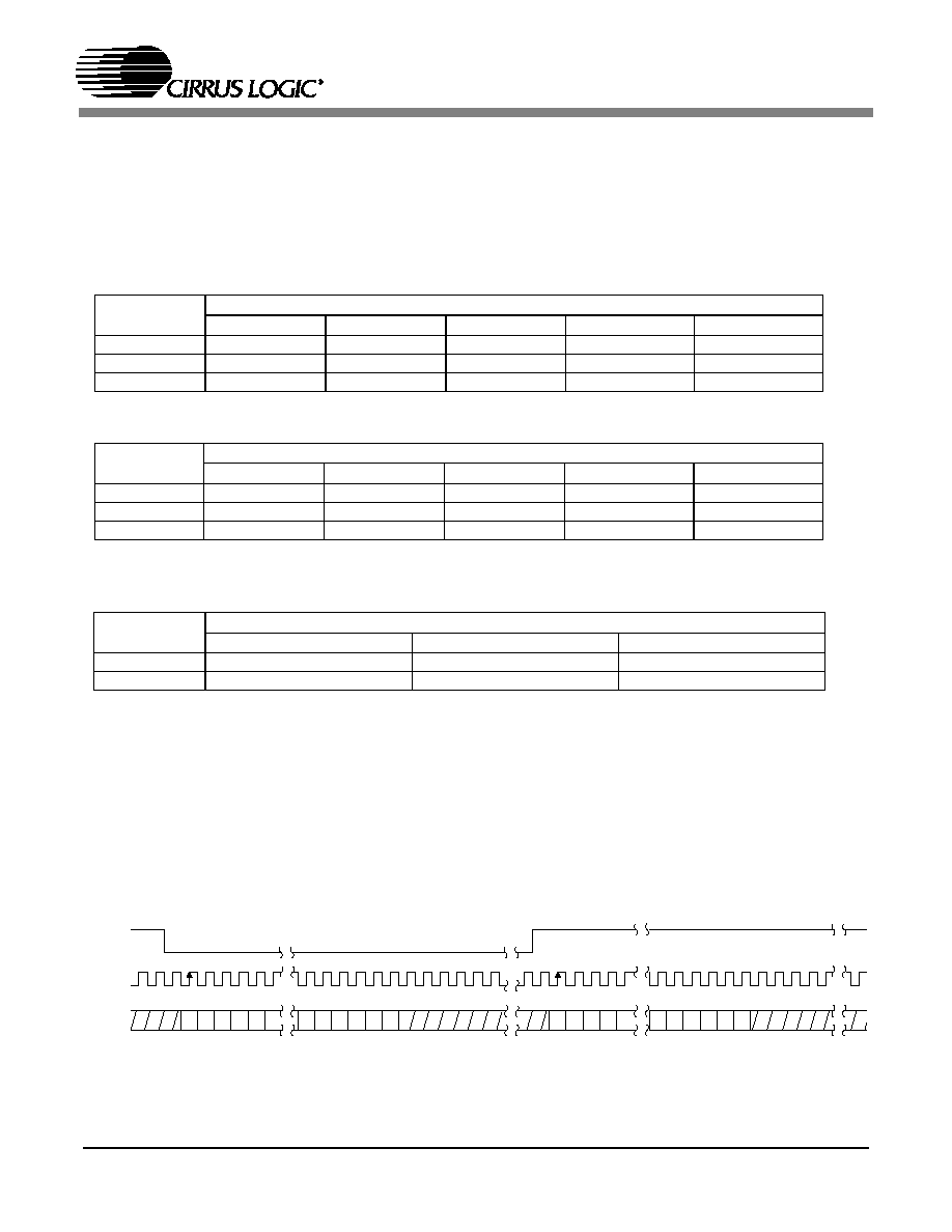
Sample Rate
(kHz)
MCLK (MHz)
256x
384x
512x
768x
1024x*
32
8.1920
12.2880
16.3840
24.5760
32.7680
44.1
11.2896
16.9344
22.5792
33.8688
45.1584
48
12.2880
18.4320
24.5760
36.8640
49.1520
Table 3. Single-Speed Mode Standard Frequencies
Sample Rate
(kHz)
MCLK (MHz)
128x
192x
256x
384x
512x*
64
8.1920
12.2880
16.3840
24.5760
32.7680
88.2
11.2896
16.9344
22.5792
33.8688
45.1584
96
12.2880
18.4320
24.5760
36.8640
49.1520
Table 4. Double-Speed Mode Standard Frequencies
Sample Rate
(kHz)
MCLK (MHz)
128x
192x
256x*
176.4
22.5792
33.8688
45.1584
192
24.5760
36.8640
49.1520
Table 5. Quad-Speed Mode Standard Frequencies
L R C K
S C L K
Le ft C h a nn el
R ig h t C ha n ne l
S D IN
+ 3 + 2 + 1
+ 5 + 4
M S B
-1 -2 -3 -4 -5
+ 3 + 2 + 1
+ 5 + 4
-1 -2 -3 -4
M S B
LS B
LS B
Figure 2. I
2
S Data

CS4341A
DS582PP1
9
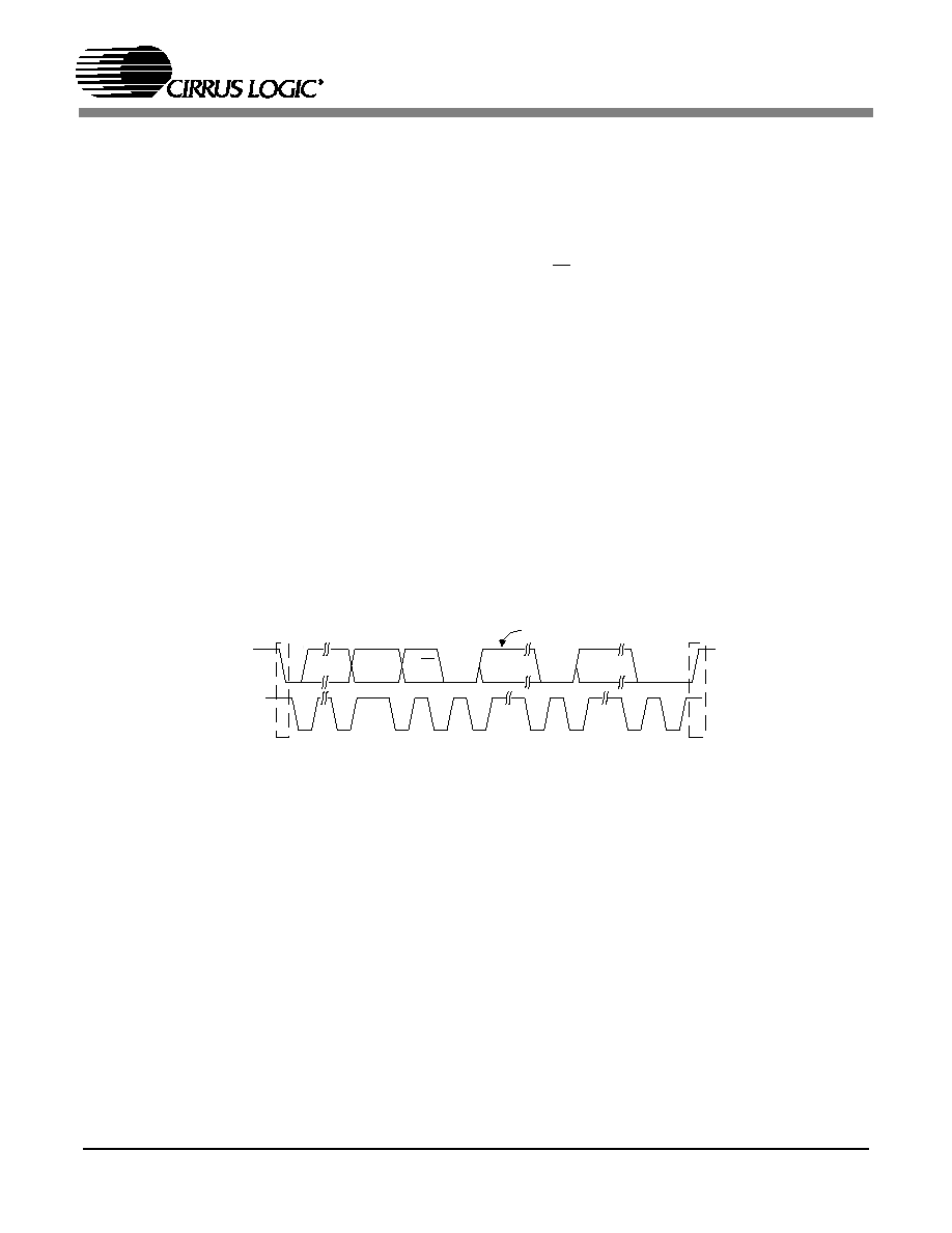
3.5
De-Emphasis Control
The device includes on-chip digital de-emphasis. The Mode Control 2 bits select either the 32, 44.1, or 48
kHz de-emphasis filter. Figure 5 shows the de-emphasis curve for F
s
equal to 44.1 kHz. The frequency
response of the de-emphasis curve will scale proportionally with changes in sample rate, Fs. Please see
section 5.2.3 for the desired de-emphasis control.
NOTE: De-emphasis is only available in Single-Speed Mode.
3.6
Recommended Power-up Sequence
1. Hold RST low until the power supply is stable, and the master and left/right clocks are locked to
the appropriate frequences, as discussed in section 3.2. In this state, the control port is reset to its
default settings and VQ will remain low.
2. Bring RST high. The device will remain in a low power state with VQ low.
3. Load the desired register settings while keeping the PDN bit set to 1.
4. Set the PDN bit to 0. This will initiate the power-up sequence, which lasts approximatel y 50µS
when the POR bit is set to 0. If the POR bit is set to 1, see section 3.7 for a complete description
of power-up timing.
L R C K
S C L K
L e ft C h a n n e l
R ig h t C h a n n e l
S D IN
+ 3 + 2 + 1
+ 5 + 4
M S B
-1 -2 -3 -4 -5
+ 3 + 2 + 1
+ 5 + 4
-1 -2 -3 -4
L S B
M S B
L S B
Figure 3. Left Justified up to 24-Bit Data
L R C K
S C L K
L e ft C h a n n e l
S D IN
-6 -5
-4 -3 -2 -1
-7
+ 1 + 2 + 3 + 4 + 5
3 2 c lo c k s
M SB
R ig h t C h a n n e l
L S B
M SB
+ 1 + 2 + 3 + 4 + 5
L S B
-6 -5
-4 -3 -2 -1
-7
M SB
Figure 4. Right Justified Data
G a in
d B
-1 0d B
0dB
F re q u e n c y
T 2 = 15 µ s
T 1= 50 µ s
F 1
F2
3.183 kH z
10 .61 kH z
Figure 5. De-Emphasis Curve

CS4341A
10
DS582PP1
3.7
Popguard
Æ
Transient Control
The CS4341A uses Popguard
Æ
technology to minimize the effects of output transients during power-up
and power-down. This technology, when used with external DC-blocking capacitors in series with the au-
dio outputs, minimizes the audio transients commonly produced by single-ended single-supply converters.
It is activated inside the DAC when the PDN bit or the RST pin is enabled/disabled and requires no other
external control, aside from choosing the appropriate DC-blocking capacitors.
3.7.1
Power-up
When the device is initially powered-up, the audio outputs, AOUTL and AOUTR, are clamped to
AGND. Following a delay of approximately 1000 sample periods, each output begins to ramp to-
ward the quiescent voltage. Approximately 10,000 LRCK cycles later, the outputs reach V
Q
and
audio output begins. This gradual voltage ramping allows time for the external DC-blocking capac-
itors to charge to the quiescent voltage, minimizing the power-up transient.
3.7.2
Power-down
To prevent transients at power-down, the device must first enter its power-down state by enabling
RST or PDN. When this occurs, audio output ceases and the internal output buffers are disconnect-
ed from AOUTL and AOUTR. In their place, a soft-start current sink is substituted which allows
the DC-blocking capacitors to slowly discharge. Once this charge is dissipated, the power to the
device may be turned off and the system is ready for the next power-on.
3.7.3
Discharge Time
To prevent an audio transient at the next power-on, it is necessary to ensure that the DC-blocking
capacitors have fully discharged before turning on the power or exiting the power-down state. If
not, a transient will occur when the audio outputs are initially clamped to AGND. The time that the
device must remain in the power-down state is related to the value of the DC-blocking capacitance.
For example, with a 3.3 µF capacitor, the minimum power-down time will be approximately 0.4
seconds.
3.8
Grounding and Power Supply Arrangements
As with any high resolution converter, the CS4341A requires careful attention to power supply and
grounding arrangements if its potential performance is to be realized. Figure 1 shows the recommended
power arrangements, with VA connected to a clean supply. If the ground planes are split between digital
ground and analog ground, REF_GND & AGND should be connected to the analog ground plane.
Decoupling capacitors should be as close to the DAC as possible, with the low value ceramic capacitor
being the closest. To further minimze impedance, these capacitors should be located on the same layer as
the DAC.
All signals, especially clocks, should be kept away from the FILT+ and VQ pins in order to avoid unwant-
ed coupling into the modulators. The FILT+ and VQ decoupling capacitors, particularly the 0. 1µF, must
be positioned to minimize the electrical path from FILT+ to REF_GND (and VQ to REF_GND), and
should also be located on the same layer as the DAC. The CDB4341A evaluation board demonstrates the
optimum layout and power supply arrangements.

CS4341A
DS582PP1
11
3.9
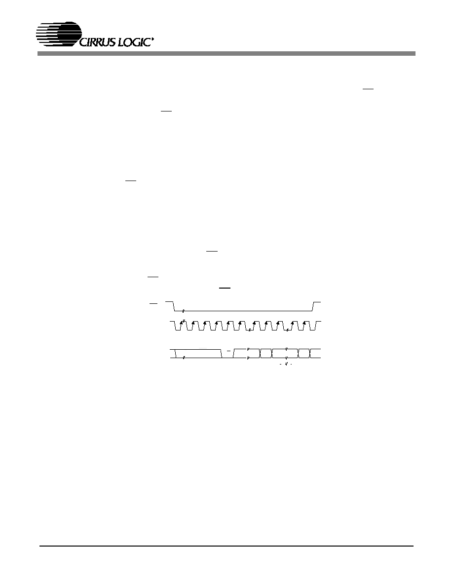
Control Port Interface
The control port is used to load all the internal register settings (see section 5). The operation of the control
port may be completely asynchronous with the audio sample rate. However, to avoid potential interference
problems, the control port pins should remain static if no operation is required.
The control port operates in one of two modes: I
2
C or SPI.
Notes: MCLK must be applied during all I
2
C communication.
3.9.1
MAP Auto Increment
The device has MAP (memory address pointer) auto increment capability enabled by the INCR bit
(also the MSB) of the MAP. If INCR is set to 0, MAP will stay constant for successive I
2
C writes
or reads, and SPI writes. If INCR is set to 1, MAP will auto increment after each byte is written,
allowing block reads or writes of successive registers.
3.9.2
I
2
C Mode
In the I
2
C mode, data is clocked into and out of the bi-directional serial control data line, SDA, by
the serial control port clock, SCL (see Figure 6 for the clock to data relationship). There is no CS
pin. Pin AD0 enables the user to alter the chip address (001000[AD0][R/W]) and should be tied to
VA or GND as required, before powering up the device. If the device ever detects a high to low
transition on the AD0/CS pin after power-up, SPI mode will be selected.
3.9.2a
I
2
C Write
To write to the device, follow the procedure below while adhering to the control port
Switching Specifications in section 7.
1) Initiate a START condition to the I
2
C bus followed by the address byte. The upper 6 bits
must be 001000. The seventh bit must match the setting of the AD0 pin, and the eighth must
be 0. The eighth bit of the address byte is the R/W bit.
2) Wait for an acknowledge (ACK) from the part, then write to the memory address pointer,
MAP. This byte points to the register to be written.
3) Wait for an acknowledge (ACK) from the part, then write the desired data to the register
pointed to by the MAP.
4) If the INCR bit (see section 3.9.1) is set to 1, repeat the previous step until all the desired
registers are written, then initiate a STOP condition to the bus.
5) If the INCR bit is set to 0 and further I
2
C writes to other registers are desired, it is nec-
essary to initiate a repeated START condition and follow the procedure detailed from step
1. If no further writes to other registers are desired, initiate a STOP condition to the bus.
CS4341A
12
DS582PP1
3.9.2b
I
2
C Read
To read from the device, follow the procedure below while adhering to the control port
Switching Specifications.
1) Initiate a START condition to the I
2
C bus followed by the address byte. The upper 6 bits
must be 001000. The seventh bit must match the setting of the AD0 pin, and the eighth must
be 1. The eighth bit of the address byte is the R/W bit.
2) After transmitting an acknowledge (ACK), the device will then transmit the contents of
the register pointed to by the MAP. The MAP register will contain the address of the last
register written to the MAP, or the default address (see section 8.3) if an I
2
C read is the first
operation performed on the device.
3) Once the device has transmitted the contents of the register pointed to by the MAP, issue
an ACK.
4) If the INCR bit is set to 1, the device will continue to transmit the contents of successive
registers. Continue providing a clock and issue an ACK after each byte until all the desired
registers are read, then initiate a STOP condition to the bus.
5) If the INCR bit is set to 0 and further I
2
C reads from other registers are desired, it is nec-
essary to initiate a repeated START condition and follow the procedure detailed from step
1. If no further reads from other registers are desired, initiate a STOP condition to the bus.
S D A
S C L
0 01 000
A D 0
R /W
S ta rt
A C K
D A T A
1-8
A C K
DA T A
1-8
A C K
Sto p
N O TE
N O TE: If o pe ration is a w rite, this byt e co ntains th e M e mory A ddr ess Poi n t er, MAP. If
op era tion is a rea d, this byte con tains the da ta of t h e r egis te r po in ted t o by t h e MAP.
Figure 6. Control Port Timing, I
2
C Mode
CS4341A
DS582PP1
13
3.9.3
SPI Mode
In SPI mode, data is clocked into the serial control data line, CDIN, by the serial control port clock,
CCLK (see Figure 7 for the clock to data relationship). There is no AD0 pin. Pin CS is the chip
select signal and is used to control SPI writes to the control port. When the device detects a high to
low transition on the AD0/CS pin after power-up, SPI mode will be selected. All signals are inputs
and data is clocked in on the rising edge of CCLK.
3.9.3a
SPI Write
To write to the device, follow the procedure below while adhering to the control port
Switching Specifications in section 6.
1) Bring CS low.
2) The address byte on the CDIN pin must then be 00100000.
3) Write to the memory address pointer, MAP. This byte points to the register to be written.
4) Write the desired data to the register pointed to by the MAP.
5) If the INCR bit (see section 3.9.1) is set to 1, repeat the previous step until all the desired
registers are written, then bring CS high.
6) If the INCR bit is set to 0 and further SPI writes to other registers are desired, it is nec-
essary to bring CS high, and follow the procedure detailed from step 1. If no further writes
to other registers are desired, bring CS high.
M A P
MSB
L S B
DATA
byte 1
byte n
R/W
M A P = M em ory A ddress Pointe r
ADDRESS
C H IP
C D IN
C C LK
CS
0 0 1 0 0 0 0
Figure 7. Control Port Timing, SPI mode

CS4341A
14
DS582PP1
3.10
Memory Address Pointer (MAP)
4.
REGISTER QUICK REFERENCE
Addr
Function
7
6
5
4
3
2
1
0
0h
Mode Control 1
Reserved
MC1
MC0
Reserved
Reserved
AUTOD
MCLKDIV
Reserved
DEFAULT
0
0
0
0
0
0
0
0
1h
Mode Control 2
AMUTE
DIF2
DIF1
DIF0
DEM1
DEM1
POR
PDN
DEFAULT
1
0
0
0
0
0
1
1
2h
Transition and Mixing
Control
A = B
SOFT
ZERO
CROSS
ATAPI4
ATAPI3
ATAPI2
ATAPI1
ATAPI0
DEFAULT
0
0
0
0
0
0
0
0
3h
Channel A Volume
Control
MUTEA
VOLA6
VOLA5
VOLA4
VOLA3
VOLA2
VOLA1
VOLA0
DEFAULT
0
0
0
0
0
0
0
0
4h
Channel B Volume
Control
MUTEB
VOLB6
VOLB5
VOLB4
VOLB3
VOLB2
VOLB1
VOLB0
DEFAULT
0
0
0
0
0
0
0
0
3.10.1 INCR (AUTO MAP INCREMENT ENABLE)
Default = `0'
0 - Disabled
1 - Enabled
3.10.2 MAP (MEMORY ADDRESS POINTER)
Default = `000'
7
6
5
4
3
2
1
0
INCR
Reserved
Reserved
Reserved
Reserved
MAP2
MAP1
MAP0
0
0
0
0
0
0
0
0

CS4341A
DS582PP1
15
5.
REGISTER DESCRIPTION
NOTE: All registers are read/write in I
2
C mode and write only in SPI mode, unless otherwise stated.
5.1
MODE CONTROL 1 (ADDRESS 00H)
5.1.1 SPEED MODE CONTROL (MC)
BIT 5-6
Default = 00
00 - Single-Speed Mode
01 - Double-Speed Mode
10 - Quad-Speed Mode
The operational speed mode must be set if the auto-detect defeat bit is enabled (AUTOD = 1). These
bits are ignored if the auto-detect defeat is disabled (AUTOD = 0).
5.1.2 AUTO-DETECT DEFEAT (AUTOD)
BIT 2
Default = 0
0 - Disabled
1 - Enabled
The Auto-Detect function can be defeated to allow sample rate changes from 50 to 84 kHz, and from
100 to 170 kHz. The operational speed mode must be set via the speed mode control bits (see section
5.1.1) if the auto-detect feature is defeated.
5.1.3 MCLK DIVIDE-BY-2 (MCLKDIV)
BIT 1
Default = 0
0 - Disabled
1 - Enabled
Function:
The MCLKDIV bit enables a circuit which divides the externally applied MCLK signal by 2.
5.2
MODE CONTROL 2 (ADDRESS 01H)
7
6
5
4
3
2
1
0
Reserved
MC1
MC0
Reserved
Reserved
AUTOD
MCLKDIV
Reserved
0
0
0
0
0
0
0
0
7
6
5
4
3
2
1
0
AMUTE
DIF2
DIF1
DIF0
DEM1
DEM0
POR
PDN
1
0
0
0
0
0
1
1
CS4341A
16
DS582PP1
5.2.1 AUTO-MUTE (AMUTE)
BIT 7
Default = 1
0 - Disabled
1 - Enabled
Function:
The Digital-to-Analog converter output will mute following the reception of 8192 consecutive audio
samples of static 0 or -1. A single sample of non-zero data will release the mute. Detection and mut-
ing is done independently for each channel. The quiescent voltage on the output will be retained and
the Mute Control pin will go active during the mute period. The muting function is affected, similiar to
volume control changes, by the Soft and Zero Cross bits in the Transition and Mixing Control (address
02h) register.
5.2.2 DIGITAL INTERFACE FORMAT (DIF)
BIT 4-6
Default = 000 - Format 0 (I
2
S, up to 24-bit data)
Function:
The required relationship between the Left/Right clock, serial clock and serial data is defined by the
Digital Interface Format and the options are detailed in Figures 2-4.
5.2.3 DE-EMPHASIS CONTROL (DEM)
BIT 2-3
Default = 00
00 - Disabled
01 - 44.1 kHz
10 - 48 kHz
11 - 32 kHz
Function:
Implementation of the standard 15
µ
s/50
µ
s digital de-emphasis filter response, Figure 5, requires re-
configuration of the digital filter to maintain the proper filter response for 32, 44.1 or 48 kHz sample
rates.
NOTE: De-emphasis is only available in Single-Speed Mode.
DIF2
DIF1
DIF0
DESCRIPTION
Format
FIGURE
0
0
0
I
2
S, up to 24-bit data
1
2
0
0
1
Identical to Format 1
1
2
0
1
0
Left Justified, up to 24-bit data,
2
3
0
1
1
Right Justified, 24-bit data
3
4
1
0
0
Right Justified, 20-bit data
4
4
1
0
1
Right Justified, 16-bit data
5
4
1
1
0
Right Justified, 18-bit data
6
4
1
1
1
Identical to Format 1
1
2
Table 6. Digital Interface Format
CS4341A
DS582PP1
17
5.2.4 POPGUARD
Æ
TRANSIENT CONTROL (POR)
BIT 1
Default = 1
0 - Disabled
1 - Enabled
Function:
The PopGuard
Æ
Transient Control allows the quiescent voltage to slowly ramp to and from 0 volts to
the quiescent voltage during power-on or power-down. Please refer to section 3.7 for implementation
details.
5.2.5 POWER DOWN (PDN)
BIT 0
Default = 1
0 - Disabled
1 - Enabled
Function:
The device will enter a low-power state when this function is enabled. The power-down bit defaults to
`enabled' on power-up and must be disabled before normal operation can occur. The contents of the
control registers are retained in this mode.
5.3
TRANSITION AND MIXING CONTROL (ADDRESS 02H)
5.3.1 CHANNEL A VOLUME = CHANNEL B VOLUME (A = B)
BIT 7
Default = 0
0 - Disabled
1 - Enabled
Fucntion:
The AOUTA and AOUTB volume levels are independently controlled by the A and the B Channel Vol-
ume Control Bytes when this function is disabled. The volume on both AOUTA and AOUTB are de-
termined by the A Channel Volume Control Byte and the B Channel Byte is ignored when this function
is enabled.
7
6
5
4
3
2
1
0
A = B
SZC1
SZC0
ATAPI4
ATAPI3
ATAPI2
ATAPI1
ATAPI0
0
1
0
0
1
0
0
1
CS4341A
18
DS582PP1
5.3.2 SOFT RAMP AND ZERO CROSS CONTROL (SZC)
BIT 5-6
Default = 10
00 - Immediate Changes
01 - Changes On Zero Crossings
10 - Soft Ramped Changes
11 - Soft Ramped Changes On Zero Crossings
Fucntion:
Immediate Changes
When Immediate Changes is selected all level changes will take effect immediately in one step.
Changes On Zero Crossings
Changes on Zero Crossings dictates that signal level changes, either by attenuation changes or mut-
ing, will occur on a signal zero crossing to minimize audible artifacts. The requested level change will
occur after a timeout period between 512 and 1024 sample periods (10.7 ms to 21.3 ms at 48 kHz
sample rate) if the signal does not encounter a zero crossing. The zero cross function is independent-
tly monitored and implemented for each channel.
Soft Ramped Changes
Soft Ramped Changes allows level changes, both muting and attenuation, to be implemented by in-
crementally ramping, in 1/8 dB steps, from the current level to the new level at a rate of 1dB per 8
left/right clock periods.
Soft Ramped Changes on Zero Crossings
Soft Ramped Changes On Zero Crossings dictates that signal level changes, either by attenuation
changes or muting, will occur in 1/8 dB steps implemented on a signal zero crossing. The 1/8 dB level
change will occur after a timeout period between 512 and 1024 sample periods (10.7 ms to 21.3 ms
at 48 kHz sample rate) if the signal does not encounter a zero crossing. The zero cross function is
indepently monitored and implemented for each channel.
5.3.3 ATAPI CHANNEL MIXING AND MUTING (ATAPI)
BIT 0-4
Default = 01001 - AOUTA = Left Channel, AOUTB = Right Channel (Stereo)
Fucntion:
The CS4341A implements the channel mixing functions of the ATAPI CD-ROM specification. Refer
to Table 7 and Figure 8 for additional information.
ATAPI4
ATAPI3
ATAPI2
ATAPI1
ATAPI0
AOUTA
AOUTB
0
0
0
0
0
MUTE
MUTE
0
0
0
0
1
MUTE
bR
0
0
0
1
0
MUTE
bL
0
0
0
1
1
MUTE
b[(L+R)/2]
0
0
1
0
0
aR
MUTE
0
0
1
0
1
aR
bR
0
0
1
1
0
aR
bL
0
0
1
1
1
aR
b[(L+R)/2]
0
1
0
0
0
aL
MUTE
0
1
0
0
1
aL
bR
Table 7. ATAPI Decode

CS4341A
DS582PP1
19
0
1
0
1
0
aL
bL
0
1
0
1
1
aL
b[(L+R)/2]
0
1
1
0
0
a[(L+R)/2]
MUTE
0
1
1
0
1
a[(L+R)/2]
bR
0
1
1
1
0
a[(L+R)/2]
bL
0
1
1
1
1
a[(L+R)/2]
b[(L+R)/2]
1
0
0
0
0
MUTE
MUTE
1
0
0
0
1
MUTE
bR
1
0
0
1
0
MUTE
bL
1
0
0
1
1
MUTE
[(aL+bR)/2]
1
0
1
0
0
aR
MUTE
1
0
1
0
1
aR
bR
1
0
1
1
0
aR
bL
1
0
1
1
1
aR
[(bL+aR)/2]
1
1
0
0
0
aL
MUTE
1
1
0
0
1
aL
bR
1
1
0
1
0
aL
bL
1
1
0
1
1
aL
[(aL+bR)/2]
1
1
1
0
0
[(aL+bR)/2]
MUTE
1
1
1
0
1
[(aL+bR)/2]
bR
1
1
1
1
0
[(bL+aR)/2]
bL
1
1
1
1
1
[(aL+bR)/2]
[(aL+bR)/2]
ATAPI4
ATAPI3
ATAPI2
ATAPI1
ATAPI0
AOUTA
AOUTB
Table 7. ATAPI Decode (Continued)
A C h an nel
V olum e
C o ntro l
Ao utA
Ao utB
L eft C han nel
A ud io D ata
R ig ht C ha nne l
A ud io D ata
B C h an ne l
V o lu m e
C o ntro l
M U TE
M U TE
Figure 8. ATAPI Block Diagram

CS4341A
20
DS582PP1
5.4
CHANNEL A VOLUME CONTROL (ADDRESS 03H)
5.5
CHANNEL B VOLUME CONTROL (ADDRESS 04H)
5.5.1 MUTE (MUTE)
BIT 7
Default = 0
0 - Disabled
1 - Enabled
Fucntion:
The Digital-to-Analog converter output will mute when enabled. The quiescent voltage on the output
will be retained. The muting function is affected, similiar to attenuation changes, by the Soft and Zero
Cross bits in the Transition and Mixing Control (address 02h) register. The MUTEC will go active dur-
ing the mute period if the Mute function is enabled for both channels.
5.5.2 VOLUME (VOLx)
BIT 0-6
Default = 0 dB (No Attenuation)
Function:
The digital volume control allows the user to attenuate the signal in 1 dB increments from 0 to -90 dB.
Volume settings are decoded as shown in Table 8. The volume changes are implemented as dictated
by the Soft and Zero Cross bits in the Transition and Mixing Control (address 02h) register. All volume
settings less than - 94 dB are equivalent to enabling the Mute bit.
7
6
5
4
3
2
1
0
MUTEx
VOLx6
VOLx5
VOLx4
VOLx3
VOLx2
VOLx1
VOLx0
0
0
0
0
0
0
0
0
Binary Code
Decimal Value
Volume Setting
0000000
0
0 dB
0010100
20
-20 dB
0101000
40
-40 dB
0111100
60
-60 dB
1011010
90
-90 dB
Table 8. example Digital Volume Settings

CS4341A
DS582PP1
21
6. CHARACTERISTICS AND SPECIFICATIONS
ANALOG CHARACTERISTICS (CS4341A-KS)
(Test conditions (unless otherwise specified):
Input test signal is a 997 Hz sine wave at 0 dBFS; measurement bandwidth is 10 Hz to 20 kHz; test load R
L
=
10k
, C
L
= 10 pF (see Figure 9). Typical performance characteristics are derived from measurements taken at
T
A
= 25
∞
C, VA = 5.0V and 3.3V. Min/Max performance characteristics are guaranteed over the specified operating
temperature and voltages.
)
Parameter
VA = 5.0V
VA = 3.3V
Min
Typ
Max
Min
Typ
Max
Unit
Single-Speed Mode Fs = 48kHz
Dynamic Range
(Note 1)
18 to 24-Bit
unweighted
A-Weighted
16-Bit
unweighted
A-Weighted
92
95
-
-
98
101
92
95
-
-
-
-
88
91
-
-
94
97
92
95
-
-
-
-
dB
dB
dB
dB
Total Harmonic Distortion + Noise
(Note 1)
18 to 24-Bit
0 dB
-20 dB
-60 dB
16-Bit
0 dB
-20 dB
-60 dB
-
-
-
-
-
-
-91
-78
-38
-90
-72
-32
-85
-
-
-
-
-
-
-
-
-
-
-
-94
-74
-34
-91
-72
-32
-88
-
-
-
-
-
dB
dB
dB
dB
dB
dB
Double-Speed Mode Fs = 96kHz
Dynamic Range
(Note 1)
18 to 24-Bit
unweighted
A-Weighted
16-Bit
unweighted
A-Weighted
92
95
-
-
98
101
92
95
-
-
-
-
88
91
-
-
94
97
92
95
-
-
-
-
dB
dB
dB
dB
Total Harmonic Distortion + Noise
(Note 1)
18 to 24-Bit
0 dB
-20 dB
-60 dB
16-Bit
0 dB
-20 dB
-60 dB
-
-
-
-
-
-
-91
-78
-38
-90
-72
-32
-85
-
-
-
-
-
-
-
-
-
-
-
-94
-74
-34
-91
-72
-32
-88
-
-
-
-
-
dB
dB
dB
dB
dB
dB
Quad-Speed Mode Fs = 192kHz
Dynamic Range
(Note 1)
18 to 24-Bit
unweighted
A-Weighted
16-Bit
unweighted
A-Weighted
92
95
-
-
98
101
92
95
-
-
-
-
88
91
-
-
94
97
92
95
-
-
-
-
dB
dB
dB
dB
Total Harmonic Distortion + Noise
(Note 1)
18 to 24-Bit
0 dB
-20 dB
-60 dB
16-Bit
0 dB
-20 dB
-60 dB
-
-
-
-
-
-
-91
-78
-38
-90
-72
-32
-85
-
-
-
-
-
-
-
-
-
-
-
-94
-74
-34
-91
-72
-32
-88
-
-
-
-
-
dB
dB
dB
dB
dB
dB
CS4341A
22
DS582PP1
ANALOG CHARACTERISTICS (CS4341A-KS)
(Continued)
Notes: 1. One-half LSB of triangular PDF dither is added to data.
2. Refer to Figure 10.
.
Parameters
Symbol
Min
Typ
Max
Units
Dynamic Performance for All Modes
Interchannel Isolation (1 kHz)
-
102
-
dB
DC Accuracy
Interchannel Gain Mismatch
-
0.1
-
dB
Gain Drift
-
±100
-
ppm/∞C
Analog Output Characteristics and Specifications
Full Scale Output Voltage
0.6∑VA
0.7∑VA
0.8∑VA
Vpp
Output Impedance
-
100
-
Minimum AC-Load Resistance
(Note 2)
R
L
-
3
-
k
Maximum Load Capacitance
(Note 2)
C
L
-
100
-
pF
A O UT x
AG N D
3.3 µF
V
ou t
R
L
C
L
+
Figure 9. Output Test Load
1 0 0
5 0
7 5
2 5
2 .5
5
1 0
15
S a fe O p e ra tin g
R e g io n
C
a
p
a
c
i
t
i
v
e
Load -
-
C
(
p
F
)
L
R e s is tiv e L o a d -- R (k
)
L
1 2 5
3
2 0
Figure 10. Maximum Loading
CS4341A
DS582PP1
23
COMBINED INTERPOLATION & ON-CHIP ANALOG FILTER RESPONSE
(The
filter characteristics and the X-axis of the response plots have been normalized to the sample rate (Fs) and can be
referenced to the desired sample rate by multiplying the given characteristic by Fs.)
Notes: 3. For Single-Speed Mode, the measurement bandwidth is 0.5465 Fs to 3 Fs.
For Double-Speed Mode, the measurement bandwidth is 0.577 Fs to 1.4 Fs.
4. De-emphasis is only available in Single-Speed Mode.
Parameter
Min
Typ
Max
Unit
Single-Speed Mode - (4kHz to 50kHz sample rates)
Passband
to -0.05 dB corner
to -3 dB corner
0
0
-
-
0.4535
0.4998
Fs
Fs
Frequency Response 10 Hz to 20 kHz
-0.02
-
+0.08
dB
StopBand
0.5465
-
-
Fs
StopBand Attenuation
(Note 3)
50
-
-
dB
Group Delay
-
9/Fs
-
s
Passband Group Delay Deviation
0 - 20 kHz
-
±0.36/Fs
-
s
De-emphasis Error (Relative to 1 kHz)
Fs = 32 kHz
(Note 4)
Fs = 44.1 kHz
Fs = 48 kHz
-
-
-
-
-
-
+0.2/-0.1
+0.05/-0.14
+0/-0.22
dB
dB
dB
Double-Speed Mode - (50kHz to 100kHz sample rates)
Passband
to -0.1 dB corner
to -3 dB corner
0
0
-
-
0.4621
0.4982
Fs
Fs
Frequency Response 10 Hz to 20 kHz
-0.06
-
+0.2
dB
StopBand
0.577
-
-
Fs
StopBand Attenuation
(Note 3)
55
-
-
dB
Group Delay
-
4/Fs
-
s
Passband Group Delay Deviation
0 - 40 kHz
0 - 20 kHz
-
-
±1.39/Fs
±0.23/Fs
-
-
s
s
Quad-Speed Mode - (100kHz to 200kHz sample rates)
Frequency Response 10 Hz to 20 kHz
-1
-
0
dB
Group Delay
-
3/Fs
-
s
CS4341A
24
DS582PP1
Figure 11. Single-Speed Stopband Rejection
Figure 12. Single-Speed Transition Band
Figure 13. Single-Speed Transition Band (Detail)
Figure 14. Single-Speed Passband Ripple
Figure 15. Double-Speed Stopband Rejection
Figure 16. Double-Speed Transition Band

CS4341A
DS582PP1
25
Figure 17. Double-Speed Transition Band (Detail)
Figure 18. Double-Speed Passband Ripple

CS4341A
26
DS582PP1
SWITCHING SPECIFICATIONS - SERIAL AUDIO INTERFACE
Parameters
Symbol Min
Max
Units
MCLK Frequency
1.024
51.2
MHz
MCLK Duty Cycle
45
55
%
Input Sample Rate
Single-Speed Mode
Double-Speed Mode
Quad-Speed Mode
Fs
Fs
Fs
4
50
100
50
100
200
kHz
kHz
kHz
LRCK Duty Cycle
40
60
%
SCLK Pulse Width Low
t
sclkl
20
-
ns
SCLK Pulse Width High
t
sclkh
20
-
ns
SCLK Frequency
MCLKDIV Disabled
-
Hz
MCLKDIV Enabled
-
Hz
SCLK rising to LRCK edge delay
t
slrd
20
-
ns
SCLK rising to LRCK edge setup time
t
slrs
20
-
ns
SDIN valid to SCLK rising setup time
t
sdlrs
20
-
ns
SCLK rising to SDIN hold time
t
sdh
20
-
ns
sclkh
t
slrs
t
slrd
t
sdlrs
t
sdh
t
sclkl
t
S D IN
S C LK
LR C K
Figure 19. Serial Input Timing
MCLK
2
------------------
MCLK
4
------------------
CS4341A
DS582PP1
27
SWITCHING SPECIFICATIONS - CONTROL PORT INTERFACE
(Inputs: Logic
0 = AGND, Logic 1 = VA)
Notes: 5. Data must be held for sufficient time to bridge the transition time, t
fc
, of SCL.
Parameter
Symbol
Min
Max
Unit
I
2
C Mode
SCL Clock Frequency
f
scl
-
100
kHz
RST Rising Edge to Start
t
irs
500
-
ns
Bus Free Time Between Transmissions
t
buf
4.7
-
µs
Start Condition Hold Time (prior to first clock pulse)
t
hdst
4.0
-
µs
Clock Low time
t
low
4.7
-
µs
Clock High Time
t
high
4.0
-
µs
Setup Time for Repeated Start Condition
t
sust
4.7
-
µs
SDA Hold Time from SCL Falling
(Note 5)
t
hdd
0
-
µs
SDA Setup time to SCL Rising
t
sud
250
-
ns
Rise Time of SCL and SDA
t
rc
, t
rc
-
1
µs
Fall Time SCL and SDA
t
fc
, t
fc
-
300
ns
Setup Time for Stop Condition
t
susp
4.7
-
µs
t
b uf
t
h ds t
t
l o w
t
h dd
t
h ig h
t
s u d
S to p
S t a r t
S D A
S C L
t
irs
R S T
t
h ds t
t
rc
t
fc
t su st
t su sp
S t a r t
S to p
R e p e a t e d
t
rd
t
fd
t
a c k
Figure 20. Control Port Timing - I
2
C Mode
CS4341A
28
DS582PP1
SWITCHING SPECIFICATIONS - CONTROL PORT INTERFACE
(Continued)
Notes: 6. t
spi
only needed before first falling edge of CS after RST rising edge. t
spi
= 0 at all other times.
7. Data must be held for sufficient time to bridge the transition time of CCLK.
8. For f
sclk
< 1 MHz.
Parameter
Symbol
Min
Max
Unit
SPI Mode
CCLK Clock Frequency
f
sclk
-
6
MHz
RST Rising Edge to CS Falling
t
srs
500
-
ns
CCLK Edge to CS Falling
(Note 6)
t
spi
500
-
ns
CS High Time Between Transmissions
t
csh
1.0
-
µs
CS Falling to CCLK Edge
t
css
20
-
ns
CCLK Low Time
t
scl
66
-
ns
CCLK High Time
t
sch
66
-
ns
CDIN to CCLK Rising Setup Time
t
dsu
40
-
ns
CCLK Rising to DATA Hold Time
(Note 7)
t
dh
15
-
ns
Rise Time of CCLK and CDIN
(Note 8)
t
r2
-
100
ns
Fall Time of CCLK and CDIN
(Note 8)
t
f2
-
100
ns
t r2
t f2
t dsu t dh
t sch
t scl
C S
C C LK
C D IN
t css
t csh
t spi
t srs
R S T
Figure 21. Control Port Timing - SPI Mode

CS4341A
DS582PP1
29
DC ELECTRICAL CHARACTERISTICS
(AGND = 0V; all voltages with respect to AGND.)
DIGITAL INPUT CHARACTERISTICS
(AGND = 0V; all voltages with respect to AGND.)
DIGITAL INTERFACE SPECIFICATIONS
(GND = 0 V; all voltages with respect to GND.)
THERMAL CHARACTERISTICS AND SPECIFICATIONS
Parameters
Symbol
Min
Typ
Max
Units
Normal Operation
(Note 9)
Power Supply Current
VA = 5.0V
VA = 3.3V
I
A
-
-
18
15
25
20
mA
mA
Power Dissipation
VA = 5.0V
VA = 3.3V
-
-
90
50
125
100
mW
mW
Power-down Mode
(Note 10)
Power Supply Current
VA = 5.0V
VA
=
3.3V
I
A
-
-
60
35
-
-
µ
A
µ
A
Power Dissipation
VA = 5.0V
VA = 3.3V
-
-
0.3
0.1
-
-
mW
mW
All Modes of Operation
Power Supply Rejection Ratio
(Note 11)
1 kHz
60 Hz
PSRR
-
-
60
40
-
-
dB
dB
V
Q
Nominal Voltage
Output Impedance
Maximum allowable DC current source/sink
-
-
-
0.5∑VA
250
0.01
-
-
-
V
k
mA
Filt+ Nominal Voltage
Output Impedance
Maximum allowable DC current source/sink
-
-
-
VA
250
0.01
-
-
-
V
k
mA
MUTEC Low-Level Output Voltage
-
0
-
V
MUTEC High-Level Output Voltage
-
VA
-
V
Maximum MUTEC Drive Current
-
3
-
mA
Parameters
Symbol Min Typ
Max
Units
Input Leakage Current
I
in
-
-
±10
µ
A
Input Capacitance
-
8
-
pF
Parameters
Symbol Min Max
Units
Interface Voltage Supply = 3.3V or 5.0V
High-Level Input Voltage
V
IH
2.0
-
V
Low-Level Input Voltage
V
IL
-
0.8
V
Parameters
Symbol Min Typ
Max
Units
Package Thermal Resistance
JA
-
125
-
∞C/Watt
Ambient Operating Temperature
(Power Applied)
T
A
-10
-
+70
∞
C
CS4341A
30
DS582PP1
RECOMMENDED OPERATING SPECIFICATION
ABSOLUTE MAXIMUM RATINGS
(AGND = 0 V; all voltages with respect to AGND. Operation
beyond these limits may result in permanent damage to the device. Normal operation is not guaranteed at these
extremes.)
Notes: 9. Normal operation is defined as RST = HI with a 997 Hz, 0dBFS input sampled at the highest F
s
for each
speed mode, and open outputs, unless otherwise specified.
10. Power Down Mode is defined as RST = LO with all clocks and data lines held static.
11. Valid with the recommended capacitor values on FILT+ and VQ as shown in Figure 1. Increasing the
capacitance will also increase the PSRR.
12. Any pin except supplies.
Parameters
Symbol Min Typ
Max
Units
DC Power Supply
Analog
VA
2.7
4.5
3.3
5
3.6
5.5
V
V
Parameters
Symbol
Min
Max
Units
DC Power Supply
VA
-0.3
6.0
V
Input Current
(Note 12)
I
in
-
±10
mA
Digital Input Voltage
V
IND
-0.3
VA+0.4
V
Ambient Operating Temperature (power applied)
T
A
-55
125
∞C
Storage Temperature
T
stg
-65
150
∞C

CS4341A
DS582PP1
31
7.
PARAMETER DEFINITIONS
Total Harmonic Distortion + Noise (THD+N)
The ratio of the rms value of the signal to the rms sum of all other spectral components over the specified
bandwidth (typically 10Hz to 20kHz), including distortion components. Expressed in decibels.
Dynamic Range
The ratio of the full scale rms value of the signal to the rms sum of all other spectral components over the
specified bandwidth. Dynamic range is a signal-to-noise measurement over the specified bandwidth
made with a -60 dBFS signal. 60 dB is then added to the resulting measurement to refer the measurement
to full scale. This technique ensures that the distortion components are below the noise level and do not
affect the measurement. This measurement technique has been accepted by the Audio Engineering So-
ciety, AES17-1991, and the Electronic Industries Association of Japan, EIAJ CP-307.
Interchannel Isolation
A measure of crosstalk between the left and right channels. Measured for each channel at the converter's
output with all zeros to the input under test and a full-scale signal applied to the other channel. Units in
decibels.
Interchannel Gain Mismatch
The gain difference between left and right channels. Units in decibels.
Gain Error
The deviation from the nominal full scale analog output for a full scale digital input.
Gain Drift
The change in gain value with temperature. Units in ppm/∞C.
8.
REFERENCES
1) CDB4341A Evaluation Board Datasheet
2) "The I
2
C Bus Specification: Version 2.1" Philips Semiconductors, January 2000.
http://www.semiconductors.philips.com
CS4341A
32
DS582PP1
9.
PACKAGE DIMENSIONS
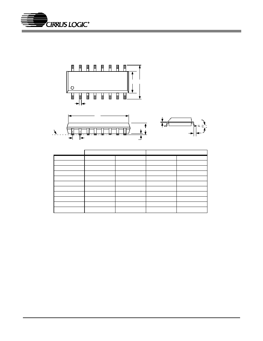
INCHES
MILLIMETERS
DIM
MIN
MAX
MIN
MAX
A 0.053
0.069
1.35
1.75
A1
0.004
0.010
0.10
0.25
B
0.013
0.020
0.33
0.51
C
0.007
0.010
0.19
0.25
D
0.386
0.394
9.80
10.00
E
0.150
0.157
3.80
4.00
e
0.040
0.060
1.02
1.52
H
0.228
0.244
5.80
6.20
L
0.016
0.050
0.40
1.27
0∞
8∞
0∞
8∞
JEDEC # : MS-012
e
16L SOIC (150 MIL BODY) PACKAGE DRAWING
D
H
E
b
A1
A
c
L
SEATING
PLANE
1