
Copyright
©
Cirrus Logic, Inc. 2005
(All Rights Reserved)
http://www.cirrus.com
Advance Product Information
This document contains information for a new product.
Cirrus Logic reserves the right to modify this product without notice.
CS4361
20-pin, 24-bit, 192 kHz, 6-channel D/A Converter
Features
Multi-bit Delta-sigma Modulator
24-bit Conversion
Automatically detects sample rates up to
192 kHz.
105 dB Dynamic Range
-95 dB THD+N
Low Clock Jitter Sensitivity
+3.3 V or +5 V Core Power
+1.8 V to +5 V Interface Power
Filtered Line Level Outputs
On-chip Digital De-emphasis
Popguard
TM
Technology
Mute Output Control
Small 20-pin TSSOP Package
Description
The CS4361 is a complete 6-channel digital-to-analog
output system including interpolation, multi-bit D/A
conversion, and output analog filtering in a small 20-pin
package. The CS4361 supports all major audio data
interface formats.
The CS4361 is based on a fourth order, multi-bit, delta-
sigma modulator with a linear analog low-pass filter. This
device also includes auto-speed mode detection using
both sample rate and master clock ratio as a method of
auto-selecting sampling rates between 2 kHz and
216 kHz.
The CS4361 contains on-chip digital de-emphasis, oper-
ates from a single +3.3 V or +5 V power supply with
separate built-in level shifter for the digital interface, and
requires minimal support circuitry. These features are
ideal for DVD players & recorders, digital televisions,
home theater and set top box products, and automotive
audio systems.
ORDERING INFORMATION
See page 20
I
Internal Voltage
Reference
+5 Volt-tolerant Reset
Auto-Speed
Detecting PCM Serial
Interface
L
e
vel
T
r
ansl
ator
Mode Control
Analog & Digital Core Supply
(3.3 V to 5 V)
Single-Ended
Outputs
(Six Channels)
6
PCM Serial
Audio Input
Digital
Filters
Switch-Cap
DAC and
Analog Filters
Multi-bit
Modulators
External Mute
Control
Mute Control
Serial Audio Port & Control Supply
(1.8 V to 5 V)
6
Digital
De-emphasis
JAN `05
DS672A2

CS4361
2
DS672A2
Table 1.
Revision History
Release
Date
Changes
A1
January 2005
Initial Release
A2
January 2005
Correction to PDF file size.
Contacting Cirrus Logic Support
For all product questions and inquiries contact a Cirrus Logic Sales Representative.
To find one nearest you go to www.cirrus.com
IMPORTANT NOTICE
"Advance" product information describes products that are in development and subject to development changes.
Cirrus Logic, Inc. and its subsidiaries ("Cirrus") believe that the information contained in this document is accurate and reliable. However, the information is subject
to change without notice and is provided "AS IS" without warranty of any kind (express or implied). Customers are advised to obtain the latest version of relevant
information to verify, before placing orders, that information being relied on is current and complete. All products are sold subject to the terms and conditions of sale
supplied at the time of order acknowledgment, including those pertaining to warranty, indemnification, and limitation of liability. No responsibility is assumed by
Cirrus for the use of this information, including use of this information as the basis for manufacture or sale of any items, or for infringement of patents or other rights
of third parties. This document is the property of Cirrus and by furnishing this information, Cirrus grants no license, express or implied under any patents, mask work
rights, copyrights, trademarks, trade secrets or other intellectual property rights. Cirrus owns the copyrights associated with the information contained herein and
gives consent for copies to be made of the information only for use within your organization with respect to Cirrus integrated circuits or other products of Cirrus. This
consent does not extend to other copying such as copying for general distribution, advertising or promotional purposes, or for creating any work for resale.
CERTAIN APPLICATIONS USING SEMICONDUCTOR PRODUCTS MAY INVOLVE POTENTIAL RISKS OF DEATH, PERSONAL INJURY, OR SEVERE PROP-
ERTY OR ENVIRONMENTAL DAMAGE ("CRITICAL APPLICATIONS"). CIRRUS PRODUCTS ARE NOT DESIGNED, AUTHORIZED OR WARRANTED FOR
USE IN AIRCRAFT SYSTEMS, MILITARY APPLICATIONS, PRODUCTS SURGICALLY IMPLANTED INTO THE BODY, AUTOMOTIVE SAFETY OR SECURITY
DEVICES, LIFE SUPPORT PRODUCTS OR OTHER CRITICAL APPLICATIONS. INCLUSION OF CIRRUS PRODUCTS IN SUCH APPLICATIONS IS UNDER-
STOOD TO BE FULLY AT THE CUSTOMER'S RISK AND CIRRUS DISCLAIMS AND MAKES NO WARRANTY, EXPRESS, STATUTORY OR IMPLIED, INCLUD-
ING THE IMPLIED WARRANTIES OF MERCHANTABILITY AND FITNESS FOR PARTICULAR PURPOSE, WITH REGARD TO ANY CIRRUS PRODUCT THAT
IS USED IN SUCH A MANNER. IF THE CUSTOMER OR CUSTOMER'S CUSTOMER USES OR PERMITS THE USE OF CIRRUS PRODUCTS IN CRITICAL
APPLICATIONS, CUSTOMER AGREES, BY SUCH USE, TO FULLY INDEMNIFY CIRRUS, ITS OFFICERS, DIRECTORS, EMPLOYEES, DISTRIBUTORS AND
OTHER AGENTS FROM ANY AND ALL LIABILITY, INCLUDING ATTORNEYS' FEES AND COSTS, THAT MAY RESULT FROM OR ARISE IN CONNECTION
WITH THESE USES.
Cirrus Logic, Cirrus, and the Cirrus Logic logo designs are trademarks of Cirrus Logic, Inc. All other brand and product names in this document may be trademarks
or service marks of their respective owners.

CS4361
DS672A2
3
TABLE OF CONTENTS
1. PIN DESCRIPTIONS ................................................................................................................ 4
2. CHARACTERISTICS AND SPECIFICATIONS ........................................................................ 5
Specified Operating Conditions ................................................................................................ 5
Absolute Maximum Ratings...................................................................................................... 5
DAC Analog Characteristics ..................................................................................................... 6
DAC Analog Characteristics - All Modes .................................................................................. 6
Combined Interpolation & On-chip Analog Filter Response ..................................................... 7
Digital Input Characteristics...................................................................................................... 8
Power & Thermal Characteristics ............................................................................................. 8
Switching Characteristics - Serial Audio Interface.................................................................... 9
3. TYPICAL CONNECTION DIAGRAM ..................................................................................... 11
4. APPLICATIONS ..................................................................................................................... 12
4.1 Master Clock .................................................................................................................... 12
4.2 Serial Clock ..................................................................................................................... 12
4.2.1 External Serial Clock Mode ................................................................................. 12
4.2.2 Internal Serial Clock Mode .................................................................................. 13
4.3 De-Emphasis ................................................................................................................... 15
4.4 Mode Select ..................................................................................................................... 15
4.5 Initialization and Power-Down ......................................................................................... 15
4.6 Output Transient Control ................................................................................................. 17
4.6.1 Power-up ............................................................................................................. 17
4.6.2 Power-down ........................................................................................................ 17
4.7 Grounding and Power Supply Decoupling ....................................................................... 17
4.8 Analog Output and Filtering ............................................................................................. 17
4.9 Mute Control .................................................................................................................... 18
5. PARAMETER DEFINITIONS .................................................................................................. 19
6. ORDERING INFORMATION .............................................................................................. 20
7. PACKAGE DIMENSIONS ...................................................................................................... 20
8. APPENDIX ......................................................................................................................... 21
CS4361
4
DS672A2
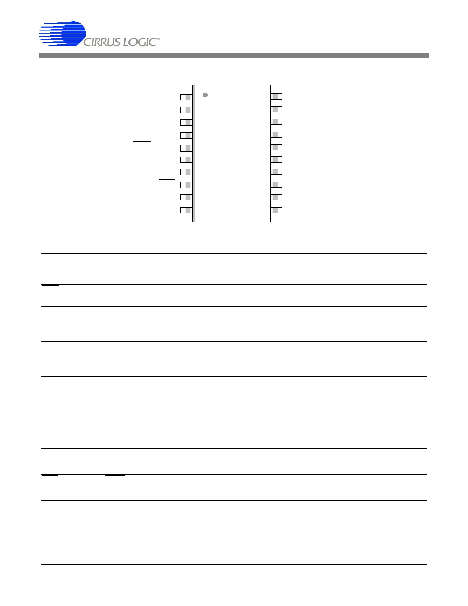
1. PIN DESCRIPTIONS
Pin Name
# Pin Description
SDIN1
SDIN2
SDIN3
2
3
4
Serial Audio Data Input (Input) - Input for two's complement serial audio data.
DEM/SCLK
5 De-emphasis/External Serial Clock Input (Input) - used for de-emphasis filter control or exter-
nal serial clock input.
LRCK
6 Left Right Clock (Input) - Determines which channel, Left or Right, is currently active on the
serial audio data line.
MCLK
7 Master Clock (Input) - Clock source for the delta-sigma modulator and digital filters.
VQ
11 Quiescent Voltage (Output) - Filter connection for internal quiescent voltage.
FILT+
10 Positive Voltage Reference (Output) - Positive reference voltage for the internal sampling
circuits.
AOUT1
AOUT2
AOUT3
AOUT4
AOUT5
AOUT6
19
18
17
16
13
12
Analog Output (Output) - The full scale analog output level is specified in the Analog Charac-
teristics specification table.
GND
14 Ground (Input) - ground reference.
VA
15 Analog Power (Input) - Positive power for the analog and core digital sections.
VL
1 Interface Power (Input) - Positive power for the digital interface level shifters.
RST
8 Reset (Input) - Applies reset to the internal circuitry when low.
MUTEC
20 Mute Control (Output) - Control signal for optional external muting circuitry.
MODE
9 Mode Control (Input) - Selects operational modes (see table 3).
VL
MUTEC
SDIN1
AOUT1
SDIN2
AOUT2
SDIN3
AOUT3
DEM/SCLK
AOUT4
LRCK
VA
MCLK
GND
RST
AOUT5
MODE
AOUT6
FILT+
VQ
1
2
3
4
5
16
17
18
19
20
6
7
8
9
10
11
12
13
14
15

CS4361
DS672A2
5
2.CHARACTERISTICS AND SPECIFICATIONS
All Min/Max characteristics and specifications are guaranteed over the specified operating conditions. Typical per-
formance characteristics and specifications are derived from measurements taken at nominal supply voltage and
T
A
= 25
∞
C.
SPECIFIED OPERATING CONDITIONS
AGND = 0 V; all voltages with respect to ground.
ABSOLUTE MAXIMUM RATINGS
AGND = 0 V; all voltages with respect to ground.
WARNING: Operation at or beyond these limits may result in permanent damage to the device. Normal operation is
not guaranteed at these extremes.
Parameters
Symbol Min Nom
Max
Units
DC Power Supply
VA
VA
VL
4.75
3.0
1.7
5.0
3.3
3.3
5.25
3.6
5.25
V
V
Specified Temperature Range
-CZZ
-DZZ
T
A
-10
-40
-
-
+70
+85
∞
C
∞
C
Parameters
Symbol
Min
Max
Units
DC Power Supply
VA
VL
-0.3
-0.3
6.0
VA
V
V
Input Current, Any Pin Except Supplies
I
in
-
±10
mA
Digital Input Voltage (pin 8, RST)
V
IND
-0.3
VA+0.4
V
Digital Input Voltage (all other digital pins)
V
IND
-0.3
VL+0.4
V
Ambient Operating Temperature (power applied)
T
op
-55
125
∞C
Storage Temperature
T
stg
-65
150
∞C