Copyright
©
Cirrus Logic, Inc. 2005
(All Rights Reserved)
http://www.cirrus.com
114 dB, 192 kHz 8-channel D/A Converter
Features
Advanced Multi-bit Delta Sigma Architecture
24-bit Conversion
Up to 192 kHz Sample Rates
114 dB Dynamic Range
-100 dB THD+N
Direct Stream Digital Mode
≠ On-chip 50 kHz filter
≠ Matched PCM and DSD analog output
levels
Selectable Digital Filters
Volume Control with 1-dB Step Size and Soft
Ramp
Low Clock Jitter Sensitivity
+5 V Analog Supply, +2.5 V Digital Supply
Separate 1.8 to 5 V Logic Supplies for the
Control & Serial Ports
Description
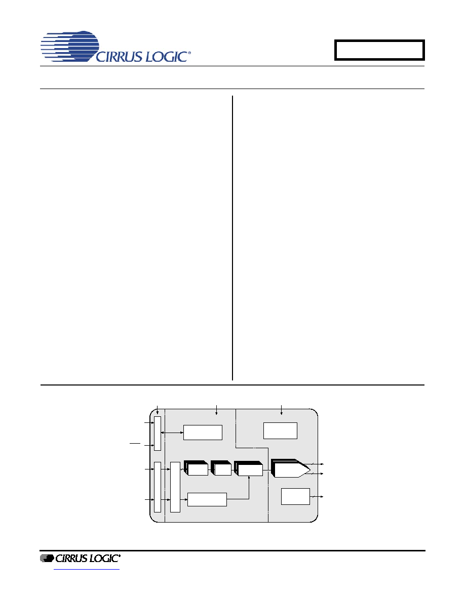
The CS4382A is a complete 8-channel digital-to-analog
system. This D/A system includes digital de-emphasis,
one-dB step size volume control, ATAPI channel mix-
ing, selectable fast and slow digital interpolation filters
followed by an oversampled, multi-bit delta sigma mod-
ulator which includes mismatch shaping technology that
eliminates distortion due to capacitor mismatch. Follow-
ing this stage is a multi-element switched capacitor
stage and low-pass filter with differential analog
outputs.
The CS4382A also has a proprietary DSD processor
which allows for 50 kHz on-chip filtering without an in-
termediate decimation stage.
The CS4382A accepts PCM data at sample rates from
4 kHz to 216 kHz, DSD audio data, and delivers excel-
lent sound quality. These features are ideal for multi-
channel audio systems including SACD players, A/V re-
ceivers, digital TV's, mixing consoles, effects
processors, sound cards and automotive audio
systems.
ORDERING INFORMATION
See page 41.
Control & Serial Audio Port
Supplies = 1.8 V to 5 V
Register/Hardware
Configuration
Internal Voltage
Reference
Reset
S
e
ri
al
In
te
r
f
ac
e
L
e
vel
Tr
an
slat
o
r
Le
vel Tra
n
sla
t
or
Digital Supply = 2.5 V
Hardware Mode or
I
2
C/SPI Software Mode
Control Data
Analog Supply = 5 V
Differential
Outputs
8
8
PCM Serial
Audio Input
Volume
Controls
Digital
Filters
Switch-Cap
DAC and
Analog Filters
Multi-bit
Modulators
DSD Audio
Input
DSD Processor
-50 kHz filter
External Mute
Control
Mute Signals
2
8
APR '05
DS618PP1
CS4382A

2
DS618PP1
CS4382A
TABLE OF CONTENTS
1. PIN DESCRIPTION..................................................................................................................... 6
2. CHARACTERISTICS AND SPECIFICATIONS.......................................................................... 8
3. APPLICATIONS ....................................................................................................................... 20
3.1 Master Clock..................................................................................................................... 20
3.2 Mode Select...................................................................................................................... 20
3.3 Digital Interface Formats .................................................................................................. 22
3.4 Oversampling Modes........................................................................................................ 23
3.5 Interpolation Filter............................................................................................................. 23
3.6 De-Emphasis .................................................................................................................... 23
3.7 ATAPI Specification.......................................................................................................... 24
3.8 Direct Stream Digital (DSD) Mode.................................................................................... 25
3.9 Grounding and Power Supply Arrangements ................................................................... 25
3.9.1 Capacitor Placement............................................................................................ 25
3.10 Analog Output and Filtering............................................................................................ 25
3.11 Mute Control ................................................................................................................... 26
3.12 Recommended Power-Up Sequence ............................................................................. 27
3.12.1 Hardware Mode ................................................................................................. 27
3.12.2 Software Mode................................................................................................... 27
3.13 Recommended Procedure for Switching Operational Modes......................................... 27
3.14 Control Port Interface ..................................................................................................... 28
3.14.1 MAP Auto Increment.......................................................................................... 28
3.14.2 I
2
C Mode............................................................................................................ 28
3.14.2.1 I
2
C Write ............................................................................................ 28
3.14.2.2 I
2
C Read ............................................................................................ 29
3.14.3 SPITM Mode........................................................................................................ 30
3.14.3.1 SPI Write............................................................................................ 30
3.15 Memory Address Pointer (MAP) ............................................................................... 30
4. REGISTER QUICK REFERENCE ............................................................................................ 31
5. REGISTER DESCRIPTION ...................................................................................................... 32
5.1 Mode Control 1 (address 01h) .......................................................................................... 32
5.1.1 Control Port Enable (CPEN) ................................................................................ 32
5.1.2 Freeze Controls (Freeze)..................................................................................... 32
5.1.3 Master Clock DIVIDE ENABLE (mclkdiv) ............................................................ 32
5.1.4 DAC Pair Disable (DACx_DIS) ............................................................................ 32
5.1.5 Power Down (PDN).............................................................................................. 33
5.2 Mode Control 2 (address 02h)......................................................................................... 33
5.2.1 Digital Interface Format (dif) ................................................................................ 33
5.2.2 Mode Control 3 (address 03h) ............................................................................ 34
5.2.3 Soft Ramp AND Zero Cross CONTROL (SZC) ................................................... 34
5.2.4 Single Volume Control (Snglvol) .......................................................................... 34
5.2.5 Soft Volume Ramp-Up after Error (RMP_UP) ..................................................... 35
5.2.6 MUTEC Polarity (MUTEC+/-)............................................................................... 35
5.2.7 Auto-Mute (AMUTE) ........................................................................................... 35
5.3 Mutec Pin Control (MUTEC) ............................................................................................. 35
5.4 Filter Control (address 04h) ............................................................................................. 36
5.4.1 Interpolation Filter Select (FILT_SEL).................................................................. 36
5.4.2 De-Emphasis Control (DEM) ............................................................................... 36
5.4.3 Soft Ramp-Down before Filter Mode Change (RMP_DN) ................................... 36
5.5 Invert Control (address 05h)............................................................................................ 37
5.5.1 Invert Signal Polarity (Inv_Xx).............................................................................. 37
5.6 Mixing Control Pair 1 (Channels A1 & B1)(address 06h)
Mixing Control Pair 2 (Channels A2 & B2)(address 09h)

DS618PP1
3
CS4382A
Mixing Control Pair 3 (Channels A3 & B3)(address 0Ch)
Mixing Control Pair 4 (Channels A4 & B4)(address 0Fh) ............................................. 37
5.6.1 Channel A Volume = Channel B Volume (A=B)................................................... 37
5.6.2 ATAPI Channel Mixing and Muting (ATAPI) ........................................................ 37
5.6.3 Functional Mode (FM).......................................................................................... 38
5.7 Volume Control (addresses 07h, 08h, 0Ah, 0Bh, 0Dh, 0Eh) .......................................... 39
5.7.1 Mute (MUTE) ....................................................................................................... 39
5.7.2 Volume Control (xx_VOL) .................................................................................... 39
5.8 Chip Revision (address 12h) ........................................................................................... 40
5.8.1 Part Number ID (part) [Read Only] ...................................................................... 40
6. PARAMETER DEFINITIONS.................................................................................................... 41
7. REFERENCES.......................................................................................................................... 41
8. ORDERING INFORMATION .................................................................................................... 41
9. PACKAGE DIMENSIONS ........................................................................................................ 42
10. APPENDIX ............................................................................................................................. 43

4
DS618PP1
CS4382A
LIST OF FIGURES
Figure 1. Serial Audio Interface Timing..................................................................................................... 14
Figure 2. Direct Stream Digital - Serial Audio Input Timing....................................................................... 15
Figure 3. Control Port Timing - I
2
C Format ............................................................................................... 16
Figure 4. Control Port Timing - SPI Format............................................................................................... 17
Figure 5. Typical Connection Diagram, Software Mode............................................................................ 18
Figure 6. Typical Connection Diagram, Hardware Mode .......................................................................... 19
Figure 7. Format 0 - Left-Justified up to 24-bit Data ................................................................................. 22
Figure 8. Format 1 - I
2
S up to 24-bit Data................................................................................................. 22
Figure 9. Format 2 - Right-Justified 16-bit Data ........................................................................................ 22
Figure 10. Format 3 - Right-Justified 24-bit Data ...................................................................................... 22
Figure 11. Format 4 - Right-Justified 20-bit Data ...................................................................................... 23
Figure 12. Format 5 - Right-Justified 18-bit Data ...................................................................................... 23
Figure 13. De-Emphasis Curve................................................................................................................. 24
Figure 14. ATAPI Block Diagram (x = channel pair 1, 2, or 3) .................................................................. 24
Figure 15. Full-Scale Output ..................................................................................................................... 26
Figure 16. Recommended Output Filter.................................................................................................... 26
Figure 17. Control Port Timing, I
2
C Mode................................................................................................. 29
Figure 18. Control Port Timing, SPI mode ................................................................................................ 30
Figure 19. Single-Speed (fast) Stopband Rejection.................................................................................. 43
Figure 20. Single-Speed (fast) Transition Band ........................................................................................ 43
Figure 21. Single-Speed (fast) Transition Band (detail) ............................................................................ 43
Figure 22. Single-Speed (fast) Passband Ripple ...................................................................................... 43
Figure 23. Single-Speed (slow) Stopband Rejection ................................................................................ 43
Figure 24. Single-Speed (slow) Transition Band....................................................................................... 43
Figure 25. Single-Speed (slow) Transition Band (detail)........................................................................... 44
Figure 26. Single-Speed (slow) Passband Ripple..................................................................................... 44
Figure 27. Double-Speed (fast) Stopband Rejection ................................................................................ 44
Figure 28. Double-Speed (fast) Transition Band....................................................................................... 44
Figure 29. Double-Speed (fast) Transition Band (detail)........................................................................... 44
Figure 30. Double-Speed (fast) Passband Ripple..................................................................................... 44
Figure 31. Double-Speed (slow) Stopband Rejection ............................................................................... 45
Figure 32. Double-Speed (slow) Transition Band ..................................................................................... 45
Figure 33. Double-Speed (slow) Transition Band (detail) ......................................................................... 45
Figure 34. Double-Speed (slow) Passband Ripple ................................................................................... 45
Figure 35. Quad-Speed (fast) Stopband Rejection ................................................................................... 45
Figure 36. Quad-Speed (fast) Transition Band ......................................................................................... 45
Figure 37. Quad-Speed (fast) Transition Band (detail) ............................................................................. 46
Figure 38. Quad-Speed (fast) Passband Ripple ....................................................................................... 46
Figure 39. Quad-Speed (slow) Stopband Rejection.................................................................................. 46
Figure 40. Quad-Speed (slow) Transition Band........................................................................................ 46
Figure 41. Quad-Speed (slow) Transition Band (detail)............................................................................ 46
Figure 42. Quad-Speed (slow) Passband Ripple...................................................................................... 46
