 | –≠–ª–µ–∫—Ç—Ä–æ–Ω–Ω—ã–π –∫–æ–º–ø–æ–Ω–µ–Ω—Ç: CS4398 | –°–∫–∞—á–∞—Ç—å:  PDF PDF  ZIP ZIP |
Copyright
© Cirrus Logic, Inc. 2005
(All Rights Reserved)
http://www.cirrus.com
120 dB, 192 kHz Multi-Bit DAC with Volume Control
Features
Advanced Multi-bit Delta-Sigma Architecture
≠ 120 dB Dynamic Range
≠ -107 dB THD+N
≠ Low Clock Jitter Sensitivity
≠ Differential Analog Outputs
PCM input
≠ 102 dB of Stopband Attenuation
≠ Supports Sample Rates up to 192 kHz
≠ Accepts up to 24 bit Audio Data
≠ Supports All Industry Standard Audio
Interface Formats
≠ Selectable Digital Filter Response
≠ Volume Control with 1/2 dB Step Size and
Soft Ramp
≠ Flexible Channel Routing and Mixing
≠ Selectable De-Emphasis
Supports Stand-Alone or I≤C/SPI
TM
Configuration
Embedded Level Translators
≠ 1.8 V to 5 V Serial Audio Input
≠ 1.8 V to 5 V Control Data Input
Direct Stream Digital (DSD)
≠ Dedicated DSD Input Pins
≠ On-Chip 50 kHz Filter to Meet Scarlet Book
SACD Recommendations
≠ Matched PCM and DSD Analog Output
Levels
≠ Non-Decimating Volume Control with
1/2 dB Step Size and Soft Ramp
≠ DSD Mute Detection
≠ Supports Phase-Modulated Inputs
≠ Optional Direct DSD Path to On-Chip
Switched Capacitor Filter
Control Output for External Muting
≠ Independent Left and Right Mute Controls
≠ Supports Auto Detection of Mute Output
Polarity
Typical Applications
≠ DVD Players
≠ SACD Players
≠ A/V Receivers
≠ Professional Audio Products
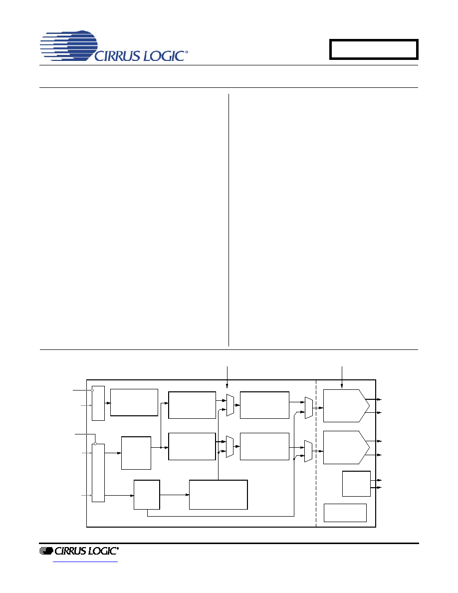
PCM
Serial
Interface
Multibit
Modulator
Interpolation
Filter with
Volume Control
Internal Voltage
Reference
External
Mute
Control
Switched
Capacitor
DAC and
Filter
DSD
Interface
PCM Input
Left and Right
Mute Controls
Right
Differential
Output
Left
Differential
Output
DSD Input
DSD Processor
1.8 V to 5V
1.8 V to 5 V
-Volume control
-50kHz filter
Switched
Capacitor
DAC and
Filter
MU
X
Direct DSD
Lev
el
T
r
ans
l
at
or
Le
v
e
l
Tr
a
n
s
l
a
t
o
r
Hardware or I
2
C/SPI
Control Data
MUX
Multibit
Modulator
Interpolation
Filter with
Volume Control
MUX
MUX
3.3 V to 5 V
5 V
Register/Hardware
Configuration
JULY '05
DS568F1
CS4398

2
DS568F1
CS4398
Stand-Alone Mode Features
Selectable Oversampling Modes
≠ 32 kHz to 54 kHz Sampling Rates
≠ 50 kHz to 108 kHz Sampling Rates
≠ 100 kHz to 216 kHz Sampling Rates
Selectable Serial Audio Interface Formats
≠ Left-Justified, up to 24 bit
≠ I≤S, up to 24 bit
≠ Right-Justified 16 bit
≠ Right-Justified 24 bit
Auto Mute Output Polarity Detect
Auto Mute on Static PCM Samples
44.1 kHz 50/15
µs De-Emphasis Available
Soft Volume Ramp-up after Reset is Released
Control Port Mode Features
Selectable Oversampling Modes
≠ 32 kHz to 54 kHz Sampling Rates
≠ 50 kHz to 108 kHz Sampling Rates
≠ 100 kHz to 216 kHz Sampling Rates
Selectable Serial Audio Interface Formats
≠ Left-Justified, up to 24 bit
≠ I≤S, up to 24 bit
≠ Right-Justified 16 bit
≠ Right-Justified 18 bit
≠ Right-Justified 20 bit
≠ Right-Justified 24 bit
Direct Stream Digital Mode
Selectable Auto or Manual Mute Polarity
Selectable Interpolation Filters
Selectable 32, 44.1, and 48 kHz De-Emphasis
Configurable ATAPI Mixing Functions
Configurable Volume and Muting Controls
Description
The CS4398 is a complete stereo 24 bit/192 kHz digital-
to-analog system. This D/A system includes digital de-
emphasis, half dB step size volume control, ATAPI
channel mixing, selectable fast and slow digital interpo-
lation filters followed by an oversampled multi-bit delta-
sigma modulator that includes mismatch shaping tech-
nology that eliminates distortion due to capacitor
mismatch. Following this stage is a multi-element
switched capacitor stage and low pass filter with differ-
ential analog outputs.
The CS4398 also has an proprietary DSD processor
that allows for volume control and 50 kHz on-chip filter-
ing without an intermediate decimation stage. It also
offers an optional path for direct DSD conversion by di-
rectly using the multi-element switched capacitor array.
The CS4398 accepts PCM data at sample rates from
32 kHz to 216 kHz, DSD audio data, has selectable dig-
ital filters, consumes little power, and delivers excellent
sound quality.
ORDERING INFORMATION
Product
Description
Package
Pb-Free
Grade
Temp Range
Container
Order #
CS4398
120 dB, 192 kHz Multi-
Bit DAC with Volume
Control
28-pin
TSSOP
YES
Commercial -10∞ to +70∞ C
Rail
CS4398-CZZ
Tape & Reel
CS4398-CZZR
CDB4398
CS4398 Evaluation Board
-
-
-
-
CDB4398

DS568F1
3
CS4398
TABLE OF CONTENTS
1. PINOUT DRAWING ................................................................................................................. 6
2. CHARACTERISTICS AND SPECIFICATIONS ........................................................................ 8
SPECIFIED OPERATING CONDITIONS ................................................................................. 8
ABSOLUTE MAXIMUM RATINGS ........................................................................................... 8
ANALOG CHARACTERISTICS................................................................................................ 9
COMBINED INTERPOLATION & ON-CHIP ANALOG FILTER RESPONSE ........................ 10
COMBINED INTERPOLATION & ON-CHIP ANALOG FILTER RESPONSE ........................ 11
DSD COMBINED DIGITAL AND ON-CHIP ANALOG FILTER RESPONSE.......................... 11
SWITCHING CHARACTERISTICS ........................................................................................ 12
SWITCHING CHARACTERISTICS - DSD ............................................................................. 14
SWITCHING CHARACTERISTICS - CONTROL PORT - I≤C FORMAT ................................ 15
SWITCHING CHARACTERISTICS - CONTROL PORT - SPITM FORMAT............................ 16
DC ELECTRICAL CHARACTERISTICS ............................................................................... 17
DIGITAL INTERFACE SPECIFICATIONS ............................................................................. 18
3. TYPICAL CONNECTION DIAGRAM .................................................................................. 19
4. APPLICATIONS ..................................................................................................................... 20
4.1 Grounding and Power Supply Decoupling ....................................................................... 20
4.2 Analog Output and Filtering ............................................................................................. 20
4.3 The MUTEC Outputs ....................................................................................................... 20
4.4 Oversampling Modes ....................................................................................................... 21
4.5 Master and Serial Clock Ratios ....................................................................................... 21
4.6 Stand-Alone Mode Settings ............................................................................................. 22
4.7 Control Port Mode ........................................................................................................... 23
5. CONTROL PORT INTERFACE ............................................................................................. 25
5.1 Memory Address Pointer (MAP) ...................................................................................... 25
5.2 Enabling the Control Port ................................................................................................ 25
5.3 Format Selection ............................................................................................................. 25
5.4 I≤C Format ....................................................................................................................... 25
5.5 SPI Format ...................................................................................................................... 26
7.1 Chip ID - Register 01h ..................................................................................................... 29
7.2 Mode Control 1 - Register 02h ........................................................................................ 29
7.3 Volume Mixing and Inversion Control - Register 03h ...................................................... 30
7.4 Mute Control - Register 04h ............................................................................................ 33
7.5 Channel A Volume Control - Register 05h ....................................................................... 34
7.6 Channel B Volume Control - Register 06h ....................................................................... 34
7.7 Ramp and Filter Control - Register 07h ........................................................................... 35
7.8 Misc. Control - Register 08h ............................................................................................ 37
7.9 Misc. Control - Register 09h ............................................................................................ 38
8. PARAMETER DEFINITIONS .................................................................................................. 39
9. REFERENCES ........................................................................................................................ 39
10. PACKAGE DIMENSIONS .................................................................................................... 40
10.1 28-TSSOP ..................................................................................................................... 40
THERMAL CHARACTERISTICS AND SPECIFICATIONS ................................................... 40
11. APPENDIX ....................................................................................................................... 41

4
DS568F1
CS4398
LIST OF FIGURES
Figure 1. Pinout Drawing................................................................................................................. 6
Figure 2. Serial Mode Input Timing ............................................................................................... 12
Figure 3. Format 0 - Left-Justified up to 24-bit Data ..................................................................... 13
Figure 4. Format 1 - I≤S up to 24-bit Data ..................................................................................... 13
Figure 5. Format 2, Right-Justified 16-Bit Data.
Format 3, Right-Justified 24-Bit Data.
Format 4, Right-Justified 20-Bit Data. (Available in Control Port Mode only)
Format 5, Right-Justified 18-Bit Data. (Available in Control Port Mode only) ................ 13
Figure 6. Direct Stream Digital - Serial Audio Input Timing........................................................... 14
Figure 7. Direct Stream Digital - Serial Audio Input Timing for Phase Modulation Mode.............. 14
Figure 8. Control Port Timing - I≤C Format.................................................................................... 15
Figure 9. Control Port Timing - SPI Format (Read/Write) ............................................................. 16
Figure 10. Typical Connection Diagram........................................................................................ 19
Figure 11. Recommended Output Filter........................................................................................ 20
Figure 12. Recommended Mute Circuitry ..................................................................................... 21
Figure 13. DSD Phase Modulation Mode Diagram ....................................................................... 24
Figure 14. Control Port Timing, I≤C Format................................................................................... 26
Figure 15. Control Port Timing, SPI Format (Write) ...................................................................... 27
Figure 16. Control Port Timing, SPI Format (Read)...................................................................... 27
Figure 17. De-Emphasis Curve..................................................................................................... 30
Figure 18. ATAPI Block Diagram .................................................................................................. 31
Figure 19. 28L TSSOP (4.4 mm Body) Package Drawing ............................................................ 40
Figure 20. Single-Speed (fast) Stopband Rejection...................................................................... 41
Figure 21. Single-Speed (fast) Transition Band ............................................................................ 41
Figure 22. Single-Speed (fast) Transition Band (detail) ................................................................ 41
Figure 23. Single-Speed (fast) Passband Ripple .......................................................................... 41
Figure 24. Single-Speed (slow) Stopband Rejection .................................................................... 41
Figure 25. Single-Speed (slow) Transition Band........................................................................... 41
Figure 26. Single-Speed (slow) Transition Band (detail)............................................................... 42
Figure 27. Single-Speed (slow) Passband Ripple......................................................................... 42
Figure 28. Double-Speed (fast) Stopband Rejection .................................................................... 42
Figure 29. Double-Speed (fast) Transition Band........................................................................... 42
Figure 30. Double-Speed (fast) Transition Band (detail)............................................................... 42
Figure 31. Double-Speed (fast) Passband Ripple......................................................................... 42
Figure 32. Double-Speed (slow) Stopband Rejection ................................................................... 43
Figure 33. Double-Speed (slow) Transition Band ......................................................................... 43
Figure 34. Double-Speed (slow) Transition Band (detail) ............................................................. 43
Figure 35. Double-Speed (slow) Passband Ripple ....................................................................... 43
Figure 36. Quad-Speed (fast) Stopband Rejection ....................................................................... 43
Figure 37. Quad-Speed (fast) Transition Band ............................................................................. 43
Figure 38. Quad-Speed (fast) Transition Band (detail) ................................................................. 44
Figure 39. Quad-Speed (fast) Passband Ripple ........................................................................... 44
Figure 40. Quad-Speed (slow) Stopband Rejection...................................................................... 44
Figure 41. Quad-Speed (slow) Transition Band............................................................................ 44
Figure 42. Quad-Speed (slow) Transition Band (detail)................................................................ 44
Figure 43. Quad-Speed (slow) Passband Ripple.......................................................................... 44

DS568F1
5
CS4398
LIST OF TABLES
Table 1. Clock Ratios .................................................................................................................... 21
Table 2. Common Clock Frequencies........................................................................................... 22
Table 3. Digital Interface Format, Stand-Alone Mode Options...................................................... 22
Table 4. Mode Selection, Stand-Alone Mode Options .................................................................. 22
Table 5. Digital Interface Formats - PCM Mode............................................................................ 29
Table 6. Digital Interface Formats - DSD Mode ............................................................................ 30
Table 7. Example Digital Volume Settings .................................................................................... 34
Table 8. Revision Table ................................................................................................................ 45
6
DS568F1
CS4398
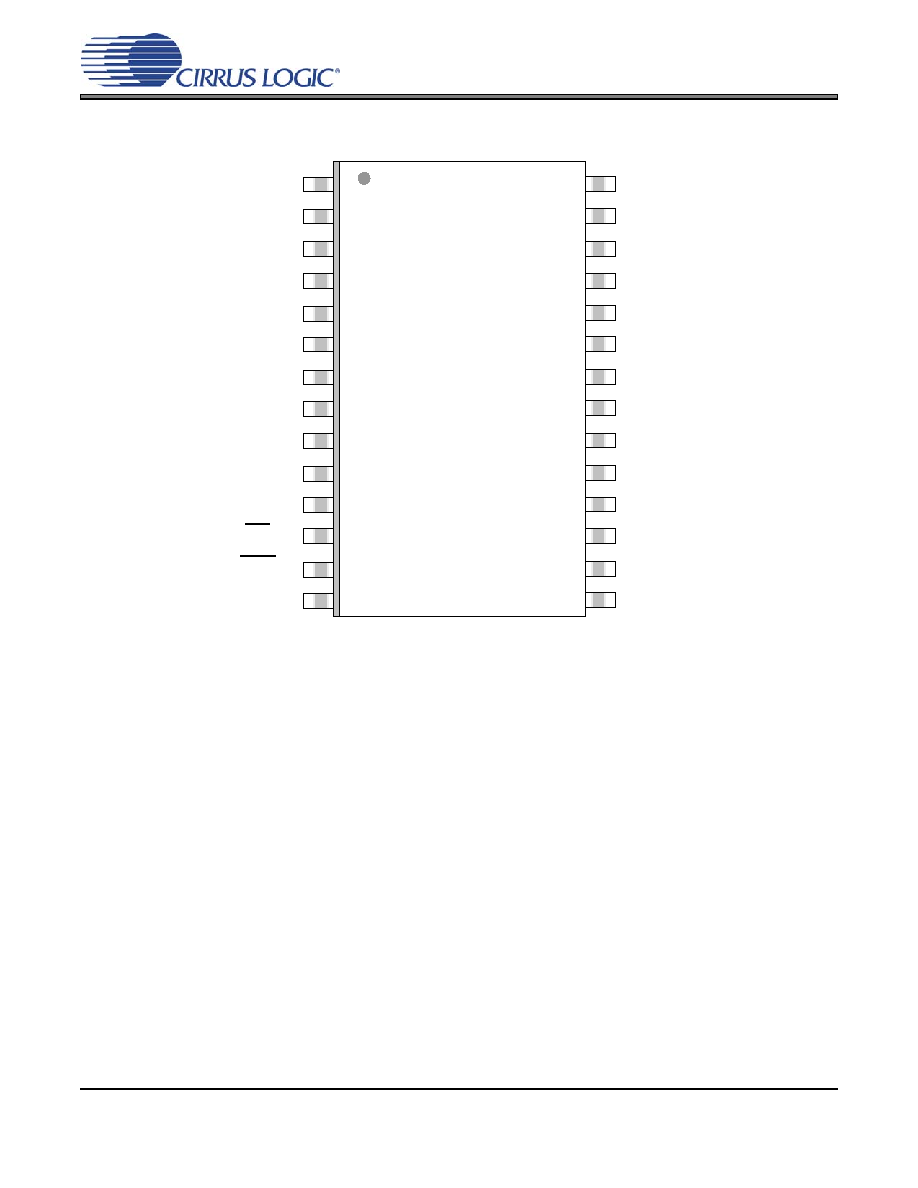
1. PINOUT DRAWING
Figure 1. Pinout Drawing
DSD_B
DSD_A
DSD_SCLK
VLS
SDIN
VQ
SCLK
AMUTEC
LRCK
AOUTA-
MCLK
AOUTA+
VD
VA
DGND
AGND
M3 (AD1/CDIN)
AOUTB+
M2 (SCL/CCLK)
AOUTB-
M1 (SDA/CDOUT)
BMUTEC
M0 (AD0/CS)
VREF
RST
REF_GND
VLC
FILT+
1
2
3
4
5
6
7
8
21
22
23
24
25
26
27
28
9
10
11
12
17
18
19
20
13
14
15
16

DS568F1
7
CS4398
Pin Name
Pin #
Pin Description
DSD_A
DSD_B
28
1
Direct Stream Digital Input (Input) - Input for Direct Stream Digital serial audio data.
DSD_SCLK
2
DSD Serial Clock (Input) - Serial clock for the Direct Stream Digital audio interface.
SDIN
3
Serial Audio Data Input (Input) - Input for two's complement serial audio data.
SCLK
4
Serial Clock (Input) - Serial clock for the serial audio interface.
LRCK
5
Left Right Clock (Input) - Determines which channel, Left or Right, is currently active on
the serial audio data line.
MCLK
6
Master Clock (Input) - Clock source for the delta-sigma modulator and digital filters.
VD
7
Digital Power (Input) - Positive power for the digital section.
DGND
8
Digital Ground (Input) - Ground reference for the digital section.
RST
13
Reset (Input) - The device enters system reset when enabled.
VLC
14
Control Port Power (Input) - Positive power for Control Port I/O.
FILT+
15
Positive Voltage Reference (Output) - Positive reference voltage for the internal sam-
pling circuits.
REF_GND
16
Reference Ground (Input) - Ground reference for the internal sampling circuits.
VREF
17
Voltage Reference (Input) - Positive voltage reference for the internal sampling circuits.
BMUTEC
AMUTEC
18
25
Mute Control (Output) - The Mute Control pin is active during power-up initialization, mut-
ing, power-down or if the master clock to left/right clock frequency ratio is incorrect. During
reset, these outputs are set to a high impedance.
AOUTB+
AOUTB-
20
19
Differential Right Channel Analog Output (Output) - The full-scale differential analog
output level is specified in the Analog Characteristics specification table.
AGND
21
Analog Ground (Input) - Ground reference for the analog section.
VA
22
Analog Power (Input) - Positive power for the analog section.
AOUTA+
AOUTA-
23
24
Differential Left Channel Analog Output (Output) - The full-scale differential analog out-
put level is specified in the Analog Characteristics specification table.
VQ
26
Quiescent Voltage (Output) - Filter connection for internal quiescent voltage.
VLS
27
Serial Audio Interface Power (Input) - Positive power for serial audio interface I/O.
Stand-Alone Mode Definitions
M3
M2
M1
M0
9
10
11
12
Mode Selection (Input) - Determines the operational mode of the device.
Control Port Mode Definitions
AD1/CDIN
9
Address Bit 1 (I≤C) / Control Data Input (SPI) (Input) - AD1 is a chip address pin in I≤C
mode; CDIN is the input data line for the Control Port interface in SPI mode.
SCL/CCLK
10
Serial Control Port Clock (Input) - Serial clock for the serial Control Port.
SDA/CDOUT
11
Serial Control Data (I≤C) / Control Data Output (SPI) (Input/Output) - SDA is a data I/O
line in I≤C mode. CDOUT is the output data line for the Control Port interface in SPI mode.
AD0/CS
12
Address Bit 0 (I≤C) / Control Port Chip Select (SPI) (Input) - AD0 is a chip address pin
in I≤C mode; CS is the chip select signal for SPI format.
8
DS568F1
CS4398
2. CHARACTERISTICS AND SPECIFICATIONS
(Min/Max performance characteristics and specifications are guaranteed over the Specified Operating Conditions.
Typical performance characteristics are derived from measurements taken at T
A
= 25
∞C, VA = 5.0 V, VD = 3.3 V.)
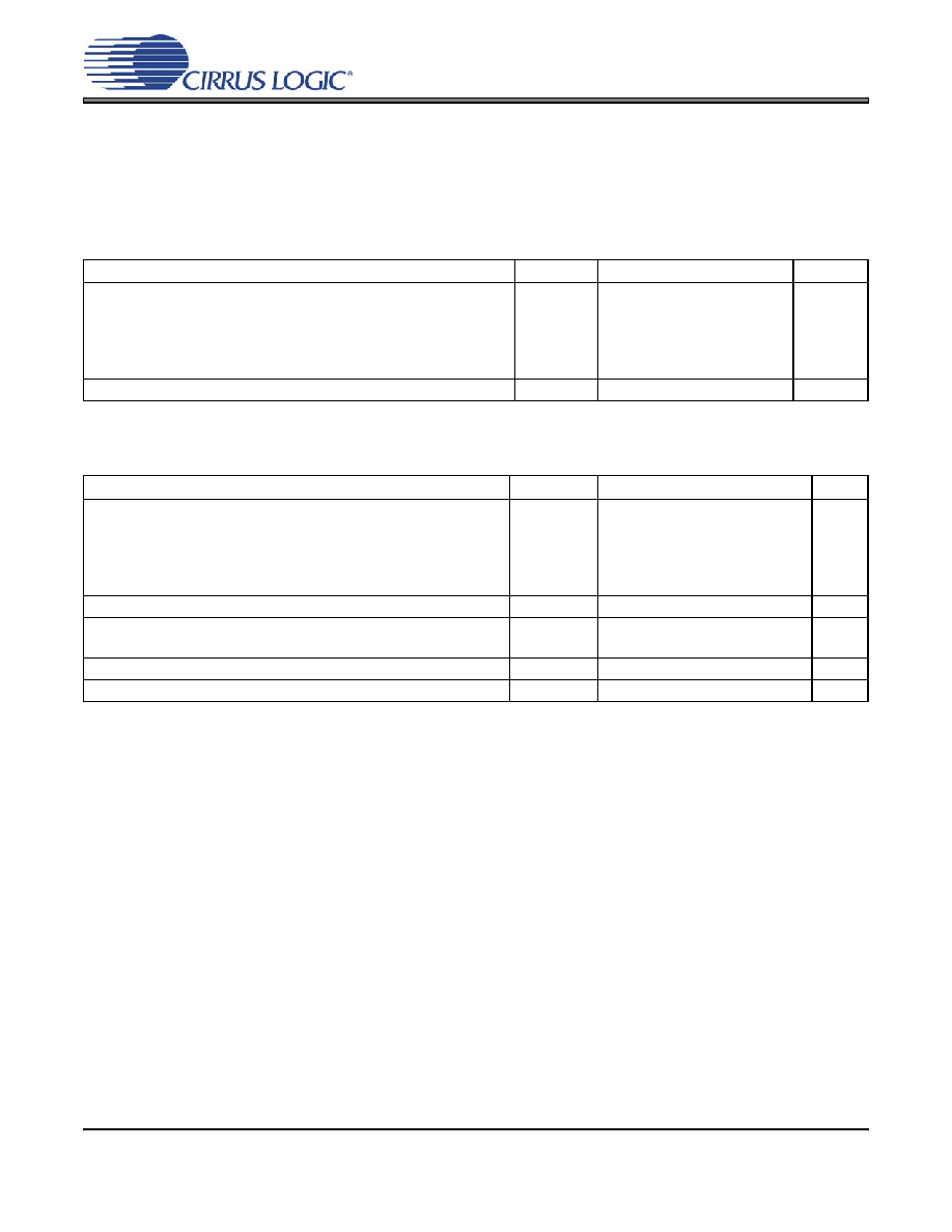
SPECIFIED OPERATING CONDITIONS
(AGND = 0 V; all voltages with respect to ground.)
ABSOLUTE MAXIMUM RATINGS
(AGND = 0 V; all voltages with respect to ground.)
WARNING: Operation at or beyond these limits may result in permanent damage to the device. Normal operation
is not guaranteed at these extremes.
Parameters
Symbol Min Typ
Max
Units
DC Power Supply
Analog power
Voltage reference
Digital power
Serial audio interface power
Control port interface power
VA
VREF
VD
VLS
VLC
4.75
4.75
3.1
1.7
1.7
5.0
5.0
3.3
3.3
3.3
5.25
5.25
5.25
5.25
5.25
V
V
V
V
V
Specified Temperature Range
-CZ & -CZZ
T
A
-10
-
70
∞C
Parameters
Symbol
Min
Max
Units
DC Power Supply
Analog power
Voltage reference
Digital power
Serial audio interface power
Control port interface power
VA
VREF
VD
VLS
VLC
-0.3
-0.3
-0.3
-0.3
-0.3
6.0
6.0
6.0
6.0
6.0
V
V
V
V
V
Input Current
any pin except supplies
I
in
-
±10
mA
Digital Input Voltage
Serial audio interface
Control port interface
V
IN-LS
V
IN-LC
-0.3
-0.3
VLS+ 0.4
VLC+ 0.4
V
V
Ambient Operating Temperature (power applied)
T
A
-55
125
∞C
Storage Temperature
T
stg
-65
150
∞C
DS568F1
9
CS4398
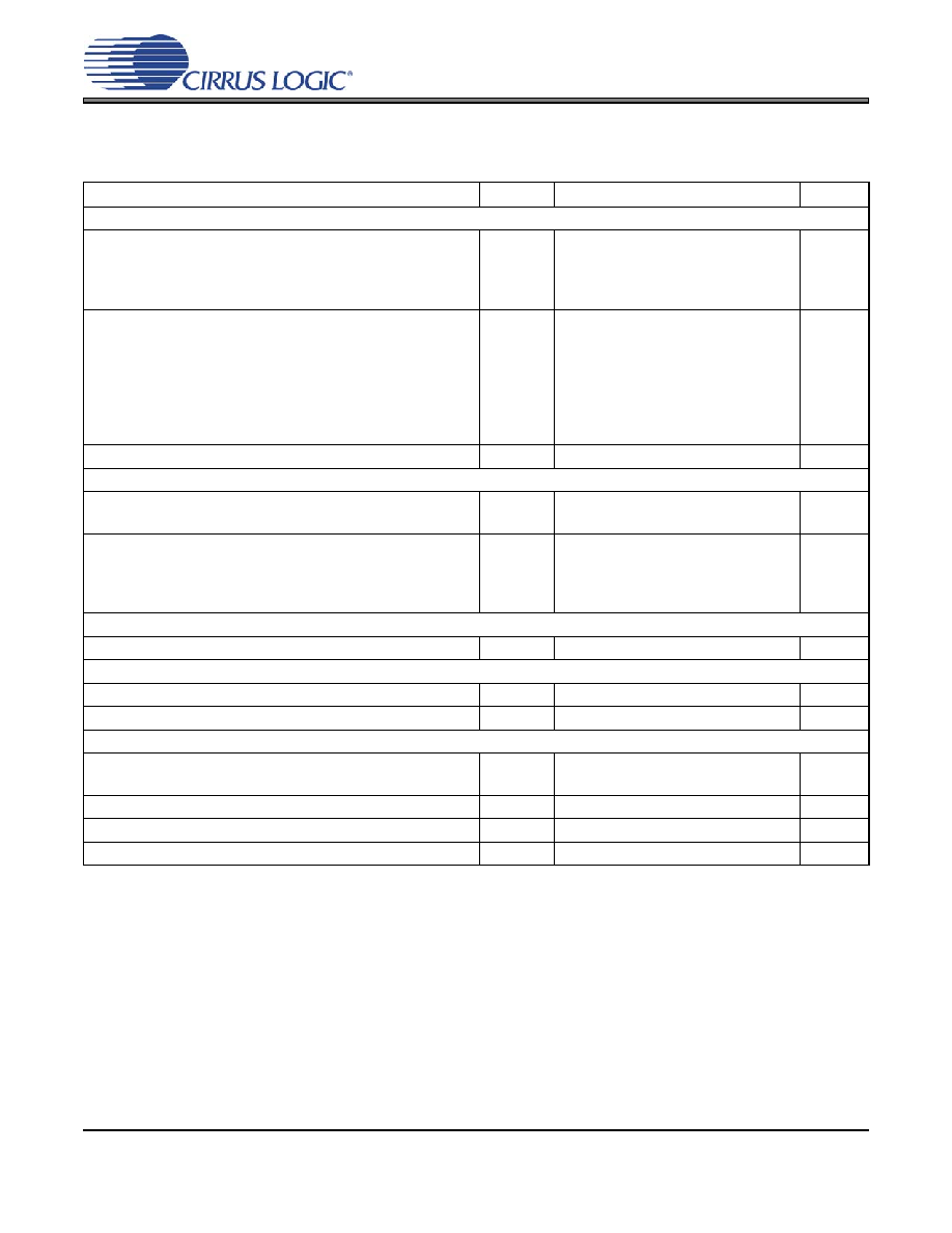
ANALOG CHARACTERISTICS
(Test conditions (unless otherwise specified): Input test signal is a 997 Hz sine wave at 0 dBFS; measurement
bandwidth is 10 Hz to 20 kHz; test load R
L
= 1 k
, C
L
= 10 pF.)
Notes:
1. One-half LSB of triangular PDF dither is added to data.
2. Performance limited by 16-bit quantization noise.
3. DSD performance may be limited by the source recording. 0 dB-SACD = 50% modulation index.
Parameter
Symbol
Min
Typ
Max
Unit
Dynamic Performance - All PCM modes and DSD Processor mode
Dynamic Range (Note 1)
24-bit A-Weighted
unweighted
16-bit A-Weighted
(Note 2) unweighted
114
111
-
-
120
117
97
94
-
-
-
-
dB
dB
dB
dB
Total Harmonic Distortion + Noise
(Note 1)
24-bit 0 dB
-20 dB
-60 dB
16-bit 0 dB
(Note 2) -20 dB
-60 dB
THD+N
-
-
-
-
-
-
-107
-97
-57
-94
-74
-34
-100
-
-
-
-
-
dB
dB
dB
dB
dB
dB
Idle Channel Noise / Signal-to-noise ratio
-
120
-
dB
Dynamic Performance - Direct DSD
Dynamic Range (Note 3)
A-Weighted
unweighted
111
108
117
114
-
-
dB
dB
Total Harmonic Distortion + Noise
(Note 3)
0 dB
-20 dB
-60 dB
THD+N
-
-
-
-104
-94
-54
-98
-
-
dB
dB
dB
Dynamic Performance for All Modes
Interchannel Isolation
(1 kHz)
-
110
-
dB
DC Accuracy
Interchannel Gain Mismatch
ICGM
-
0.1
-
dB
Gain Drift
-
100
-
ppm/∞C
Analog Output Characteristics and Specifications
Full Scale Differential
PCM, DSD processor
Output Voltage
Direct DSD mode
132%∑V
A
94%∑V
A
134%∑V
A
96%∑V
A
136%∑V
A
98%∑V
A
Vpp
Vpp
Output Impedance
Z
OUT
-
118
-
Minimum AC-Load Resistance
R
L
-
1
-
k
Maximum Load Capacitance
C
L
-
100
-
pF
10
DS568F1
CS4398
COMBINED INTERPOLATION & ON-CHIP ANALOG FILTER RESPONSE
The filter characteristics have been normalized to the sample rate (Fs) and can be referenced to the desired sam-
ple rate by multiplying the given characteristic by Fs.)
(See note 9.)
4. Slow Roll-off interpolation filter is only available in Control Port mode.
5. Filter response is guaranteed by design.
6. Response is clock-dependent and will scale with Fs.
7. For Single-Speed Mode, the Measurement Bandwidth is from stopband to 3 Fs.
For Double-Speed Mode, the Measurement Bandwidth is from stopband to 3 Fs.
For Quad-Speed Mode, the Measurement Bandwidth is from stopband to 1.34 Fs.
8. De-emphasis is available only in Single-Speed Mode; Only 44.1 kHz De-emphasis is available in Stand-
Alone mode.
9. Amplitude vs. Frequency plots of this data are available in the "Appendix" on page 41.
Parameter
Fast Roll-Off
Unit
Min Typ
Max
Combined Digital and On-Chip Analog Filter Response - Single-Speed Mode - 48 kHz (Note 5)
Passband (Note 6)
to -0.01 dB corner
to -3 dB corner
0
0
-
-
.454
.499
Fs
Fs
Frequency Response 10 Hz to 20 kHz
-0.01
-
+0.01
dB
StopBand
0.547
-
-
Fs
StopBand Attenuation
(Note 7)
102
-
-
dB
Group Delay
-
9.4/Fs
-
s
De-emphasis Error (Note 8)
Fs = 32 kHz
(Relative to 1 kHz)
Fs = 44.1 kHz
Fs = 48 kHz
-
-
-
-
-
-
±0.23
±0.14
±0.09
dB
dB
dB
Combined Digital and On-Chip Analog Filter Response - Double-Speed Mode - 96 kHz (Note 5)
Passband (Note 6)
to -0.01 dB corner
to -3 dB corner
0
0
-
-
.430
.499
Fs
Fs
Frequency Response 10 Hz to 20 kHz
-0.01
-
0.01
dB
StopBand
.583
-
-
Fs
StopBand Attenuation
(Note 7)
80
-
-
dB
Group Delay
-
4.6/Fs
-
s
Combined Digital and On-Chip Analog Filter Response - Quad-Speed Mode - 192 kHz (Note 5)
Passband (Note 6)
to -0.01 dB corner
to -3 dB corner
0
0
-
-
.105
.490
Fs
Fs
Frequency Response 10 Hz to 20 kHz
-0.01
-
0.01
dB
StopBand
.635
-
-
Fs
StopBand Attenuation
(Note 7)
90
-
-
dB
Group Delay
-
4.7/Fs
-
s

DS568F1
11
CS4398
COMBINED INTERPOLATION & ON-CHIP ANALOG FILTER RESPONSE
(Continued)
DSD COMBINED DIGITAL AND ON-CHIP ANALOG FILTER RESPONSE
Parameter
Slow Roll-Off (Note 4)
Unit
Min
Typ
Max
Single-Speed Mode - 48 kHz (Note 5)
Passband (Note 6)
to -0.01 dB corner
to -3 dB corner
0
0
-
-
0.417
0.499
Fs
Fs
Frequency Response 10 Hz to 20 kHz
-0.01
-
+0.01
dB
StopBand
.583
-
-
Fs
StopBand Attenuation
(Note 7)
64
-
-
dB
Group Delay
-
6.65/Fs
-
s
De-emphasis Error (Note 8)
Fs = 32 kHz
(Relative to 1 kHz)
Fs = 44.1 kHz
Fs = 48 kHz
-
-
-
-
-
-
±0.23
±0.14
±0.09
dB
dB
dB
Double-Speed Mode - 96 kHz (Note 5)
Passband (Note 6)
to -0.01 dB corner
to -3 dB corner
0
0
-
-
.296
.499
Fs
Fs
Frequency Response 10 Hz to 20 kHz
-0.01
-
0.01
dB
StopBand
.792
-
-
Fs
StopBand Attenuation
(Note 7)
70
-
-
dB
Group Delay
-
3.9/Fs
-
s
Quad-Speed Mode - 192 kHz (Note 5)
Passband (Note 6)
to -0.01 dB corner
to -3 dB corner
0
0
-
-
.104
.481
Fs
Fs
Frequency Response 10 Hz to 20 kHz
-0.01
-
0.01
dB
StopBand
.868
-
-
Fs
StopBand Attenuation
(Note 7)
75
-
-
dB
Group Delay
-
4.2/Fs
-
s
Parameter
Min
Typ
Max
Unit
DSD Processor Mode (Note 5)
Passband (Note 6)
to -3 dB corner
0
-
50
kHz
Frequency Response 10 Hz to 20 kHz
-0.05
-
0.05
dB
Roll-off
27
-
-
dB/Oct
Direct DSD Mode (Note 5)
Passband (Note 6)
to -0.1 dB corner
to -3 dB corner
0
0
-
-
26.9
176.4
kHz
kHz
Frequency Response 10 Hz to 20 kHz
-0.1
-
0
dB

12
DS568F1
CS4398
SWITCHING CHARACTERISTICS
(Inputs: Logic 0 = GND, Logic 1 = VLS, CL = 20 pF)
Parameters
Symbol Min Typ
Max
Units
Input Sample Rate
Single-Speed Mode
Double-Speed Mode
Quad-Speed Mode
Fs
Fs
Fs
30
50
100
-
-
-
54
108
216
kHz
kHz
kHz
MCLK Frequency
See Tables 1 & 2 (page 21) for compatible frequencies
MCLK Duty Cycle
40%
-
60%
LRCK Duty Cycle
45%
50
55%
SCLK Pulse Width Low
t
sclkl
20
-
-
ns
SCLK Pulse Width High
t
sclkh
20
-
-
ns
SCLK Period
Single-Speed Mode
t
sclkw
-
-
ns
Double-Speed Mode
t
sclkw
-
-
ns
Quad-Speed Mode
t
sclkw
-
-
ns
SCLK rising to LRCK edge delay
t
slrd
20
-
-
ns
SCLK rising to LRCK edge setup time
t
slrs
20
-
-
ns
SDATA valid to SCLK rising setup time
t
sdlrs
22
-
-
ns
SCLK rising to SDATA hold time
t
sdh
20
-
-
ns
sclkh
t
slrs
t
slrd
t
sdlrs
t
sd h
t
sclkl
t
S D A TA
S C LK
LR C K
Figure 2. Serial Mode Input Timing
1
128
(
)Fs
---------------------
1
64
( )Fs
------------------
2
MCLK
-----------------
DS568F1
13
CS4398
L R C K
S C L K
L e ft C h a n n e l
R ig h t C h a n n e l
S D A T A
+3 +2 +1 LS B
+5 +4
M SB -1 -2 -3 -4 -5
+3 +2 +1 LS B
+5 +4
M SB -1 -2 -3 -4
Figure 3. Format 0 - Left-Justified up to 24-bit Data
L R C K
S C L K
L e ft C h a n n e l
R ig h t C h a n n e l
S D A T A
+3 +2 +1 LSB
+5 +4
MSB -1 -2 -3 -4 -5
+3 +2 +1 LSB
+5 +4
M SB -1 -2 -3 -4
Figure 4. Format 1 - I≤S up to 24-bit Data
LR C K
S C LK
L e ft C h a n ne l
S D A TA
+5 +4 +3 +2 +1 LSB
MSB-1 -2 -3 -4 -5
3 2 c lo ck s
R ig h t C h a n n e l
LSB
+5 +4 +3 +2 +1 LSB
MSB -1 -2 -3 -4 -5
+6
-6
+6
-6
Figure 5. Format 2, Right-Justified 16-Bit Data.
Format 3, Right-Justified 24-Bit Data.
Format 4, Right-Justified 20-Bit Data. (Available in Control Port Mode only)
Format 5, Right-Justified 18-Bit Data. (Available in Control Port Mode only)

14
DS568F1
CS4398
SWITCHING CHARACTERISTICS - DSD
(Logic 0 = AGND = DGND; Logic 1 = VLS Volts; C
L
= 20 pF)
Parameter
Symbol Min Typ
Max
Unit
MCLK Duty Cycle
40
-
60
%
DSD_SCLK Pulse Width Low
t
sclkl
160
-
-
ns
DSD_SCLK Pulse Width High
t
sclkh
160
-
-
ns
DSD_SCLK Frequency
(64x Oversampled)
(128x Oversampled)
1.024
2.048
-
-
3.2
6.4
MHz
MHz
DSD_A / _B valid to DSD_SCLK rising setup time
t
sdlrs
20
-
-
ns
DSD_SCLK rising to DSD_A or DSD_B hold time
t
sdh
20
-
-
ns
DSD clock to data transition (Phase Modulation mode)
t
dpm
-20
-
20
ns
sclkh
t
sclkl
t
DSD_A,DSD_B
D SD _S C LK
sdlrs
t
sdh
t
Figure 6. Direct Stream Digital - Serial Audio Input Timing
d p m
t
DSD_A, DSD_B
D S D _ S C L K
( 6 4 F s )
D S D _ S C L K
( 1 2 8 F s )
d p m
t
Figure 7. Direct Stream Digital - Serial Audio Input Timing for Phase Modulation Mode
DS568F1
15
CS4398
SWITCHING CHARACTERISTICS - CONTROL PORT - I≤C FORMAT
(Inputs: Logic 0 = GND, Logic 1 = VLC, C
L
= 20 pF)
10. Data must be held for sufficient time to bridge the transition time, t
fc
, of SCL.
Parameter
Symbol
Min
Max
Unit
SCL Clock Frequency
f
scl
-
100
kHz
RST Rising Edge to Start
t
irs
500
-
ns
Bus Free-Time Between Transmissions
t
buf
4.7
-
µs
Start Condition Hold Time (prior to first clock pulse)
t
hdst
4.0
-
µs
Clock Low Time
t
low
4.7
-
µs
Clock High Time
t
high
4.0
-
µs
Setup Time for Repeated Start Condition
t
sust
4.7
-
µs
SDA Hold Time from SCL Falling
(Note 10)
t
hdd
0
-
µs
SDA Setup Time to SCL Rising
t
sud
250
-
ns
Rise Time of SCL and SDA
t
rc
, t
rd
-
1
µs
Fall Time SCL and SDA
t
fc
, t
fd
-
300
ns
Setup Time for Stop Condition
t
susp
4.7
-
µs
Acknowledge Delay from SCL Falling
t
ack
300
1000
ns
t buf
t
hd st
t
l o w
t
h dd
t
hig h
t sud
S top
S t a rt
S D A
S C L
t
irs
R S T
t
hd st
t
rc
t
fc
t sust
t susp
S t a rt
S to p
R e p e a t e d
t
rd
t
fd
t ack
Figure 8. Control Port Timing - I≤C Format

16
DS568F1
CS4398
SWITCHING CHARACTERISTICS - CONTROL PORT - SPI
TM
FORMAT
(Inputs: Logic 0 = GND, Logic 1 = VLC, C
L
= 20 pF)
11. t
spi
only needed before first falling edge of CS after RST rising edge. t
spi
= 0 at all other times.
12. Data must be held for sufficient time to bridge the transition time of CCLK.
13. For F
SCK
< 1 MHz.
14. CDOUT should not be sampled during this time period.
15. This time is by design and not tested.
Parameter
Symbol
Min
Max
Unit
CCLK Clock Frequency
f
sclk
-
6
MHz
RST Rising Edge to CS Falling
t
srs
500
-
ns
CCLK Edge to CS Falling
(Note 11)
t
spi
500
-
ns
CS High Time Between Transmissions
t
csh
1.0
-
µs
CS Falling to CCLK Edge
t
css
20
-
ns
CCLK Low Time
t
scl
66
-
ns
CCLK High Time
t
sch
66
-
ns
CDIN to CCLK Rising Setup Time
t
dsu
40
-
ns
CCLK Rising to DATA Hold Time
(Note 12)
t
dh
15
-
ns
Rise Time of CCLK and CDIN
(Note 13)
t
r2
-
100
ns
Fall Time of CCLK and CDIN
(Note 13)
t
f2
-
100
ns
Transition time from CCLK to CDOUT valid
(Note 14)
t
scdov
-
40
ns
Time from CS rising to CDOUT high-Z
(Note 15)
t
cscdo
-
20
ns
t
r2
t
f2
t dsu t dh
t
s ch
t scl
C S
C C L K
C D IN
t css
t
c s h
t spi
t srs
R S T
C D O U T
t
s cd o v
t
sc do v
t cscdo
Hi-Im pedance
Figure 9. Control Port Timing - SPI Format (Read/Write)

DS568F1
17
CS4398
DC ELECTRICAL CHARACTERISTICS
16. Normal operation is defined as RST pin = High with a 997 Hz, 0 dBFS input sampled at the highest Fs for
each speed mode, and open outputs, unless otherwise specified.
17. I
A
measured with no loading on the AMUTEC and BMUTEC pins.
18. I
LC
measured with no external loading on pin 11 (SDA).
19. Power-Down mode is defined as RST pin = Low with all clock and data lines held static.
20. Valid with the recommended capacitor values on FILT+ and V
Q
as shown in the "Typical Connection Dia-
gram" on page 19.
21. This current is sourced/sinked directly from the VA supply.
Parameters
Symbol
Min
Typ
Max
Units
Normal Operation
(Note 16)
Power Supply Current
V
A
= 5 V (Note 17)
V
ref
= 5 V
V
D
= 5 V
V
D
= 3.3 V
Interface current (Note 18)
I
A
I
ref
I
D
I
D
I
LC
I
LS
-
-
-
-
-
-
25
1.5
25
18
2
80
28
2
38
27
-
-
mA
mA
mA
mA
µA
µA
Power Dissipation
VA = 5 V, VD = 5 V
VA = 5 V, VD = 3.3 V
-
-
258
192
340
240
mW
mW
Power-Down Mode
(Note 19)
Power Supply Current
I
pd
-
200
-
µA
Power Dissipation
VA = 5 V, VD = 5 V
VA = 5 V, VD = 3.3 V
-
-
1
1
-
-
mW
mW
All Modes of Operation
Power Supply Rejection Ratio (Note 20)
(1 kHz)
(60 Hz)
PSRR
-
-
60
40
-
-
dB
dB
Common Mode Voltage
V
Q
-
0.5∑V
A
-
V
Max Current draw from VQ
I
Qmax
-
1
-
µA
FILT+ Nominal Voltage
-
0.93∑V
A
-
V
Maximum MUTEC Drive Current
(Note 21)
-
3
-
mA
MUTEC High-Level Output Voltage
V
OH
VA
V
MUTEC Low-Level Output Voltage
V
OL
0
V

18
DS568F1
CS4398
DIGITAL INTERFACE SPECIFICATIONS
Parameters
Symbol Min Typ
Max
Units
Input Leakage Current
I
in
-
-
±10
µA
Input Capacitance
-
8
-
pF
High-Level Input Voltage
Serial I/O
Control I/O
V
IH
V
IH
70%
70%
-
-
-
-
V
LS
V
LC
Low-Level Input Voltage
Serial I/O
Control I/O
V
IL
V
IL
-
-
-
-
30%
30%
V
LS
V
LC
High-Level Output Voltage (I
OH
= -1.2 mA)
Control I/O
V
OH
80%
-
-
V
LC
Low-Level Output Voltage (I
OL
= 1.2 mA)
Control I/O
V
OL
-
-
20%
V
LC
MUTEC auto detect input high voltage
70%
VA
MUTEC auto detect input low voltage
30%
VA

DS568F1
19
CS4398
3. TYPICAL CONNECTION DIAGRAM
Figure 10. Typical Connection Diagram
DGND
AGND
REF_GND
FILT+
VQ
VD
VA
VLS
VLC
MCLK
SCLK
LRCK
SDIN
DSD_SCLK
DSD_A
DSD_B
M0 (AD0/CS)
M1 (SDA/CDOUT)
M2 (SCL/CCLK)
M3 (AD1/CDIN)
AMUTEC
AOUTA+
AOUTA -
BMUTEC
AOUTB+
AOUTB -
RST
VREF
Left Channel
Analog
Conditioning
and Mute
Right Channel
Analog
Conditioning
and Mute
PCM
Digital
Audio
Source
DSD
Audio
Source
Controler
or
stand alone
pull-ups/
downs
VA
0.1 uF
0.1 uF
100 uF
33 uF
3.3 uF
0.1 uF
0.1 uF
10 uF
10 uF
0.1 uF
0.1 uF
System
Clock
+3.3V to
+5V
+5V
+1.8V
to
+5V
+1.8V
to
+5V
CS4398
µ

20
DS568F1
CS4398
4. APPLICATIONS
4.1
Grounding and Power Supply Decoupling
As with any high resolution converter, the CS4398 requires careful attention to power supply and grounding
arrangements to optimize performance. The Typical Connection Diagram shows the recommended power
arrangement with VA, VD, VLS and VLC connected to clean supplies. Decoupling capacitors should be lo-
cated as close to the device package as possible. If desired, all supply pins may be connected to the same
supply, but the recommended decoupling capacitors should still be placed on each supply pin. The AGND
and DGND pins should be tied together with solid ground plane fill underneath the converter extending out
to the GND side of the decoupling caps for VA, VD, VREF, and FILT+. This recommended layout can be
seen in the CDB4398 evaluation board and datasheet.
4.2
Analog Output and Filtering
The Cirrus Logic application note "Design Notes for a 2-Pole Filter with Differential Input" (AN48) discusses
the second-order Butterworth filter and differential to single-ended converter topology that was implemented
on the CS4398 evaluation board, CDB4398, as seen in Figure 11.
The CS4398 does not include phase or amplitude compensation for an external filter. Therefore, the DAC
system phase and amplitude response is dependent on the external analog circuitry.
Figure 11. Recommended Output Filter
4.3
The MUTEC Outputs
The AMUTEC and BMUTEC pins have an auto-polarity detect feature. The MUTEC output pins are high
impedance at the time of reset. The external mute circuitry needs to be self-biased into an active state in
order to be muted during reset. Upon release of reset, the CS4398 detects the status of the MUTEC pins
(high or low) and then selects that state as the polarity to drive when the mutes become active. The external-
bias voltage level that the MUTEC pins see at the time of release of reset must meet the "MUTEC auto de-
tect input high/low voltage" specifications as outlined in the Digital Characteristics in Section 2.
Figure 12 shows a single example of both an active-high and an active-low mute drive circuit. In these de-
signs, the pull-up and pull-down resistors have been specifically chosen to meet the input high/low threshold
when used with the MMUN2111 and MMUN2211 internal bias resistances of 10 k
.

DS568F1
21
CS4398
Use of the Mute Control function is not mandatory but recommended for designs requiring the absolute min-
imum in extraneous clicks and pops. Also, use of the Mute Control function can enable the system designer
to achieve idle channel noise/signal-to-noise ratios which are only limited by the external mute circuit.
Figure 12. Recommended Mute Circuitry
4.4
Oversampling Modes
The CS4398 operates in one of three oversampling modes based on the input sample rate. Single-Speed
mode supports input sample rates up to 50 kHz and uses a 128x oversampling ratio. Double-Speed mode
supports input sample rates up to 100 kHz and uses an oversampling ratio of 64x. Quad-Speed mode sup-
ports input sample rates up to 200 kHz and uses an oversampling ratio of 32x.
4.5
Master and Serial Clock Ratios
The required MCLK-to-LRCK ratio and suggested SCLK-to-LRCK ratio are outlined in Table 1. MCLK can
be at any phase in regards to LRCK and SCLK. SCLK, LRCK and SDATA must meet the phase and timing
relationships outlined in Section 2. Some common MCLK frequencies have been outlined in Table 2.
MCLK/LRCK
SCLK/LRCK
LRCK
Single-Speed
256, 384, 512, 768*, 1024*, 1152*
32, 48, 64, 96, 128
Fs
Double-Speed
128, 192, 256, 384, 512*
32, 48, 64
Fs
Quad-Speed
64
32 (16 bits only)
Fs
96
32, 48
Fs
128, 256*
32, 64
Fs
192
32, 48, 64, 96
Fs
*These modes are only available in Control Port mode by setting the appropriate MCLKDIV bit.
Table 1. Clock Ratios

22
DS568F1
CS4398
Table 2. Common Clock Frequencies
4.6
Stand-
a
lone Mode Settings
In Stand-Alone mode (also referred to as "Hardware mode") the device is configured using the M0 through
M3 pins. These pins must be connected to either the VLC supply or ground. The Interface format is set by
pins M0 and M1. The sample rate range/oversampling mode (Single/Double/Quad-Speed mode) and de-
emphasis are set by pins M2 and M3. The settings can be found in Tables 3 and 4.
Table 3. Digital Interface Format, Stand-Alone Mode Options
Table 4. Mode Selection, Stand-Alone Mode Options
The following features are always enabled in Stand-Alone mode: Auto-mute on zero data, Auto MUTEC po-
larity detect, ramp volume from mute to 0dB by 1/8th dB steps every LRCK (soft ramp) after reset or clock
mode change, and the fast roll-off interpolation filter is used.
The following features are not available in Stand-Alone mode: DSD mode, Right-Justified 20- and 18-bit se-
rial audio interfaces, MCLK divide-by-2 and MCLK divide-by-3 (allows 1024 and 1152 clock ratios), slow roll-
off interpolation filter, volume control, ATAPI mixing, 48 kHz and 32 kHz de-emphasis, and all other features
enabled by registers that are not mentioned above.
Mode
(sample-
rate range)
Sample
Rate
(kHz)
MCLK (MHz)
MCLKDIV2
MCLKDIV3
MCLK Ratio
256x
384x
512x
768x
1024x
1152x
Single-Speed
(32 to 50 kHz)
32
8.1920
12.2880
16.3840
24.5760
32.7680
36.8640
44.1
11.2896
16.9344
22.5792
33.8688
45.1584
-
48
12.2880
18.4320
24.5760
36.8640
49.1520
-
MCLK Ratio
128x
192x
256x
384x
512x
-
Double-Speed
(50 to 100 kHz)
64
8.1920
12.2880
16.3840
24.5760
32.7680
-
88.2
11.2896
16.9344
22.5792
33.8688
45.1584
-
96
12.2880
18.4320
24.5760
36.8640
49.1520
-
MCLK Ratio
64x*
96x
128x
192x
256x
-
Quad-Speed
(100 to 200 kHz)
176.4
11.2896*
16.9344
22.5792
33.8688
45.1584
-
192
12.2880*
18.4320
24.5760
36.8640
49.1520
-
These modes are only available in Control Port mode by setting the appropriate MCLKDIV bit.
* This MCLK ratio limits the audio word length to 16 bits; see Table 1 on page 21
M1
M0
Description
Format
Figure
0
0
Left-Justified, up to 24-bit data
0
3
0
1
I≤S, up to 24-bit data
1
4
1
0
Right-Justified, 16-bit Data
2
5
1
1
Right-Justified, 24-bit Data
3
5
M3
M2
Description
0
0
Single-Speed without De-Emphasis (32 to 50 kHz sample rates)
0
1
Single-Speed with 44.1 kHz De-Emphasis; see Figure 17 on page 30
1
0
Double-Speed (50 to 100 kHz sample rates)
1
1
Quad-Speed (100 to 200 kHz sample rates)

DS568F1
23
CS4398
4.6.1
Recommended Power-
u
p Sequence (Stand-Alone Mode)
1. Hold RST low until the power supply, master, and left/right clocks are stable. In this state, the Control
Port is reset to its default settings.
2. Bring RST high. The device will remain in a low power state and will initiate the Stand-Alone power-
up sequence following approximately 2
18
MCLK cycles.
4.7
Control Port Mode
4.7.1
Recommended Power-
u
p Sequence (Control Port Mode)
1. Hold RST low until the power supply, master, and left/right clocks are stable. In this state, the Control
Port is reset to its default settings.
2. Bring RST high. Set the CPEN bit (Reg. 8h) prior to the completion of the Stand-Alone power-up se-
quence (approximately 2
18
MCLK cycles). Setting this bit halts the Stand-Alone power-up sequence
and initializes the Control Port to its default settings. The desired register settings can be loaded while
keeping the PDN bit (Reg. 8h) set to 1.
3. Clear the PDN bit to initiate the power-up sequence.
If the CPEN bit is not written within the allotted time, the device will start-up in stand-alone mode and begin
converting data according to the current state of the M0 to M3 pins. Since these pins are also the control
port pins an undesired mode may be entered. For this reason, if the CPEN bit is not set before the allotted
time elapses, the SDIN line must be kept at static 0 (not dithered) until the device is properly configured.
This will keep the device from converting data improperly.
4.7.2
Sample Rate Range/Oversampling Mode (Control Port Mode)
Sample rate mode selection is determined by the FM bits (Reg. 02h).
4.7.3
Serial Audio Interface Formats (Control Port Mode)
The desired serial audio interface format is selected using the DIF2:0 bits (Reg. 02h).
4.7.4
MUTEC Pins (Control Port Mode)
The auto-mute polarity feature (mentioned in Section 4.3) is defeatable. The MUTEP1:0 bits in register
04h give the option to override the mute polarity which was auto detected at startup (see the Register De-
scription section for more details).
4.7.5
Interpolation Filter (Control Port Mode)
To accommodate the increasingly complex requirements of digital audio systems, the CS4398 incorpo-
rates selectable interpolation filters. A fast and a slow roll-off filter are available in each of Single-, Double-
, and Quad-Speed modes. These filters have been designed to accommodate a variety of musical tastes
and styles. The FILT_SEL bit (Reg. 07h) is used to select which filter is used (see the Register Description
section for more details).
Filter specifications can be found in Section 2, and filter response plots can be found in Figures 20 to 43
in the "Appendix" on page 41.

24
DS568F1
CS4398
4.7.6
Direct Stream Digital (DSD) Mode (Control Port Mode)
In Control Port mode, the FM bits (Reg. 02h) are used to configure the device for DSD mode. The DIF
bits (Reg 02h) then control the expected DSD rate and MCLK ratio.
The DSD_SRC bit (Reg. 02h) selects the input pins for DSD clocks and data. During DSD operation, the
PCM-related pins should either be tied low or remain active with clocks. When the DSD related pins are
not being used, they should either be tied low or remain active with clocks.
The DIR_DSD bit (Reg 07h) selects between two proprietary methods for DSD-to-analog conversion. The
first method uses a decimation-free DSD processing technique that allows for features such as matched
PCM level output, DSD volume control, and 50 kHz on-chip filter. The second method sends the DSD data
directly to the on-chip switched-capacitor filter for conversion (without the above mentioned features).
The DSD_PM_EN bit (Reg. 09h) selects Phase Modulation (data plus data inverted) as the style of data
input. In this mode, the DSD_PM_mode bit selects whether a 128Fs or 64x clock is used for phase mod-
ulated 64x data (see Figure 13). Use of phase modulation mode may not directly effect the performance
of the CS4398, but may lower the sensitivity to board-level routing of the DSD data signals.
The CS4398 can detect errors in the DSD data that do not comply to the SACD specification. The
STATIC_DSD and INVALID_DSD bits (Reg. 09h) allow the CS4398 to alter the incoming invalid DSD da-
ta. Depending on the error, the data may either be attenuated or replaced with a muted DSD signal (the
MUTEC pins would set according to the DAMUTE bit (Reg. 04h)).
More information for any of these register bits can be found in the Register Description section.
The DSD input structure and analog outputs are designed to handle a nominal 0 dB-SACD (50% modu-
lation index) at full rated performance. Signals of +3 dB-SACD may be applied for brief periods of time;
however, performance at these levels is not guaranteed. If sustained +3 dB-SACD levels are required,
the digital volume control should be set to -3.0 dB. This same volume control register affects PCM output
levels. There is no need to change the volume control setting between PCM and DSD in order to have the
0 dB output levels match (both 0 dBFS and 0 dB-SACD will output at -3 dB in this case).
Figure 13. DSD Phase Modulation Mode Diagram
BCKA
(128Fs)
BCKD
(64Fs)
DSD_SCLK
DSD_A,
DSD_B
D1
D1
D1
D0
D2
D2
D0
DSD_SCLK
DSD_A,
DSD_B
BCKA
(64Fs)
DSD_SCLK
DSD Phase
M odulation M ode
DSD Norm al M ode

DS568F1
25
CS4398
5. CONTROL PORT INTERFACE
The Control Port is used to load all the internal settings. The operation of the Control Port may be completely asyn-
chronous with the audio sample rate. However, to avoid potential interference problems, the Control Port pins should
remain static if no operation is required.
5.1
Memory Address Pointer (MAP)
5.1.1
Memory Address Pointer (MAP) Register Detail
5.1.2
INCR (Auto Map Increment Enable)
Default = `0'
0 - Disabled, the MAP will stay constant for successive writes
1 - Enabled, the MAP will auto increment after each byte is written, allowing block reads or writes of suc-
cessive registers
5.1.3
MAP3-0 (Memory Address Pointer)
Default = `0000'
5.2
Enabling the Control Port
On the CS4398, the Control Port pins are shared with Stand-Alone configuration pins. To enable the Control
Port, the user must set the CPEN bit. This is done by performing an I≤C or SPI write. Once the Control Port
is enabled, these pins are dedicated to Control Port functionality.
To prevent audible artifacts, the CPEN bit (see Section 7) should be set prior to the completion of the Stand-
Alone power-up sequence, approximately 2
18
MCLK cycles. Setting this bit halts the stand-alone power-up
sequence and initializes the Control Port to its default settings. Note, the CPEN bit can be set any time after
RST goes high; however, setting this bit after the stand-alone power-up sequence has completed can cause
audible artifacts.
5.3
Format Selection
The Control Port has two formats: SPI and I≤C, with the CS4398 operating as a slave device.
If I≤C operation is desired, AD0/CS should be tied to VLC or GND. If the CS4398 ever detects a high-to-low
transition on AD0/CS after power-up, SPI format will automatically be selected.
5.4
I≤C Format
In I≤C Format, SDA is a bidirectional data line. Data is clocked into and out of the part by the clock, SCL,
with a clock-to-data relationship as shown in Figure 14. The receiving device should send an acknowledge
(ACK) after each byte received. There is no CS pin. Pins AD0 and AD1 form the partial chip address and
should be tied to VLC or GND as required. The upper five bits of the 7-bit address field must be 10011.
7
6
5
4
3
2
1
0
INCR
Reserved
Reserved
Reserved
MAP3
MAP2
MAP1
MAP0
0
0
0
0
0
0
0
0

26
DS568F1
CS4398
5.4.1
Writing in I≤C Format
To communicate with the CS4398, initiate a START condition of the bus (see Figure 14.). Next, send the
chip address. The eighth bit of the address byte is the R/W bit (low for a write). The next byte is the Mem-
ory Address Pointer, MAP, which selects the register to be read or written. The MAP is then followed by
the data to be written. To write multiple registers, continue providing a clock and data, waiting for the
CS4398 to acknowledge between each byte. To end the transaction, send a STOP condition.
5.4.2
Reading in I≤C Format
To communicate with the CS4398, initiate a START condition of the bus (see Figure 14.). Next, send the
chip address. The eighth bit of the address byte is the R/W bit (high for a read). The contents of the reg-
ister pointed to by the MAP will be output after the chip address. To read multiple registers, continue pro-
viding a clock and issue an ACK after each byte. To end the transaction, send a STOP condition.
5.5
SPI Format
In SPI format, CS is the CS4398 chip select signal; CCLK is the Control Port bit clock; CDIN is the input
data line from the microcontroller; CDOUT is the output data line and the chip address is 1001100. CS,
CCLK,and CDIN are all inputs, and data is clocked in on the rising edge of CCLK. CDOUT is an output and
is high-impedance when not actively outputting data.
5.5.1
Writing in SPI
Figure 15 shows the operation of the Control Port in SPI format. To write to a register, bring CS low. The
first seven bits on CDIN form the chip address and must be 1001100. The eighth bit is a read/write indi-
cator (R/W), which must be low to write. The next eight bits form the Memory Address Pointer (MAP),
which is set to the address of the register that is to be updated. The next eight bits are the data that will
be placed into register designated by the MAP. To write multiple registers, keep CS low and continue pro-
viding clocks on CCLK. End the read transaction by setting CS high.
S D A
S C L
1 0 0 1 1
A D 1
R /W
S ta rt
A C K
D A T A
1 -8
A C K
D A T A
1-8
A C K
S to p
N o te : If o p e ra tio n is a w rite , th is b y te c o n ta in s th e M e m o ry A d d re s s P o in te r, M A P .
N o te 1
A D 0
Figure 14. Control Port Timing, I≤C Format

DS568F1
27
CS4398
Figure 15. Control Port Timing, SPI Format (Write)
5.5.2
Reading in SPI
Figure 16 shows the operation of the Control Port in SPI format. To read to a register, bring CS low. The
first seven bits on CDIN form the chip address and must be 1001100. The eighth bit is a read/write control
(R/W), which must be high to read. The CDOUT line will then output the data from the register designated
by the MAP. To read multiple registers, keep CS low and continue providing clocks on CCLK. End the
read transaction by setting CS high. The CDOUT line will go to a high-impedance state once CS goes
high.
Figure 16. Control Port Timing, SPI Format (Read)
MAP
MSB
LSB
DATA
byte 1
byte n
R/W
MAP = Memory Address Pointer
ADDRESS
CHIP
CDIN
CCLK
CS
1 0 0 1 1 0 0
L S B
b y te 1
b y te n
R /W
A D D R E S S
C H IP
C D IN
C C L K
C S
1 0 0 1 1 0 0
M S B
DATA
C D O U T
28
DS568F1
CS4398
6.
REGISTER QUICK REFERENCE
Addr
Function
7
6
5
4
3
2
1
0
1h Chip ID
PART4
PART3
PART2
PART1
PART0
REV2
REV1
REV0
default
0
1
1
1
0
-
-
-
2h Mode Control
DSD_SRC
DIF2
DIF1
DIF0
DEM1
DEM0
FM1
FM0
default
0
0
0
0
0
0
0
0
3h Volume, Mixing,
and Inversion
Control
VOLB=A
INVERTA
INVERTB
ATAPI4
ATAPI3
ATAPI2
ATAPI1
ATAPI0
default
0
0
0
0
1
0
0
1
4h Mute Control
PAMUTE
DAMUTE
MUTEC
A=B
MUTE_A
MUTE_B
Reserved
MUTEP1
MUTEP0
default
1
1
0
0
0
0
0
0
5h Channel A Vol-
ume Control
VOL7
VOL6
VOL5
VOL4
VOL3
VOL2
VOL1
VOL0
default
0
0
0
0
0
0
0
0
6h Channel B Vol-
ume Control
VOL7
VOL6
VOL5
VOL4
VOL3
VOL2
VOL1
VOL0
default
0
0
0
0
0
0
0
0
7h Ramp and Filter
Control
SZC1
SZC0
RMP_UP
RMP_DN
Reserved FILT_SEL Reserved
DIR_DSD
default
1
0
1
1
0
0
0
0
8h Misc. Control
PDN
CPEN
FREEZE
MCLKDIV2 MCLKDIV3 Reserved Reserved
Reserved
default
1
0
0
0
0
0
0
0
9h Misc. Control 2
Reserved
Reserved
Reserved
Reserved
STATIC_
DSD
INVALID_
DSD
DSD_PM_
MODE
DSD_PM_
EN
default
0
0
0
0
1
0
0
0

DS568F1
29
CS4398
7.
REGISTER DESCRIPTION
** All register access is R/W unless specified otherwise**
7.1
Chip ID - Register 01h
Function:
This register is Read-Only. Bits 7 through 3 are the part number ID, which is 01110b (14h), and the remain-
ing Bits (2 through 0) are for the chip revision (Rev. A = 000, Rev. B = 001, ...)
7.2
Mode Control 1 - Register 02h
7.2.1
DSD Input Source Select (DSD_SRC) BIT 7
Function:
When set to 0 (default), the dedicated DSD pins will be the active DSD inputs.
When set to 1, the source for DSD inputs will be as follows:
DSDA input on SDATA pin
DSDB input on LRCK pin
DSD_SCLK input on SCLK pin
The dedicated DSD pins must be tied low while not in use.
7.2.2
Digital Interface Format (DIF2:0) BITs 6-4
Function:
These bits select the interface format for the serial audio input. The Functional Mode bits determine
whether PCM or DSD mode is selected.
PCM Mode: The required relationship between the Left/Right clock, serial clock and serial data is defined
by the Digital Interface Format, and the options are detailed in Figures 3 through 5.
7
6
5
4
3
2
1
0
PART4
PART3
PART2
PART1
PART0
REV2
REV1
REV0
0
1
1
1
0
-
-
-
7
6
5
4
3
2
1
0
DSD_SRC
DIF2
DIF1
DIF0
DEM1
DEM0
FM1
FM0
0
0
0
0
0
0
0
0
DIF2
DIF1
DIF0
Description
Format
Figure
0
0
0
Left-Justified, up to 24-bit data
0
(Default)
3
0
0
1
I≤S, up to 24-bit data
1
4
0
1
0
Right-Justified, 16-bit data
2
5
0
1
1
Right-Justified, 24-bit data
3
5
1
0
0
Right-Justified, 20-bit data
4
5
1
0
1
Right-Justified, 18-bit data
5
5
1
1
0
Reserved
1
1
1
Reserved
Table 5. Digital Interface Formats - PCM Mode

30
DS568F1
CS4398
DSD Mode: The relationship between the oversampling ratio of the DSD audio data and the required
Master Clock to DSD data rate is defined by the Digital Interface Format pins.
7.2.3
De-
e
mphasis Control (DEM1:0) BITs 3-2
.
Default = 0
00 - No De-emphasis
01 - 44.1 kHz De-emphasis
10 - 48 kHz De-emphasis
11 - 32 kHz De-emphasis
Function:
Selects the appropriate digital filter to maintain the stan-
dard 15
µs/50 µs digital de-emphasis filter response at 32,
44.1 or 48 kHz sample rates. (see Figure 17)
Notes: De-emphasis is only available in Single-Speed
Mode.
7.2.4
Functional Mode (FM1:0) BITs 1-0
Default = 00
00 - Single-Speed Mode (30 to 50 kHz sample rates)
01 - Double-Speed Mode (50 to 100 kHz sample rates)
10 - Quad-Speed Mode (100 to 200 kHz sample rates)
11 - Direct Stream Digital Mode
Function:
Selects the required range of input sample rates or DSD Mode.
7.3
Volume Mixing and Inversion Control - Register 03h
DIF2
DIF1
DIF0
Description
0
0
0
64x oversampled DSD data with a 4x MCLK to DSD data rate (Default)
0
0
1
64x oversampled DSD data with a 6x MCLK to DSD data rate
0
1
0
64x oversampled DSD data with a 8x MCLK to DSD data rate
0
1
1
64x oversampled DSD data with a 12x MCLK to DSD data rate
1
0
0
128x oversampled DSD data with a 2x MCLK to DSD data rate
1
0
1
128x oversampled DSD data with a 3x MCLK to DSD data rate
1
1
0
128x oversampled DSD data with a 4x MCLK to DSD data rate
1
1
1
128x oversampled DSD data with a 6x MCLK to DSD data rate
Table 6. Digital Interface Formats - DSD Mode
7
6
5
4
3
2
1
0
VOLB=A
INVERT A
INVERT B
ATAPI4
ATAPI3
ATAPI2
ATAPI1
ATAPI0
0
0
0
0
1
0
0
1
Gain
dB
-10dB
0dB
Frequency
T2 = 15 µs
T1=50 µs
F1
F2
3.183 kHz
10.61 kHz
Figure 17. De-Emphasis Curve

DS568F1
31
CS4398
7.3.1
Channel B Volume = Channel A Volume (VOLB=A) Bit 7
Function:
When set to 0 (default), the AOUTA and AOUTB volume levels are independently controlled by the A and
the B Channel Volume Control Bytes.
When set to 1, the volume on both AOUTA and AOUTB are determined by the A Channel Attenuation and
Volume Control Bytes, and the B Channel Bytes are ignored.
7.3.2
Invert Signal Polarity (Invert_A) Bit 6
Function:
When set to 1, this bit inverts the signal polarity of channel A.
When set to 0 (default), this function is disabled.
7.3.3
Invert Signal Polarity (Invert_B) Bit 5
Function:
When set to 1, this bit inverts the signal polarity of channel B.
When set to 0 (default), this function is disabled.
7.3.4
ATAPI Channel Mixing and Muting (ATAPI4:0) Bits 4-0
Default = 01001 - AOUTA=aL, AOUTB=bR (Stereo)
Function:
The CS4398 implements the channel-mixing functions of the ATAPI CD-ROM specification. Refer to Ta-
ble and Figure 18 for additional information.
Figure 18. ATAPI Block Diagram
A Channel
Volume
Control
AoutA
AoutB
Left Channel
Audio Data
Right Channel
Audio Data
B Channel
Volume
Control
MUTE
MUTE
32
DS568F1
CS4398
ATAPI4
ATAPI3
ATAPI2
ATAPI1
ATAPI0
AOUTA
AOUTB
0
0
0
0
0
MUTE
MUTE
0
0
0
0
1
MUTE
bR
0
0
0
1
0
MUTE
bL
0
0
0
1
1
MUTE
b[(L+R)/2]
0
0
1
0
0
aR
MUTE
0
0
1
0
1
aR
bR
0
0
1
1
0
aR
bL
0
0
1
1
1
aR
b[(L+R)/2]
0
1
0
0
0
aL
MUTE
0
1
0
0
1
aL
bR
0
1
0
1
0
aL
bL
0
1
0
1
1
aL
b[(L+R)/2]
0
1
1
0
0
a[(L+R)/2]
MUTE
0
1
1
0
1
a[(L+R)/2]
bR
0
1
1
1
0
a[(L+R)/2]
bL
0
1
1
1
1
a[(L+R)/2]
b[(L+R)/2]
1
0
0
0
0
MUTE
MUTE
1
0
0
0
1
MUTE
bR
1
0
0
1
0
MUTE
bL
1
0
0
1
1
MUTE
[(bL+aR)/2]
1
0
1
0
0
aR
MUTE
1
0
1
0
1
aR
bR
1
0
1
1
0
aR
bL
1
0
1
1
1
aR
[(aL+bR)/2]
1
1
0
0
0
aL
MUTE
1
1
0
0
1
aL
bR
1
1
0
1
0
aL
bL
1
1
0
1
1
aL
[(aL+bR)/2]
1
1
1
0
0
[(aL+bR)/2]
MUTE
1
1
1
0
1
[(aL+bR)/2]
bR
1
1
1
1
0
[(bL+aR)/2]
bL
1
1
1
1
1
[(aL+bR)/2]
[(aL+bR)/2]
DS568F1
33
CS4398
7.4
Mute Control - Register 04h
7.4.1
PCM Auto-
m
ute (PAMUTE) Bit 7
Function:
When set to 1 (default), the Digital-to-Analog converter output will mute following the reception of 8192
consecutive audio samples of static 0 or -1. A single sample of non-static data will release the mute. De-
tection and muting is done independently for each channel. The quiescent voltage on the output will be
retained, and the Mute Control pin will go active during the mute period.
When set to 0, this function is disabled.
7.4.2
DSD Auto-
m
ute (DAMUTE) Bit 6
Function:
When set to 1 (default), the Digital-to-Analog converter output will mute following the reception of 256 re-
peated 8-bit DSD mute patterns (as defined in the SACD specification).
A single bit not fitting the repeated mute pattern (mentioned above) will release the mute. Detection and
muting is done independently for each channel. The quiescent voltage on the output will be retained, and
the Mute Control pin will go active during the mute period.
When set to 0, this function is disabled.
7.4.3
AMUTEC = BMUTEC (MUTEC A=B) Bit 5
Function:
When set to 0 (default) the AMUTEC and BMUTEC pins operate independently.
When set to 1, the individual controls for AMUTEC and BMUTEC are internally connected through an
AND gate prior to the output pins. Therefore, the external AMUTEC and BMUTEC pins will go active only
when the requirements for both AMUTEC and BMUTEC are valid.
7.4.4
A Channel Mute (MUTE_A) Bit 4
B Channel Mute (MUTE_B) Bit 3
Function:
When set to 1, the Digital-to-Analog converter output will mute. The quiescent voltage on the output will
be retained. The muting function is effected, similar to attenuation changes, by the Soft and Zero Cross
bits in the Volume and Mixing Control register. The corresponding MUTEC pin will go active following any
ramping due to the soft and zero cross function.
When set to 0 (default), this function is disabled.
7
6
5
4
3
2
1
0
PAMUTE
DAMUTE
MUTEC A=B
MUTE_A
MUTE_B
Reserved
MUTEP1
MUTEP0
1
1
0
0
0
0
0
0

34
DS568F1
CS4398
7.4.5
MUTE Polarity and DETECT (MUTEP1:0) Bits 1-0
Default = 00
00 - Auto polarity detect, selected from AMUTEC pin
01 - Reserved
10 - Active low mute polarity
11 - Active high mute polarity
Function:
Auto mute polarity detect (00)
See section 4.3 on page 20 for description.
Active low mute polarity (10)
When RST is low, the outputs are high-impedance and will need to be biased active. Once reset has been
released and after this bit is set, the MUTEC output pins will be active low polarity.
Active high mute polarity (11)
At reset time, the outputs are high-impedance and will need to be biased active. Once reset has been
released and after this bit is set, the MUTEC output pins will be active high polarity.
7.5
Channel A Volume Control - Register 05h
7.6
Channel B Volume Control - Register 06h
7.6.1
Digital Volume Control (VOL7:0) Bits 7-0
Default = 00h (0 dB)
Function:
The Digital Volume Control registers allow independent control of the signal levels in 1/2 dB increments
from 0 to -127.5 dB. Volume settings are decoded as shown in Table 7. The volume changes are imple-
mented as dictated by the Soft and Zero Cross bits in the Power and Muting Control register. Note that
the values in the volume setting column in Table 7 are approximate. The actual attenuation is determined
by taking the decimal value of the volume register and multiplying by 6.02/12.
7
6
5
4
3
2
1
0
VOL7
VOL6
VOL5
VOL4
VOL3
VOL2
VOL1
VOL0
0
0
0
0
0
0
0
0
Binary Code
Decimal Value
Volume Setting
00000000
0
0 dB
00000001
1
-0.5 dB
00000110
6
-3.0 dB
11111111
255
-127.5 dB
Table 7. Example Digital Volume Settings
DS568F1
35
CS4398
7.7
Ramp and Filter Control - Register 07h
7.7.1
Soft Ramp AND Zero Cross CONTROL (SZC1:0) Bits 7-6
Default = 10
Function:
Immediate Change
When Immediate Change is selected, all level changes will take effect immediately in one step.
Zero Cross
Zero Cross Enable dictates that signal-level changes, either by attenuation changes or muting, will occur
on a signal zero crossing to minimize audible artifacts. The requested level-change will occur after a time-
out period between 512 and 1024 sample periods (10.7 ms to 21.3 ms at 48 kHz sample rate) if the signal
does not encounter a zero crossing. The zero cross function is independently monitored and implemented
for each channel.
Soft Ramp PCM
Soft Ramp allows level changes, both muting and attenuation, to be implemented by incrementally ramp-
ing, in 1/8 dB steps, from the current level to the new level at a rate of 1 dB per 8 left/right clock periods.
Soft Ramp DSD
Soft Ramp allows level changes, both muting and attenuation, to be implemented by incrementally ramp-
ing, in 1/8 dB steps, from the current level to the new level at a rate of 1 dB per 512 DSD_SCLK periods
(1024 periods if 128x DSD_SCLK is used).
Soft Ramp and Zero Cross
Soft Ramp and Zero Cross Enable dictate that signal-level changes, either by attenuation changes or mut-
ing, will occur in 1/8 dB steps and be implemented on a signal zero crossing. The 1/8 dB level change will
occur after a time-out period between 512 and 1024 sample periods (10.7 ms to 21.3 ms at 48 kHz sample
rate) if the signal does not encounter a zero crossing. The zero cross function is independently monitored
and implemented for each channel.
7
6
5
4
3
2
1
0
SZC1
SZC0
RMP_UP
RMP_DN
Reserved
FILT_SEL
Reserved
DIR_DSD
1
0
1
1
0
0
0
0
SZC1 SZC0
PCM Description
DSD Description
0
0
Immediate Change
Immediate Change
0
1
Zero Cross
1
0
Soft Ramp
Soft Ramp
1
1
Soft Ramp on Zero Crossings

36
DS568F1
CS4398
7.7.2
Soft Volume Ramp-
u
p after Error (RMP_UP) Bit 5
Function:
An un-mute will be performed after executing an LRCK/MCLK ratio change or error, and after changing
the Functional Mode.
When set to 1 (default), this un-mute is effected, similar to attenuation changes, by the Soft and Zero
Cross bits in the Volume and Mixing Control register.
When set to 0, an immediate un-mute is performed in these instances.
Notes: For best results, it is recommended that this feature be used in conjunction with the RMP_DN bit.
7.7.3
Soft Ramp-
d
own before Filter Mode Change (RMP_DN) Bit 4
Function:
If either the FILT_SEL or DEM bits are changed the DAC will stop conversion for a period of time to
change its filter values. This bit selects how the data is effected prior to and after the change of the filter
values.
When set to 1 (default), a mute will be performed prior to executing a filter mode change and an un-mute
will be performed after executing the filter mode change. This mute and un-mute are effected, similar to
attenuation changes, by the Soft and Zero Cross bits in the Volume and Mixing Control register.
When set to 0, an immediate mute is performed prior to executing a filter mode change.
Notes: For best results, it is recommended that this feature be used in conjunction with the RMP_UP bit.
7.7.4
Interpolation Filter Select (FILT_SEL) Bit 2
Function:
When set to 0 (default), the Interpolation Filter has a fast roll off.
When set to 1, the Interpolation Filter has a slow roll off.
The specifications for each filter can be found in the Analog characteristics table, and response plots can
be found in figures 20 to 43 found in the "Appendix" on page 41.
7.7.5
Direct DSD Conversion (DIR_DSD) Bit 0
Function:
When set to 0 (default), DSD input data is sent to the DSD processor for filtering and volume control func-
tions.
When set to 1, DSD input data is sent directly to the switched capacitor DACs for a pure DSD conversion.
In this mode, the full-scale DSD and PCM levels will not be matched (see Section 2), the dynamic range
performance may be reduced, the volume control is inactive, and the 50 kHz low pass filter is not available
(see Section 2 for filter specifications).

DS568F1
37
CS4398
7.8
Misc. Control - Register 08h
7.8.1
Power Down (PDN) Bit 7
Function:
When set to 1 (default), the entire device enters a low-power state, and the contents of the control regis-
ters is retained. The power-down bit defaults to `1' on power-up and must be disabled before normal op-
eration in Control Port mode can occur. This bit is ignored if CPEN is not set.
7.8.2
Control Port Enable (CPEN) Bit 6
Function:
This bit is set to 0 by default, allowing the device to power-up in Stand-Alone Mode. Control Port Mode
can be accessed by setting this bit to 1. This allows operation of the device to be controlled by the regis-
ters, and the pin definitions will conform to Control Port Mode.
7.8.3
Freeze Controls (Freeze) Bit 5
Function:
When set to 1, this function allows modifications to be made to the registers without the changes taking
effect until FREEZE is set back to 0. To make multiple changes in the Control Port registers take effect
simultaneously, enable the FREEZE bit, make all register changes, then disable the FREEZE bit.
When set to 0 (default), register changes take effect immediately.
7.8.4
Master Clock Divide-by-2 ENABLE (MCLKDIV2) Bit 4
Function:
When set to 1, the MCLKDIV bit enables a circuit which divides the externally applied MCLK signal by 2
prior to all other internal circuitry.
When set to 0 (default), MCLK is unchanged.
7.8.5
Master Clock Divide-by-3 ENABLE (MCLKDIV3) Bit 3
Function:
When set to 1, the MCLKDIV bit enables a circuit that divides the externally applied MCLK signal by 3
prior to all other internal circuitry.
When set to 0 (default), MCLK is unchanged.
7
6
5
4
3
2
1
0
PDN
CPEN
FREEZE
MCLKDIV2
MCLKDIV3
Reserved
Reserved
Reserved
1
0
0
0
0
0
0
0

38
DS568F1
CS4398
7.9
Misc. Control - Register 09h
7.9.1
Static DSD Detect (Static_DSD) Bit 3
Function:
When set to 1 (default), the DSD processor checks for 28 consecutive zeroes or ones and, if detected,
sends a mute signal to the DACs. The MUTEC pins will eventually go active according to the DAMUTE
register.
When set to 0, this function is disabled.
7.9.2
Invalid DSD Detect (Invalid_DSD) Bit 2
Function:
When set to 1, the DSD processor checks for greater than 24 out of 28 bits of the same value and, if de-
tected, will attenuate the data sent to the DACs. The MUTEC pins go active according to the DAMUTE
register.
When set to 0 (default), this function is disabled.
7.9.3
DSD
P
hase Modulation Mode Select (DSD_PM_mode) Bit 1
Function:
When set to 0 (default), the 128Fs (BCKA) clock should be input to DSD_SCLK for phase modulation
mode. (See Figure 13 on page 24)
When set to 1, the 64Fs (BCKD) clock should be input to DSD_SCLK for phase modulation mode.
7.9.4
DSD Phase Modulation Mode Enable (DSD_PM_EN) Bit 0
Function:
When set to 1, DSD phase modulation input mode is enabled and the DSD_PM_MODE bit should be set
accordingly.
When set to 0 (default), this function is disabled (DSD normal mode).
7
6
5
4
3
2
1
0
Reserved Reserved Reserved Reserved STATIC_DSD INVALID_DSD DSD_PM_MODE DSD_PM_EN
0
0
0
0
1
0
0
0

DS568F1
39
CS4398
8. PARAMETER DEFINITIONS
Total Harmonic Distortion + Noise (THD+N)
THD+N is the ratio of the rms value of the signal to the rms sum of all other spectral components over the specified
bandwidth (typically 10 Hz to 20 kHz), including distortion components. Expressed in decibels.
Dynamic Range
The ratio of the full-scale rms value of the signal to the rms sum of all other spectral components over the specified
bandwidth. Dynamic range is a signal-to-noise measurement over the specified bandwidth made with a -60 dBFS
signal. 60 dB is then added to the resulting measurement to refer the measurement to full scale. This technique
ensures that the distortion components are below the noise level and do not effect the measurement. This mea-
surement technique has been accepted by the Audio Engineering Society, AES17-1991, and the Electronic Indus-
tries Association of Japan, EIAJ CP-307.
Interchannel Isolation
A measure of crosstalk between the left and right channels. Measured for each channel at the converter's output
with all zeros to the input under test and a full-scale signal applied to the other channel. Units in decibels.
Interchannel Gain Mismatch
The gain difference between left and right channels. Units in decibels.
Gain Error
The deviation from the nominal full-scale analog output for a full-scale digital input.
Gain Drift
The change in gain value with temperature. Units in ppm/∞C.
9. REFERENCES
1. CDB4398 Evaluation Board Datasheet
2. "Design Notes for a 2-Pole Filter with Differential Input". Cirrus Logic Application Note AN48
3. The I≤C-Bus Specification: Version 2.0" Philips Semiconductors, December 1998.
http://www.semiconductors.philips.com "

40
DS568F1
CS4398
10.PACKAGE DIMENSIONS
10.1 28-TSSOP
Figure 19. 28L TSSOP (4.4 mm Body) Package Drawing
Notes:
1. "D" and "E1" are reference datums and do not included mold flash or protrusions, but do include mold mis-
match and are measured at the parting line, mold flash or protrusions shall not exceed 0.20 mm per side.
2. Dimension "b" does not include dambar protrusion/intrusion. Allowable dambar protrusion shall be 0.13 mm
total in excess of "b" dimension at maximum material condition. Dambar intrusion shall not reduce dimen-
sion "b" by more than 0.07 mm at least material condition.
3. These dimensions apply to the flat section of the lead between 0.10 and 0.25 mm from lead tips.
THERMAL CHARACTERISTICS AND SPECIFICATIONS
4.
JA
is specified according to JEDEC specifications for multi-layer PCBs.
Inches
Millimeters
Note
DIM
MIN
NOM
MAX
MIN
NOM
MAX
A
--
--
0.47
--
--
1.20
A1
0.002
0.004
0.006
0.05
0.10
0.15
A2
0.03150
0.035
0.04
0.80
0.90
1.00
b
0.00748
0.0096
0.012
0.19
0.245
0.30
2,3
D
0.378 BSC
0.382 BSC
0.386 BSC
9.60 BSC
9.70 BSC
9.80 BSC
1
E
0.248
0.2519
0.256
6.30
6.40
6.50
E1
0.169
0.1732
0.177
4.30
4.40
4.50
1
e
--
0.026 BSC
--
--
0.65 BSC
--
L
0.020
0.024
0.029
0.50
0.60
0.75
µ
0∞
4∞
8∞
0∞
4∞
8∞
JEDEC #: MO-153
Controlling Dimension is Millimeters.
Parameters
Symbol
Min
Typ
Max
Units
Package Thermal Resistance (Note 4)
28-TSSOP
JA
JC
-
-
37
13
-
-
∞C/Watt
∞C/Watt
E
N
1 2 3
e
b
2
A1
A2
A
D
SEATING
PLANE
E1
1
L
SIDE VIEW
END VIEW
TOP VIEW

DS568F1
41
CS4398
11.APPENDIX
0.4
0.5
0.6
0.7
0.8
0.9
1
-120
-100
-80
-60
-40
-20
0
Frequency(normalized to Fs)
Amplitude (dB)
0.4
0.42
0.44
0.46
0.48
0.5
0.52
0.54
0.56
0.58
0.6
-120
-100
-80
-60
-40
-20
0
Frequency(normalized to Fs)
Amplitude (dB)
Figure 20. Single-Speed (fast) Stopband Rejection
Figure 21. Single-Speed (fast) Transition Band
0.45
0.46
0.47
0.48
0.49
0.5
0.51
0.52
0.53
0.54
0.55
-10
-9
-8
-7
-6
-5
-4
-3
-2
-1
0
Frequency(normalized to Fs)
Amplitude (dB)
0
0.05
0.1
0.15
0.2
0.25
0.3
0.35
0.4
0.45
0.5
-0.02
-0.015
-0.01
-0.005
0
0.005
0.01
0.015
0.02
Frequency(normalized to Fs)
Amplitude (dB)
Figure 22. Single-Speed (fast) Transition Band (detail)
Figure 23. Single-Speed (fast) Passband Ripple
0.4
0.5
0.6
0.7
0.8
0.9
1
-120
-100
-80
-60
-40
-20
0
Frequency(normalized to Fs)
Amplitude (dB)
0.4
0.42
0.44
0.46
0.48
0.5
0.52
0.54
0.56
0.58
0.6
-120
-100
-80
-60
-40
-20
0
Frequency(normalized to Fs)
Amplitude (dB)
Figure 24. Single-Speed (slow) Stopband Rejection
Figure 25. Single-Speed (slow) Transition Band

42
DS568F1
CS4398
0
0.05
0.1
0.15
0.2
0.25
0.3
0.35
0.4
0.45
0.5
-0.02
-0.015
-0.01
-0.005
0
0.005
0.01
0.015
0.02
Frequency(normalized to Fs)
Amplitude (dB)
0.45
0.46
0.47
0.48
0.49
0.5
0.51
0.52
0.53
0.54
0.55
-10
-9
-8
-7
-6
-5
-4
-3
-2
-1
0
Frequency(normalized to Fs)
Amplitude (dB)
Figure 26. Single-Speed (slow) Transition Band (detail)
Figure 27. Single-Speed (slow) Passband Ripple
0.4
0.5
0.6
0.7
0.8
0.9
1
120
100
80
60
40
20
0
Frequency(normalized to Fs)
Amplitude (dB)
0.4
0.42
0.44
0.46
0.48
0.5
0.52
0.54
0.56
0.58
0.6
120
100
80
60
40
20
0
Frequency(normalized to Fs)
Amplitude (dB)
Figure 28. Double-Speed (fast) Stopband Rejection
Figure 29. Double-Speed (fast) Transition Band
0.45
0.46
0.47
0.48
0.49
0.5
0.51
0.52
0.53
0.54
0.55
10
9
8
7
6
5
4
3
2
1
0
Frequency(normalized to Fs)
Amplitude (dB)
0
0.05
0.1
0.15
0.2
0.25
0.3
0.35
0.4
0.45
0.5
0.02
0.015
0.01
0.005
0
0.005
0.01
0.015
0.02
Frequency(normalized to Fs)
Amplitude (dB)
Figure 30. Double-Speed (fast) Transition Band (detail)
Figure 31. Double-Speed (fast) Passband Ripple
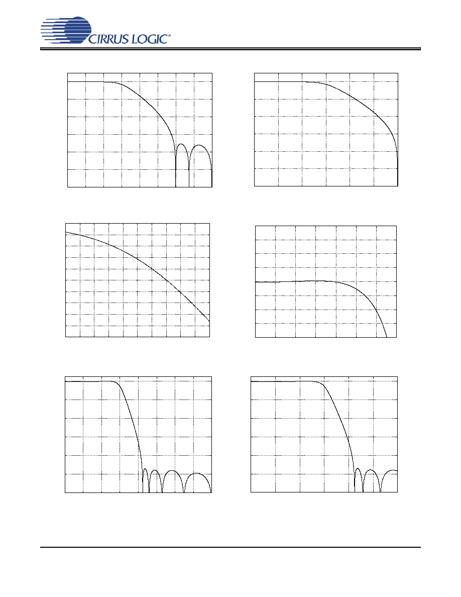
DS568F1
43
CS4398
0.2
0.3
0.4
0.5
0.6
0.7
0.8
0.9
1
120
100
80
60
40
20
0
Frequency(normalized to Fs)
Amplitude (dB)
0.2
0.3
0.4
0.5
0.6
0.7
0.8
120
100
80
60
40
20
0
Frequency(normalized to Fs)
Amplitude (dB)
Figure 32. Double-Speed (slow) Stopband Rejection
Figure 33. Double-Speed (slow) Transition Band
0.45
0.46
0.47
0.48
0.49
0.5
0.51
0.52
0.53
0.54
0.55
10
9
8
7
6
5
4
3
2
1
0
Frequency(normalized to Fs)
Amplitude (dB)
0
0.05
0.1
0.15
0.2
0.25
0.3
0.35
0.02
0.015
0.01
0.005
0
0.005
0.01
0.015
0.02
Frequency(normalized to Fs)
Amplitude (dB)
Figure 34. Double-Speed (slow) Transition Band (detail)
Figure 35. Double-Speed (slow) Passband Ripple
0.2
0.3
0.4
0.5
0.6
0.7
0.8
0.9
1
120
100
80
60
40
20
0
Frequency(normalized to Fs)
Amplitude (dB)
0.2
0.3
0.4
0.5
0.6
0.7
0.8
120
100
80
60
40
20
0
Frequency(normalized to Fs)
Amplitude (dB)
Figure 36. Quad-Speed (fast) Stopband Rejection
Figure 37. Quad-Speed (fast) Transition Band
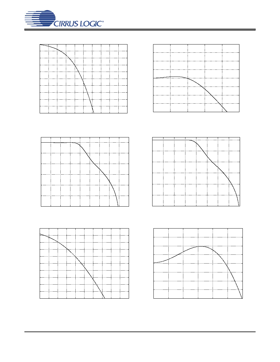
44
DS568F1
CS4398
0.45
0.46
0.47
0.48
0.49
0.5
0.51
0.52
0.53
0.54
0.55
10
9
8
7
6
5
4
3
2
1
0
Frequency(normalized to Fs)
Amplitude (dB)
0
0.05
0.1
0.15
0.2
0.25
0.2
0.15
0.1
0.05
0
0.05
0.1
0.15
0.2
Frequency(normalized to Fs)
Amplitude (dB)
Figure 38. Quad-Speed (fast) Transition Band (detail)
Figure 39. Quad-Speed (fast) Passband Ripple
0.1
0.2
0.3
0.4
0.5
0.6
0.7
0.8
0.9
1
120
100
80
60
40
20
0
Frequency(normalized to Fs)
Amplitude (dB)
0.1
0.2
0.3
0.4
0.5
0.6
0.7
0.8
0.9
120
100
80
60
40
20
0
Frequency(normalized to Fs)
Amplitude (dB)
Figure 40. Quad-Speed (slow) Stopband Rejection
Figure 41. Quad-Speed (slow) Transition Band
0.45
0.46
0.47
0.48
0.49
0.5
0.51
0.52
0.53
0.54
0.55
10
9
8
7
6
5
4
3
2
1
0
Frequency(normalized to Fs)
Amplitude (dB)
0
0.02
0.04
0.06
0.08
0.1
0.12
0.02
0.015
0.01
0.005
0
0.005
0.01
0.015
0.02
Frequency(normalized to Fs)
Amplitude (dB)
Figure 42. Quad-Speed (slow) Transition Band (detail)
Figure 43. Quad-Speed (slow) Passband Ripple

DS568F1
45
CS4398
Table 8. Revision Table
Release
Date
Changes
A1
November 2002
Initial Release
PP1
July 2003
-Updated Legal Notice on page 46.
-Moved Min/Max/Typ spec note from "ANALOG CHARACTERISTICS" (on
page 9) to "CHARACTERISTICS AND SPECIFICATIONS" on page 8.
-Changed heading "RECOMMENDED OPERATING CONDITIONS" to "SPECI-
FIED OPERATING CONDITIONS" on page 8.
-Updated Full-scale Output Specifications on page 9
-Updated FILT+ nominal Voltage Specification on page 17
-Added control port note to Table 1 on page 21
-Added 64x MCLK ratio note to Table 2 on page 22
-Changed default value of DIF0 in register 02h on page 28 and
-Updated the definition of the "Digital Volume Control (VOL7:0) Bits 7-0" on
page 34
PP2
February 2004
-Updated front page block diagram
-Updated front page THD+N spec
-Added Note for -CZZ package option
-Updated Legal Notice
-Corrected 768x mode in tables 1 and 2 to use MCLKDIV2
-Added note for 0 dB-SACD to ANALOG CHARACTERISTICS
-Updated Typ and Max THD+N specs
-Updated Full-scale output levels
-Updated VIL spec
-Updated VOH and VOL levels and conditions
-Updated Max sample rate specs
-Updated recommended FILT+ capacitor value in Typical Connection Diagram
-Corrected ATAPI table values 19d and 23d
PP3
September 2004
Updated DS w/ lead-free device ordering info.
PP4
May 2005
-Removed -CZ ordering option (PCN_0044 dated Jan. 2005)
-Improved Interchannel Isolation specification
-Updated analog output impedance
-Corrected Ramp_UP and Ramp_DN bit descriptions
-Updated legal text
F1
July 2005
-Changed datasheet status to Final
-Updated legal text

46
DS568F1
CS4398
Contacting Cirrus Logic Support
For all product questions and inquiries contact a Cirrus Logic Sales Representative.
To find one nearest you go to
www.cirrus.com
IMPORTANT NOTICE
Cirrus Logic, Inc. and its subsidiaries ("Cirrus") believe that the information contained in this document is accurate and reliable. However, the information is sub-
ject to change without notice and is provided "AS IS" without warranty of any kind (express or implied). Customers are advised to obtain the latest version of
relevant information to verify, before placing orders, that information being relied on is current and complete. All products are sold subject to the terms and con-
ditions of sale supplied at the time of order acknowledgment, including those pertaining to warranty, indemnification, and limitation of liability. No responsibility
is assumed by Cirrus for the use of this information, including use of this information as the basis for manufacture or sale of any items, or for infringement of
patents or other rights of third parties. This document is the property of Cirrus and by furnishing this information, Cirrus grants no license, express or implied
under any patents, mask work rights, copyrights, trademarks, trade secrets or other intellectual property rights. Cirrus owns the copyrights associated with the
information contained herein and gives consent for copies to be made of the information only for use within your organization with respect to Cirrus integrated
circuits or other products of Cirrus. This consent does not extend to other copying such as copying for general distribution, advertising or promotional purposes,
or for creating any work for resale.
CERTAIN APPLICATIONS USING SEMICONDUCTOR PRODUCTS MAY INVOLVE POTENTIAL RISKS OF DEATH, PERSONAL INJURY, OR SEVERE
PROPERTY OR ENVIRONMENTAL DAMAGE ("CRITICAL APPLICATIONS"). CIRRUS PRODUCTS ARE NOT DESIGNED, AUTHORIZED OR WARRANT-
ED FOR USE IN AIRCRAFT SYSTEMS, MILITARY APPLICATIONS, PRODUCTS SURGICALLY IMPLANTED INTO THE BODY, AUTOMOTIVE SAFETY OR
SECURITY DEVICES, LIFE SUPPORT PRODUCTS OR OTHER CRITICAL APPLICATIONS. INCLUSION OF CIRRUS PRODUCTS IN SUCH APPLICA-
TIONS IS UNDERSTOOD TO BE FULLY AT THE CUSTOMER'S RISK AND CIRRUS DISCLAIMS AND MAKES NO WARRANTY, EXPRESS, STATUTORY
OR IMPLIED, INCLUDING THE IMPLIED WARRANTIES OF MERCHANTABILITY AND FITNESS FOR PARTICULAR PURPOSE, WITH REGARD TO ANY
CIRRUS PRODUCT THAT IS USED IN SUCH A MANNER. IF THE CUSTOMER OR CUSTOMER'S CUSTOMER USES OR PERMITS THE USE OF CIRRUS
PRODUCTS IN CRITICAL APPLICATIONS, CUSTOMER AGREES, BY SUCH USE, TO FULLY INDEMNIFY CIRRUS, ITS OFFICERS, DIRECTORS, EM-
PLOYEES, DISTRIBUTORS AND OTHER AGENTS FROM ANY AND ALL LIABILITY, INCLUDING ATTORNEYS' FEES AND COSTS, THAT MAY RESULT
FROM OR ARISE IN CONNECTION WITH THESE USES.
Cirrus Logic, Cirrus, and the Cirrus Logic logo designs are trademarks of Cirrus Logic, Inc. All other brand and product names in this document may be trade-
marks or service marks of their respective owners.
SPI is a trademark of Motorola, Inc.