
Preliminary Product Information
This document contains information for a new product.
Cirrus Logic reserves the right to modify this product without notice.
Copyright
© Cirrus Logic, Inc. 2004
(All Rights Reserved)
http://www.cirrus.com
Features
1.8 to 3.3 Volt supply
24-Bit conversion / 96 kHz sample rate
96 dB dynamic range at 3 V supply
-85 dB THD+N
Low power consumption
Digital volume control
∑ 96 dB attenuation, 1 dB step size
Digital bass and treble boost
∑ Selectable corner frequencies
∑ Up to 12 dB boost in 1 dB increments
Peak signal limiting to prevent clipping
De-emphasis for 32 kHz, 44.1 kHz, and 48 kHz
Headphone amplifier
∑ up to 25 mW
rms
power output into 16
load*
∑ 25 dB analog attenuation and mute
∑ Zero crossing click free level transitions
ATAPI mixing functions
24-Pin TSSOP package
*
1 kHz sine wave at 3.3V supply
Description
The CS43L42 is a complete stereo digital-to-analog out-
put system including interpolation, 1-bit D/A conversion,
analog filtering, volume control, line level outputs, and a
headphone amplifier, in a 24-pin TSSOP package.
The CS43L42 is based on delta-sigma modulation,
where the modulator output controls the reference volt-
age input to an ultra-linear analog low-pass filter. This
architecture allows infinite adjustment of the sample rate
between 2 kHz and 100 kHz simply by changing the
master clock frequency.
The CS43L42 contains on-chip digital bass and treble
boost, peak signal limiting, and de-emphasis. The
CS43L42 operates from a +1.8 V to +3.3 V supply and
consumes only 16 mW of power with a 1.8 V supply with
the line amplifier powered-down. These features are
ideal for portable CD, MP3 and MD players and other
portable playback systems that require extremely low
power consumption.
ORDERING INFORMATION
CS43L42-KZ
-10 to 70 ∞C 24-pin TSSOP
CS43L42-KZZ, Lead Free -10 to 70 ∞C 24-pin TSSOP
CDB43L42
Evaluation Board
SCL/CCLK/DIF1 SDA/CDIN/DIF0 AD0/CS/DEM0
MUTEC
Control Port
Digital
Volume
Control
Bass/Treble
Boost
Limiting
Analog
Filter
Analog
Filter
HP_A
HP_B
AOUTA
AOUTB
RST
LRCK
SCLK/DEM1
SDATA
Se
ri
a
l
Po
r
t
De
-
e
m
p
h
a
s
i
s
D
i
g
i
ta
l
F
il
te
rs
DAC
DAC
H
e
ad
p
h
on
e
Amp
l
i
f
i
e
r
External
Mute Control
Analog
Volume
Control
MCLK
Analog
Volume
Control
Li
n
e
Am
p
l
i
f
i
e
r
Co
m
p
en
s
a
t
i
o
n
G
a
i
n
VA_HP
VA_LINE
VA
VL
GND
VQ_HP
FILT+
REF_GND
VQ_LINE
CS43L42
Low Voltage, Stereo DAC with Headphone Amp
Sep `04
DS481PP2

CS43L42
2
DS481PP2
TABLE OF CONTENTS
1. CHARACTERISTICS/SPECIFICATIONS ....................................................... 5
ANALOG CHARACTERISTICS................................................................... 5
ANALOG CHARACTERISTICS................................................................... 6
ANALOG CHARACTERISTICS................................................................... 7
POWER AND THERMAL CHARACTERISTICS ......................................... 8
DIGITAL CHARACTERISTICS.................................................................... 9
ABSOLUTE MAXIMUM RATINGS .............................................................. 9
RECOMMENDED OPERATING CONDITIONS .......................................... 9
SWITCHING CHARACTERISTICS ........................................................... 10
SWITCHING CHARACTERISTICS - CONTROL PORT - TWO-WIRE MODE12
SWITCHING CHARACTERISTICS - CONTROL PORT - SPI MODE....... 13
2. TYPICAL CONNECTION DIAGRAM .......................................................... 14
3. REGISTER QUICK REFERENCE ................................................................ 15
4. REGISTER DESCRIPTION .......................................................................... 16
4.1 Power and Muting Control (address 01h) .......................................... 16
4.1.1 Auto-mute (AMUTE) ........................................................................ 16
4.1.2 Soft Ramp AND Zero Cross CONTROL (SZC) ................................ 16
4.1.3 PopguardÆ Transient Control (POR)............................................... 17
4.1.4 Power Down Headphone Amplifier (PDNHP)................................... 17
4.1.5 Power Down Line Amplifier (PDNLN) ............................................... 17
4.1.6 Power Down (PDN) .......................................................................... 17
4.2 Channel A Analog Headphone Attenuation Control (address 02h) (HVOLA)18
4.3 Channel B Analog Headphone Attenuation Control (address 03h) (hVOLB)18
4.4 Channel A Digital Volume Control (address 04h) (DVOLA) ............... 18
4.5 Channel B Digital Volume Control (address 05h) (DVOLB) ............... 18
4.6 Tone Control (address 06h)................................................................ 19
4.6.1 Bass Boost Level (BB)...................................................................... 19
4.6.2 Treble Boost Level (tb) ..................................................................... 19
4.7 Mode Control (address 07h) ............................................................... 20
4.7.1 Bass Boost Corner Frequency (bbcf) ............................................... 20
4.7.2 Treble Boost Corner Frequency (TBCF)........................................... 20
4.7.3 Channel A Volume = Channel B Volume (A=B) ............................... 20
4.7.4 De-Emphasis Control (DEM) ............................................................ 21
4.7.5 Digital Volume Control Bypass (VCBYP).......................................... 21
4.8 Limiter Attack Rate (address 08h) (ARATE)....................................... 21
4.9 Limiter Release Rate (address 09h) (RRATE) ............................... 22
Contacting Cirrus Logic Support
For a complete listing of Direct Sales, Distributor, and Sales Representative contacts, visit the Cirrus Logic web site at:
http://www.cirrus.com/corporate/contacts/
I
2
C is a registered trademark of Philips Semiconductors.
Preliminary product information describes products which are in production, but for which full characterization data is not yet available. Advance product infor-
mation describes products which are in development and subject to development changes. Cirrus Logic, Inc. has made best efforts to ensure that the information
contained in this document is accurate and reliable. However, the information is subject to change without notice and is provided "AS IS" without warranty of
any kind (express or implied). No responsibility is assumed by Cirrus Logic, Inc. for the use of this information, nor for infringements of patents or other rights
of third parties. This document is the property of Cirrus Logic, Inc. and implies no license under patents, copyrights, trademarks, or trade secrets. No part of
this publication may be copied, reproduced, stored in a retrieval system, or transmitted, in any form or by any means (electronic, mechanical, photographic, or
otherwise) without the prior written consent of Cirrus Logic, Inc. Items from any Cirrus Logic website or disk may be printed for use by the user. However, no
part of the printout or electronic files may be copied, reproduced, stored in a retrieval system, or transmitted, in any form or by any means (electronic, mechanical,
photographic, or otherwise) without the prior written consent of Cirrus Logic, Inc.Furthermore, no part of this publication may be used as a basis for manufacture
or sale of any items without the prior written consent of Cirrus Logic, Inc. The names of products of Cirrus Logic, Inc. or other vendors and suppliers appearing
in this document may be trademarks or service marks of their respective owners which may be registered in some jurisdictions. A list of Cirrus Logic, Inc. trade-
marks and service marks can be found at http://www.cirrus.com.

CS43L42
DS481PP2
3
4.10 Volume and Mixing Control (address 0Ah)....................................... 22
4.10.1 Tone Control MODE (TC)............................................................... 22
4.10.2 Tone Control Enable (TC_EN) ....................................................... 22
4.10.3 Peak Signal Limiter Enable (LIM_EN)............................................ 23
4.10.4 ATAPI Channel Mixing and Muting (atapi) ..................................... 23
4.11 Mode Control 2 (address 0Bh) ......................................................... 24
4.11.1 Master Clock DIVIDE ENABLE (mclkdiv)....................................... 24
4.11.2 Line Amplifier Gain Compensation (line)........................................ 24
4.11.3 Digital Interface Format (dif)........................................................... 24
5. PIN DESCRIPTION ....................................................................................... 26
6. APPLICATIONS ........................................................................................... 29
6.1 Grounding and Power Supply Decoupling ........................................ 29
6.2 Clock Modes ...................................................................................... 29
6.3 De-Emphasis ..................................................................................... 29
6.4 Recommended Power-up Sequence ................................................ 29
6.5 PopGuardÆ Transient Control ........................................................... 29
7. CONTROL PORT INTERFACE .................................................................... 30
7.1 SPI Mode ........................................................................................... 30
7.2 Two-Wire Mode ................................................................................. 30
7.3 Memory Address Pointer (MAP) ............................................... 31
7.3.1 INCR (Auto Map Increment Enable)................................................. 31
7.3.2 MAP0-3 (Memory Address Pointer) ................................................. 31
8. PARAMETER DEFINITIONS ........................................................................ 39
9. REFERENCES .............................................................................................. 39
10. PACKAGE DIMENSIONS ......................................................................... 40
LIST OF FIGURES
Figure 1. External Serial Mode Input Timing ............................................................ 11
Figure 2. Internal Serial Mode Input Timing ............................................................. 11
Figure 3. Internal Serial Clock Generation ............................................................... 11
Figure 4. Control Port Timing - Two-Wire Mode ....................................................... 12
Figure 5. Control Port Timing - SPI Mode ................................................................ 13
Figure 6. Typical Connection Diagram ..................................................................... 14
Figure 7. Control Port Timing, SPI mode .................................................................. 31
Figure 8. Control Port Timing, Two-Wire Mode ........................................................ 31
Figure 9. Base-Rate Stopband Rejection ................................................................. 32
Figure 10. Base-Rate Transition Band ..................................................................... 32
Figure 11. Base-Rate Transition Band (Detail) ......................................................... 32
Figure 12. Base-Rate Passband Ripple ................................................................... 32
Figure 13. High-Rate Stopband Rejection ................................................................ 32
Figure 14. High-Rate Transition Band ...................................................................... 32
Figure 15. High-Rate Transition Band (Detail) ......................................................... 33
Figure 16. High-Rate Passband Ripple .................................................................... 33
Figure 17. Line Output Test Load ............................................................................. 33
Figure 18. Headphone Output Test Load ................................................................. 33
Figure 19. CS43L42 Control Port Mode - Serial Audio Format 0 ............................. 34
Figure 20. CS43L42 Control Port Mode - Serial Audio Format 1 ............................. 34
Figure 21. CS43L42 Control Port Mode - Serial Audio Format 2 ............................. 34
Figure 22. CS43L42 Control Port Mode - Serial Audio Format 3 ............................. 35
Figure 23. CS43L42 Control Port Mode - Serial Audio Format 4 ............................. 35
Figure 24. CS43L42 Control Port Mode - Serial Audio Format 5 ............................. 35
Figure 25. CS43L42 Control Port Mode - Serial Audio Format 6 ............................. 36
Figure 26. CS43L42 Stand Alone Mode - Serial Audio Format 0 ............................. 36

CS43L42
4
DS481PP2
Figure 27. CS43L42 Stand Alone Mode - Serial Audio Format 1 ............................. 36
Figure 28. CS43L42 Stand Alone Mode - Serial Audio Format 2 ............................. 37
Figure 29. CS43L42 Stand Alone Mode - Serial Audio Format 3 ............................. 37
Figure 30. De-Emphasis Curve ................................................................................. 38
Figure 31. ATAPI Block Diagram .............................................................................. 38
LIST OF TABLES
Table 1. Example Analog Volume Settings ............................................................... 18
Table 2. Example Digital Volume Settings ................................................................ 19
Table 3. Example Bass Boost Settings ..................................................................... 19
Table 4. Example Treble Boost Settings ................................................................... 19
Table 5. Example Limiter Attack Rate Settings ......................................................... 21
Table 6. Example Limiter Release Rate Settings ..................................................... 22
Table 7. ATAPI Decode ............................................................................................ 23
Table 8. Digital Interface Format ............................................................................... 25
Table 9. Stand Alone De-Emphasis Control ............................................................. 27
Table 10. HRM Common Clock Frequencies ........................................................... 27
Table 11. BRM Common Clock Frequencies ............................................................ 27
Table 12. Digital Interface Format - DIF1 and DIF0 (Stand-Alone Mode) ................ 28
Table 13.

CS43L42
DS481PP2
5
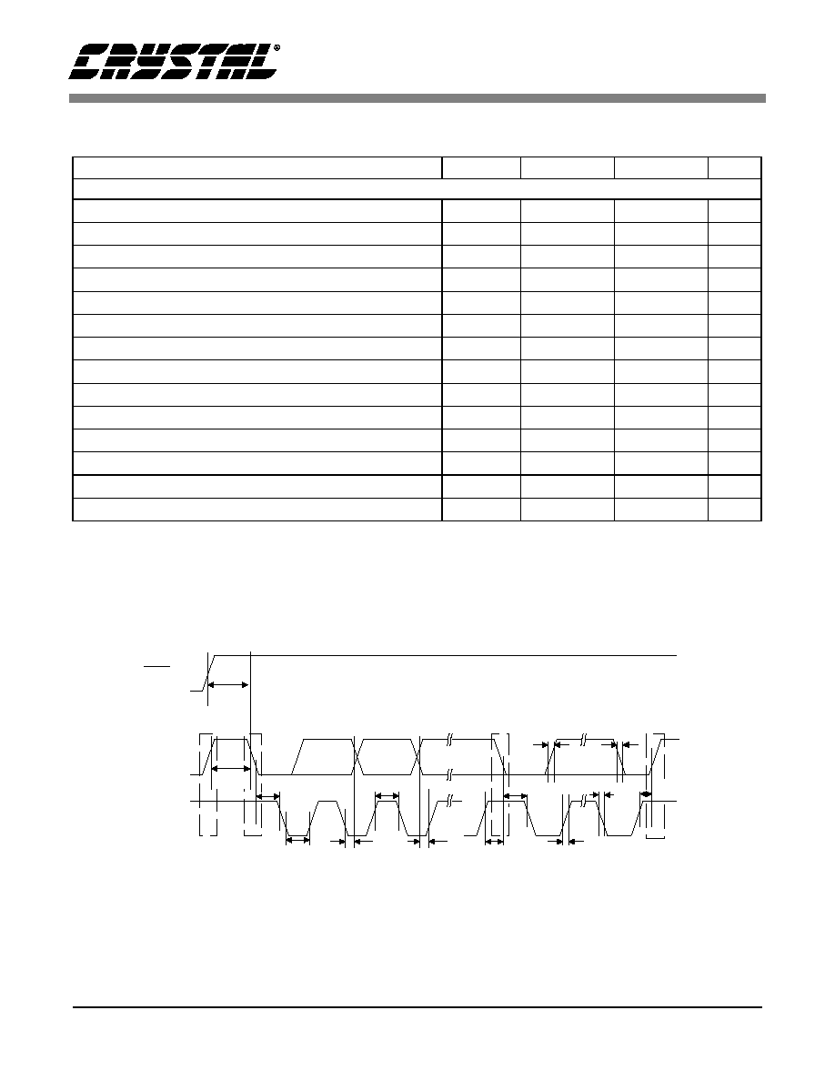
1. CHARACTERISTICS/SPECIFICATIONS
ANALOG CHARACTERISTICS
(T
A
= 25∞ C; Logic "1" = VL = 1.8 V; Logic "0" = GND = 0 V;
Full-Scale Output Sine Wave, 997 Hz; MCLK = 12.288 MHz; Measurement Bandwidth 10 Hz to 20 kHz, unless oth-
erwise specified; Fs for Base-rate Mode = 48 kHz, SCLK = 3.072 MHz. Fs for High-Rate Mode = 96 kHz,
SCLK = 6.144 MHz. Test load R
L
= 10 k
, C
L
= 10 pF (see Figure 17) for line out, R
L
= 16
, C
L
= 10 pF (see Fig-
ure 18) for headphone out).
Notes: 1. One-half LSB of triangular PDF dither is added to data.
Parameter
Base-rate Mode
High-Rate Mode
Symbol
Min
Typ
Max
Min
Typ
Max
Unit
Line Output Dynamic Performance for VA = VA_LINE = 1.8 V
Dynamic Range
(Note 1)
18 to 24-Bit
unweighted
A-Weighted
16-Bit
unweighted
A-Weighted
TBD
TBD
-
-
91
94
89
92
-
-
-
-
TBD
TBD
-
-
89
92
87
90
-
-
-
-
dB
dB
dB
dB
Total Harmonic Distortion + Noise
(Note 1)
18 to 24-Bit
0 dB
-20 dB
-60 dB
16-Bit
0 dB
-20 dB
-60 dB
THD+N
-
-
-
-
-
-
-80
-71
-31
-78
-69
-29
TBD
-
-
-
-
-
-
-
-
-
-
-
-80
-69
-29
-78
-67
-27
TBD
-
-
-
-
-
dB
dB
dB
dB
dB
dB
Interchannel Isolation
(1 kHz)
-
100
-
-
100
-
dB
Headphone Output Dynamic Performance for VA = VA_HP = 1.8 V
Dynamic Range
(Note 1)
18 to 24-Bit
unweighted
A-Weighted
16-Bit
unweighted
A-Weighted
TBD
TBD
-
-
88
91
86
89
-
-
-
-
TBD
TBD
-
-
88
91
86
89
-
-
-
-
dB
dB
dB
dB
Total Harmonic Distortion + Noise
(Note 1)
18 to 24-Bit
0 dB
-20 dB
-60 dB
16-Bit
0 dB
-20 dB
-60 dB
THD+N
-
-
-
-
-
-
-82
-68
-28
-80
-66
-26
TBD
-
-
-
-
-
-
-
-
-
-
-
-85
-68
-28
-83
-66
-26
TBD
-
-
-
-
-
dB
dB
dB
dB
dB
dB
Interchannel Isolation
(1 kHz)
-
66
-
-
66
-
dB

CS43L42
6
DS481PP2
ANALOG CHARACTERISTICS
(Continued)
Parameter
Base-rate Mode
High-Rate Mode
Symbol
Min
Typ
Max
Min
Typ
Max
Unit
Line Output Dynamic Performance for VA = VA_LINE = 3.0 V
Dynamic Range.
(Note 1)
18 to 24-Bit.
unweighted
A-Weighted
16-Bit. unweighted
A-Weighted
TBD
TBD
-
-
93
96
91
94
-
-
-
-
TBD
TBD
-
-
93
96
91
94
-
-
-
-
dB
dB
dB
dB
Total Harmonic Distortion + Noise.
(Note 1)
18 to 24-Bit.
0 dB
-20 dB
-60 dB
16-Bit. 0 dB
-20 dB
-60 dB
THD+N
-
-
-
-
-
-
-85
-73
-33
-83
-71
-31
TBD
-
-
-
-
-
-
-
-
-
-
-
-85
-73
-33
-83
-71
-31
TBD
-
-
-
-
-
dB
dB
dB
dB
dB
dB
Interchannel Isolation.
(1 kHz)
-
100
-
-
100
-
dB
Headphone Output Dynamic Performance for VA = VA_HP = 3.0 V
Dynamic Range.
(Note 1)
18 to 24-Bit.
unweighted
A-Weighted
16-Bit. unweighted
A-Weighted
TBD
TBD
-
-
90
93
88
91
-
-
-
-
TBD
TBD
-
-
90
93
88
91
-
-
-
-
dB
dB
dB
dB
Total Harmonic Distortion + Noise.
(Note 1)
18 to 24-Bit.
0 dB
-20 dB
-60 dB
16-Bit. 0 dB
-20 dB
-60 dB
THD+N
-
-
-
-
-
-
-76
-70
-30
-74
-68
-28
TBD
-
-
-
-
-
-
-
-
-
-
-
-73
-70
-30
-71
-68
-28
TBD
-
-
-
-
-
dB
dB
dB
dB
dB
dB
Interchannel Isolation.
(1 kHz)
-
66
-
-
66
-
dB

CS43L42
DS481PP2
7
ANALOG CHARACTERISTICS
(Continued)
Notes: 2. See Line Amplifier Gain Compensation (line) for details.
3. Filter response is not tested but is guaranteed by design.
4. Response is clock dependent and will scale with Fs. Note that the response plots (Figures 9-16) have
been normalized to Fs and can be de-normalized by multiplying the X-axis scale by Fs.
5. Referenced to a 1 kHz, full-scale sine wave.
6. For Base-Rate Mode, the measurement bandwidth is 0.5465 Fs to 3 Fs.
For High-Rate Mode, the measurement bandwidth is 0.577 Fs to 1.4 Fs.
7. De-emphasis is not available in High-Rate Mode.
Parameters
Symbol
Min
Typ
Max
Units
Analog Output
Full Scale Line Output Voltage
(Note 2) V
FS_LINE
TBD
G x VA
TBD
Vpp
Line Output Quiescent Voltage
V
Q_LINE
-
0.5 x VA_LINE
-
VDC
Full Scale Headphone Output Voltage
V
FS_HP
TBD
0.55 x VA
TBD
Vpp
Headphone Output Quiescent Voltage
V
Q_HP
-
0.5 x VA_HP
-
VDC
Interchannel Gain Mismatch
-
0.1
-
dB
Gain Drift
-
100
-
ppm/∞C
Maximum Line Output AC-Current
VA=VA_LINE=1.8 V
VA=VA_LINE=3.0 V
I
LINE
-
-
0.1
0.15
-
-
mA
mA
Maximum Headphone Output
VA=VA_HP=1.8 V
AC-Current
VA=VA_HP=3.0 V
I
HP
-
-
31
52
-
-
mA
mA
Parameter
Base-rate Mode
High-Rate Mode
Symbol
Min
Typ
Max
Min
Typ
Max
Unit
Combined Digital and On-chip Analog Filter Response (Note 3)
Passband
(Note 4)
to -0.05 dB corner
to -0.1 dB corner
to -3 dB corner
0
-
0
-
-
-
.4535
-
.4998
-
0
0
-
-
-
-
.4426
.4984
Fs
Fs
Fs
Frequency Response 10 Hz to 20 kHz
(Note 5)
-.02
-
+.08
0
-
+0.11
dB
StopBand
.5465
-
-
.577
-
-
Fs
StopBand Attenuation
(Note 6)
50
-
-
55
-
-
dB
Group Delay
tgd
-
9/Fs
-
-
4/Fs
-
s
Passband Group Delay Deviation 0 - 40 kHz
0 - 20 kHz
-
-
-
±0.36/Fs
-
-
-
-
±1.39/Fs
±0.23/Fs
-
-
s
s
De-emphasis Error
Fs = 32 kHz
(Relative to 1 kHz)
Fs = 44.1 kHz
Fs = 48 kHz
-
-
-
-
-
-
+.2/-.1
+.05/-.14
+0/-.22
(Note 7)
dB
dB
dB

CS43L42
8
DS481PP2
POWER AND THERMAL CHARACTERISTICS
(GND = 0 V; All voltages with respect to
ground. All measurements taken with all zeros input and open outputs, unless otherwise specified.)
Notes: 8. Power Down Mode is defined as RST = LO with all clocks and data lines held static.
9. Valid with the recommended capacitor values on FILT+, VQ_LINE and VQ_HP as shown in Figure 6.
Increasing the capacitance will also increase the PSRR. Note that care should be taken when selecting
capacitor type, as any leakage current in excess of 1.0 µA will cause degradation in analog
performance.
Parameters
Symbol
Min
Typ
Max
Units
Power Supplies
Power Supply Current-
VA=1.8 V
Normal Operation
VA_HP=1.8 V
VA_LINE=1.8 V
VL=1.8 V
I
A
I
A_HP
I
A_LINE
I
D_L
-
-
-
-
7.3
1.5
1.6
4
-
-
-
-
mA
mA
mA
µA
Power Supply Current-
VA=1.8 V
Power Down Mode (Note 8)
VA_HP=1.8 V
VA_LINE=1.8 V
VL=1.8 V
I
A
I
A_HP
I
A_LINE
I
D_L
-
-
-
-
TBD
TBD
TBD
TBD
-
-
-
-
µA
µA
µA
µA
Power Supply Current-
VA=3.0 V
Normal Operation
VA_HP=3.0 V
VA_LINE=3.0 V
VL=3.0 V
I
A
I
A_HP
I
A_LINE
I
D_L
-
-
-
-
10.5
1.5
1.7
9.3
-
-
-
-
mA
mA
mA
µA
Power Supply Current-
VA=3.0 V
Power Down Mode (Note 8)
VA_HP=3.0 V
VA_LINE=3.0 V
VL=3.0 V
I
A
I
A_HP
I
A_LINE
I
D_L
-
-
-
-
TBD
TBD
TBD
TBD
-
-
-
-
µA
µA
µA
µA
Total Power Dissipation-
All Supplies=1.8 V
Normal Operation
All Supplies=3.0 V
-
-
19
41
TBD
TBD
mW
mW
Maximum Headphone Power Dissipation
(1 kHz full-scale sine wave
VA=1.8 V
into 16 ohm load)
VA=3.0 V
-
-
TBD
TBD
-
-
mW
mW
Package Thermal Resistance
JA
-
75
-
∞C/Watt
Power Supply Rejection Ratio (Note 9)
(1 kHz)
(60 Hz)
PSRR
-
-
60
40
-
-
dB
dB

CS43L42
DS481PP2
9
DIGITAL CHARACTERISTICS
(T
A
= 25∞ C; VL = 1.7 V - 3.6 V; GND = 0 V)
ABSOLUTE MAXIMUM RATINGS
(GND = 0V; all voltages with respect to ground.)
WARNING: Operation at or beyond these limits may result in permanent damage to the device. Normal operation is
not guaranteed at these extremes.
RECOMMENDED OPERATING CONDITIONS
(GND = 0V; all voltages with respect to ground.)
Notes: 10. To prevent clipping the outputs, VA_HP
MIN
is limited by the Full-Scale Output Voltage V
FS_HP
, where
VA_HP must be 200 mV greater than V
FS_HP
. However, if distortion is not a concern, VA_HP may be
as low as 0.9 V at any time.
Parameters
Symbol Min Typ
Max
Units
High-Level Input Voltage
V
IH
0.7 x VL
-
-
V
Low-Level Input Voltage
V
IL
-
-
0.3 x VL
V
Input Leakage Current
I
in
-
-
±10
µA
Input Capacitance
-
8
-
pF
Maximum MUTEC Drive Capability
VA=1.8 V
VA=3.0 V
-
-
TBD
3
-
-
mA
mA
MUTEC High-Level Output Voltage
-
VA
-
V
MUTEC Low-Level Output Voltage
-
0
-
V
Parameters
Symbol
Min
Max
Units
DC Power Supplies:
Positive Analog
Headphone
Line
Digital I/O
VA
VA_HP
VA_LINE
VL
-0.3
-0.3
-0.3
-0.3
4.0
4.0
4.0
4.0
V
V
V
V
Input Current, Any Pin Except Supplies
I
in
-
±10
mA
Digital Input Voltage
V
IND
-0.3
VL+0.4
V
Ambient Operating Temperature (power applied)
T
A
-55
125
∞C
Storage Temperature
T
stg
-65
150
∞C
Parameters
Symbol Min Typ
Max
Units
Ambient Temperature
T
A
-10
-
70
∞C
DC Power Supplies:
Positive Analog
Headphone
(Note 10)
Line
Digital I/O
VA
VA_HP
VA_LINE
VL
1.7
0.9
VA
1.7
-
-
-
-
3.6
3.6
3.6
3.6
V
V
V
V

CS43L42
10
DS481PP2
SWITCHING CHARACTERISTICS
(T
A
= -10 to 70∞ C; VL = 1.7 V - 3.6 V; Inputs: Logic 0 = GND,
Logic 1 = VL, C
L
= 20 pF)
Notes: 11. Internal SCLK Mode timing is not tested, but is guaranteed by design.
12. In Internal SCLK Mode, the LRCK duty cycle must be 50%
+/- 1/2 MCLK Period.
Parameters
Symbol Min Typ
Max
Units
Input Sample Rate
Base Rate Mode
High Rate Mode
Fs
Fs
2
50
-
-
50
100
kHz
kHz
MCLK Pulse Width High
MCLK/LRCK = 1024
7
-
-
ns
MCLK Pulse Width Low
MCLK/LRCK = 1024
7
-
-
ns
MCLK Pulse Width High
MCLK/LRCK = 768
10
-
-
ns
MCLK Pulse Width Low
MCLK/LRCK = 768
10
-
-
ns
MCLK Pulse Width High
MCLK/LRCK = 512
15
-
-
ns
MCLK Pulse Width Low
MCLK/LRCK = 512
15
-
-
ns
MCLK Pulse Width High MCLK / LRCK = 384 or 192
25
-
-
ns
MCLK Pulse Width Low MCLK / LRCK = 384 or 192
25
-
-
ns
MCLK Pulse Width High MCLK / LRCK = 256 or 128
35
-
-
ns
MCLK Pulse Width Low MCLK / LRCK = 256 or 128
35
-
-
ns
External SCLK Mode
LRCK Duty Cycle (External SCLK only)
40
50
60
%
SCLK Pulse Width Low
t
sclkl
20
-
-
ns
SCLK Pulse Width High
t
sclkh
20
-
-
ns
SCLK Period
Base Rate Mode
t
sclkw
-
-
ns
High Rate Mode
t
sclkw
-
-
ns
SCLK rising to LRCK edge delay
t
slrd
20
-
-
ns
SCLK rising to LRCK edge setup time
t
slrs
20
-
-
ns
SDATA valid to SCLK rising setup time
t
sdlrs
20
-
-
ns
SCLK rising to SDATA hold time
t
sdh
20
-
-
ns
Internal SCLK Mode (Note 11)
LRCK Duty Cycle (Internal SCLK only)
(Note 12)
-
50
-
%
SCLK Period
t
sclkw
-
-
ns
SCLK rising to LRCK edge
t
sclkr
-
-
µs
SDATA valid to SCLK rising setup time
t
sdlrs
-
-
ns
SCLK rising to SDATA hold time
Base Rate Mode
t
sdh
-
-
ns
High Rate Mode
t
sdh
-
-
ns
1
128
(
)Fs
----------------------
1
64
(
)Fs
-------------------
1
SCLK
-----------------
tsclkw
2
------------------
1
512
(
)Fs
---------------------- 10
+
1
512
(
)Fs
---------------------- 15
+
1
384
(
)Fs
---------------------- 15
+

CS43L42
DS481PP2
11
sclkh
t
slrs
t
slrd
t
s d lrs
t
sd h
t
sclkl
t
S D A T A
S C LK
L R C K
Figure 1. External Serial Mode Input Timing
Figure 2. Internal Serial Mode Input Timing
*The SCLK pulses shown are internal to the CS43L42.
S D A T A
* IN T E R N A L
S C L K
L R C K
s c lk w
t
s d lrs
t
s d h
t
s c lk r
t
S D A T A
LR C K
M C LK
*IN T E R N A L S C LK
1
N
2
N
Figure 3. Internal Serial Clock Generation
* The SCLK pulses shown are internal to the CS43L42.
N equals MCLK divided by SCLK
CS43L42
12
DS481PP2
SWITCHING CHARACTERISTICS - CONTROL PORT - TWO-WIRE MODE
(T
A
= 25∞ C; VL = 1.7 V - 3.6 V; Inputs: Logic 0 = GND, Logic 1 = VL, C
L
= 30 pF)
Notes: 13. The Two-Wire Mode is compatible with the I
2
C protocol.
14. Data must be held for sufficient time to bridge the transition time, t
fc
, of SCL.
Parameter
Symbol
Min
Max
Unit
Two-Wire Mode (Note 13)
SCL Clock Frequency
f
scl
-
100
kHz
RST Rising Edge to Start
t
irs
500
-
ns
Bus Free Time Between Transmissions
t
buf
4.7
-
µs
Start Condition Hold Time (prior to first clock pulse)
t
hdst
4.0
-
µs
Clock Low time
t
low
4.7
-
µs
Clock High Time
t
high
4.0
-
µs
Setup Time for Repeated Start Condition
t
sust
4.7
-
µs
SDA Hold Time from SCL Falling
(Note 14)
t
hdd
0
-
µs
SDA Setup time to SCL Rising
t
sud
250
-
ns
Rise Time of SCL
t
rc
-
25
ns
Fall Time SCL
t
fc
-
25
ns
Rise Time of SDA
t
rd
1
µs
Fall Time of SDA
t
fd
300
ns
Setup Time for Stop Condition
t
susp
4.7
-
µs
t
b u f
t
h d st
t
h ds t
t
l o w
t
rc
t
fc
t
h d d
t
h ig h
t
s u d
t sust
t susp
S to p
S t a r t
S t a r t
S to p
R e p e a t e d
S D A
S C L
t
irs
R S T
t
rd
t
fd
Figure 4. Control Port Timing - Two-Wire Mode

CS43L42
DS481PP2
13
SWITCHING CHARACTERISTICS - CONTROL PORT - SPI MODE
(T
A
= 25∞ C; VL = 1.7 V - 3.6 V; Inputs: Logic 0 = GND, Logic 1 = VL, C
L
= 30 pF)
Notes: 15. t
spi
only needed before first falling edge of CS after RST rising edge. t
spi
= 0 at all other times.
16. Data must be held for sufficient time to bridge the transition time of CCLK.
17. For F
SCK
< 1 MHz
Parameter
Symbol
Min
Max
Unit
SPI Mode
CCLK Clock Frequency
f
sclk
-
6
MHz
RST Rising Edge to CS Falling
t
srs
500
-
ns
CCLK Edge to CS Falling
(Note 15)
t
spi
500
-
ns
CS High Time Between Transmissions
t
csh
1.0
-
µs
CS Falling to CCLK Edge
t
css
20
-
ns
CCLK Low Time
t
scl
66
-
ns
CCLK High Time
t
sch
66
-
ns
CDIN to CCLK Rising Setup Time
t
dsu
40
-
ns
CCLK Rising to DATA Hold Time
(Note 16)
t
dh
15
-
ns
Rise Time of CCLK and CDIN
(Note 17)
t
r2
-
100
ns
Fall Time of CCLK and CDIN
(Note 17)
t
f2
-
100
ns
t r2
t f2
t dsu t
d h
t
s ch
t scl
C S
C C L K
C D IN
t css
t
c s h
t spi
t srs
R S T
Figure 5. Control Port Timing - SPI Mode

CS43L42
14
DS481PP2
2. TYPICAL CONNECTION DIAGRAM
MCLK
LRCK
SCLK/DEM1
SDATA
CP/SA
RST
SDA/CDIN/DIF0
SCL/CCLK/DIF1
AD0/CS/DEM0
µc/
Digital
Audio
Source
VA
VA_HP
HP_A
HP_B
AOUTA
AOUTB
MUTEC
CS43 42
16
Headphones
1.8 to 3.3 V
Supply
*Ferrite
bead
1.0 µF
0.1 µF
+
+
Mute
Circuit
VA_LINE
0.9 to 3.3 V
Supply
*Ferrite
bead
220
220
3.3 µF
3.3 µF
10k
10k
560
560
C
C
1.8 to 3.3 V
Supply
1.0 µF
0.1 µF
+
VL
*Ferrite
bead
R
L
R
L
Audio
Output A
Audio
Output B
+
+
+
+
18
19
20
6
7
2
5
3
16
21
23
11
1
9
8
22
24
4
17
4.7 µH
4.7 µH
Mode
Configuration
1k
1k
*
*
*
µF
µF
0.1 µF
GND
1.0 µF
* Optional
L
C =
4 Fs(R
L
+ 560
R
L
560)
VQ_HP
VQ_LINE
FILT+
REF_GND
1.0 µF
+
12
15
14
13
1.0 µF
+
1.0 µF
+
Figure 6. Typical Connection Diagram

CS43L42
DS481PP2
15
3. REGISTER QUICK REFERENCE
Addr
Function
7
6
5
4
3
2
1
0
0h
Reserved
Reserved Reserved Reserved Reserved Reserved Reserved Reserved Reserved
default
0
0
0
0
0
0
0
0
1h
Power and Muting
Control
AMUTE
SZC1
SZC0
POR
PDNHP
PDNLN
PDN
Reserved
default
1
1
0
1
0
0
1
0
2h
Channel A Analog
Headphone
Attenuation Control
HVOLA7
HVOLA6
HVOLA5
HVOLA4
HVOLA3
HVOLA2
HVOLA1
HVOLA0
default
0
0
0
0
0
0
0
0
3h
Channel B Analog
Headphone
Attenuation Control
HVOLB7
HVOLB6
HVOLB5
HVOLB4
HVOLB3
HVOLB2
HVOLB1
HVOLB0
default
0
0
0
0
0
0
0
0
4h
Channel A Digital
Volume Control
DVOLA7
DVOLA6
DVOLA5
DVOLA4
DVOLA3
DVOLA2
DVOLA1
DVOLA0
default
0
0
0
0
0
0
0
0
5h
Channel B Digital
Volume Control
DVOLB7
DVOLB6
DVOLB5
DVOLB4
DVOLB3
DVOLB2
DVOLB1
DVOLB0
default
0
0
0
0
0
0
0
0
6h
Tone Control
BB3
BB2
BB1
BB0
TB3
TB2
TB1
TB0
default
0
0
0
0
0
0
0
0
7h
Mode Control
BBCF1
BBCF0
TBCF1
TBCF0
A=B
DEM1
DEM0
VCBYP
default
0
0
0
0
0
0
0
0
8h
Limiter Attack Rate
ARATE7
ARATE6
ARATE5
ARATE4
ARATE3
ARATE2
ARATE1
ARATE0
default
0
0
0
1
0
0
0
0
9h
Limiter Release Rate
RRATE7
RRATE6
RRATE5
RRATE4
RRATE3
RRATE2
RRATE1
RRATE0
default
0
0
1
0
0
0
0
0
Ah
Volume and Mixing
Control
TC1
TC0
TC_EN
LIM_EN
ATAPI3
ATAPI2
ATAPI1
ATAPI0
default
0
0
0
0
1
0
0
1
Bh
Mode Control 2
MCLKDIV
LINE1
LINE0
Reserved Reserved
DIF2
DIF1
DIF0
default
0
0
0
0
0
0
0
0

CS43L42
16
DS481PP2
4. REGISTER DESCRIPTION
Note:
All registers are read/write in Two-Wire mode and write only in SPI, unless otherwise noted.
4.1 Power and Muting Control (address 01h)
4.1.1 AUTO-MUTE (AMUTE)
Default = 1
0 - Disabled
1 - Enabled
Function:
The Digital-to-Analog converter output will mute following the reception of 8192 consecutive audio sam-
ples of static 0 or -1. A single sample of non-static data will release the mute. Detection and muting is
done independently for each channel. The quiescent voltage on the output will be retained and the Mute
Control pin will go active during the mute period. The muting function is affected, similar to volume control
changes, by the Soft and Zero Cross bits in the Power and Muting Control register.
4.1.2 SOFT RAMP AND ZERO CROSS CONTROL (SZC)
Default = 10
00 - Immediate Change
01 - Zero Cross Digital and Analog
10 - Ramped Digital and Analog
11 - Reserved
Function:
Immediate Change
When Immediate Change is selected all level changes will take effect immediately in one step.
Zero Cross Digital and Analog
Zero Cross Enable dictates that signal level changes, either by attenuation changes or muting, will occur
on a signal zero crossing to minimize audible artifacts. The requested level change will occur after a
timeout period of 512 sample periods (10.7 ms at 48 kHz sample rate) if the signal does not encounter a
zero crossing. The zero cross function is independently monitored and implemented for each channel.
Ramped Digital and Analog
Soft Ramp allows digital level changes, both muting and attenuation, to be implemented by incrementally
ramping, in 1/8 dB steps, from the current level to the new level at a rate of 1 dB per 8 left/right clock pe-
riods. Analog level changes will occur in 1 dB steps on a signal zero crossing. The analog level change
will occur after a timeout period of 512 sample periods (10.7 ms at 48 kHz sample rate) if the signal does
not encounter a zero crossing. The zero cross function is independently monitored and implemented for
each channel.
Note:
Ramped Digital and Analog is not available in High-Rate Mode.
7
6
5
4
3
2
1
0
AMUTE
SZC1
SZC0
POR
PDNHP
PDNLN
PDN
RESERVED
1
1
0
1
0
0
1
0

CS43L42
DS481PP2
17
4.1.3 POPGUARDÆ TRANSIENT CONTROL (POR)
Default - 1
0 - Disabled
1 - Enabled
Function:
The PopGuard
Æ
Transient Control allows the quiescent voltage to slowly ramp to and from 0 volts to the
quiescent voltage during power-on or power-off when this function is enabled. Please see section 6.5 for
implementation details.
4.1.4 POWER DOWN HEADPHONE AMPLIFIER (PDNHP)
Default = 0
0 - Disabled
1 - Enabled
Function:
The headphone amplifier will independently enter a low-power state when this function is enabled.
4.1.5 POWER DOWN LINE AMPLIFIER (PDNLN)
Default = 0
0 - Disabled
1 - Enabled
Function:
The line output amplifier will independently enter a low-power state when this function is enabled.
4.1.6 POWER DOWN (PDN)
Default = 1
0 - Disabled
1 - Enabled
Function:
The entire device will enter a low-power state when this function is enabled, and the contents of the control
registers are retained in this mode. The power-down bit defaults to `enabled' on power-up and must be
disabled before normal operation will begin.

CS43L42
18
DS481PP2
4.2 Channel A Analog Headphone Attenuation Control (address 02h) (HVOLA)
4.3 Channel B Analog Headphone Attenuation Control (address 03h) (hVOLB)
Default = 0 dB (No attenuation)
Function:
The Analog Headphone Attenuation Control operates independently from the Digital Volume Control. The
Analog Headphone Attenuation Control registers allow attenuation of the headphone output signal for
each channel in 1 dB increments from 0 to -25 dB. Attenuation settings are decoded using a 2's comple-
ment code, as shown in Table 1. The volume changes are implemented as dictated by the Soft and Zero
Cross bits in the Power and Muting Control register. All volume settings greater than zero are interpreted
as zero.
Note:
The Analog Headphone Attenuation only affects the headphone outputs.
4.4 Channel A Digital Volume Control (address 04h) (DVOLA)
4.5 Channel B Digital Volume Control (address 05h) (DVOLB)
Default = 0 dB (No attenuation)
Function:
The Digital Volume Control registers allow independent control of the signal levels in 1 dB increments
from +18 to -96 dB. Volume settings are decoded using a 2's complement code, as shown in Table 2.
The volume changes are implemented as dictated by the Soft and Zero Cross bits in the Power and Mut-
ing Control register. All volume settings less than -96 dB are equivalent to muting the channel via the
ATAPI bits (see Section 4.10.4).
Note:
The digital volume control affects both the line outputs and the headphone outputs. Setting this
register to values greater than +18 dB will cause distortion in the audio outputs.
7
6
5
4
3
2
1
0
HVOLx7
HVOLx6
HVOLx5
HVOLx4
HVOLx3
HVOLx2
HVOLx1
HVOLx0
0
0
0
0
0
0
0
0
Binary Code
Decimal Value
Volume Setting
00000000
0
0 dB
11110110
-10
-10 dB
11110001
-15
-15 dB
Table 1. Example Analog Volume Settings
7
6
5
4
3
2
1
0
DVOLx7
DVOLx6
DVOLx5
DVOLx4
DVOLx3
DVOLx2
DVOLx1
DVOLx0
0
0
0
0
0
0
0
0
CS43L42
DS481PP2
19
4.6 Tone Control (address 06h)
4.6.1 BASS BOOST LEVEL (BB)
Default = 0 dB (No Bass Boost)
Function:
The level of the shelving bass boost filter is set by Bass Boost Level. The level can be adjusted in 1 dB
increments from 0 to +12 dB of boost. Boost levels are decoded as shown in Table 3. Levels above
+12 dB are interpreted as +12 dB.
4.6.2 TREBLE BOOST LEVEL (TB)
Default = 0 dB (No Treble Boost)
Function:
The level of the shelving treble boost filter is set by Treble Boost Level. The level can be adjusted in 1 dB
increments from 0 to +12 dB of boost. Boost levels are decoded as shown in Table 4. Levels above
+12 dB are interpreted as +12 dB.
Note:
Treble Boost is not available in High-Rate Mode.
Binary Code
Decimal Value
Volume Setting
00001010
12
+12 dB
00000111
7
+7 dB
00000000
0
0 dB
11000100
-60
-60 dB
10100110
-90
-90 dB
Table 2. Example Digital Volume Settings
7
6
5
4
3
2
1
0
BB3
BB2
BB1
BB0
TB3
TB2
TB1
TB0
0
0
0
0
0
0
0
0
Binary Code
Decimal Value
Boost Setting
0000
0
0 dB
0010
2
+2 dB
1010
6
+6 dB
1001
9
+9 dB
1100
12
+12 dB
Table 3. Example Bass Boost Settings
Binary Code
Decimal Value
Boost Setting
0000
0
0 dB
0010
2
+2 dB
1010
6
+6 dB
1001
9
+9 dB
1100
12
+12 dB
Table 4. Example Treble Boost Settings

CS43L42
20
DS481PP2
4.7 Mode Control (address 07h)
4.7.1 BASS BOOST CORNER FREQUENCY (BBCF)
Default = 00
00 - 50 Hz
01 - 100 Hz
10 - 200 Hz
11 - Reserved
Function:
The bass boost corner frequency is user selectable as shown above.
4.7.2 TREBLE BOOST CORNER FREQUENCY (TBCF)
Default = 00
00 - 2 kHz
01 - 4 kHz
10 - 7 kHz
11 - Reserved
Function:
The treble boost corner frequency is user selectable as shown above.
Note: Treble Boost is not available in High-Rate Mode.
4.7.3 CHANNEL A VOLUME = CHANNEL B VOLUME (A=B)
Default = 0
0 - Disabled
1 - Enabled
Function:
The AOUTA/HP_A and AOUTB/HP_B volume levels are independently controlled by the A and the B
Channel Volume Control Bytes when this function is disabled. The volume on both AOUTA/HP_A and
AOUTB/HP_B are determined by the A Channel Attenuation and Volume Control Bytes, and the B Chan-
nel Bytes are ignored when this function is enabled.
7
6
5
4
3
2
1
0
BBCF1
BBCF0
TBCF1
TBCF0
A=B
DEM1
DEM0
VCBYP
0
0
0
0
0
0
0
0

CS43L42
DS481PP2
21
4.7.4 DE-EMPHASIS CONTROL (DEM)
Default = 00
00 - Disabled
01 - 44.1 kHz
10 - 48 kHz
11 - 32 kHz
Function:
Selects the appropriate digital filter to maintain the standard 15
µs/50 µs digital de-emphasis filter re-
sponse at 32, 44.1 or 48 kHz sample rates. (see Figure 30)
Note:
De-emphasis is not available in High-Rate Mode.
4.7.5 DIGITAL VOLUME CONTROL BYPASS (VCBYP)
Default = 0
0 - Disabled
1 - Enabled
Function:
The digital volume control section is bypassed when this function is enabled. This disables the digital vol-
ume control, muting, bass boost, treble boost, limiting and ATAPI functions. The analog headphone at-
tenuation control will remain functional.
4.8 Limiter Attack Rate (address 08h) (ARATE)
Default = 10h - 2 LRCK's per 1/8 dB
Function:
The limiter attack rate is user selectable. The rate is a function of sampling frequency, Fs, and the value
in the Limiter Attack Rate register. Rates are calculated using the function RATE = 32/{value}, where
{value} is the decimal value in the Limiter Attack Rate register and RATE is in LRCK's per 1/8 dB of
change.
Note:
A value of zero in this register is not recommended, as it will induce erratic behavior of the limiter.
Use the LIM_EN bit to disable the limiter function (see Peak Signal Limiter Enable (LIM_EN)).
7
6
5
4
3
2
1
0
ARATE7
ARATE6
ARATE5
ARATE4
ARATE3
ARATE2
ARATE1
ARATE0
0
0
0
1
0
0
0
0
Binary Code
Decimal Value
LRCK's per 1/8 dB
00000001
1
32
00010100
20
1.6
00101000
40
0.8
00111100
60
0.53
01011010
90
0.356
Table 5. Example Limiter Attack Rate Settings

CS43L42
22
DS481PP2
4.9 Limiter Release Rate (address 09h) (RRATE)
Default = 20h - 16 LRCK's per 1/8 dB
Function:
The limiter release rate is user selectable. The rate is a function of sampling frequency, Fs, and the value
in the Limiter Release Rate register. Rates are calculated using the function RATE = 512/{value}, where
{value} is the decimal value in the Limiter Release Rate register and RATE is in LRCK's per 1/8 dB of
change.
Note:
A value of zero in this register is not recommended, as it will induce erratic behavior of the limiter.
Use the LIM_EN bit to disable the limiter function (see Peak Signal Limiter Enable (LIM_EN)).
4.10 Volume and Mixing Control (address 0Ah)
4.10.1 TONE CONTROL MODE (TC)
Default = 00
00 - All settings are taken from user registers
01 - 12 dB of Bass Boost at 100 Hz and 6 dB of Treble Boost at 7 kHz
10 - 8 dB of Bass Boost at 100 Hz and 4 dB of Treble Boost at 7 kHz
11 - 4 dB of Bass Boost at 100 Hz and 2 dB of Treble Boost at 7 kHz
Function:
The Tone Control Mode bits determine how the Bass Boost and Treble Boost features are configured.
The user defined settings from the Bass and Treble Boost Level and Corner Frequency registers are used
when these bits are set to `00'. Alternately, one of three pre-defined settings may be used.
4.10.2 TONE CONTROL ENABLE (TC_EN)
Default = 0
0 - Disabled
1 - Enabled
Function:
The Bass Boost and Treble Boost features are active when this function is enabled.
7
6
5
4
3
2
1
0
RRATE7
RRATE6
RRATE5
RRATE4
RRATE3
RRATE2
RRATE1
RRATE0
0
0
1
0
0
0
0
0
Binary Code
Decimal Value
LRCK's per 1/8 dB
00000001
1
512
00010100
20
25
00101000
40
12
00111100
60
8
01011010
90
5
Table 6. Example Limiter Release Rate Settings
7
6
5
4
3
2
1
0
TC1
TC0
TC_EN
LIM_EN
ATAPI3
ATAPI2
ATAPI1
ATAPI0
0
0
0
0
1
0
0
1

CS43L42
DS481PP2
23
4.10.3 PEAK SIGNAL LIMITER ENABLE (LIM_EN)
Default = 0
0 - Disabled
1 - Enabled
Function:
The CS43L42 will limit the maximum signal amplitude to prevent clipping when this function is enabled.
Peak Signal Limiting is performed by first decreasing the Bass and Treble Boost Levels. If the signal is
still clipping, the digital attenuation is increased. The attack rate is determined by the Limiter Attack Rate
register.
Once the signal has dropped below the clipping level, the attenuation is decreased back to the user se-
lected level followed by the Bass Boost being increased back to the user selected level. The release rate
is determined by the Limiter Release Rate register.
Note: The A=B bit should be set to `1' for optimal limiter performance.
4.10.4 ATAPI CHANNEL MIXING AND MUTING (ATAPI)
Default = 1001 - AOUTA/HP_A = L, AOUTB/HP_B = R (Stereo)
Function:
The CS43L42 implements the channel mixing functions of the ATAPI CD-ROM specification. Refer to Ta-
ble 7 and Figure 31 for additional information.
Note:
All mixing functions occur prior to the digital volume control.
ATAPI3
ATAPI2
ATAPI1
ATAPI0
AOUTA/HP_A
AOUTB/HP_B
0
0
0
0
MUTE
MUTE
0
0
0
1
MUTE
R
0
0
1
0
MUTE
L
0
0
1
1
MUTE
[(L+R)/2]
0
1
0
0
R
MUTE
0
1
0
1
R
R
0
1
1
0
R
L
0
1
1
1
R
[(L+R)/2]
1
0
0
0
L
MUTE
1
0
0
1
L
R
1
0
1
0
L
L
1
0
1
1
L
[(L+R)/2]
1
1
0
0
[(L+R)/2]
MUTE
1
1
0
1
[(L+R)/2]
R
1
1
1
0
[(L+R)/2]
L
1
1
1
1
[(L+R)/2]
[(L+R)/2]
Table 7. ATAPI Decode

CS43L42
24
DS481PP2
4.11 Mode Control 2 (address 0Bh)
4.11.1 MASTER CLOCK DIVIDE ENABLE (MCLKDIV)
Default = 0
0 - Disabled
1 - Enabled
Function:
The MCLKDIV bit enables a circuit which divides the externally applied MCLK signal by 2 prior to all other
internal circuitry.
Note:
Internal SCLK is not available when this function is enabled.
4.11.2 LINE AMPLIFIER GAIN COMPENSATION (LINE)
Default = 00
00 - 0.785 x VA
01 - 0.943 x VA
10 - 1.571 x VA
11 - Line Mute
Function:
The Line Amplifier Gain Compensation bits allow the user to scale the full-scale line output level according
to the power supply voltage used. The full-scale line output level will be equal to {gain factor}xVA, where
{gain factor} is selected from options above. For example, if the user wants the full-scale line output volt-
age to be 1 V
RMS
(2.8 V
PP
) with VA = 1.8 VDC and VA_LINE = 3.0 VDC, then the gain factor would be
1.571.
Note:
It is possible to exceed the maximum output level, limited by VA_LINE, by incorrectly setting the
gain compensation factor.
The Line Mute option is available to allow muting of the line output when the headphone output is still in
use and the line amp is still powered up. To use this feature, first mute the outputs via the ATAPI bits.
Next, set the LINE GAIN to Line Mute. Finally, un-mute the outputs with the ATAPI bits. Following these
steps will ensure a click free mute.
4.11.3 DIGITAL INTERFACE FORMAT (DIF)
Default = 000 - Format 0 (I
2
S, up to 24-bit data, 64 x Fs Internal SLCK)
Function:
The required relationship between the Left/Right clock, serial clock and serial data is defined by the Digital
Interface Format and the options are detailed in Figures 19-25.
Note:
Internal SCLK is not available when MCLKDIV is enabled.
7
6
5
4
3
2
1
0
MCLKDIV
LINE1
LINE0
RESERVED
RESERVED
DIF2
DIF1
DIF0
0
0
0
0
0
0
0
0

CS43L42
DS481PP2
25
DIF2
DIF1
DIF0
DESCRIPTION
Format
FIGURE
0
0
0
I
2
S, up to 24-bit data, 64 x Fs Internal SLCK
0
19
0
0
1
I
2
S, up to 24-bit data, 32 x Fs Internal SLCK
1
20
0
1
0
Left Justified, up to 24-bit data,
2
21
0
1
1
Right Justified, 24-bit data
3
22
1
0
0
Right Justified, 20-bit data
4
23
1
0
1
Right Justified, 16-bit data
5
24
1
1
0
Right Justified, 18-bit data
6
25
1
1
1
Identical to Format 1
1
20
Table 8. Digital Interface Format

CS43L42
26
DS481PP2
5. PIN DESCRIPTION
RST
1
Reset (Input) - The device enters a low power mode and all internal registers are reset to
their default settings, including the control port, when low. When high, the control port
becomes operational and the PDN bit must be cleared before normal operation will occur.
The control port cannot be accessed when Reset is low.
LRCK
2
Left/Right Clock (Input) - Determines which channel is currently being input on the serial
audio data input, SDATA. The frequency of the Left/Right clock must be equal to the input
sample rate. Audio samples in Left/Right sample pairs will be simultaneously output from
the digital-to-analog converter whereas Right/Left pairs will exhibit a one sample period dif-
ference. The required relationship between the Left/Right clock, serial clock and serial data
is defined by the Mode Control 2 (0Bh) register when in Control Port Mode or by the DIF1-0
pins when in Stand-Alone mode. The options are detailed in Figures 19-29.
SDATA
3
Serial Audio Data (Input) - Two's complement MSB-first serial data is input on this pin. The
data is clocked into SDATA via the serial clock and the channel is determined by the
Left/Right clock. The required relationship between the Left/Right clock, serial clock and
serial data is defined by the Mode Control 2 (0Bh) register when in Control Port Mode or by
the DIF1-0 pins when in Stand-Alone mode. The options are detailed in Figures 19-29.
AD0/CS
(Control Port Mode)
4
Address Bit / Chip Select (Input) - In Two-Wire mode, AD0 is a chip address bit. CS is
used to enable the control port interface in SPI mode. The device will enter the SPI mode
anytime a high to low transition is detected on this pin. Once the device has entered the
SPI mode, it will remain in SPI mode until either the part is reset or power is removed.
SCLK
5
Serial Clock (Input) - Clocks the individual bits of the serial data into the SDATA pin. The
required relationship between the Left/Right clock, serial clock and serial data is defined by
the Mode Control 2 (0Bh) register when in Control Port Mode or by the DIF1-0 pins when in
Stand-Alone mode. The options are detailed in Figures 19-29.
The CS43L42 supports both internal and external serial clock generation modes. The Inter-
nal Serial Clock Mode eliminates possible clock interference from an external SCLK. Use
of the Internal Serial Clock Mode is always preferred.
Internal Serial Clock Mode - In the Internal Serial Clock Mode, the serial clock is internally
derived and synchronous with the master clock and left/right clock. The SCLK/LRCK fre-
quency ratio is either 32, 48, or 64 depending upon the Mode Control 2 (0Bh) register when
in Control Port Mode or the DIF1-0 pins when in Stand-Alone mode as shown in Figures
19-29. Operation in this mode is identical to operation with an external serial clock synchro-
nized with LRCK.
External Serial Clock Mode - The CS43L42 will enter the External Serial Clock Mode when-
ever 16 low to high transitions are detected on the SCLK pin during any phase of the LRCK
period. The device will revert to Internal Serial Clock Mode if no low to high transitions are
detected on the SCLK pin for 2 consecutive periods of LRCK.
Reset
RST
MUTEC
Mute Control
Left/Right Clock
LRCK
AOUTA
Analog Output A
Serial Data
SDATA
AOUTB
Analog Output B
AD0/CS/DEM0
AD0/CS/DEM0
HP_B
Headphone Output B
Serial Clock/DEM1
SCLK/DEM1
VA_HP
Headphone Amp Power
Interface Power
VL
VA_LINE
Line Amp Power
Master Clock
MCLK
VA
Analog Power
SCL/CCLK/DIF1
SCL/CCLK/DIF1
GND
Ground
SDA/CDIN/DIF0
SDA/CDIN/DIF0
HP_A
Headphone Output A
No Connection
N.C.
VQ_LINE
Line Out Quiescent Voltage
Mode Select
CP/SA
FILT+
Positive Voltage Reference
HP Quiescent Voltage
VQ_HP
REF_GND
Reference Ground
1
2
3
4
5
6
7
8
9
10
11
12
5
1
2
6
24
23
22
21
20
19
18
17
16
15
14
13
CS43L42
DS481PP2
27
DEM0 and DEM1
(Stand-Alone Mode)
4 and 5
De-emphasis Control (Input) - Selects the appropriate digital filter to maintain the standard
15
µs/50 µs digital de-emphasis filter response at 32, 44.1 or 48 kHz sample rates. (see Fig-
ure 30) When using Internal Serial Clock Mode, Pin 5 is available for de-emphasis control,
DEM1, and all de-emphasis filters are available. When using External Serial Clock Mode,
Pin 5 is not available for de-emphasis use and only the 44.1 kHz de-emphasis filter is avail-
able. (see Table 9)
Note: De-emphasis is not available in High-Rate Mode.
VL
6
Interface Power (Input) - Digital interface power supply. Typically 1.8 to 3.3 VDC.
MCLK
7
Master Clock (Input) - Frequency must be either 256x, 384x, 512x, 768x or 1024x the input
sample rate in Base Rate Mode (BRM) and 128x, 192x, 256x or 384x the input sample rate
in High Rate Mode (HRM). Note that some multiplication factors require setting the
MCLKDIV bit (see Master Clock DIVIDE ENABLE (mclkdiv)). Tables 10 and 11 illustrate
several standard audio sample rates and the required master clock frequencies.
SCL/CCLK
(Control Port Mode)
8
Serial Control Interface Clock (Input) - Clocks the serial control data into or out of
SDA/CDIN.
SDA/CDIN
(Control Port Mode)
9
Serial Control Data I/O (Input/Output) - In Two-Wire mode, SDA is a data I/O line. CDIN is
the input data line for the control port interface in SPI mode.
Internal SCLK
External SCLK
DEM1
DEMO
DESCRIPTION
DEMO
DESCRIPTION
0
0
Disabled
0
Disabled
0
1
44.1kHz 1
44.1
kHz
1
0
48kHz
1
1
32kHz
Table 9. Stand Alone De-Emphasis Control
Sample Rate
(kHz)
MCLK (MHz)
HRM
128x
192x
256x*
384x*
32
4.0960
6.1440
8.1920
12.2880
44.1
5.6448
8.4672
11.2896
16.9344
48
6.1440
9.2160
12.2880
18.4320
64
8.1920
12.2880
16.3840
24.5760
88.2
11.2896
16.9344
22.5792
33.8688
96
12.2880
18.4320
24.5760
36.8640
* Requires MCLKDIV bit = 1 in Mode Control 2 register (address 0Bh).
Table 10. HRM Common Clock Frequencies
Sample Rate
(kHz)
MCLK (MHz)
BRM
256x
384x
512x
768x*
1024x*
32
8.1920
12.2880
16.3840
24.5760
32.7680
44.1
11.2896
16.9344
22.5792
32.7680
45.1584
48
12.2880
18.4320
24.5760
36.8640
49.1520
* Requires MCLKDIV bit = 1 in Mode Control 2 register (address 0Bh).
Table 11. BRM Common Clock Frequencies

CS43L42
28
DS481PP2
DIF1 and DIF0
(Stand-Alone Mode)
8 and 9
Digital Interface Format (Input) - The required relationship between the Left/Right clock,
serial clock and serial data is defined by the Digital Interface Format and the options are de-
tailed in Figures 26-29.
N.C.
10
No Connection - This pin has no internal connection to the device.
CP/SA
11
Mode Select (Input) - The Mode Select pin is used to select control port or stand-alone
mode. When high, the CS43L42 will operate in control port mode. When low, the CS43L42
will operate in stand-alone mode.
VQ_HP
12
Headphone Quiescent Voltage (Output) - Filter connection for internal headphone amp
quiescent reference voltage. A capacitor must be connected from VQ_HP to analog ground,
as shown in Figure 6. VQ_HP is not intended to supply external current. VQ_HP has a typ-
ical source impedance of 250 k
and any current drawn from this pin will alter device per-
formance.
REF_GND
13
Reference Ground (Input) - Ground reference for the internal sampling circuits. Must be
connected to analog ground.
FILT+
14
Positive Voltage Reference (Output) - Positive reference for internal sampling circuits. An
external capacitor is required from FILT+ to analog ground, as shown in Figure 6. The rec-
ommended value will typically provide 60 dB of PSRR at 1 kHz and 40 dB of PSRR at 60 Hz.
FILT+ is not intended to supply external current. FILT+ has a typical source impedance of
250 k
and any current drawn from this pin will alter device performance.
VQ_LINE
15
Line Out Quiescent Voltage (Output) - Filter connection for internal line amp quiescent ref-
erence voltage. A capacitor must be connected from VQ_LINE to analog ground, as shown
in Figure 6. VQ_LINE is not intended to supply external current. VQ_LINE has a typical
source impedance of 250 k
and any current drawn from this pin will alter device perfor-
mance.
HP_A and HP_B
16 and 21
Headphone Outputs (Output) - The full scale analog headphone output level is specified in
the Analog Characteristics specifications table.
GND
17
Ground (Input) - Ground Reference. Should be connected to analog ground.
VA
18
Analog Power (Input) - Analog power supply. Typically 1.8 to 3.3 VDC.
VA_LINE
19
Line Amp Power (Input) - Line amplifier power supply. Typically 1.8 to 3.3 VDC.
Note: If the line outputs are not used, connect VA_LINE to VA.
VA_HP
20
Headphone Amp Power (Input) - Headphone amplifier power supply. Typically 0.9 to
3.3 VDC.
AOUTA and AOUTB
22 and 23
Analog Outputs (Output) - The full scale analog line output level is specified in the Analog
Characteristics specifications table.
MUTEC
24
Mute Control (Output) - The Mute Control pin goes high during power-up initialization, re-
set, muting, power-down or if the master clock to left/right clock frequency ratio is incorrect.
This pin is intended to be used as a control for an external mute circuit on the line outputs
to prevent the clicks and pops that can occur in any single supply system. Use of Mute Con-
trol is not mandatory but recommended for designs requiring the absolute minimum in ex-
traneous clicks and pops.
DIF1
DIF0
DESCRIPTION
FORMAT
FIGURE
0
0
I
2
S, up to 24-bit data
0
26
0
1
Left Justified, up to 24-bit data
1
27
1
0
Right Justified, 24-bit Data
2
28
1
1
Right Justified, 16-bit Data
3
29
Table 12. Digital Interface Format - DIF1 and DIF0 (Stand-Alone Mode)

CS43L42
DS481PP2
29
6. APPLICATIONS
6.1 Grounding and Power Supply
Decoupling
As with any high resolution converter, the
CS43L42 requires careful attention to power sup-
ply and grounding arrangements to optimize per-
formance. Figure 6 shows the recommended power
arrangement with VA, VA_HP, VA_LINE and VL
connected to clean supplies. Decoupling capacitors
should be located as close to the device package as
possible. If desired, all supply pins may be con-
nected to the same supply, but a decoupling capac-
itor should still be used on each supply pin.
6.2 Clock Modes
The CS43L42 operates in one of two clocking
modes. Base Rate Mode supports input sample
rates up to 50 kHz, and High Rate Mode supports
input sample rates up to 100 kHz, see Table 10 and
11. All clock modes use 64x oversampling.
6.3 De-Emphasis
The CS43L42 includes on-chip digital de-empha-
sis. Figure 30 shows the de-emphasis curve for Fs
equal to 44.1 kHz. The frequency response of the
de-emphasis curve will scale proportionally with
changes in sample rate, Fs.
The de-emphasis feature is included to accommo-
date older audio recordings that utilize pre-empha-
sis equalization as a means of noise reduction.
6.4 Recommended Power-up Sequence
1) Hold RST low until the power supply, master
clock and left/right clock are stable. In this
state, the control port is reset to its default set-
tings and VQ_HP and VQ_LINE will remain
low. Set the CP/SA pin at this time.
2) Bring RST high. The device will remain in a
low power state and latch CP/SA, and VQ_HP
and VQ_LINE remain low. If CP/SA is high,
the control port will be accessible at this time
and the desired register settings can be loaded
while keeping the PDN bit set to 1. If CP/SA is
low, the device will begin the stand-alone pow-
er-up sequence
3) (For Control Port Mode) Once the registers are
configured as desired, set the PDN bit to 0, ini-
tiating the power-up sequence. This requires
approximately 50 µS when the PopGuard
Æ
Transient Control (POR) bit is set to 0. If the
POR bit is set to 1, see PopGuardÆ Transient
Control for total power-up timing.
6.5 PopGuard
Æ
Transient Control
The CS43L42 uses PopGuard
Æ
technology to min-
imize the effects of output transients during pow-
er-up and power-down. This technique minimizes
the audio transients commonly produced by sin-
gle-ended, single-supply converters when it is im-
plemented with external DC-blocking capacitors
connected in series with the audio outputs.
When the device is initially powered-up, the audio
outputs, AOUTA, AOUTB, HP_A and HP_B are
clamped to GND. Following a delay of approxi-
mately 1000 sample periods, each output begins to
ramp toward the quiescent voltage. Approximately
10,000 left/right clock cycles later, the outputs
reach V
Q_LINE
and V
Q_HP
respectively, and audio
output begins. This gradual voltage ramping allows
time for the external DC-blocking capacitor to
charge to the quiescent voltage, minimizing the
power-up transient.
To prevent transients at power-down, the device
must first enter its power-down state. When this oc-
curs, audio output ceases and the internal output
buffers are disconnected from AOUTA, AOUTB,
HP_A and HP_B. In their place, a soft-start current
sink is substituted which allows the DC-blocking
capacitors to slowly discharge. Once this charge is
dissipated, the power to the device may be turned
off, and the system is ready for the next power-on.

CS43L42
30
DS481PP2
To prevent an audio transient at the next power-on,
the DC-blocking capacitors must fully discharge
before turning off the power or exiting the pow-
er-down state. If full discharge does not occur, a
transient will occur when the audio outputs are ini-
tially clamped to GND. The time that the device
must remain in the power-down state is related to
the value of the DC-blocking capacitance and the
output load. For example, with a 220 µF capacitor
and a 16 ohm load on the headphone outputs, the
minimum power-down time will be approximately
0.4 seconds.
Use of the Mute Control function on the line out-
puts is recommended for designs requiring the ab-
solute minimum in extraneous clicks and pops.
Also, use of the Mute Control function can enable
the system designer to achieve idle channel
noise/signal-to-noise ratios only limited by the ex-
ternal mute circuit. See the CDB43L42 Datasheet
for a suggested mute circuit.
7. CONTROL PORT INTERFACE
The control port is used to load all the internal set-
tings. The operation of the control port may be
completely asynchronous with the audio sample
rate. However, to avoid potential interference prob-
lems, the control port pins should remain static if
no operation is required.
The control port has 2 modes: SPI and Two-Wire,
with the CS43L42 operating as a slave device. If
Two-Wire operation is desired, AD0/CS should be
tied to VL or GND. If the CS43L42 ever detects a
high to low transition on AD0/CS after power-up,
SPI mode will be selected.
7.1 SPI Mode
In SPI mode, CS is the CS43L42 chip select signal,
CCLK is the control port bit clock, CDIN is the in-
put data line from the microcontroller and the chip
address is 0010000. All signals are inputs and data
is clocked in on the rising edge of CCLK. Figure 7
shows the operation of the control port in SPI
mode. To write to a register, bring CS low. The first
7 bits on CDIN form the chip address and must be
0010000. The eighth bit is a read/write indicator
(R/W), which must be low to write. The next 8 bits
form the Memory Address Pointer (MAP), which is
set to the address of the register that is to be updat-
ed. The next 8 bits are the data which will be placed
into register designated by the MAP.
The CS43L42 has a MAP auto increment capabili-
ty, enabled by the INCR bit in the MAP register. If
INCR is a zero, then the MAP will stay constant for
successive writes. If INCR is set to a 1, then MAP
will auto increment after each byte is written, al-
lowing block writes of successive registers.
7.2 Two-Wire Mode
In Two-Wire mode, SDA is a bidirectional data
line. Data is clocked into and out of the part by the
clock, SCL, with the clock to data relationship as
shown in Figure 8. There is no CS pin. Pin AD0
forms the partial chip address and should be tied to
VL or GND as required. The upper 6 bits of the 7
bit address field must be 001000. To communicate
with the CS43L42, the LSB of the chip address
field, which is the first byte sent to the CS43L42,
should match the setting of the AD0 pin. The eighth
bit of the address byte is the R/W bit (high for a
read, low for a write). If the operation is a write, the
next byte is the Memory Address Pointer, MAP,
which selects the register to be read or written. The
MAP is then followed by the data to be written. If
the operation is a read, the contents of the register
pointed to by the MAP will be output after the chip
address.
The CS43L42 has MAP auto increment capability,
enabled by the INCR bit in the MAP register. If
INCR is 0, then the MAP will stay constant for suc-
cessive writes. If INCR is set to 1, then MAP will
auto increment after each byte is written, allowing
block reads or writes of successive registers.
The Two-Wire mode is compatible with the I
2
C
protocol.
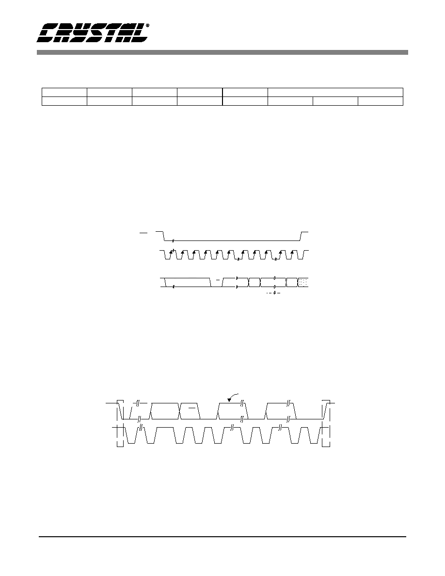
CS43L42
DS481PP2
31
7.3 Memory Address Pointer (MAP)
7.3.1 INCR (AUTO MAP INCREMENT ENABLE)
Default = `0'
0 - Disabled
1 - Enabled
7.3.2 MAP0-3 (MEMORY ADDRESS POINTER)
Default = `0000'
7
6
5
4
3
2
1
0
INCR
Reserved
Reserved
Reserved
MAP3
MAP2
MAP1
MAP0
0
0
0
0
0
0
0
0
M A P
MSB
L S B
DATA
b yte 1
byte n
R/W
M A P = M e m o ry A d d re s s P o in te r
ADDRESS
C H IP
C D IN
C C L K
CS
0 0 1 0 0 0 0
Figure 7. Control Port Timing, SPI mode
S D A
S C L
0 01 0 00
A D D R
A D 0
R /W
S ta rt
A C K
D A T A
1 -8
A C K
D A T A
1-8
A C K
Stop
N o te : If o p e ra tio n is a w rite , th is b yte co n ta in s th e M e m o ry A d d re ss P o in te r, M A P .
N o te 1
Figure 8. Control Port Timing, Two-Wire Mode

CS43L42
32
DS481PP2
Figure 9. Base-Rate Stopband Rejection
Figure 10. Base-Rate Transition Band
Figure 11. Base-Rate Transition Band (Detail)
Figure 12. Base-Rate Passband Ripple
-100
-90
-80
-70
-60
-50
-40
-30
-20
-10
0
0.0
0.1
0.2
0.3
0.4
0.5
0.6
0.7
0.8
0.9
1.0
Frequency (normalized to Fs)
Am
p
l
i
t
u
d
e
d
B
-100
-90
-80
-70
-60
-50
-40
-30
-20
-10
0
0.40
0.42
0.44
0.46
0.48
0.50
0.52
0.54
0.56
0.58
0.60
Frequency (normalized to Fs)
A
m
pl
i
t
u
de dB
Figure 13. High-Rate Stopband Rejection
Figure 14. High-Rate Transition Band

CS43L42
DS481PP2
33
-10
-9
-8
-7
-6
-5
-4
-3
-2
-1
0
0.45
0.46
0.47
0.48
0.49
0.50
0.51
0.52
0.53
0.54
0.55
Frequency (normalized to Fs)
Am
pl
i
t
ude dB
-0.30
-0.25
-0.20
-0.15
-0.10
-0.05
0.00
0.05
0.10
0.15
0.20
0.25
0.30
0.00
0.05
0.10
0.15
0.20
0.25
0.30
0.35
0.40
0.45
0.50
Frequency (normalized to Fs)
A
m
p
l
i
t
ude
d
B
Figure 15. High-Rate Transition Band (Detail)
Figure 16. High-Rate Passband Ripple
AOUTx
AGND
3.3 µF
V
out
R
L
C
L
+
Figure 17. Line Output Test Load
HP_x
AGND
220 µF
V
out
R
L
C
L
+
Figure 18. Headphone Output Test Load

CS43L42
34
DS481PP2
LR C K
S C L K
Le ft C ha n nel
R ig h t C ha n nel
S D A T A
+3 +2 +1 LSB
+5 +4
MSB -1 -2 -3 -4 -5
+3 +2 +1 LSB
+5 +4
M SB -1 -2 -3 -4
Internal SCLK Mode
External SCLK Mode
I
2
S, Up to 24-Bit data and INT SCLK = 64 Fs if
MCLK/LRCK = 512, 256 or 128
I
2
S, Up to 24-Bit data and INT SCLK = 48 Fs if
MCLK/LRCK = 384 or 192
I
2
S, up to 24-Bit Data
Data Valid on Rising Edge of SCLK
Figure 19. CS43L42 Control Port Mode - Serial Audio Format 0
Figure 20. CS43L42 Control Port Mode - Serial Audio Format 1
L R C K
S C L K
L e ft C h a n n e l
R ig h t C h a n n e l
S D A T A
+3 +2 +1 LSB
+5 +4
MSB -1 -2 -3 -4 -5
+3 +2 +1 LSB
+5 +4
MSB -1 -2 -3 -4
Internal SCLK Mode
External SCLK Mode
I
2
S, 16-Bit data and INT SCLK = 32 Fs if
MCLK/LRCK = 512, 256 or 128
I
2
S, Up to 24-Bit data and INT SCLK = 48 Fs if
MCLK/LRCK = 384 or 192
I
2
S, up to 24-Bit Data
Data Valid on Rising Edge of SCLK
Figure 21. CS43L42 Control Port Mode - Serial Audio Format 2
L R C K
S C L K
L e ft C h a n n e l
R ig h t C h a n n e l
S D A T A
+3 +2 +1 LS B
+5 +4
M SB -1 -2 -3 -4 -5
+3 +2 +1 LS B
+5 +4
M S B -1 -2 -3 -4
Internal SCLK Mode
External SCLK Mode
Left Justified, up to 24-Bit Data
INT SCLK = 64 Fs if MCLK/LRCK = 512, 256 or 128
INT SCLK = 48 Fs if MCLK/LRCK = 384 or 192
Left Justified, up to 24-Bit Data
Data Valid on Rising Edge of SCLK

CS43L42
DS481PP2
35
Figure 22. CS43L42 Control Port Mode - Serial Audio Format 3
LRCK
SCLK
L e ft C h a n n e l
SDATA
6
5
4
3
2
1
0
7
23 22 21 20 19 18
6
5
4
3
2
1
0
7
23 22 21 20 19 18
3 2 c lo cks
0
R ig h t C h a n n e l
Internal SCLK Mode
External SCLK Mode
Right Justified, 24-Bit Data
INT SCLK = 64 Fs if MCLK/LRCK = 512, 256 or 128
INT SCLK = 48 Fs if MCLK/LRCK = 384 or 192
Right Justified, 24-Bit Data
Data Valid on Rising Edge of SCLK
SCLK Must Have at Least 48 Cycles per LRCK Period
Figure 23. CS43L42 Control Port Mode - Serial Audio Format 4
L R C K
S C L K
L e ft C h a n n e l
R ig h t C h a n n e l
S D A T A
6
5
4
3
2
1
0
9
8
7
15 14 13 12 11 10
1
0
6
5
4
3
2
1
0
9
8
7
15 14 13 12 11 10
17 16
17 16
32 clocks
19 18
19 18
Internal SCLK Mode
External SCLK Mode
Right Justified, 20-Bit Data
INT SCLK = 64 Fs if MCLK/LRCK = 512, 256 or 128
INT SCLK = 48 Fs if MCLK/LRCK = 384 or 192
Right Justified, 20-Bit Data
Data Valid on Rising Edge of SCLK
SCLK Must Have at Least 40 Cycles per LRCK Period
Figure 24. CS43L42 Control Port Mode - Serial Audio Format 5
LRCK
SCLK
L e ft C h a n n e l
R ig h t C h a n n e l
SDATA
6
5
4
3
2
1
0
9
8
7
15 14 13 12 11 10
6
5
4
3
2
1
0
9
8
7
15 14 13 12 11 10
3 2 c lo cks
Internal SCLK Mode
External SCLK Mode
Right Justified, 16-Bit Data
INT SCLK = 32 Fs if MCLK/LRCK = 512, 256 or 128
INT SCLK = 48 Fs if MCLK/LRCK = 384 or 192
Right Justified, 16-Bit Data
Data Valid on Rising Edge of SCLK
SCLK Must Have at Least 32 Cycles per LRCK Period

CS43L42
36
DS481PP2
Figure 25. CS43L42 Control Port Mode - Serial Audio Format 6
L R C K
S C L K
L e ft C h a n n e l
R ig h t C h an n e l
S D A T A
6
5
4
3
2
1
0
9
8
7
15 14 13 12 11 10
1
0
6
5
4
3
2
1
0
9
8
7
15 14 13 12 11 10
17 16
17 16
32 clocks
Internal SCLK Mode
External SCLK Mode
Right Justified, 18-Bit Data
INT SCLK = 64 Fs if MCLK/LRCK = 512, 256 or 128
INT SCLK = 48 Fs if MCLK/LRCK = 384 or 192
Right Justified, 18-Bit Data
Data Valid on Rising Edge of SCLK
SCLK Must Have at Least 36 Cycles per LRCK Period
LR C K
S C L K
Le ft C ha n nel
R ig h t C ha n nel
S D A T A
+3 +2 +1 LSB
+5 +4
MSB -1 -2 -3 -4 -5
+3 +2 +1 LSB
+5 +4
M SB -1 -2 -3 -4
Internal SCLK Mode
External SCLK Mode
I
2
S, Up to 24-Bit data and INT SCLK = 64 Fs if
MCLK/LRCK = 512, 256 or 128
I
2
S, Up to 24-Bit data and INT SCLK = 48 Fs if
MCLK/LRCK = 384 or 192
I
2
S, up to 24-Bit Data
Data Valid on Rising Edge of SCLK
Figure 26. CS43L42 Stand Alone Mode - Serial Audio Format 0
Figure 27. CS43L42 Stand Alone Mode - Serial Audio Format 1
L R C K
S C L K
L e ft C h a n n e l
R ig h t C h a n n e l
S D A T A
+3 +2 +1 LS B
+5 +4
M SB -1 -2 -3 -4 -5
+3 +2 +1 LS B
+5 +4
M S B -1 -2 -3 -4
Internal SCLK Mode
External SCLK Mode
Left Justified, up to 24-Bit Data
INT SCLK = 64 Fs if MCLK/LRCK = 512, 256 or 128
INT SCLK = 48 Fs if MCLK/LRCK = 384 or 192
Left Justified, up to 24-Bit Data
Data Valid on Rising Edge of SCLK

CS43L42
DS481PP2
37
Figure 28. CS43L42 Stand Alone Mode - Serial Audio Format 2
LRCK
SCLK
L e ft C h a n ne l
SDATA
6
5
4
3
2
1
0
7
23 22 21 20 19 18
6
5
4
3
2
1
0
7
23 22 21 20 19 18
3 2 c lo cks
0
R ig h t C h a n n e l
Internal SCLK Mode
External SCLK Mode
Right Justified, 24-Bit Data
INT SCLK = 64 Fs if MCLK/LRCK = 512, 256 or 128
INT SCLK = 48 Fs if MCLK/LRCK = 384 or 192
Right Justified, 24-Bit Data
Data Valid on Rising Edge of SCLK
SCLK Must Have at Least 48 Cycles per LRCK Period
Figure 29. CS43L42 Stand Alone Mode - Serial Audio Format 3
LRCK
SCLK
L e ft C h a n ne l
R ig h t C h a n n e l
SDATA
6
5
4
3
2
1
0
9
8
7
15 14 13 12 11 10
6
5
4
3
2
1
0
9
8
7
15 14 13 12 11 10
3 2 c lo cks
Internal SCLK Mode
External SCLK Mode
Right Justified, 16-Bit Data
INT SCLK = 32 Fs if MCLK/LRCK = 512, 256 or 128
INT SCLK = 48 Fs if MCLK/LRCK = 384 or 192
Right Justified, 16-Bit Data
Data Valid on Rising Edge of SCLK
SCLK Must Have at Least 32 Cycles per LRCK Period

CS43L42
38
DS481PP2
Gain
dB
-10dB
0dB
Frequency
T2 = 15 µs
T1=50 µs
F1
F2
3.183 kHz
10.61 kHz
Figure 30. De-Emphasis Curve
Volume
Control
AoutA/HP_A
AoutB/HP_B
Left Channel
Audio Data
Right Channel
Audio Data
Volume
Control
MUTE
MUTE
EQ
EQ
Digital
A Channel
Digital
B Channel
Figure 31. ATAPI Block Diagram

CS43L42
DS481PP2
39
8. PARAMETER DEFINITIONS
Total Harmonic Distortion + Noise (THD+N)
The ratio of the rms value of the signal to the rms sum of all other spectral components over the specified
bandwidth (typically 10 Hz to 20 kHz), including distortion components. Expressed in decibels.
Dynamic Range
The ratio of the full scale rms value of the signal to the rms sum of all other spectral components over the
specified bandwidth. Dynamic range is a signal-to-noise measurement over the specified bandwidth
made with a -60 dBFS signal. 60 dB is then added to the resulting measurement to refer the measurement
to full scale. This technique ensures that the distortion components are below the noise level and do not
effect the measurement. This measurement technique has been accepted by the Audio Engineering So-
ciety, AES17-1991, and the Electronic Industries Association of Japan, EIAJ CP-307.
Interchannel Isolation
A measure of crosstalk between the left and right channels. Measured for each channel at the converter's
output with all zeros to the input under test and a full-scale signal applied to the other channel. Units in
decibels.
Interchannel Gain Mismatch
The gain difference between left and right channels. Units in decibels.
Gain Error
The deviation from the nominal full scale analog output for a full scale digital input.
Gain Drift
The change in gain value with temperature. Units in ppm/∞C.
9. REFERENCES
1) "How to Achieve Optimum Performance from Delta-Sigma A/D & D/A Converters" by Steven Harris.
Paper presented at the 93rd Convention of the Audio Engineering Society, October 1992.
2) CDB43L42 Evaluation Board Datasheet
3) "The I
2
C-Bus Specification: Version 2.0" Philips Semiconductors, December 1998.
http://www.semiconductors.philips.com

CS43L42
40
DS481PP2
10. PACKAGE DIMENSIONS
Notes: 1. "D" and "E1" are reference datums and do not included mold flash or protrusions, but do include mold
mismatch and are measured at the parting line, mold flash or protrusions shall not exceed 0.20 mm per
side.
2. Dimension "b" does not include dambar protrusion/intrusion. Allowable dambar protrusion shall be
0.13 mm total in excess of "b" dimension at maximum material condition. Dambar intrusion shall not
reduce dimension "b" by more than 0.07 mm at least material condition.
3. These dimensions apply to the flat section of the lead between 0.10 and 0.25 mm from lead tips.
INCHES
MILLIMETERS
NOTE
DIM
MIN
NOM
MAX
MIN
NOM
MAX
A
--
--
0.043
--
--
1.10
A1
0.002
0.004
0.006
0.05
--
0.15
A2
0.03346
0.0354
0.037
0.85
0.90
0.95
b
0.00748
0.0096
0.012
0.19
0.245
0.30
2,3
D
0.303
0.307
0.311
7.70
7.80
7.90
1
E
0.248
0.2519
0.256
6.30
6.40
6.50
E1
0.169
0.1732
0.177
4.30
4.40
4.50
1
e
--
0.026 BSC
--
--
0.65 BSC
--
L
0.020
0.024
0.028
0.50
0.60
0.70
0∞
4∞
8∞
0∞
4∞
8∞
JEDEC #: MO-153
Controlling Dimension is Millimeters.
24L TSSOP (4.4 mm BODY) PACKAGE DRAWING
E
N
1 2 3
e
b
2
A1
A2
A
D
SEATING
PLANE
E1
1
L
SIDE VIEW
END VIEW
TOP VIEW