
Copyright
© Cirrus Logic, Inc. 2004
(All Rights Reserved)
http://www.cirrus.com
Preliminary Product Information
This document contains information for a new product.
Cirrus Logic reserves the right to modify this product without notice.
Features
16-Pin TSSOP Package
1.8 to 3.3 Volt Supply
24-Bit Conversion / 96 kHz Sample Rate
94 dB Dynamic Range at 3 V Supply
-85 dB THD+N at 1.8 V Supply
Low Power Consumption
Digital Volume Control
∑ 96 dB Attenuation, 1 dB Step Size
Digital Bass and Treble Boost
∑ Selectable Corner Frequencies
∑ Up to 12 dB Boost in 1 dB Increments
Peak Signal Limiting to Prevent Clipping
De-emphasis for 32 kHz, 44.1 kHz, and
48 kHz
Headphone Amplifier
∑ up to 22 mW
rms
Power Output into 16
Load*
∑ 25 dB Analog Attenuation and Mute
∑ Zero Crossing Click-free Level Transitions
ATAPI Mixing Functions
Description
The CS43L43 is a complete stereo digital-to-analog out-
put system including interpolation, 1-bit D/A conversion,
analog filtering, volume control, and a headphone ampli-
fier, in a 16-pin TSSOP package.
The CS43L43 is based on delta-sigma modulation,
where the modulator output controls the reference volt-
age input to an ultra-linear analog low-pass filter. This
architecture allows infinite adjustment of the sample rate
between 2 kHz and 100 kHz simply by changing the
master clock frequency.
The CS43L43 contains on-chip digital bass and treble
boost, peak signal limiting and de-emphasis. The
CS43L43 operates from a +1.8 V to +3.3 V supply and
consumes only 16 mW of power with a 1.8 V supply.
These features are ideal for portable CD, MP3 and MD
players and other portable playback systems that require
extremely low power consumption.
ORDERING INFORMATION
CS43L43-KZ
-10 to 70 ∞C
16-pin TSSOP
CS43L43-KZZ, Lead Free -10 to 70 ∞C
16-pin TSSOP
CDB43L43
Evaluation Board
* 1 kHz sine wave at 3.3V supply
SCLK/DEM
SDATA
DIF1/SDA
MCLK
HP_A
SERIAL
AUDIO
DE-
CONTROL PORT INTERFACE
DAC
RST
LRCK
DIF0/SCL
DIGITAL
VOLUME
CONTROL
DAC
DIGITAL
ANALOG
FILTER
ANALOG
FILTER
ANALOG
VOLUME
CONTROL
HEAD-
PHONE
AMPLIFIER
ANALOG
VOLUME
CONTROL
HP_B
EMPHASIS
BASS/TREBLE
BOOST
LIMITING
INTERFACE
FILTER
CS43L43
Low Voltage, Stereo DAC with Headphone Amp
JUL `04
DS479PP3

CS43L43
2
DS479PP3
TABLE OF CONTENTS
1.0 PIN DESCRIPTION ..............................................................................................4
2.0 TYPICAL CONNECTION DIAGRAM .................................................................5
3.0 APPLICATIONS ...................................................................................................6
3.1 Sample Rate Range/Operational Mode Select ...........................................6
3.2 System Clocking .........................................................................................6
3.3 Digital Interface Format ..............................................................................7
3.4 De-Emphasis Control ..................................................................................8
3.5 Recommended Power-up Sequence ..........................................................9
3.6 Popguard
Æ
Transient Control .....................................................................9
3.7 Grounding and Power Supply Arrangements ...........................................12
3.8 Control Port Interface ................................................................................12
3.9 Memory Address Pointer (MAP) ...............................................................14
4.0 REGISTER QUICK REFERENCE .....................................................................14
5.0 REGISTER DESCRIPTION ...............................................................................15
5.1 Power and Muting Control (address 01h) .................................................15
5.2 Channel A Analog Attenuation Control (address 02h) (VOLA).................17
5.3 Channel B Analog Attenuation Control (address 03h) (VOLB).................17
5.4 Channel A Digital Volume Control (address 04h) (DVOLA) ......................18
5.5 Channel B Digital Volume Control (address 05h) (DVOLB) ......................18
5.6 Tone Control (address 06h).......................................................................18
5.7 Mode Control (address 07h) ......................................................................19
5.8 Limiter Attack Rate (address 08h) (ARATE)..............................................21
5.9 Limiter Release Rate (address 09h) (RRATE) ......................................21
5.10 Volume and Mixing Control (address 0Ah) ..............................................22
5.11 Mode Control 2 (address 0Bh).................................................................24
6.0 CHARACTERISTICS AND SPECIFICATIONS .................................................25
ANALOG CHARACTERISTICS (CS43L43-KZ)................................................25
COMBINED INTERPOLATION & ON-CHIP ANALOG FILTER RESPONSE ..27
SWITCHING SPECIFICATIONS - SERIAL AUDIO INTERFACE ....................30
Contacting Cirrus Logic Support
For a complete listing of Direct Sales, Distributor, and Sales Representative contacts, visit the Cirrus Logic web site at:
http://www.cirrus.com/corporate/contacts
IMPORTANT NOTICE
"Preliminary" product information describes products that are in production, but for which full characterization data is not yet available. "Advance" product informa-
tion describes products that are in development and subject to development changes. Cirrus Logic, Inc. and its subsidiaries ("Cirrus") believe that the information
contained in this document is accurate and reliable. However, the information is subject to change without notice and is provided "AS IS" without warranty of any
kind (express or implied). Customers are advised to obtain the latest version of relevant information to verify, before placing orders, that information being relied
on is current and complete. All products are sold subject to the terms and conditions of sale supplied at the time of order acknowledgment, including those pertaining
to warranty, patent infringement, and limitation of liability. No responsibility is assumed by Cirrus for the use of this information, including use of this information as
the basis for manufacture or sale of any items, or for infringement of patents or other rights of third parties. This document is the property of Cirrus and by furnishing
this information, Cirrus grants no license, express or implied under any patents, mask work rights, copyrights, trademarks, trade secrets or other intellectual property
rights. Cirrus owns the copyrights of the information contained herein and gives consent for copies to be made of the information only for use within your organization
with respect to Cirrus integrated circuits or other parts of Cirrus. This consent does not extend to other copying such as copying for general distribution, advertising
or promotional purposes, or for creating any work for resale.
An export permit needs to be obtained from the competent authorities of the Japanese Government if any of the products or technologies described in this material
and controlled under the "Foreign Exchange and Foreign Trade Law" is to be exported or taken out of Japan. An export license and/or quota needs to be obtained
from the competent authorities of the Chinese Government if any of the products or technologies described in this material is subject to the PRC Foreign Trade Law
and is to be exported or taken out of the PRC.
CERTAIN APPLICATIONS USING SEMICONDUCTOR PRODUCTS MAY INVOLVE POTENTIAL RISKS OF DEATH, PERSONAL INJURY, OR SEVERE PROP-
ERTY OR ENVIRONMENTAL DAMAGE ("CRITICAL APPLICATIONS"). CIRRUS PRODUCTS ARE NOT DESIGNED, AUTHORIZED, OR WARRANTED TO BE
SUITABLE FOR USE IN LIFE-SUPPORT DEVICES OR SYSTEMS OR OTHER CRITICAL APPLICATIONS. INCLUSION OF CIRRUS PRODUCTS IN SUCH
APPLICATIONS IS UNDERSTOOD TO BE FULLY AT THE CUSTOMER'S RISK.
Purchase of I
2
C components of Cirrus Logic, Inc., or one of its sublicensed Associated Companies conveys a license under the Phillips I
2
C Patent Rights to use
those components in a standard I
2
C system.
Cirrus Logic, Cirrus, and the Cirrus Logic logo designs are trademarks of Cirrus Logic, Inc. All other brand and product names in this document may be trademarks
or service marks of their respective owners.

CS43L43
DS479PP3
3
SWITCHING CHARACTERISTICS - INTERNAL SERIAL CLOCK.................. 31
SWITCHING SPECIFICATIONS - CONTROL PORT INTERFACE................. 32
DC ELECTRICAL CHARACTERISTICS .......................................................... 33
DIGITAL INPUT CHARACTERISTICS & SPECIFICATIONS .......................... 33
THERMAL CHARACTERISTICS AND SPECIFICATIONS.............................. 33
RECOMMENDED OPERATING SPECIFICATIONS .......................................34
ABSOLUTE MAXIMUM RATINGS................................................................... 34
7.0 PARAMETER DEFINITIONS ............................................................................. 35
8.0 REFERENCES ................................................................................................... 35
9.0 PACKAGE DIMENSIONS .................................................................................36
LIST OF FIGURES
Figure 1. Typical Connection Diagram .............................................................................. 5
Figure 2. I
2
S Data .............................................................................................................. 8
Figure 3. Left Justified up to 24-Bit Data ........................................................................... 8
Figure 4. Right Justified Data ............................................................................................ 8
Figure 5. De-Emphasis Curve ........................................................................................... 8
Figure 6. Optional Headphone Mute Circuit .................................................................... 11
Figure 7. Timing for Headphone Mute ............................................................................. 11
Figure 8. Control Port Timing .......................................................................................... 13
Figure 9. ATAPI Block Diagram ....................................................................................... 23
Figure 10. Output Test Load ............................................................................................ 26
Figure 11. Single-Speed Stopband Rejection ................................................................. 28
Figure 12. Single-Speed Transition Band ........................................................................ 28
Figure 13. Single-Speed Transition Band (Detail) ........................................................... 28
Figure 14. Single-Speed Passband Ripple ...................................................................... 28
Figure 15. Double-Speed Stopband Rejection ................................................................ 28
Figure 16. Double-Speed Transition Band ...................................................................... 28
Figure 17. Double-Speed Transition Band (Detail) .......................................................... 29
Figure 18. Double-Speed Passband Ripple .................................................................... 29
Figure 19. External Serial Mode Input Timing ................................................................. 30
Figure 20. Internal Serial Mode Input Timing .................................................................. 31
Figure 21. Internal Serial Clock Generation .................................................................... 31
Figure 22. Control Port Timing - I2C Mode ..................................................................... 32
LIST OF TABLES
Table 1. CS43L43 Operational Mode ................................................................................ 6
Table 2. Single-Speed Mode Standard Frequencies ......................................................... 6
Table 3. Double-Speed Mode Standard Frequencies ....................................................... 6
Table 4. Internal SCLK/LRCK Ratio .................................................................................. 7
Table 5. Digital Interface Format - Stand-Alone Mode ......................................................7
Table 6. De-Emphasis Control .......................................................................................... 9
Table 7. Example Analog Volume Settings ..................................................................... 17
Table 8. Example Digital Volume Settings ...................................................................... 18
Table 9. Example Bass Boost Settings ........................................................................... 18
Table 10. Example Treble Boost Settings ....................................................................... 19
Table 11. Example Limiter Attack Rate Settings ............................................................. 21
Table 12. Example Limiter Release Rate Settings .......................................................... 21
Table 13. ATAPI Decode ................................................................................................. 23
Table 14. Digital Interface Format - Control Port Mode ................................................... 24

CS43L43
4
DS479PP3
1.0 PIN DESCRIPTION
Pin Name
#
Pin Description
LRCK
1
Left Right Clock (Input) - Determines which channel, Left or Right, is currently active on the
serial audio data line.
SDATA
2
Serial Audio Data (Input) - Input for two's complement serial audio data.
SCLK
3
Serial Clock (Input) - Serial clock for the serial audio interface.
DEM
3
De-emphasis Control (Input) - Selects the standard 15
µs/50µs digital de-emphasis filter
response for 44.1 kHz sample rates.
VL
4
Logic Power (Input) - Positive power for the serial audio & control port interface.
MCLK
5
Master Clock (Input) - Clock source for the delta-sigma modulator and digital filters.
VQ_HP
7
Headphone Quiescent Voltage (Output) - Filter connection for internal headphone amp quies-
cent reference voltage.
REF_GND
8
Reference Ground (Input) - Ground reference for the internal sampling circuits.
FILT+
9
Positive Voltage Reference (Output) - Positive voltage reference for the internal sampling cir-
cuits.
HP_A
HP_B
10
14
Headphone Outputs (Output) - The full-scale analog headphone output level is specified in the
Analog Characteristics table.
GND
11
Ground (Input) - Ground reference.
VA
12
Power (Input) - Positive power for the analog & digital sections.
VA_HP
13
Headphone Amp Power (Input) - Positive power for the headphone amplifier.
RST
16
Reset (Input) - Powers down device and resets registers to default conditions when enabled.
Stand-Alone
Definitions
DIF0
DIF1
6
15
Digital Interface Format (Input) - Defines the required relationship between the Left Right
Clock, Serial Clock, and Serial Audio Data.
Control Port
Definitions
SCL
6
Serial Control Port Clock (Input) - Serial clock for the control port interface.
SDA 15
Serial Control Data I/O (Input/Output) - Input/Output for I
2
C data.
LRCK
RST
SDATA
DIF1/SDA
SCLK/DEM
HP_B
VL
VA_HP
MCLK
VA
DIF0/SCL
GND
VQ_HP
HP_A
REF_GND
FILT+
1
2
3
4
5
6
7
8
5
1
2
6
16
15
14
13
12
11
10
9
1
2
3
4
5
6
7
8
5
1
2
6
16
15
14
13
12
11
10
9

CS43L43
DS479PP3
5
2.0 TYPICAL CONNECTION DIAGRAM
MCLK
LRCK
SCLK/DEM
SDATA
RST
DIF0/SCL
DIF1/SDA
GND
µc/
Serial Audio
Data
Processor
VA
VA_HP
HP_A
HP_B
FILT+
CS43L43
0.1 µF
0.1 µF
1.0 µF
220 µF
220 µF
1.8 to 3.3 V
Supply
*1.0 µF
0.1 µF
+
VL
*Ferrite
bead
+
+
+
12
13
4
5
1
3
2
10
14
16
6
15
8
9
7
11
1 k
1 k
µH
47 µH
*
Optional
Mode
Configuration
+
16
Headphones
1.0 µF
VQ_HP
REF_GND
47
1.8 to 3.3 V
Supply
*Ferrite
bead
*1.0 µF
+
+
*Ferrite
bead
*1.0 µF
0.9 to 3.3 V
Supply
Figure 1. Typical Connection Diagram
CS43L43
6
DS479PP3
3.0 APPLICATIONS
3.1 Sample Rate Range/Operational Mode Select
The device operates in one of two operational modes. Operation in either mode depends on the input sam-
ple rate and the ratio of the master clock to the left/right clock (see section 3.2). Sample rates outside the
specified range for each mode are not supported.
3.2 System Clocking
The device requires external generation of the master (MCLK) and left/right (LRCK) clocks. The device
also requires external generation of the serial clock (SCLK) if the internal serial clock is not used. The
LRCK, defined also as the input sample rate F
s
, must be synchronously derived from MCLK according to
specified ratios. The specified ratios of MCLK to LRCK, along with several standard audio sample rates
and the required MCLK frequency, are illustrated in Tables 2-3.
*Requires MCLKDIV bit = 1 in the Mode Control 2 register (address 0Bh).
Input Sample Rate (F
S
)
MODE
2kHz - 50kHz
Single Speed Mode
50kHz - 100kHz
Double Speed Mode
Table 1. CS43L43 Operational Mode
Sample Rate
(kHz)
MCLK (MHz)
256x
384x
512x
768x*
1024x*
32
8.1920
12.2880
16.3840
24.5760
32.768
44.1
11.2896
16.9344
22.5792
33.8688
45.1584
48
12.2880
18.4320
24.5760
36.8640
49.1520
Table 2. Single-Speed Mode Standard Frequencies
Sample Rate
(kHz)
MCLK (MHz)
128x
192x
256x*
384x*
64
8.1920
12.2880
16.3840
24.5760
88.2
11.2896
16.9344
22.5792
33.8688
96
12.2880
18.4320
24.5760
36.8640
Table 3. Double-Speed Mode Standard Frequencies

CS43L43
DS479PP3
7
3.2.1 Internal Serial Clock Mode
The device will enter the Internal Serial Clock Mode if no low to high transitions are detected on the
SCLK pin for 2 consecutive periods of LRCK. In this mode, the SCLK is internally derived and syn-
chronous with MCLK and LRCK. The SCLK/LRCK ratio is either 32, 48, or 64 depending upon the
MCLK/LRCK ratio and the Digital Interface Format selection (see Table 4).
The internal serial clock is utilized when de-emphasis control is required. Operation in the Internal
Serial Clock mode is identical to operation with an external SCLK synchronized with LRCK; how-
ever, External SCLK mode is the recommended system clocking application.
3.2.2 External Serial Clock Mode
The device will enter the External Serial Clock Mode whenever 16 low to high transitions are detect-
ed on the SCLK pin during any phase of the LRCK period. The device will revert to Internal Serial
Clock Mode if no low to high transitions are detected on the SCLK pin for 2 consecutive periods of
LRCK.
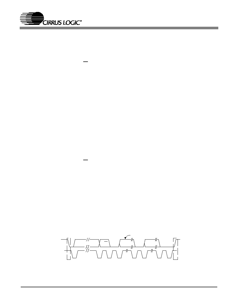
3.3 Digital Interface Format
The device will accept audio samples in 1 of 4 digital interface formats in Stand-Alone mode, as illustrated
in Table 5, and 1 of 7 formats in Control Port mode, as illustrated in Table 14.
3.3.1 Stand-Alone Mode
The desired format is selected via the DIF0 and DIF1 pins. For an illustration of the required rela-
tionship between the LRCK, SCLK and SDATA, see Figures 2-4.
Input
Digital Interface Format Selection
Internal
MCLK/LRCK
Ratio
I
2
S up to 24
Bits
I
2
S 16
Bits
Left Justified 24
Bits
Right Justified
24, 20, or 18 Bits
Right Justified
16 Bits
SCLK/LRCK
Ratio
512, 256, 128
X
X
32
384, 192
X
X
X
X
48
512, 256, 128
X
X
X
64
Table 4. Internal SCLK/LRCK Ratio
DIF1
DIF0
DESCRIPTION
FORMAT
FIGURE
0
0
I
2
S, up to 24-bit data
0
2
0
1
Left Justified, up to 24-bit data
1
3
1
0
Right Justified, 24-bit Data
2
4
1
1
Right Justified, 16-bit Data
3
4
Table 5. Digital Interface Format - Stand-Alone Mode

CS43L43
8
DS479PP3
3.3.2
Control Port Mode
The desired format is selected via the DIF0, DIF1 and DIF2 bits in the Mode Control 2 register (see
section 5.11.2) . For an illustration of the required relationship between LRCK, SCLK and SDATA,
see Figures 2-4.
3.4 De-Emphasis Control
The device includes on-chip digital de-emphasis. Figure 5 shows the de-emphasis curve for F
s
equal to
44.1 kHz. The frequency response of the de-emphasis curve will scale proportionally with changes in sam-
ple rate, Fs. De-emphasis is not available in double-speed mode.
L R C K
S C L K
L e ft C h a n n e l
R ig h t C h a n n e l
S D A T A
+ 3 + 2 + 1
+ 5 + 4
M S B
-1 -2 -3 -4 -5
+ 3 + 2 + 1
+ 5 + 4
-1 -2 -3 -4
M S B
L S B
L S B
Figure 2. I
2
S Data
L R C K
S C L K
L e ft C h a n n e l
R ig h t C h a n n e l
S D A T A
+ 3 + 2 + 1
+ 5 + 4
M S B
-1 -2 -3 -4 -5
+ 3 + 2 + 1
+ 5 + 4
-1 -2 -3 -4
L S B
M S B
L S B
Figure 3. Left Justified up to 24-Bit Data
LR C K
S C LK
L e ft C h a n n e l
S D A T A
-6 -5 -4 -3 -2 -1
-7
+1 + 2 +3 + 4 +5
3 2 c lo ck s
M S B
R ig h t C h a n n e l
L S B
M S B
+1 + 2 +3 + 4 +5
L S B
-6 -5 -4 -3 -2 -1
-7
M S B
Figure 4. Right Justified Data
Gain
dB
-10dB
0dB
Frequency
T2 = 15 µs
T1=50 µs
F1
F2
3.183 kHz
10.61 kHz
Figure 5. De-Emphasis Curve

CS43L43
DS479PP3
9
3.4.1 Stand-Alone Mode
When using Internal Serial Clock (see section 3.2.1), pin 3 is available for de-emphasis control and
selects the 44.1 kHz de-emphasis filter. Please see Table 6 for the desired de-emphasis control.
Table 6. De-Emphasis Control
3.4.2 Control Port Mode
The Mode Control bits select either the 32, 44.1, or 48 kHz de-emphasis filter. Please see section
5.7.4 for the desired de-emphasis control.
3.5 Recommended Power-up Sequence
3.5.1 Stand-Alone Mode
1. Hold RST low until the power supply and configuration pins are stable, and the master and
left/right clocks are locked to the appropriate frequences, as discussed in section 3.2. In this state, the
control port is reset to its default settings and VQ_HP will remain low.
2. Bring RST high. The device will remain in a low power state with VQ_HP low and will initiate
the Stand-Alone power-up sequence after approximately 1024 LRCK cycles.
3.5.2 Control Port Mode
1. Hold RST low until the power supply is stable, and the master and left/right clocks are locked to
the appropriate frequences, as discussed in section 3.2. In this state, the control port is reset to its de-
fault settings and VQ_HP will remain low.
2. Bring RST high. The device will remain in a low power state with VQ_HP low. The control port
will be accessible at this time.
3. Wait approximately 2 LRCK cycles and then perform an I
2
C write to the CP_EN bit prior to the
completion of approximately 1024 LRCK cycles. The desired register settings can be loaded while
keeping the PDN bit set to 1.
4. Set the PDN bit to 0. This will initiate the power-up sequence, which lasts approximately 50 µS
when the POR bit is set to 0. If the POR bit is set to 1, see Section 3.6 for for a complete description
of power-up timing.
3.6 Popguard
Æ
Transient Control
The CS43L43 uses Popguard
Æ
technology to minimize the effects of output transients during power-up
and power-down. This technology, when used with external DC-blocking capacitors in series with the au-
dio outputs, minimizes the audio transients commonly produced by single-ended single-supply converters.
It is activated inside the DAC when the RST pin is enabled/disabled and requires no other external control,
aside from choosing the appropriate DC-blocking capacitors.
DEM
DESCRIPTION
0
Disabled
1
44.1 kHz

CS43L43
10
DS479PP3
3.6.1 Power-up
When the device is initially powered-up, the audio outputs, HP_A and HP_B, are clamped to GND.
Following a delay of approximately 1000 sample periods, each output begins to ramp toward the qui-
escent voltage. Approximately 10,000 LRCK cycles later, the outputs reach V
Q
and audio output be-
gins. This gradual voltage ramping allows time for the external DC-blocking capacitors to charge to
the quiescent voltage, minimizing the power-up transient.
3.6.2 Power-down
To prevent transients at power-down, the device must first enter its power-down state by setting the
RST pin low. When this occurs, audio output ceases and the internal output buffers are disconnected
from HP_A and HP_B. In their place, a soft-start current sink is substituted which allows the
DC-blocking capacitors to slowly discharge. Once this charge is dissipated, the power to the device
may be turned off and the system is ready for the next power-on.
3.6.3 Discharge Time
To prevent an audio transient at the next power-on, the DC-blocking capacitors must fully discharge
before turning on the power or exiting the power-down state. If full discharge does not occur, a tran-
sient will occur when the audio outputs are initially clamped to GND. The time that the device must
remain in the power-down state is related to the value of the DC-blocking capacitance and the output
load. For example, with a 220 µF capacitor and a 16
load, the minimum power-down time will be
approximately 0.4 seconds.

CS43L43
DS479PP3
11
3.6.4 Auxilliary Mute Control
For critical applications, the Popguard
Æ
Transient Control may not be sufficient in eliminating extra-
neous audible artifacts on the headphone outputs during power-up. For these applications, an option-
al external mute can be used to maintain an absolute minimum of extraneous clicks and pops. Please
see Figures 6 and 7 for the suggested headphone mute circuit.
The Mute Control will need to be generated externally from a DSP or Microcontroller. See Figure 7
for /RST and Mute Control timing.
H eadphones
T he M otorola M O SFET s show n have been
tested to w ork properly, how ever, an
equivalent device m ay be used.
M G S F1N H 02E LT
2 2 0uF
47u H
1k
16
100K
M G S F1N H 02E LT
2 2 0uF
47u H
1k
16
From C S 43L43 P in
1 4 (H P _B )
From C S 43L43 P in
1 0 (H P _A )
M ute C ontrol from uC or D S P
Figure 6. Optional Headphone Mute Circuit
~ 3 0 0 m s e c
~ 9 0 0 m s e c
H eadphone O utput at
pin of part
/R S T
M ute C ontrol from
D S P or
M icroC ontroller
Figure 7. Timing for Headphone Mute

CS43L43
12
DS479PP3
3.7 Grounding and Power Supply Arrangements
As with any high resolution converter, the CS43L43 requires careful attention to power supply and ground-
ing arrangements if its potential performance is to be realized. Figure 1 shows the recommended power
arrangements, with VA, VA_HP & VL connected to clean supplies. If the ground planes are split between
digital ground and analog ground, the GND pins of the CS43L43 should be connected to the analog ground
plane.
All signals, especially clocks, should be kept away from the FILT+ and VQ pins in order to avoid unwant-
ed coupling into the modulators. The CDB43L43 evaluation board demonstrates the optimum layout and
power supply arrangements.
Notes: The headphone outputs may clip when the value of VA_HP is below VA. It is recommended that these two
supplies be tied together.
3.7.1 Capacitor Placement
Decoupling capacitors should be as close to the DAC as possible, with the low value ceramic capac-
itor being the closest. The FILT+ and VQ decoupling capacitors must be positioned to minimize the
electrical path from FILT+ to REF_GND (and VQ to REF_GND). To further minimze impedance,
these capacitors should be located on the same layer as the DAC.
3.8 Control Port Interface
The control port is used to load all the internal register settings. Data is clocked into and out of the bi-di-
rectional serial control data line, SDA, by the serial control port clock, SCL (see Figure 8 for the clock to
data relationship). The operation of the control port may be completely asynchronous with the audio sam-
ple rate. However, to avoid potential interference problems, the control port pins should remain static if no
operation is required.
Notes: LRCK & MCLK must always be applied to pins 1 & 5, respectively, during any communication with the
control port.
3.8.1 Enabling the Control Port
The control port pins are shared with the stand-alone configuration pins. To dedicate these pins to
control port functionality, enable the control port prior to the completion of the stand-alone power up
sequence (see section 3.5 for the Recommended Power-up Sequence). To enable the control port,
write 1 to the CP_EN bit using the I
2
C protocol (see section 3.8.3).
Notes: Setting the CP_EN bit after the Stand-Alone power-up sequence has completed can cause audible
artifacts.
3.8.2 MAP Auto Increment
The device has MAP (memory address pointer) auto increment capability enabled by the INCR bit
(also the MSB) of the MAP. If INCR is set to 0, MAP will stay constant for successive I
2
C writes or
reads. If INCR is set to 1, MAP will auto increment after each byte is written, allowing block reads
or writes of successive registers.
CS43L43
DS479PP3
13
3.8.3 I
2
C Write
To write to the device, follow the procedure below while adhering to the control port Switching Spec-
ifications in section 6.
1) Initiate a START condition to the I
2
C bus followed by the address byte, 00100000. The eighth bit
of the address byte is the R/W bit.
2) Wait for an acknowledge (ACK) from the part, then write to the memory address pointer, MAP.
This byte points to the register to be written.
3) Wait for an acknowledge (ACK) from the part, then write the desired data to the register pointed
to by the MAP.
4) If the INCR bit (see section 3.8.2) is set to 1, repeat the previous step until all the desired registers
are written, then initiate a STOP condition to the bus.
5) If the INCR bit is set to 0 and further I
2
C writes to other registers are desired, it is necessary to
initiate a repeated START condition and follow the procedure detailed from step 1. If no further
writes to other registers are desired, initiate a STOP condition to the bus.
3.8.4 I
2
C Read
To read from the device, follow the procedure below while adhering to the control port Switching
Specifications.
1) Initiate a START condition to the I
2
C bus followed by the address byte, 00100001. The eighth bit
of the address byte is the R/W bit.
2) After transmitting an acknowledge (ACK), the device will then transmit the contents of the regis-
ter pointed to by the MAP. The MAP will contain the address of the last register written to the MAP,
or the default address (see section 3.9) if an I
2
C read is the first operation performed on the device.
3) Once the device has transmitted the contents of the register pointed to by the MAP, issue an ACK.
4) If the INCR bit is set to 1, the device will continue to transmit the contents of successive registers.
Continue providing a clock and issue an ACK after each byte until all the desired registers are read,
then initiate a STOP condition to the bus.
5) If the INCR bit is set to 0 and further I
2
C reads from other registers are desired, it is necessary to
initiate a repeated START condition and follow the procedure detailed from step 1. If no further reads
from other registers are desired, initiate a STOP condition to the bus.
S D A
S C L
0 0 1 0 0 0
R /W
S ta r t
A C K
D A T A
1 - 8
A C K
D A T A
1 - 8
A C K
S to p
N O T E
0
N O T E : If o p e r a tio n is a w r ite , th is b y te c o n ta in s th e M e m o r y A d d r e s s P o in te r , M A P . If
o p e r a tio n is a r e a d , th is b y te c o n ta in s th e d a ta o f th e r e g is te r p o in te d to b y th e M A P .
Figure 8. Control Port Timing
CS43L43
14
DS479PP3
3.9 Memory Address Pointer (MAP)
3.9.1 INCR (Auto Map Increment Enable)
Default = `0'
0 - Disabled
1 - Enabled
3.9.2 MAP0-3 (Memory Address Pointer)
Default = `0000'
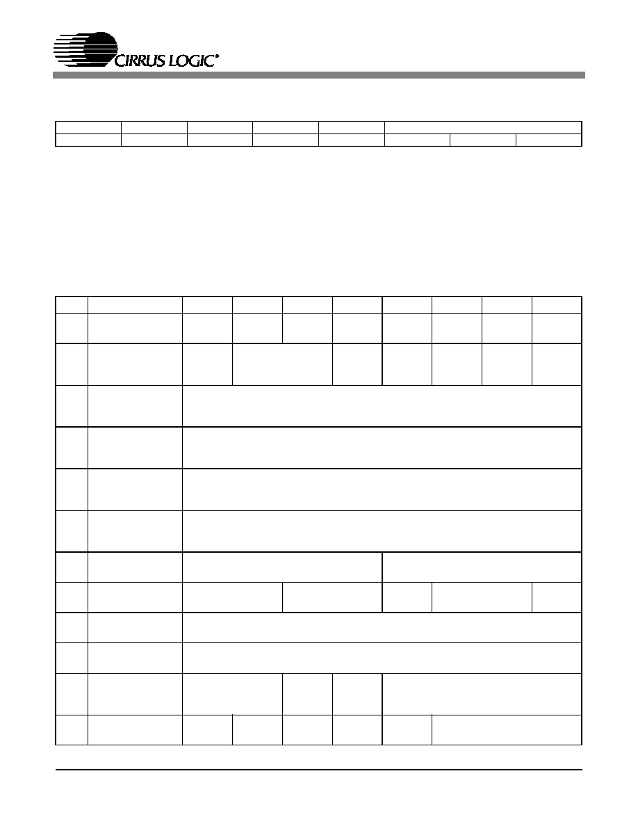
4.0 REGISTER QUICK REFERENCE
7
6
5
4
3
2
1
0
INCR
Reserved
Reserved
Reserved
MAP3
MAP2
MAP1
MAP0
0
0
0
0
0
0
0
0
Addr
Function
7
6
5
4
3
2
1
0
0h
Reserved
Reserved Reserved Reserved Reserved Reserved Reserved Reserved Reserved
default
0
0
0
0
0
0
0
0
1h
Power and Muting
Control
AMUTE
SZC1
SZC0
POR
Reserved Reserved
PDN
CP_EN
default
1
1
0
1
0
0
1
0
2h
Channel A Analog
Attenuation Control
VOLA7
VOLA6
VOLA5
VOLA4
VOLA3
VOLA2
VOLA1
VOLA0
default
0
0
0
0
0
0
0
0
3h
Channel B Analog
Attenuation Control
VOLB7
VOLB6
VOLB5
VOLB4
VOLB3
VOLB2
VOLB1
VOLB0
default
0
0
0
0
0
0
0
0
4h
Channel A Digital
Volume Control
DVOLA7
DVOLA6
DVOLA5
DVOLA4
DVOLA3
DVOLA2
DVOLA1
DVOLA0
default
0
0
0
0
0
0
0
0
5h
Channel B Digital
Volume Control
DVOLB7
DVOLB6
DVOLB5
DVOLB4
DVOLB3
DVOLB2
DVOLB1
DVOLB0
default
0
0
0
0
0
0
0
0
6h
Tone Control
BB3
BB2
BB1
BB0
TB3
TB2
TB1
TB0
default
0
0
0
0
0
0
0
0
7h
Mode Control
BBCF1
BBCF0
TBCF1
TBCF0
A=B
DEM1
DEM0
VCBYP
default
0
0
0
0
0
0
0
0
8h
Limiter Attack Rate
ARATE7
ARATE6
ARATE5
ARATE4
ARATE3
ARATE2
ARATE1
ARATE0
default
0
0
0
1
0
0
0
0
9h
Limiter Release Rate
RRATE7
RRATE6
RRATE5
RRATE4
RRATE3
RRATE2
RRATE1
RRATE0
default
0
0
1
0
0
0
0
0
Ah
Volume and Mixing
Control
TC1
TC0
TC_EN
LIM_EN
ATAPI3
ATAPI2
ATAPI1
ATAPI0
default
0
0
0
0
1
0
0
1
Bh
Mode Control 2
MCLKDIV Reserved Reserved Reserved Reserved
DIF2
DIF1
DIF0
default
0
0
0
0
0
0
0
0
CS43L43
DS479PP3
15
5.0 REGISTER DESCRIPTIONS
5.1 POWER AND MUTING CONTROL (ADDRESS 01H)
5.1.1 AUTO-MUTE (AMUTE)
BIT 7
Default = 1
0 - Disabled
1 - Enabled
Function:
The Digital-to-Analog converter output will mute following the reception of 8192 consecutive audio sam-
ples of static 0 or -1. A single sample of non-static data will release the mute. Detection and muting is
done independently for each channel. The quiescent voltage on the output will be retained. The muting
function is affected, similar to volume control changes, by the Soft and Zero Cross bits in the Power and
Muting Control register.
5.1.2 SOFT RAMP AND ZERO CROSS CONTROL (SZC)
BIT 5-6
Default = 10
00 - Immediate Change
01 - Zero Cross Digital and Analog
10 - Ramped Digital and Analog
11 - Reserved
Function:
Immediate Change
When Immediate Change is selected all level changes will take effect immediately in one step.
Zero Cross Digital and Analog
Zero Cross Enable dictates that signal level changes, either by attenuation changes or muting, will occur
on a signal zero crossing to minimize audible artifacts. The requested level change will occur after a
timeout period of 512 sample periods (10.7 ms at 48 kHz sample rate) if the signal does not encounter a
zero crossing. The zero cross function is independently monitored and implemented for each channel.
Ramped Digital and Analog
Soft Ramp allows digital level changes, both muting and attenuation, to be implemented by incrementally
ramping, in 1/8 dB steps, from the current level to the new level at a rate of 1dB per 8 left/right clock pe-
riods. Analog level changes will occur in 1 dB steps on a signal zero crossing. The analog level change
will occur after a timeout period of 512 sample periods (10.7 ms at 48 kHz sample rate) if the signal does
not encounter a zero crossing. The zero cross function is independently monitored and implemented for
each channel.
NOTE: Ramped Digital and Analog is not available in Double-Speed mode.
7
6
5
4
3
2
1
0
AMUTE
SZC1
SZC0
POR
RESERVED
RESERVED
PDN
CP_EN
1
1
0
1
0
0
1
0

CS43L43
16
DS479PP3
5.1.3 POPGUARD
Æ
TRANSIENT CONTROL (POR)
BIT 4
Default - 1
0 - Disabled
1 - Enabled
Function:
The Popguard
Æ
Transient Control allows the quiescent voltage to slowly ramp to and from 0 volts to the
quiescent voltage during power-on or power-off when this feature is enabled. Please see section 3.6 for
implementation details.
5.1.4 POWER DOWN (PDN)
BIT 1
Default = 1
0 - Disabled
1 - Enabled
Function:
The entire device will enter a low-power state whenever this function is enabled, but the contents of the
control registers will be retained in this mode. The power-down bit defaults to `enabled' on power-up and
must be disabled before normal operation will begin.
5.1.5 CONTROL PORT ENABLE (CP_EN)
BIT 0
Default = 0
0 - Disabled
1 - Enabled
Function:
The Control Port will become active and reset to the default settings when this function is enabled.

CS43L43
DS479PP3
17
5.2 CHANNEL A ANALOG ATTENUATION CONTROL (ADDRESS 02H) (VOLA)
5.3 CHANNEL B ANALOG ATTENUATION CONTROL (ADDRESS 03H) (VOLB)
Default = 0 dB (No attenuation)
Function:
The Analog Attenuation Control operates independently from the Digital Volume Control. The Analog At-
tenuation Control registers allow the user to attenuate the headphone output signal in 1 dB increments
from 0 to -25 dB, using the analog volume control. Attenuation settings are decoded as shown in Table 7,
using a 2's complement code. The volume changes are implemented as dictated by the Soft and Zero
Cross bits in the Power and Muting Control register. All volume settings greater than zero are interpreted
as zero.
NOTE: When the Analog Headphone Attenuation Control registers are set for attenuation levels greater
than -10dB, the actual attenuation deviates from the register setting by more than 1dB.
7
6
5
4
3
2
1
0
VOLx7
VOLx6
VOLx5
VOLx4
VOLx3
VOLx2
VOLx1
VOLx0
0
0
0
0
0
0
0
0
Binary Code
Decimal Value
Volume Setting
00000000
0
0 dB
11110110
-10
-10 dB
11110001
-15
-15 dB
Table 7. Example Analog Volume Settings
CS43L43
18
DS479PP3
5.4 CHANNEL A DIGITAL VOLUME CONTROL (ADDRESS 04H) (DVOLA)
5.5 CHANNEL B DIGITAL VOLUME CONTROL (ADDRESS 05H) (DVOLB)
Default = 0 dB (No attenuation)
Function:
The Digital Volume Control allows the user to alter the signal level in 1 dB increments from +18 to -96 dB,
using the Digital Volume Control. Volume settings are decoded as shown in Table 8, using a 2's comple-
ment code. The volume changes are implemented as dictated by the Soft and Zero Cross bits in the Pow-
er and Muting Control register. All volume settings less than - 96 dB are equivalent to muting the channel
via the ATAPI bits (See Section 5.10.4).
NOTE: Setting this register to values greater than +18 dB will cause distortion in the audio outputs.
5.6 TONE CONTROL (ADDRESS 06H)
5.6.1 BASS BOOST LEVEL (BB)
BIT 4-7
Default = 0 dB (No Bass Boost)
Function:
The level of the shelving bass boost filter is set by Bass Boost Level. The level can be adjusted in 1 dB
increments from 0 to +12 dB of boost. Boost levels are decoded as shown in Table 9. Levels above
+12 dB are interpreted as +12 dB.
7
6
5
4
3
2
1
0
DVOLx7
DVOLx6
DVOLx5
DVOLx4
DVOLx3
DVOLx2
DVOLx1
DVOLx0
0
0
0
0
0
0
0
0
Binary Code
Decimal Value
Volume Setting
00001010
12
+12 dB
00000111
7
+7 dB
00000000
0
0 dB
11000100
-60
-60 dB
10100110
-90
-90 dB
Table 8. Example Digital Volume Settings
7
6
5
4
3
2
1
0
BB3
BB2
BB1
BB0
TB3
TB2
TB1
TB0
0
0
0
0
0
0
0
0
Binary Code
Decimal Value
Boost Setting
0000
0
0 dB
0010
2
+2 dB
0110
6
+6 dB
1001
9
+9 dB
1100
12
+12 dB
Table 9. Example Bass Boost Settings
CS43L43
DS479PP3
19
5.6.2 TREBLE BOOST LEVEL (TB)
BIT 0-3
Default = 0 dB (No Treble Boost)
Function:
The level of the shelving treble boost filter is set by Treble Boost Level. The level can be adjusted in 1 dB
increments from 0 to +12 dB of boost. Boost levels are decoded as shown in Table 10. Levels above
+12 dB are interpreted as +12 dB.
NOTE: Treble Boost is not available in Double-Speed Mode.
5.7 MODE CONTROL (ADDRESS 07H)
5.7.1 BASS BOOST CORNER FREQUENCY (BBCF)
BIT 6-5
Default = 00
00 - 50 Hz
01 - 100 Hz
10 - 200 Hz
11 - Reserved
Function:
The bass boost corner frequency is user selectable as shown above.
5.7.2 TREBLE BOOST CORNER FREQUENCY (TBCF)
BIT 4-5
Default = 00
00 - 2 kHz
01 - 4 kHz
10 - 7 kHz
11 - Reserved
Function:
The treble boost corner frequency is user selectable as shown above. NOTE: Treble Boost is not avail-
able in Double-Speed Mode.
Binary Code
Decimal Value
Boost Setting
0000
0
0 dB
0010
2
+2 dB
1010
6
+6 dB
1001
9
+9 dB
1100
12
+12 dB
Table 10. Example Treble Boost Settings
7
6
5
4
3
2
1
0
BBCF1
BBCF0
TBCF1
TBCF0
A=B
DEM1
DEM0
VCBYP
0
0
0
0
0
0
0
0

CS43L43
20
DS479PP3
5.7.3 CHANNEL A VOLUME = CHANNEL B VOLUME (A=B)
BIT 3
Default = 0
0 - Disabled
1 - Enabled
Function:
The HP_A and HP_B volume levels are independently controlled by the A and B Channel Volume Control
Bytes when this function is disabled. The volume on both HP_A and HP_B are determined by the A Chan-
nel Attenuation and Volume Control Bytes. The B Channel Bytes are ignored when this function is en-
abled.
5.7.4 DE-EMPHASIS CONTROL (DEM)
BIT 1-2
Default = 00
00 - Disabled
01 - 44.1 kHz
10 - 48 kHz
11 - 32 kHz
Function:
Selects the appropriate digital filter to maintain the standard 15
µs/50 µs digital de-emphasis filter re-
sponse at 32, 44.1 or 48 kHz sample rates. (See Figure 5) NOTE: De-emphasis is not available in Dou-
ble-Speed Mode.
5.7.5 DIGITAL VOLUME CONTROL BYPASS (VCBYP)
BIT 0
Default = 0
0 - Disabled
1 - Enabled
Function:
When this function is enabled the digital volume control section is bypassed. This disables the digital vol-
ume control, muting, bass boost, treble boost, limiting and ATAPI functions. The analog attenuation con-
trol will remain functional.

CS43L43
DS479PP3
21
5.8 LIMITER ATTACK RATE (ADDRESS 08H) (ARATE)
Default = 10h - 2 LRCK's per 1/8 dB
Function:
The limiter attack rate is user selectable. The rate is a function of sampling frequency, Fs, and the value
in the Limiter Attack Rate register. Rates are calculated using the function RATE = 32/{value}. Where
{value} is the decimal value in the Limiter Attack Rate register and RATE is in LRCK's per 1/8 dB of
change. NOTE: A value of zero in this register is not recommended, as it will induce erratic behavior of
the limiter. Use the LIM_EN bit to disable the limiter function (see Section 5.10.3).
5.9 LIMITER RELEASE RATE (ADDRESS 09H) (RRATE)
Default = 20h - 16 LRCK's per 1/8 dB
Function:
The limiter release rate is user-selectable. The rate is a function of sampling frequency, Fs, and the value
in Limiter Release Rate register. Rates are calculated using the function RATE = 512/{value}. Where {val-
ue} is the decimal value in the Limiter Release Rate register and RATE is in LRCK's per 1/8 dB of change.
NOTE: A value of zero in this register is not recommended, as it will induce erratic behavior of the limiter.
Use the LIM_EN bit to disable the limiter function (see Section 5.10.3).
7
6
5
4
3
2
1
0
ARATE7
ARATE6
ARATE5
ARATE4
ARATE3
ARATE2
ARATE1
ARATE0
0
0
0
1
0
0
0
0
Binary Code
Decimal Value
LRCK's per 1/8 dB
00000001
1
32
00010100
20
1.6
00101000
40
0.8
00111100
60
0.53
01011010
90
0.356
Table 11. Example Limiter Attack Rate Settings
7
6
5
4
3
2
1
0
RRATE7
RRATE6
RRATE5
RRATE4
RRATE3
RRATE2
RRATE1
RRATE0
0
0
1
0
0
0
0
0
Binary Code
Decimal Value
LRCK's per 1/8 dB
00000001
1
512
00010100
20
25
00101000
40
12
00111100
60
8
01011010
90
5
Table 12. Example Limiter Release Rate Settings

CS43L43
22
DS479PP3
5.10 VOLUME AND MIXING CONTROL (ADDRESS 0AH)
5.10.1 TONE CONTROL MODE (TC)
BIT 6-7
Default = 00
00 - All settings are taken from user registers
01 - 12 dB of Bass Boost at 100 Hz and 6 dB of Treble Boost at 7 kHz
10 - 8 dB of Bass Boost at 100 Hz and 4 dB of Treble Boost at 7 kHz
11 - 4 dB of Bass Boost at 100 Hz and 2 dB of Treble Boost at 7 kHz
Function:
The Tone Control Mode bits determine how the Bass Boost and Treble Boost features are configured.
The user-defined settings from the Bass and Treble Boost Level and Corner Frequency registers are used
when these bits are set to `00'. Alternatively, one of three pre-defined settings may be used.
5.10.2 TONE CONTROL ENABLE (TC_EN)
BIT 5
Default = 0
0 - Disabled
1 - Enabled
Function:
The Bass Boost and Treble Boost features are active when this function is enabled.
5.10.3 PEAK SIGNAL LIMITER ENABLE (LIM_EN)
BIT 4
Default = 0
0 - Disabled
1 - Enabled
Function:
The CS43L43 will limit the maximum signal amplitude to prevent clipping when this function is enabled.
Peak Signal Limiting is performed by first decreasing the Bass and Treble Boost Levels. If the signal is
still clipping, then the digital attenuation is increased. The attack rate is determined by the Limiter Attack
Rate register.
Once the signal has dropped below the clipping level, the attenuation is decreased back to the user se-
lected level and then, the Bass Boost is increased back to the user selected level. The release rate is
determined by the Limiter Release Rate register.
NOTE: The A=B bit should be set to `1' for optimal limiter performance.
7
6
5
4
3
2
1
0
TC1
TC0
TC_EN
LIM_EN
ATAPI3
ATAPI2
ATAPI1
ATAPI0
0
0
0
0
1
0
0
1

CS43L43
DS479PP3
23
5.10.4 ATAPI CHANNEL MIXING AND MUTING (ATAPI)
BIT 0-3
Default = 1001 - HP_A = L, HP_B = R (Stereo)
Function:
The CS43L43 implements the channel mixing functions of the ATAPI CD-ROM specification. Refer to Ta-
ble 13 and Figure 9 for additional information.
NOTE: All mixing functions occur prior to the digital volume control.
ATAPI3
ATAPI2
ATAPI1
ATAPI0
HP_A
HP_B
0
0
0
0
MUTE
MUTE
0
0
0
1
MUTE
R
0
0
1
0
MUTE
L
0
0
1
1
MUTE
[(L+R)/2]
0
1
0
0
R
MUTE
0
1
0
1
R
R
0
1
1
0
R
L
0
1
1
1
R
[(L+R)/2]
1
0
0
0
L
MUTE
1
0
0
1
L
R
1
0
1
0
L
L
1
0
1
1
L
[(L+R)/2]
1
1
0
0
[(L+R)/2]
MUTE
1
1
0
1
[(L+R)/2]
R
1
1
1
0
[(L+R)/2]
L
1
1
1
1
[(L+R)/2]
[(L+R)/2]
Table 13. ATAPI Decode
HP_A
HP_B
Left Channel
Audio Data
Right Channel
Audio Data
Channel B
Digital
Volume
Control
MUTE
EQ
Analog
Volume
Control
Channel A
Digital
Volume
Control
MUTE
EQ
Analog
Volume
Control
Figure 9. ATAPI Block Diagram

CS43L43
24
DS479PP3
5.11 MODE CONTROL 2 (ADDRESS 0BH)
5.11.1 MASTER CLOCK DIVIDE ENABLE (MCLKDIV)
BIT 7
Default = 0
0 - Disabled
1 - Enabled
Function:
The MCLKDIV bit enables a circuit which divides the externally applied MCLK signal by 2 prior to all other
internal circuitry.
NOTE: Internal SCLK is not available when this function is enabled.
5.11.2 DIGITAL INTERFACE FORMAT (DIF)
BIT 0-2
Default = 000 - Format 0 (I
2
S, up to 24-bit data, 64 x Fs Internal SLCK)
Function:
The required relationship between the Left/Right clock, serial clock and serial data is defined by the Digital
Interface Format and the options are detailed in Figures 2-4.
NOTE: Internal SCLK is not available when MCLKDIV is enabled.
7
6
5
4
3
2
1
0
MCLKDIV
RESERVED
RESERVED
RESERVED
RESERVED
DIF2
DIF1
DIF0
0
0
0
0
0
0
0
0
DIF2
DIF1
DIF0
DESCRIPTION
Format
FIGURE
0
0
0
I
2
S, up to 24-bit data, 64 x Fs Internal SLCK
0
2
0
0
1
I
2
S, up to 16-bit data, 32 x Fs Internal SLCK
1
2
0
1
0
Left Justified, up to 24-bit data,
2
3
0
1
1
Right Justified, 24-bit data
3
4
1
0
0
Right Justified, 20-bit data
4
4
1
0
1
Right Justified, 16-bit data
5
4
1
1
0
Right Justified, 18-bit data
6
4
1
1
1
Identical to Format 1
1
2
Table 14. Digital Interface Format - Control Port Mode

CS43L43
DS479PP3
25
6.0 CHARACTERISTICS AND SPECIFICATIONS
ANALOG CHARACTERISTICS (CS43L43-KZ, KZZ)
(Test conditions (unless otherwise
specified): Input test signal is a 997 Hz sine wave at 0 dBFS; measurement bandwidth is 10 Hz to 20 kHz; test load
R
L
= 16
, C
L
= 10 pF (see Figure 10). Typical performance characteristics are derived from measurements taken
at T
A
= 25
∞C, VL = VA_HP = VA = 3.0V and 1.8V. Min/Max performance characteristics are guaranteed over the
specified operating temperature and voltages.)
Parameter
VA = 3.0V
VA = 1.8V
Min
Typ
Max Min
Typ
Max
Unit
Single-Speed Mode Fs = 48kHz
Dynamic Range
(Note 1)
18 to 24-Bit
unweighted
A-Weighted
16-Bit
unweighted
A-Weighted
88
90
-
-
91
93
89
91
-
-
-
-
85
88
-
-
88
91
86
89
-
-
-
-
dB
dB
dB
dB
Total Harmonic Distortion + Noise
(Note 1)
18 to 24-Bit
0 dB
-20 dB
-60 dB
16-Bit
0 dB
-20 dB
-60 dB
-
-
-
-
-
-
-76
-71
-31
-74
-69
-29
-71
-
-
-
-
-
-
-
-
-
-
-
-82
-68
-28
-80
-66
-26
-77
-
-
-
-
-
dB
dB
dB
dB
dB
dB
Double-Speed Mode Fs = 96kHz
Dynamic Range
(Note 1)
18 to 24-Bit
unweighted
A-Weighted
16-Bit
unweighted
A-Weighted
88
90
-
-
92
94
90
92
-
-
-
-
85
88
-
-
89
92
87
90
-
-
-
-
dB
dB
dB
dB
Total Harmonic Distortion + Noise
(Note 1)
18 to 24-Bit
0 dB
-20 dB
-60 dB
16-Bit
0 dB
-20 dB
-60 dB
-
-
-
-
-
-
-73
-72
-32
-71
-70
-30
-68
-
-
-
-
-
-
-
-
-
-
-
-85
-69
-29
-83
-67
-27
-80
-
-
-
-
-
dB
dB
dB
dB
dB
dB
CS43L43
26
DS479PP3
ANALOG CHARACTERISTICS (CS43L43-KZ, KZZ)
(Continued)
Notes: 1. One-half LSB of triangular PDF dither is added to data.
Parameters
Min
Typ
Max
Units
Dynamic Performance for All Speed Modes
Interchannel Isolation
(1 kHz)
-
66
-
dB
DC Accuracy
Interchannel Gain Mismatch
-
0.1
-
dB
Gain Drift
-
±100
-
ppm/∞C
Analog Output Characteristics
Full Scale Output Voltage
0.5∑VA
0.55∑VA
0.6∑VA
Vpp
HP_x
GND
220 µF
V
out
R
L
C
L
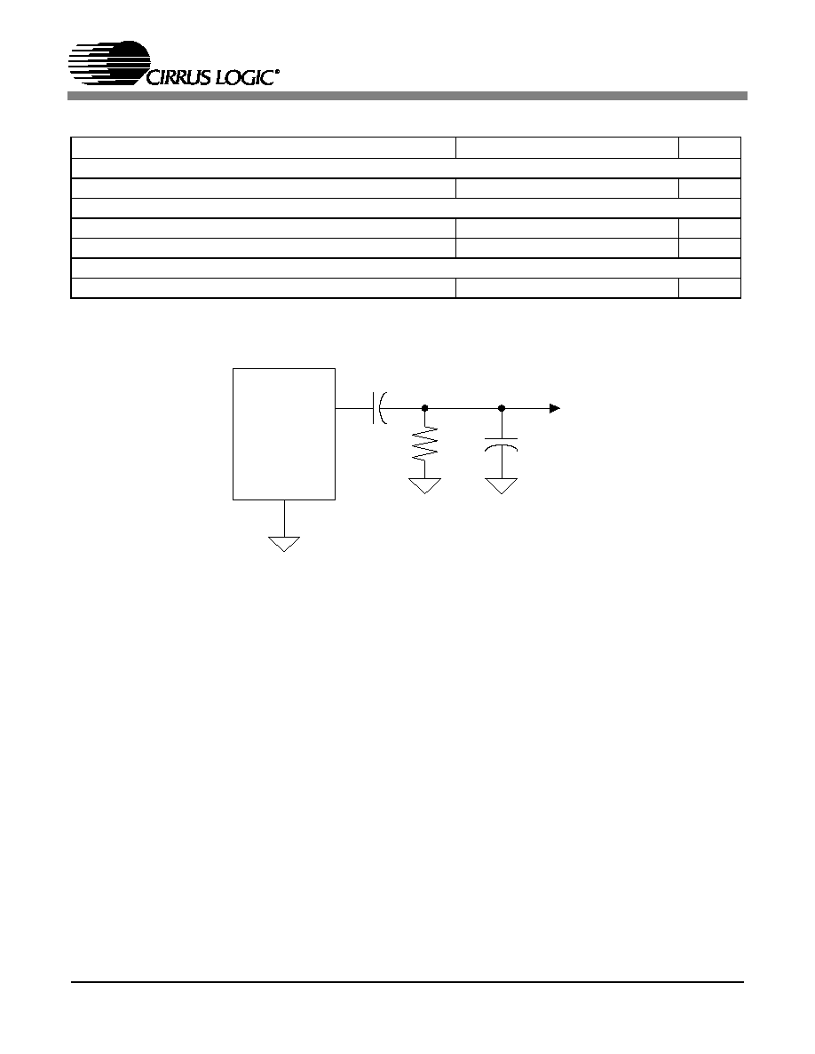
+
Figure 10. Output Test Load

CS43L43
DS479PP3
27
COMBINED INTERPOLATION & ON-CHIP ANALOG FILTER RESPONSE
(The
filter characteristics and the X-axis of the response plots have been normalized to the sample rate (Fs) and can be
referenced to the desired sample rate by multiplying the given characteristic by Fs.)
Notes: 2. Referenced to a 1 kHz, full-scale sine wave.
3. For Single-Speed Mode, the measurement bandwidth is 0.5465 Fs to 3 Fs.
For Double-Speed Mode, the measurement bandwidth is 0.577 Fs to 1.4 Fs.
4. De-emphasis is only available in Single-Speed Mode.
Parameter
Min
Typ
Max
Unit
Single-Speed Mode - (2kHz to 50kHz sample rates)
Passband
to -0.05 dB corner
to -3 dB corner
0
0
-
-
0.4535
0.4998
Fs
Fs
Frequency Response 10 Hz to 20 kHz
(Note 2)
-0.02
-
+0.08
dB
StopBand
0.5465
-
-
Fs
StopBand Attenuation
(Note 3)
50
-
-
dB
Group Delay
-
9/Fs
-
s
Passband Group Delay Deviation
0 - 20 kHz
-
±0.36/Fs
-
s
De-emphasis Error (Relative to 1 kHz)
Fs = 32 kHz
(Note 4)
Fs = 44.1 kHz
Fs = 48 kHz
-
-
-
-
-
-
+0.2/-0.1
+0.05/-0.14
+0/-0.22
dB
Double-Speed Mode - (50kHz to 100kHz sample rates)
Passband
to -0.1 dB corner
to -3 dB corner
0
0
-
-
0.4426
0.4984
Fs
Fs
Frequency Response 10 Hz to 20 kHz
0
-
+0.11
dB
StopBand
0.577
-
-
Fs
StopBand Attenuation
(Note 3)
55
-
-
dB
Group Delay
-
4/Fs
-
s
Passband Group Delay Deviation
0 - 40 kHz
0 - 20 kHz
-
-
±1.39/Fs
±0.23/Fs
-
-
s
s

CS43L43
28
DS479PP3
Figure 11. Single-Speed Stopband Rejection
Figure 12. Single-Speed Transition Band
Figure 13. Single-Speed Transition Band (Detail)
Figure 14. Single-Speed Passband Ripple
-100
-90
-80
-70
-60
-50
-40
-30
-20
-10
0
0.0
0.1
0.2
0.3
0.4
0.5
0.6
0.7
0.8
0.9
1.0
Frequency (normalized to Fs)
Am
p
l
i
t
u
d
e
d
B
-100
-90
-80
-70
-60
-50
-40
-30
-20
-10
0
0.40
0.42
0.44
0.46
0.48
0.50
0.52
0.54
0.56
0.58
0.60
Frequency (normalized to Fs)
A
m
pl
i
t
u
de dB
Figure 15. Double-Speed Stopband Rejection
Figure 16. Double-Speed Transition Band

CS43L43
DS479PP3
29
-10
-9
-8
-7
-6
-5
-4
-3
-2
-1
0
0.45
0.46
0.47
0.48
0.49
0.50
0.51
0.52
0.53
0.54
0.55
Frequency (normalized to Fs)
Am
pl
i
t
ude dB
-0.30
-0.25
-0.20
-0.15
-0.10
-0.05
0.00
0.05
0.10
0.15
0.20
0.25
0.30
0.00
0.05
0.10
0.15
0.20
0.25
0.30
0.35
0.40
0.45
0.50
Frequency (normalized to Fs)
A
m
p
l
i
t
ude
d
B
Figure 17. Double-Speed Transition Band (Detail)
Figure 18. Double-Speed Passband Ripple

CS43L43
30
DS479PP3
SWITCHING SPECIFICATIONS - SERIAL AUDIO INTERFACE
(Inputs: Logic "0" =
GND, Logic "1" = VL.)
Notes: 5. This serial clock is required only in Control Port Mode when the MCLK Divide bit is enabled.
Parameters
Symbol Min Max
Units
External SCLK Mode
MCLK Frequency
1.024
51.2
MHz
MCLK Duty Cycle
45
55
%
Input Sample Rate
Single-Speed Mode
Double-Speed Mode
Fs
Fs
2
50
50
100
kHz
kHz
LRCK Duty Cycle
40
60
%
SCLK Pulse Width Low
t
sclkl
20
-
ns
SCLK Pulse Width High
t
sclkh
20
-
ns
SCLK Period
t
sclkw
-
s
SCLK Frequency
-
Hz
SCLK Frequency
(Note 10)
-
Hz
SCLK rising to LRCK edge delay
t
slrd
20
-
ns
SCLK rising to LRCK edge setup time
t
slrs
20
-
ns
SDATA valid to SCLK rising setup time
t
sdlrs
20
-
ns
SCLK rising to SDATA hold time
t
sdh
20
-
ns
2
MCLK
------------------
MCLK
2
------------------
MCLK
4
------------------
sclkh
t
slrs
t
slrd
t
s d lrs
t
sd h
t
sclkl
t
S D A T A
S C LK
L R C K
Figure 19. External Se-
rial Mode Input Timing

CS43L43
DS479PP3
31
SWITCHING CHARACTERISTICS - INTERNAL SERIAL CLOCK
(Inputs: Logic "0" =
GND, Logic "1" = VL.)
Notes: 6. In Internal SCLK Mode, the LRCK duty cycle must be 50%
+/- 1/2 MCLK Period.
Parameters
Symbol Min Typ
Max
Units
Internal SCLK Mode
LRCK Duty Cycle
(Note 6)
-
50
-
%
SCLK Period
t
sclkw
-
-
s
SCLK rising to LRCK edge
t
sclkr
-
-
s
SDATA valid to SCLK rising setup time
t
sdlrs
-
-
ns
SCLK rising to SDATA hold time
Single-Speed Mode
t
sdh
-
-
ns
Double-Speed Mode
t
sdh
-
-
ns
1
SCLK
-----------------
tsclkw
2
------------------
1
512
(
)Fs
---------------------- 10
+
1
512
(
)Fs
---------------------- 15
+
1
384
(
)Fs
---------------------- 15
+
Figure 20. Internal Serial
Mode Input Timing
*The SCLK pulses shown are internal to the CS43L43.
S D A T A
* IN T E R N A L
S C L K
L R C K
s c lk w
t
s d lrs
t
s d h
t
s c lk r
t
S D A TA
LR C K
M C LK
*IN T E R N A L S C LK
1
N
2
N
Figure 21. Internal Serial Clock Generation
* The SCLK pulses shown are internal to the CS43L43.
N equals MCLK divided by SCLK

CS43L43
32
DS479PP3
SWITCHING SPECIFICATIONS - CONTROL PORT INTERFACE
(Inputs: Logic "0" = GND, Logic "1" = VL.)
7. Data must be held for sufficient time to bridge the transition time, t
fc
, of SCL.
Parameter
Symbol
Min
Max
Unit
I
2
C Mode
SCL Clock Frequency
f
scl
-
100
kHz
RST Rising Edge to Start
t
irs
-
s
Bus Free Time Between Transmissions
t
buf
4.7
-
µs
Start Condition Hold Time (prior to first clock pulse)
t
hdst
4.0
-
µs
Clock Low time
t
low
4.7
-
µs
Clock High Time
t
high
4.0
-
µs
Setup Time for Repeated Start Condition
t
sust
4.7
-
µs
SDA Hold Time from SCL Falling
(Note 7)
t
hdd
0
-
µs
SDA Setup time to SCL Rising
t
sud
250
-
ns
Rise Time of SCL
t
rc
-
25
ns
Fall Time of SCL
t
fc
-
25
ns
Rise Time SDA
t
rd
-
1
µs
Fall Time of SDA
t
fd
-
300
ns
Setup Time for Stop Condition
t
susp
4.7
-
µs
1
2
( )Fs
---------------
Figure 22. Control Port Timing -
I
2
C Mode
t
buf
t
hdst
t
hdst
t
lo w
t r
t f
t
hdd
t
high
t sud
t sust
t susp
Stop
S ta rt
S ta rt
Stop
R e p e a te d
S D A
S C L
t
irs
R S T

CS43L43
DS479PP3
33
DC ELECTRICAL CHARACTERISTICS
(GND = 0V; all voltages with respect to GND.)
DIGITAL INPUT CHARACTERISTICS AND SPECIFICATIONS
(GND = 0V; all voltages
with respect to GND.)
THERMAL CHARACTERISTICS AND SPECIFICATIONS
Parameters
Symbol
Min
Typ
Max
Units
Normal Operation
(Note 8)
Power Supply Current
VA=1.8V
VA_HP=1.8V
VL=1.8V
I
A
I
A_HP
I
D_L
-
-
-
7.3
1.5
4
-
-
-
mA
mA
µA
Power Supply Current
VA=3.0V
VA_HP=3.0V
VL=3.0V
I
A
I
A_HP
I
D_L
-
-
-
10.5
1.5
9.3
-
-
-
mA
mA
µA
Total Power Dissipation
All Supplies=1.8V
All Supplies=3.0V
-
-
16
36
20
50
mW
mW
Power-down Mode
(Note 9)
Power Supply Current
VA=1.8V
VA_HP=1.8V
VL=1.8V
I
A
I
A_HP
I
D_L
-
-
-
2.0
9.3
2.2
-
-
-
µA
µA
µA
Power Supply Current
VA=3.0V
VA_HP=3.0V
VL=3.0V
I
A
I
A_HP
I
D_L
-
-
-
3.4
9.8
7.6
-
-
-
µA
µA
µA
Total Power Dissipation
All Supplies=1.8V
All Supplies=3.0V
-
-
24.3
62.4
-
-
µW
µW
All Modes of Operation
Power Supply Rejection Ratio
(Note 10)
1 kHz
60 Hz
PSRR
-
-
60
40
-
-
dB
dB
V
Q
Nominal Voltage
Output Impedance
Maximum allowable DC current source/sink
V
Q_HP
-
-
-
0.5∑VA
250
0.01
-
-
-
V
k
mA
Filt+ Nominal Voltage
Output Impedance
Maximum allowable DC current source/sink
-
-
-
VA
250
0.01
-
-
-
V
k
mA
Parameters
Symbol Min Typ
Max
Units
Input Leakage Current
I
in
-
-
±10
µA
Input Capacitance
-
8
-
pF
High-Level Input Voltage
V
IH
0.7 x VL
-
-
V
Low-Level Input Voltage
V
IL
-
-
0.3 x VL
V
Parameters
Symbol Min Typ
Max
Units
Package Thermal Resistance
JA
-
75
-
∞C/Watt
Ambient Operating Temperature
(Power Applied)
T
A
-10
-
+70
∞C
CS43L43
34
DS479PP3
RECOMMENDED OPERATING CHARACTERISTICS
(GND = 0V; all voltages with respect
to GND.)
ABSOLUTE MAXIMUM RATINGS
(GND = 0 V; all voltages with respect to AGND. Operation
beyond these limits may result in permanent damage to the device. Normal operation is not guaranteed at these
extremes.)
Notes: 8. Normal operation is defined as RST = HI with a 997 Hz, 0dBFS input sampled at F
s
= 48kHz, and open
outputs, unless otherwise stated.
9. Power Down Mode is defined as RST = LO with all clocks and data lines held static.
10. Valid with the recommended capacitor values on FILT+ and VQ_HP as shown in Figure 1. Increasing
the capacitance will also increase the PSRR. NOTE: Care should be taken when selecting capacitor
type, as any leakage current in excess of 1.0 µA will cause degradation in analog performance.
11. To prevent clipping the outputs, VA_HP
MIN
is limited by the Full-Scale Output Voltage V
FS_HP
, where
VA_HP must be 200 mV greater than V
FS_HP
. However, if distortion is not a concern, VA_HP may be
as low as 0.9 V at any time.
Parameters
Symbol Min Typ
Max
Units
DC Power Supply
Analog
VA
1.7
2.25
3.0
1.8
2.5
3.3
1.9
2.75
3.6
V
V
V
Headphone
(Note 11)
VA_HP
0.9
-
3.6
V
Logic
VL
1.7
2.25
3.0
1.8
2.5
3.3
1.9
2.75
3.6
V
V
V
Parameters
Symbol
Min
Max
Units
DC Power Supplies: Positive Analog
Headphone
Digital I/O
VA
VA_HP
VL
-0.3
-0.3
-0.3
4.0
4.0
4.0
V
V
V
Input Current, Any Pin Except Supplies
I
in
-
±10
mA
Digital Input Voltage
V
IND
-0.3
VL + 0.4
V
Ambient Operating Temperature (power applied)
T
A
-55
125
∞C
Storage Temperature
T
stg
-65
150
∞C

CS43L43
DS479PP3
35
7.0 PARAMETER DEFINITIONS
Total Harmonic Distortion + Noise (THD+N)
The ratio of the rms value of the signal to the rms sum of all other spectral components over the specified
bandwidth (typically 10Hz to 20kHz), including distortion components. Expressed in decibels.
Dynamic Range
The ratio of the full scale rms value of the signal to the rms sum of all other spectral components over the
specified bandwidth. Dynamic range is a signal-to-noise measurement over the specified bandwidth made
with a -60 dBFS signal. 60 dB is then added to the resulting measurement to refer the measurement to full
scale. This technique ensures that the distortion components are below the noise level and do not affect the
measurement. This measurement technique has been accepted by the Audio Engineering Society,
AES17-1991, and the Electronic Industries Association of Japan, EIAJ CP-307.
Interchannel Isolation
A measure of crosstalk between the left and right channels. Measured for each channel at the converter's
output with all zeros to the input under test and a full-scale signal applied to the other channel. Units in deci-
bels.
Interchannel Gain Mismatch
The gain difference between left and right channels. Units in decibels.
Gain Error
The deviation from the nominal full scale analog output for a full scale digital input.
Gain Drift
The change in gain value with temperature. Units in ppm/∞C.
8.0 REFERENCES
1) CDB43L43 Evaluation Board Datasheet
2) "The I
2
C-Bus Specification: Version 2.1" Philips Semiconductors, January 2000.
http://www.semiconductors.philips.com

CS43L43
36
DS479PP3
9.0 PACKAGE DIMENSIONS
Notes: 1. "D" and "E1" are reference datums and do not included mold flash or protrusions, but do include mold
mismatch and are measured at the parting line, mold flash or protrusions shall not exceed 0.20 mm per
side.
2. Dimension "b" does not include dambar protrusion/intrusion. Allowable dambar protrusion shall be
0.13 mm total in excess of "b" dimension at maximum material condition. Dambar intrusion shall not
reduce dimension "b" by more than 0.07 mm at least material condition.
3. These dimensions apply to the flat section of the lead between 0.10 and 0.25 mm from lead tips.
INCHES
MILLIMETERS
NOTE
DIM
MIN
NOM
MAX
MIN
NOM
MAX
A
--
--
0.043
--
--
1.10
A1
0.002
--
0.006
0.05
--
0.15
A2
0.033
0.035
0.037
0.85
0.90
0.95
b
0.008
--
0.012
0.19
--
0.30
2,3
D
--
0.197
--
--
5.00
--
1
E
--
0.252
--
--
6.40
--
E1
0.169
0.173
0.177
4.30
4.40
4.50
1
e
--
0.026
--
--
0.65
--
L
0.020
0.024
0.028
0.50
0.60
0.70
0∞
--
8∞
0∞
--
8∞
JEDEC #: MO-150
16L TSSOP PACKAGE DRAWING
E
N
1 2 3
e
b
A1
A2
A
D
SEATING
PLANE
E1
L
SIDE VIEW
END VIEW
TOP VIEW