1
Copyright
© Cirrus Logic, Inc. 2002
(All Rights Reserved)
P.O. Box 17847, Austin, Texas 78760
(512) 445 7222 FAX: (512) 445 7581
http://www.cirrus.com
Preliminary Product Information
This document contains information for a new product.
Cirrus Logic reserves the right to modify this product without notice.
CS49400 Family DSP
Multi-Standard Audio Decoder
Features
CS49300 Legacy Audio Decoder Support
Dolby Digital EX
TM
, Dolby Pro Logic II
TM
DTS-ES 96/24
TM
, DTS 96/24
TM
, DTS-ES
Discrete 6.1
TM
, DTS-ES Matrix 6.1
TM
, DTS
Digital Surround
TM
and DTS Virtual 5.1
TM
MPEG-2: AAC Multichannel 5.1
MPEG Multichannel and Musicam
MPEG-1/2, Layer III (MP3)
DTS Neo:6
TM
, LOGIC7
Æ
, SRS Circle
Surround II
TM
Cirrus Extra Surround
TM
, Cirrus Original
Surround 6.1 (C.O.S. 6.1)
TM
THX Surround EX
TM
, THX Ultra2 Cinema
TM
12-Channel Serial Audio Inputs
Integrated 8K Byte Input Buffer
Powerful 32-bit Audio DSP
Customer Software Security Keys
Large On-chip X,Y, and Program RAM
Supports SDRAM, SRAM, FLASH
memories
16-channel PCM output
Dual S/PDIF Transmitters
SPI Serial, and Motorola
Æ
and Intel
Æ
Parallel
Host Control Interfaces
GPIO support for all common sub-circuits
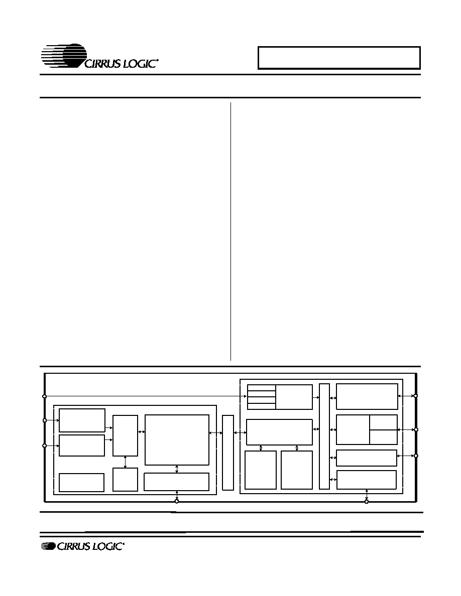
Description
The CS49400 Audio Decoder DSP is targeted as a market-
specific consumer entertainment processor for AV Receivers
and DVD Audio/Video Players. The device is constructed using
an enhanced version of the CS49300 Family DSP audio
decoder followed by a 32-bit programmable post-processor
DSP, which gives the designer the ability to add product
differentiation through the Cirrus Framework
TM
programming
structure and Framework module library. Dolby Digital Pro
Logic II, DTS Digital Surround, MPEG Multichannel, and Cirrus
Original Surround 6.1 PCM Effects Processor (capable of
generating such DSP audio modes as: Hall, Theater, Church)
are included in the cost of the CS49400 Family DSP. Additional
algorithms available through the Crystal Ware
TM
Software
Licensing Program, give the designer the ability to further
deliver end-product differentiation.
The CS49400 contains sufficient on-chip SRAM to support
decoding all major audio decoding algorithms available today
including: AAC Multichannel, DTS 96/24, DTS-ES 96/24. The
CS49400 also
supports a
glueless SDRAM/SRAM for
increased all-channel delays. The SRAM interface also
supports connection to an external byte-wide EPROM for code
storage or Flash memory thus allowing products to be field-
upgradable as new audio algorithms are developed.
This chip, teamed with Crystal Ware
TM
certified decoder
library, Cirrus digital interface products and mixed signal data
converters, enables the conception and design of next
generation digital entertainment products.
Ordering Information:
See
page 98
Parallel or Serial
Host Interface
External Memory
Interface
Inter
nal Bus
32-Bit DSP
Multi-Standard
Audio Decoder
Compressed
Digital
Interface
PLL Clock
Manager
S
h
ared Memor
y
GPIO and I/O
Controller
Digital
Audio
Input
Digital
Audio
Output
DSP C
DSP AB
Serial
Audio
Interface
SAI 0
SAI 1
SAI 3
SAI 2
DAO 0
DAO 1
Frame
Shifter
Input
Buffer
RAM
DSP
RAM
DSP
ROM
Parallel or Serial
Host Interface
Programmable
JUL `02
DS536PP2

2
TABLE OF CONTENTS
1.0 CHARACTERISTICS AND SPECIFICATIONS ...................................................................... 8
1.1 Absolute Maximum Ratings ............................................................................................... 8
1.2 Recommended Operating Conditions ................................................................................ 8
1.3 Digital D.C. Characteristics for VDD Level I/O ................................................................... 8
1.4 Digital D.C. Characteristics for VDDSD Level I/O .............................................................. 9
1.5 Power Supply Characteristics ............................................................................................ 9
1.6 Switching Characteristics-- RESET .................................................................................. 9
1.7 Switching Characteristics -- CLKIN ................................................................................. 10
1.8 Switching Characteristics -- Intel
Æ
Host Slave Mode (DSPAB) ...................................... 11
1.9 Switching Characteristics -- Intel
Æ
Host Slave Mode (DSPC) ........................................ 13
1.10 Switching Characteristics -- Motorola
Æ
Host Slave Mode (DSPAB) ............................ 15
1.11 Switching Characteristics -- Motorola
Æ
Host Slave Mode (DSPC) .............................. 17
1.12 Switching Characteristics -- SPI Control Port Slave Mode (DSPAB) ............................ 19
1.13 Switching Characteristics -- SPI Control Port Slave Mode (DSPC) .............................. 21
1.14 Switching Characteristics -- Digital Audio Input (DSPAB) ............................................ 23
1.15 Switching Characteristics -- Serial Audio Input (DSPC) ............................................... 24
1.16 Switching Characteristics -- CMPDAT, CMPCLK (DSPAB) ......................................... 25
1.17 Switching Characteristics -- Parallel Data Input (DSPAB) ............................................ 26
1.18 Switching Characteristics -- Digital Audio Output ......................................................... 27
1.19 Switching Characteristics -- SRAM/FLASH Interface ................................................... 29
1.20 Switching Characteristics -- SDRAM Interface ............................................................. 31
2. OVERVIEW ............................................................................................................................. 35
Contacting Cirrus Logic Support
For a complete listing of Direct Sales, Distributor, and Sales Representative contacts, visit the Cirrus Logic web site at:
http://www.cirrus.com/corporate/contacts/sales.cfm
Dolby Digital, Dolby Digital EX, AC-3, Dolby Pro Logic, Dolby Pro Logic II, Dolby Digital EX Pro Logic II, Dolby Surround, Dolby Surround Pro Logic
II, Surround EX, Virtual Dolby Digital and the "AAC" logo are trademarks and the "Dolby" and the double-"D" symbol are registered trademarks of
Dolby Laboratories Licensing Corporation. DTS, DTS Digital Surround, DTS-ES Extended Surround, DTS 96/24, DTS-ES 96/24, DTS Neo:6, and
DTS Virtual 5.1 are trademarks and the "DTS", "DTS Digital Surround", "DTS-ES", "DTS 96/24", "DTS-ES 96/24", "DTS Neo:6", "DTS Virtual 5.1" logos
are registered trademarks of the Digital Theater Systems Corporation. The "MPEG Logo" is a registered trademark of Philips Electronics N.V. THX
Ultra2 Cinema, Timbre-Matching, Re-EQ, Adapative Decorrelation and THX are trademarks or registered trademarks of Lucasfilm, Ltd. Surround EX
is a jointly developed technology of THX and Dolby Labs, Inc. AAC (Advanced Audio Coding) is an "MPEG-2-standard-based" digital audio
compression algorithm (offering up 5.1 discrete decoded channels for this implementation) collaboratively developed by AT&T, the Fraunhofer
Institute, Dolby Laboratories, and the Sony Corporation. In regards to the MP3 capable functionality of the CS494XX Family DSP (via downloading
of mp3_ab_494xxx_vv.uld application code) the following statements are applicable: "Supply of this product conveys a license for personal, private
and non-commercial use. MPEG Layer-3 audio decoding technology licensed from Fraunhofer IIS and THOMSON Multimedia." VMAx is a registered
trademark of Harman International. The LOGIC7 logo and LOGIC7 are registered trademarks of Lexicon. SRS CircleSurround, SRS Circle Suround
II, SRS TruSurround, and SRS TruSurround XT are trademarks of SRS Labs, Inc. The HDCD logo, HDCD, High Definition Compatible Digital and
Pacific Microsonics are either registered trademarks or trademarks of Pacific Microsonics, Inc. in the United States and/or other countries. HDCD
technology provided under license from Pacific Microsonics, Inc. This product's software is covered by one or more of the following in the United
States: 5,479,168; 5,638,074; 5,640,161; 5,872,531; 5,808,574; 5,838,274; 5,854,600; 5,864,311; and in Australia: 669114; with other patents
pending. Intel is a registered trademark of Intel Corporation. Motorola is a registered trademark of Motorola, Inc. I
2
C is a registered trademark of Philips
Semiconductor. Purchase of I
2
C Components of Cirrus Logic, Inc., or one of its sublicensed Associated Companies conveys a license under the
Philips I
2
C Patent Rights to use those components in a standard I
2
C system. "Crystal Ware", "Cirrus Framework", "Cirrus Extra Surround", "Cirrus
Triple Crossover Bass Management", "Cirrus Quadruple Crossover Bass Management" and "Cirrus Original Surround 6.1" are trademarks and "Cirrus
Logic" is a registered trademarks of Cirrus Logic, Inc. All other names are trademarks, registered trademarks, or service marks of their respective
companies.
Preliminary product information describes products which are in production, but for which full characterization data is not yet available. Advance
product information describes products which are in development and subject to development changes. Cirrus Logic, Inc. has made best efforts to
ensure that the information contained in this document is accurate and reliable. However, the information is subject to change without notice and is
provided "AS IS" without warranty of any kind (express or implied). No responsibility is assumed by Cirrus Logic, Inc. for the use of this information,
nor for infringements of patents or other rights of third parties. This document is the property of Cirrus Logic, Inc. and implies no license under patents,
copyrights, trademarks, or trade secrets. No part of this publication may be copied, reproduced, stored in a retrieval system, or transmitted, in any
form or by any means (electronic, mechanical, photographic, or otherwise) without the prior written consent of Cirrus Logic, Inc. Items from any Cirrus
Logic website or disk may be printed for use by the user. However, no part of the printout or electronic files may be copied, reproduced, stored in a
retrieval system, or transmitted, in any form or by any means (electronic, mechanical, photographic, or otherwise) without the prior written consent of
Cirrus Logic, Inc.Furthermore, no part of this publication may be used as a basis for manufacture or sale of any items without the prior written consent
of Cirrus Logic, Inc. The names of products of Cirrus Logic, Inc. or other vendors and suppliers appearing in this document may be trademarks or
service marks of their respective owners which may be registered in some jurisdictions. A list of Cirrus Logic, Inc. trademarks and service marks can
be found at http://www.cirrus.com.

3
2.1 DSPAB ............................................................................................................................ 36
2.2 DSPC ............................................................................................................................... 36
3. TYPICAL CONNECTION DIAGRAMS ................................................................................... 37
3.1 Multiplexed Pins .............................................................................................................. 37
3.2 Termination Requirements .............................................................................................. 37
3.3 Phase Locked Loop Filter ................................................................................................ 37
4. POWER
.............................................................................................................................. 38
4.1 Decoupling ....................................................................................................................... 38
4.2 Analog Power Conditioning ............................................................................................. 38
4.3 Ground ............................................................................................................................. 38
4.4 Pads ................................................................................................................................ 38
5. CLOCKING ............................................................................................................................. 42
6. CONTROL .............................................................................................................................. 42
6.1 Serial Communication ..................................................................................................... 42
6.1.1 SPI Communication for DSPAB .......................................................................... 42
6.1.2 SPI Communication for DSPC ............................................................................ 46
6.1.3 FINTREQ Behavior: A Special Case .................................................................. 49
6.2 Parallel Host Communication for DSPAB ........................................................................ 51
6.2.5 Intel Parallel Host Communication Mode for DSPAB ......................................... 51
6.2.6 Motorola Parallel Communication Mode for DSPAB ........................................... 54
6.2.7 Procedures for Parallel Host Mode Communication for DSPAB ......................... 56
6.3 Parallel Host Communication for DSPC .......................................................................... 58
6.3.5 Intel Parallel Host Communication Mode for DSPC ............................................ 60
6.3.6 Motorola Parallel Host Communication Mode for DSPC .................................... 64
6.3.7 Procedures for Parallel Host Mode Communication for DSPC ........................... 68
7. EXTERNAL MEMORY ............................................................................................................ 70
7.1 Configuring SRAM Timing Parameters ........................................................................... 71
8. BOOT PROCEDURE .............................................................................................................. 72
8.1 Host Controlled Master Boot ........................................................................................... 72
8.2 Host Boot Via DSPC ........................................................................................................ 75
9. SOFT RESETTING THE CS49400 ......................................................................................... 77
9.1 Host Controlled Master Soft Reset .................................................................................. 77
10. HARDWARE CONFIGURATION ......................................................................................... 79
11. DIGITAL INPUT AND OUTPUT DATA FORMATS .............................................................. 79
11.1 Digital Audio Formats .................................................................................................... 79
11.1.1 I
2
S ..................................................................................................................... 79
11.1.2 Left Justified ...................................................................................................... 79
11.2 Digital Audio Input Port .................................................................................................. 79
11.3 Compressed Data Input Port ......................................................................................... 80
11.4 Input Data Hardware Configuration for CDI and DAI on DSPAB ................................. 80
11.4.1
Input Configuration Considerations ................................................................ 81
11.5 Serial Audio Input .......................................................................................................... 82
11.6 Digital Audio Output Port ............................................................................................... 82
11.6.1 S/PDIF Outputs ................................................................................................. 83
11.7 Output Data Hardware Configuration ............................................................................ 84
11.8 Creating Hardware Configuration Messages ................................................................. 85
12.0 PIN DESCRIPTION ............................................................................................................. 87
12.1 144-Pin LQFP Package Pin Layout ............................................................................... 87
12.2 100-Pin LQFP Package Pin Layout ............................................................................... 88
12.3 Pin Definitions ................................................................................................................ 89
13. ORDERING INFORMATION ................................................................................................ 99
14. PACKAGE DIMENSIONS .................................................................................................. 100
14.1 144-Pin LQFP Package ............................................................................................... 100

4
LIST OF FIGURES
Figure 1. RESET Timing ..................................................................................................................... 9
Figure 2. CLKIN with CLKSEL = VSS = PLL Enable ........................................................................ 10
Figure 3. Intel
Æ
Parallel Host Mode Slave Read Cycle for DSPAB .................................................. 12
Figure 4. Intel
Æ
Parallel Host Mode Slave Write Cycle for DSPAB ................................................... 12
Figure 5. Intel
Æ
Parallel Host Slave Mode Read Cycle for DSPC ..................................................... 14
Figure 6. Intel
Æ
Parallel Host Slave Mode Write Cycle for DSPC ..................................................... 14
Figure 7. Motorola
Æ
Parallel Host Slave Mode Read Cycle for DSPAB ........................................... 16
Figure 8. Motorola
Æ
Parallel Host Slave Mode Write Cycle for DSPAB ........................................... 16
Figure 9. Motorola
Æ
Parallel Host Slave Mode Read Cycle for DSPC ............................................. 18
Figure 10. Motorola
Æ
Parallel Host Slave Mode Write Cycle for DSPC ............................................ 18
Figure 11. SPI Control Port Slave Mode Timing (DSPAB) ............................................................... 20
Figure 12. SPI Control Port Slave Mode Timing (DSPC) ................................................................. 22
Figure 13. Digital Audio Input Data, Slave Clock Timing .................................................................. 23
Figure 14. Serial Audio Input Data, Slave Clock Timing ................................................................... 24
Figure 15. Serial Compressed Data Timing ...................................................................................... 25
Figure 16. Parallel Data Timing ........................................................................................................ 26
Figure 17. Digital Audio Output Data, Input and Output Clock Timing ............................................. 28
Figure 18. Digital Audio Output Data, Input and Output Clock Timing ............................................. 28
Figure 19. SRAM/Flash Controller Timing Diagram - Write Cycle .................................................... 29
Figure 20. SRAM/Flash Controller Timing Diagram - Read Cycle .................................................... 29
Figure 21. SRAM/Flash Controller Timing Diagram - Single Byte Write Cycle ................................. 30
Figure 22. SRAM/Flash Controller Timing Diagram - Single Byte Read Cycle ................................ 30
Figure 23. SDRAM Controller Timing Diagram - Load Mode Register Cycle ................................... 31
Figure 24. SDRAM Controller Timing Diagram - Burst Write Cycle .................................................. 32
Figure 25. SDRAM Controller Timing Diagram - Burst Read Cycle ................................................. 33
Figure 26. SDRAM Controller Timing Diagram - Auto Refresh Cycle .............................................. 34
Figure 27. SPI Control with External Memory - 144 Pin Package .................................................... 39
Figure 28. Intel
Æ
Parallel Control Mode - 144 Pin Package .............................................................. 40
Figure 29. Motorola
Æ
Parallel Control Mode - 144 Pin Package ....................................................... 41
Figure 30. SPI Write Flow Diagram for DSPAB ................................................................................ 43
Figure 31. SPI Timing for DSPAB ..................................................................................................... 44
Figure 32. SPI Read Flow Diagram for DSPAB ................................................................................ 45
Figure 33. SPI Write Flow Diagram for DSPC .................................................................................. 46
Figure 34. SPI Timing for DSPC ....................................................................................................... 47
Figure 35. SPI Read Flow Diagram for DSPC .................................................................................. 48
Figure 36. Intel Mode, One-Byte Write Flow Diagram for DSPAB .................................................... 53
Figure 37. Intel Mode, One-Byte Read Flow Diagram for DSPAB ................................................... 54
Figure 38. Motorola Mode, One-Byte Write Flow Diagram for DSPAB ............................................ 55
Figure 39. Motorola Mode, One-Byte Read Flow Diagram for DSPAB ............................................ 55
Figure 40. Typical Parallel Host Mode Control Write Sequence Flow Diagram for DSPAB ............. 56
Figure 41. Typical Parallel Host Mode Control Read Sequence Flow Diagram for DSPAB ............. 57

5
Figure 42. Intel Mode, One-Byte Write Flow Diagram for DSPC .......................................................60
Figure 44. Intel Mode, One-Byte Read Flow Diagram for DSPC ......................................................61
Figure 43. Intel Mode, 32-bit (4-byte) Write Flow
Diagram for DSPC .............................................................................................................................62
Figure 45. Intel Mode, 32-Bit (4-Byte) Read Flow
Diagram for DSPC .............................................................................................................................63
Figure 46. Motorola Mode, One-Byte Write Flow
Diagram for DSPC .............................................................................................................................64
Figure 47. Motorola Mode, 32-bit (4-byte) Write Flow Diagram for DSPC ........................................65
Figure 48. Motorola Mode, One-Byte Read Flow
Diagram for DSPC .............................................................................................................................66
Figure 49. Motorola Mode, 32-Bit (4-Byte) Read Flow Diagram for DSPC .......................................67
Figure 50. Typical Parallel Host Mode Control Write Sequence Flow Diagram for DSPC ................68
Figure 51. Typical Parallel Host Mode Control Read Sequence Flow Diagram for DSPC ................69
Figure 52. Host Controlled Master Boot
(Downloading both a DSPAB Application Code and a DSPC Application Code) ..............................73
Figure 53. Host Boot Via DSPC .......................................................................................................76
Figure 54. Host Controlled Master Softreset .....................................................................................78
Figure 55. I
2
S Format ........................................................................................................................80
Figure 56. Left Justified Format (Rising Edge Valid SCLK) ...............................................................80
Figure 57. Pin Layout (144-Pin LQFP Package) ...............................................................................87
Figure 58. Pin Layout (100-Pin LQFP Package) ...............................................................................88
Figure 59. 144-Pin LQFP Package Drawing ...................................................................................100

6
LIST OF TABLES
Table 1. PLL Filter Component Values ...............................................................................................37
Table 2. Host Modes for DSPAB ........................................................................................................42
Table 3. Host Modes for DSPC ..........................................................................................................42
Table 4. SPI Communication Signals for DSPAB ...............................................................................43
Table 5. SPI Communication Signals for DSPC .................................................................................46
Table 6. Intel Mode Communication Signals for DSPAB ....................................................................51
Table 6. Parallel Input/Output Registers for DSPAB ..........................................................................52
Table 7. Motorola Mode Communication Signals for DSPAB.............................................................54
Table 8. Parallel Input/Output Registers for DSPC.............................................................................59
Table 9. Intel Mode Communication Signals for DSPC ......................................................................60
Table 10. Motorola Mode Communication Signals for DSPC .............................................................64
Table 11. SRAM Interface Pins ..........................................................................................................70
Table 12. SDRAM Interface Pins ........................................................................................................70
Table 13. SRAM Controller Timing .....................................................................................................71
Table 14. SDRAM Config Register .....................................................................................................71
Table 15. Application Messages from DSPAB ...................................................................................72
Table 16. Boot Write Messages for DSPC .........................................................................................72
Table 17. Boot Read Messages from DSPC ......................................................................................72
Table 18. Digital Audio Input Port .......................................................................................................80
Table 19. Compressed Data Input Port ..............................................................................................80
Table 20. Input Data Type Configuration
(Input Parameter A).............................................................................................................81
Table 21. Input Data Format Configuration
(Input Parameter B).............................................................................................................81
Table 22. Input SCLK Polarity Configuration
(Input Parameter C) ............................................................................................................81
Table 23. Serial Audio Input Port ........................................................................................................82
Table 24. SAI Data Type Configuration
(Input Parameter D) ............................................................................................................82
Table 25. Digital Audio Output Port ....................................................................................................82
Table 26. MCLK/SCLK Master Mode Ratios ......................................................................................83
Table 27. Output Clock Configuration
(Parameter A)......................................................................................................................84
Table 28. Output Data Configuration Parameter B)...........................................................................84
Table 29. Output SCLK/LRCLK Configuration
(Parameter C) .....................................................................................................................84
Table 30. Output SCLK Polarity Configuration
(Parameter D) .....................................................................................................................85
Table 31. Example Values to be Sent to DSPAB After Download or Soft Reset................................86
Table 32. Example Values to be Sent to DSPC After Download or Soft Reset ..................................86

7
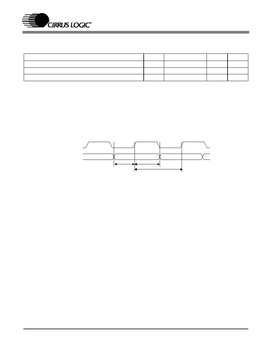
1.0 CHARACTERISTICS AND SPECIFICATIONS
Note: All data sheet minimum and maximum timing parameters are guaranteed over the rated voltage and
temperature. Actual production testing is performed at T
A
= 25 ∞C with an appropriate guardband to
guarantee minimum and maximum timing specifications over rated voltage and temperature.
1.1 Absolute Maximum Ratings
(VSS, VSSSD, PLLVSS = 0 V; all voltages with respect to 0 V)
Caution:
Operation at or beyond these limits may result in permanent damage to the device. Normal operation
is not guaranteed at these extremes.
1.2 Recommended Operating Conditions
(VSS, VSSSD, PLLVSS = 0 V; all voltages with respect to 0 V)
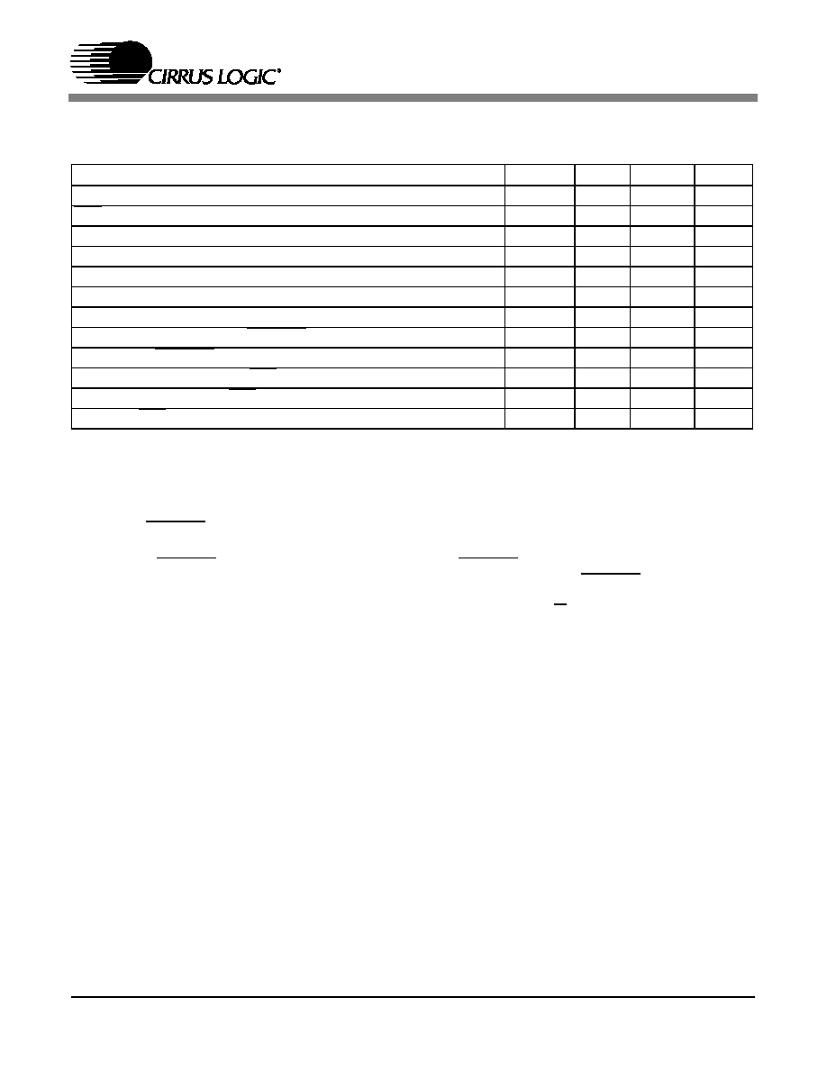
1.3 Digital D.C. Characteristics for VDD Level I/O
(T
A
= 25 ∞C;VDD = 2.5 V; measurements performed under static conditions.)
Parameter
Symbol
Min
Max
Unit
DC power supplies:
Core supply
PLL supply
Memory supply
||PLLVDD| ≠ |VDD||
VDD
PLLVSS
VDDSD
≠0.3
≠0.3
≠0.3
-
2.7
2.7
3.6
0.3
V
V
V
V
Input current, any pin except supplies
I
in
-
±10
mA
Digital input voltage on I/O pins powered from VDD
V
ind
-
3.6
V
Digital input voltage on I/O pins powered from VDDSD
V
insd
-
3.6
V
Storage temperature
T
stg
≠65
150
∞C
Parameter
Symbol
Min
Typ
Max
Unit
DC power supplies:
Core supply
PLL supply
Memory supply
||PLLVDD| ≠ |VDD||
VDD
PLLVSS
VDDSD
2.37
2.37
3.15
2.5
2.5
3.3
2.63
2.63
3.45
0.3
V
V
V
V
Ambient operating temperature
T
A
0
-
70
∞C
Parameter
Symbol
Min
Typ
Max
Unit
High-level input voltage
V
IH
2.0
-
-
V
Low-level input voltage
V
IL
-
-
0.8
V
High-level output voltage at I
O
= ≠2.0 mA
V
OH
VDD
◊ 0.9
-
-
V
Low-level output voltage at I
O
= 2.0 mA
V
OL
-
-
VDD
◊ 0.1
V
Input leakage current (all pins without internal pull-
up resistors except CLKIN)
I
in
-
-
10
µA
Input leakage current (pins with internal pull-up
resistors, CLKIN)
50
µA
8
1.4 Digital D.C. Characteristics for VDDSD Level I/O
(T
A
= 25 ∞C;VDDSD = 3.3 V±; measurements performed under static conditions.)
1.5 Power Supply Characteristics
(T
A
= 25 ∞C; VDD, PLLVDD = 2.5 V; VDDSD = 3.3 V;measurements performed under operating conditions)
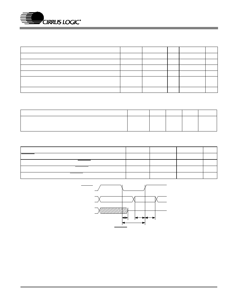
1.6 Switching Characteristics-- RESET
(T
A
= 25 ∞C; VDD, PLLVDD= 2.5 V; VDDSD = 3.3 V; C
L
= 20 pF)
Parameter
Symbol
Min
Typ
Max
Unit
High-level input voltage
V
IH
0.65xVDDSD
V
Low-level input voltage
V
IL
0.35xVDDSD
V
High-level output voltage at I
O
= ≠2.0 mA
V
OH
0.9xVDDSD
V
Low-level output voltage at I
O
= 2.0 mA
V
OL
0.1xVDDSD
V
Input leakage current (except all pins with internal pull-
up)
I
in
10
µA
Input leakage current (all pins with internal pull-up)
50
µA
Parameter
Symbol
Min
Typ
Max
Unit
Power supply current:
Core and I/O operating: VSS
PLL operating: PLLVSS
Memory operating: VSSSD
400
6
25
mA
mA
mA
Parameter
Symbol
Min
Max
Unit
RESET minimum pulse width low
T
rstl
10
-
µs
All bidirectional pins high-Z after RESET low
T
rst2z
50
ns
Configuration bits setup before RESET high
T
rstsu
50
-
ns
Configuration bits hold after RESET high
T
rsthld
15
-
ns
RESET
T
rst2z
T
rstl
T
rstsu
T
rsthld
FHS0,1,2
UHS0,1,2
All Bidirectional
Pins
Figure 1. RESET Timing
9
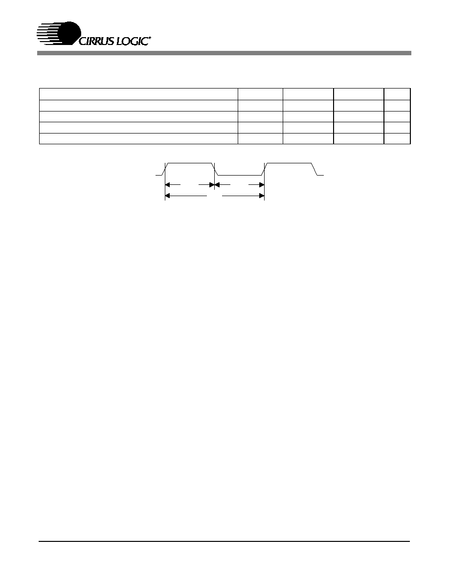
1.7 Switching Characteristics -- CLKIN
(T
A
= 25 ∞C; VDD, PLLVDD = 2.5; VDDSD = 3.3 V; C
L
= 20 pF)
Parameter
Symbol
Min
Max
Unit
CLKIN period for internal DSP clock mode
T
clki
35
100
ns
CLKIN high time for internal DSP clock mode
T
clkih
18
ns
CLKIN low time for internal DSP clock mode
T
clkil
18
ns
External Crystal operating frequency
F
xtal
10
14
MHz
CL KIN
T
clkih
T
clkil
T
clki
Figure 2. CLKIN with CLKSEL = VSS = PLL Enable

10
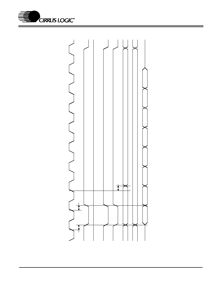
1.8 Switching Characteristics -- Intel
Æ
Host Slave Mode (DSPAB)
(T
A
= 25 ∞C; VDD, PLLVDD = 2.5 V; VDDSD = 3.3 V; C
L
= 20 pF)
Notes: 1. Certain timing parameters are normalized to the DSP clock period, DCLKP. DCLKP = 1/DCLK. The
DSP clock can be defined as follows:
Internal Clock Mode:
DCLK ~ 60MHz before and during boot, i.e. DCLKP ~ 16.6ns
DCLK ~ 86 MHz after boot, i.e. DCLKP ~ 11.6ns
It should be noted that DCLK for the internal clock mode is application specific. The application code
users guide should be checked to confirm DCLK for the particular application.
Parameter
Symbol
Min
Max
Unit
Address setup before FCS and FRD low or FCS and FWR low
T
ias
5
-
ns
Address hold time after FCS and FRD low or FCS and FWR
high
T
iah
5
-
ns
Read
Delay between FRD then FCS low or FCS then FRD low
T
icdr
0
-
ns
Data valid after FCS and FRD low
T
idd
-
21
ns
FCS and FRD low for read
(Note 1)
T
irpw
DCLKP + 10
-
ns
Data hold time after FCS or FRD high
T
idhr
5
-
ns
Data high-Z after FCS or FRD high
T
idis
-
22
ns
FCS or FRD high to FCS and FRD low for next read (Note 1)
T
ird
2*DCLKP + 10
-
ns
FCS or FRD high to FCS and FWR low for next write (Note 1)
T
irdtw
2*DCLKP + 10
-
ns
Write
Delay between FWR then FCS low or FCS then FWR low
T
icdw
0
-
ns
Data setup before FCS or FWR high
T
idsu
20
-
ns
FCS and FWR low for write
(Note 1)
T
iwpw
DCLKP + 10
-
ns
Data hold after FCS or FWR high
T
idhw
5
-
ns
FCS or FWR high to FCS and FRD low for next read (Note 1)
T
iwtrd
2*DCLKP + 10
-
ns
FCS or FWR high to FCS and FWR low for next write (Note 1)
T
iwd
2*DCLKP + 10
-
ns
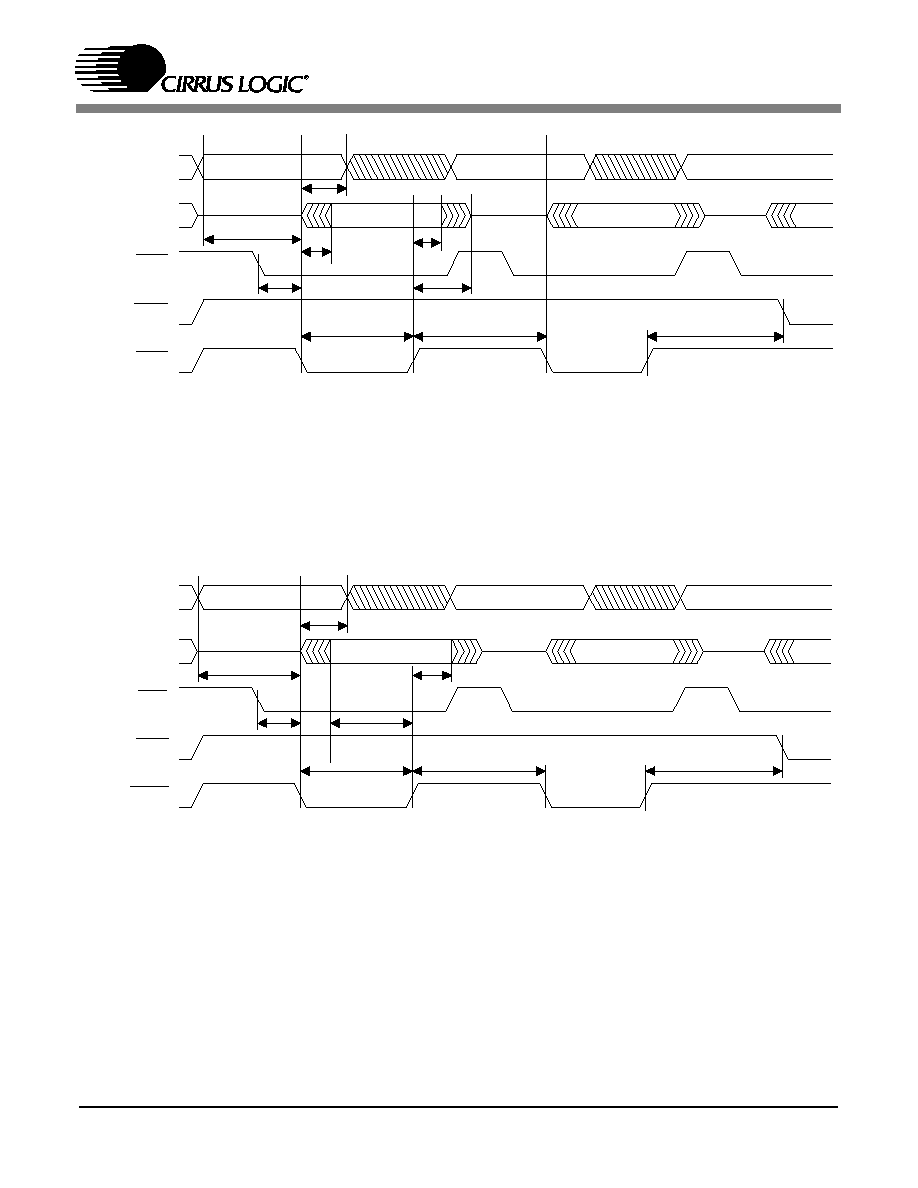
11
Figure 3. Intel
Æ
Parallel Host Mode Slave Read Cycle for DSPAB
DAT A7:0
C S
W R
RD
T
ias
T
icdr
T
idd
T
irpw
T
idhr
T
idis
T
ird
T
irdtw
F
F
F
F
T
ia h
A1:0
F
DATA7:0
CS
R D
W R
T
ias
T
icdw
T
iw pw
T
id hw
T
iw d
T
iw trd
T
idsu
F
F
F
F
T
iah
A1:0
F
Figure 4. Intel
Æ
Parallel Host Mode Slave Write Cycle for DSPAB
12
1.9 Switching Characteristics -- Intel
Æ
Host Slave Mode (DSPC)
(T
A
= 25 ∞C; VDD, PLLVDD = 2.5 V; VDDSD = 3.3 V; C
L
= 20 pF)
Notes: 1. Certain timing parameters are normalized to the DSP clock, DCLKP, in nanoseconds. DCLKP =
1/DCLK. The DSP clock can be defined as follows:
Internal Clock Mode:
DCLK ~ 60MHz before and during boot, i.e. DCLKP ~ 16.6ns
DCLK ~ 86 MHz after boot, i.e. DCLKP ~ 11.6ns
It should be noted that DCLK for the internal clock mode is application specific. The application code
users guide should be checked to confirm DCLK for the particular application.
Parameter
Symbol
Min
Max
Unit
Address setup before CS and RD low or CS and WR low
T
ias
DCLKP
-
ns
Address hold time after CS and RD low or CS and WR low
T
iah
DCLKP+15
-
ns
Read
Delay between RD then CS low or CS then RD low
T
icdr
0
-
ns
Data valid after CS and RD low
T
idd
-
2*DCLKP+
25
ns
CS and RD low for read
(Note 1)
T
irpw
2*DCLKP
-
ns
Data hold time after CS or RD high
T
idhr
DCLKP+10
-
ns
Data high-Z after CS or RD high
T
idis
-
2*DCLKP+
10
ns
CS or RD high to CS and RD low for next read
(Note 1)
T
ird
2*DCLKP+10
-
ns
CS or RD high to CS and WR low for next write
(Note 1)
T
irdtw
2*DCLKP+10
-
ns
Write
Delay between WR then CS low or CS then WR low
T
icdw
0
-
ns
Data setup before CS or WR high
T
idsu
2*DCLKP+10
-
ns
CS and WR low for write
(Note 1)
T
iwpw
2*DCLKP
-
ns
Data hold after CS or WR high
T
idhw
DCLKP
-
ns
CS or WR high to CS and RD low for next read
(Note 1)
T
iwtrd
2*DCLKP+10
-
ns
CS or WR high to CS and WR low for next write
(Note 1)
T
iwd
2*DCLKP+10
-
ns
13
A1:0
DATA7:0
CS
WR
RD
T
ias
T
icdr
T
iah
T
idd
T
irpw
T
idhr
T
idis
T
ird
T
irdtw
Figure 5. Intel
Æ
Parallel Host Slave Mode Read Cycle for DSPC
A1:0
DATA7:0
CS
RD
WR
T
ias
T
icdw
T
iah
T
iwpw
T
idhw
T
iw d
T
iwtrd
T
idsu
Figure 6. Intel
Æ
Parallel Host Slave Mode Write Cycle for DSPC

14
1.10 Switching Characteristics -- Motorola
Æ
Host Slave Mode (DSPAB)
(T
A
= 25 ∞C; VDD, PLLVDD = 2.5 V; VDDSD = 3.3 V; C
L
= 20 pF)
Notes: 1. Certain timing parameters are normalized to the DSP clock, DCLKP, in nanoseconds. DCLKP =
1/DCLK. The DSP clock can be defined as follows:
Internal Clock Mode:
DCLK ~ 60MHz before and during boot, i.e. DCLKP ~ 16.6ns
DCLK ~ 86 MHz after boot, i.e. DCLKP ~ 11.6ns
It should be noted that DCLK for the internal clock mode is application specific. The application code
users guide should be checked to confirm DCLK for the particular application.
Parameter
Symbol
Min
Max
Unit
Address setup before FCS and FDS low
T
mas
5
-
ns
Address hold time after FCS and FDS low
T
mah
5
-
ns
Read
Delay between FDS then FCS low or FCS then FDS low
T
mcdr
0
-
ns
Data valid after FCS and FRD low with R/W high)
T
mdd
-
21
ns
FCS and FDS low for read
(Note 1)
T
mrpw
DCLKP + 10
-
ns
Data hold time after FCS or FDS high after read
T
mdhr
5
-
ns
Data high-Z after FCS or FDS high after read
T
mdis
-
22
ns
FCS or FDS high to FCS and FDS low for next read (Note 1)
T
mrd
2*DCLKP + 10
-
ns
FCS or FDS high to FCS and FDS low for next write(Note 1)
T
mrdtw
2*DCLKP + 10
-
ns
Write
Delay between FDS then FCS low or FCS then FDS low
T
mcdw
0
-
ns
Data setup before FCS or FDS high
T
mdsu
20
-
ns
FCS and FDS low for write
(Note 1)
T
mwpw
DCLKP + 10
-
ns
R/W setup before FCS AND FDS low
T
mrwsu
5
-
ns
R/W hold time after FCS or FDS high
T
mrwhld
5
-
ns
Data hold after FCS or FDS high
T
mdhw
5
-
ns
FCS or FDS high to FCS and FDS low with R/W high for
next read
(Note 1)
T
mwtrd
2*DCLKP + 10
-
ns
FCS or FDS high to FCS and FDS low for next write(Note 1)
T
mwd
2*DCLKP + 10
-
ns

15
DATA7:0
CS
R/W
DS
T
mas
T
mcdr
mah
T
mdd
T
mrpw
T
mdhr
T
mdis
T
mrd
T
mrdtw
T
mrwsu
T
mrwhld
F
F
F
F
T
A1:0
F
Figure 7. Motorola
Æ
Parallel Host Slave Mode Read Cycle for DSPAB
DATA7:0
CS
R/W
DS
T
mas
T
mdsu
T
mdhw
T
mwd
T
mwtrd
T
mwpw
T
mcdw
T
mrwsu
T
mrwhld
F
F
F
F
F
mah
T
A1:0
F
Figure 8. Motorola
Æ
Parallel Host Slave Mode Write Cycle for DSPAB
16
1.11 Switching Characteristics -- Motorola
Æ
Host Slave Mode (DSPC)
(T
A
= 25 ∞C; VDD, PLLVDD = 2.5 V; VDDSD = 3.3 V; C
L
= 20 pF)
Notes: 1. Certain timing parameters are normalized to the DSP clock, DCLKP, in nanoseconds. DCLKP =
1/DCLK. The DSP clock can be defined as follows:
Internal Clock Mode:
DCLK ~ 60MHz before and during boot, i.e. DCLKP ~ 16.6ns
DCLK ~ 86 MHz after boot, i.e. DCLKP ~ 11.6ns
It should be noted that DCLK for the internal clock mode is application specific. The application code
users guide should be checked to confirm DCLK for the particular application.
Parameter
Symbol
Min
Max
Unit
Address setup before CS and DS low
T
mas
DCLKP
-
ns
Address hold time after CS and DS low
T
mah
DCLKP+15
-
ns
Read
Delay between DS then CS low or CS then DS low
T
mcdr
0
-
ns
Data valid after CS and RD low with R/W high
T
mdd
-
2*DCLKP+
25
ns
CS and DS low for read
(Note 1)
T
mrpw
2*DCLKP
-
ns
Data hold time after CS or DS high after read
T
mdhr
DCLKP+ 10
-
ns
Data high-Z after CS or DS high low after read
T
mdis
-
2*DCLKP+
10
ns
CS or DS high to CS and DS low for next read
(Note 1)
T
mrd
2*DCLKP+10
-
ns
CS or DS high to CS and DS low for next write
(Note 1)
T
mrdtw
2*DCLKP+10
-
ns
Write
Delay between DS then CS low or CS then DS low
T
mcdw
0
-
ns
Data setup before CS or DS high
T
mdsu
2*DCLKP+10
-
ns
CS and DS low for write
(Note 1)
T
mwpw
2*DCLKP
-
ns
R/W setup before CS AND DS low
T
mrwsu
DCLKP
-
ns
R/W hold time after CS or DS high
T
mrwhld
5
-
ns
Data hold after CS or DS high
T
mdhw
DCLKP
-
ns
CS or DS high to CS and DS low with R/W high for next read
(Note 1)
T
mwtrd
2*DCLKP+10
-
ns
CS or DS high to CS and DS low for next write
(Note 1)
T
mwd
2*DCLKP+10
-
ns
17
A1:0
DATA7:0
CS
R/W
DS
T
mas
T
mcdr
T
mah
T
mdd
T
mrpw
T
mdhr
T
mdis
T
mrd
T
mrdtw
T
mrwsu
T
mrwhld
Figure 9. Motorola
Æ
Parallel Host Slave Mode Read Cycle for DSPC
A1:0
DATA7:0
CS
R/W
DS
T
mas
T
mdsu
T
mah
T
mdhw
T
mwd
T
mwtrd
T
mwpw
T
mcdw
T
mrwsu
T
mrwhld
Figure 10. Motorola
Æ
Parallel Host Slave Mode Write Cycle for DSPC
18
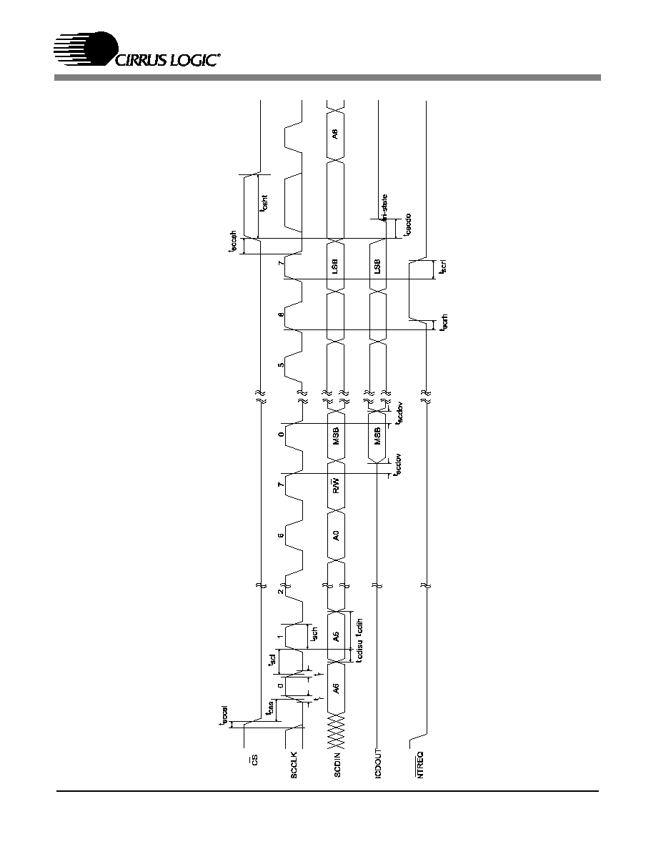
1.12 Switching Characteristics -- SPI Control Port Slave Mode (DSPAB)
(T
A
= 25 ∞C; VDD, PLLVDD = 2.5 V; VDDSD = 3.3 V; C
L
= 20 pF)
Notes: 1. The specification f
sck
indicates the maximum speed of the hardware. The system designer should be
aware that the actual maximum speed of the communication port may be limited by the DSP application
code. The relevant application code user's manual should be consulted for the software speed
limitations.
2. Data must be held for sufficient time to bridge the transition time of FSCCLK.
3. FINTREQ goes high only if there is no data to be read from the DSP at the rising edge of FSCCLK for
the second-to-last bit of the last byte of data during a read operation as shown.
4. If FINTREQ goes high as indicated in (Note 3), then FINTREQ is guaranteed to remain high until the
next rising edge of FSCCLK. If there is more data to be read at this time, FINTREQ goes active low
again. Treat this condition as a new read transaction. Raise chip select to end the current read
transaction and then drop it, followed by the 7-bit address and the R/W bit (set to 1 for a read) to start
a new read transaction.
Parameter
Symbol
Min
Max
Units
FSCCLK clock frequency
(Note 1)
f
sck
-
2
MHz
FCS falling to FSCCLK rising
t
css
20
-
ns
FSCCLK low time
t
scl
150
-
ns
FSCCLK high time
t
sch
150
-
ns
Setup time FSCDIN to FSCCLK rising
t
cdisu
50
-
ns
Hold time FSCCLK rising to FSCDIN
(Note 2)
t
cdih
50
-
ns
Transition time from FSCCLK to FSCDOUT valid
t
scdov
-
40
ns
Time from FSCCLK rising to FINTREQ rising
(Note 3)
t
scrh
-
200
ns
Hold time for FINTREQ from FSCCLK rising
(Note 4, 5)
t
scrl
0
-
ns
Time from FSCCLK falling to FCS rising
t
sccsh
20
-
ns
High time between active FCS
t
csht
200
-
ns
Time from FCS rising to FSCDOUT high-Z
t
cscdo
20
ns
19
t css
t sc
l
t r
t sch
t
cd
isu
t s
c
dov
t cd
ih
t s
c
dov
t f
MS
B
MS
B
A0
A6
A
5
FCS
FS
C
C
L
K
FS
CDI
N
FS
C
D
O
U
T
FI
NT
RE
Q
t sccsh
t scr
l
t scr
h
t csh
t
LSB
LSB
67
5
A6
t cs
c
d
o
tr
i
-
s
t
a
t
e
0
7
6
2
1
0
R/
W
F
i
g
u
r
e
1
1
.
S
P
I
Co
ntr
o
l
P
o
r
t
S
l
a
v
e
M
o
de
T
i
m
i
ng
(DSP
AB
)

20
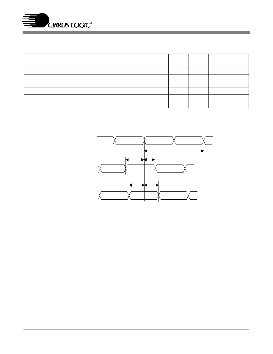
1.13 Switching Characteristics -- SPI Control Port Slave Mode (DSPC)
(T
A
= 25 ∞C; VDD, PLLVDD = 2.5 V; VDDSD = 3.3 V; C
L
= 20 pF)
Notes: 1. The specification f
sck
indicates the maximum speed of the hardware. The system designer should be
aware that the actual maximum speed of the communication port may be limited by the software. The
relevant application code user's manual should be consulted for the software speed limitations.
2. Data must be held for sufficient time to bridge the transition time of SCCLK.
Parameter
Symbol
Min
Max
Units
SCCLK clock frequency
(Note 1)
f
sck
-
5
MHz
CS falling to SCCLK rising
t
css
4*DCLKP
-
ns
SCCLK low time
t
scl
4*DCLKP
-
ns
SCCLK high time
t
sch
4*DCLKP
-
ns
Setup time SCDIN to SCCLK rising
t
cdisu
DCLKP
-
ns
Hold time SCCLK rising to SCDIN
(Note 2)
t
cdih
DCLKP+20
-
ns
Time from SCCLK low to SCDOUT valid
t
scdov
-
3*DCLKP+20
ns
Time from SCCLK rising to INTREQ rising
t
scrh
-
DCLKP
ns
Hold time for INTREQ from SCCLK rising
t
scrl
DCLKP
-
ns
Time from SCCLK falling to CS rising
t
sccsh
2*DCLKP+15
-
ns
Time from SCCLK low to CS falling
t
sccsl
10
ns
High time between active CS
t
csht
4*DCLKP
-
ns
Time from CS rising to SCDOUT high-Z
t
cscdo
DCLKP
ns
21
F
i
g
u
r
e
1
2
.
S
P
I
Co
ntr
o
l
P
o
r
t
S
l
a
v
e
M
o
de
T
i
m
i
ng
(DSP
C)

22
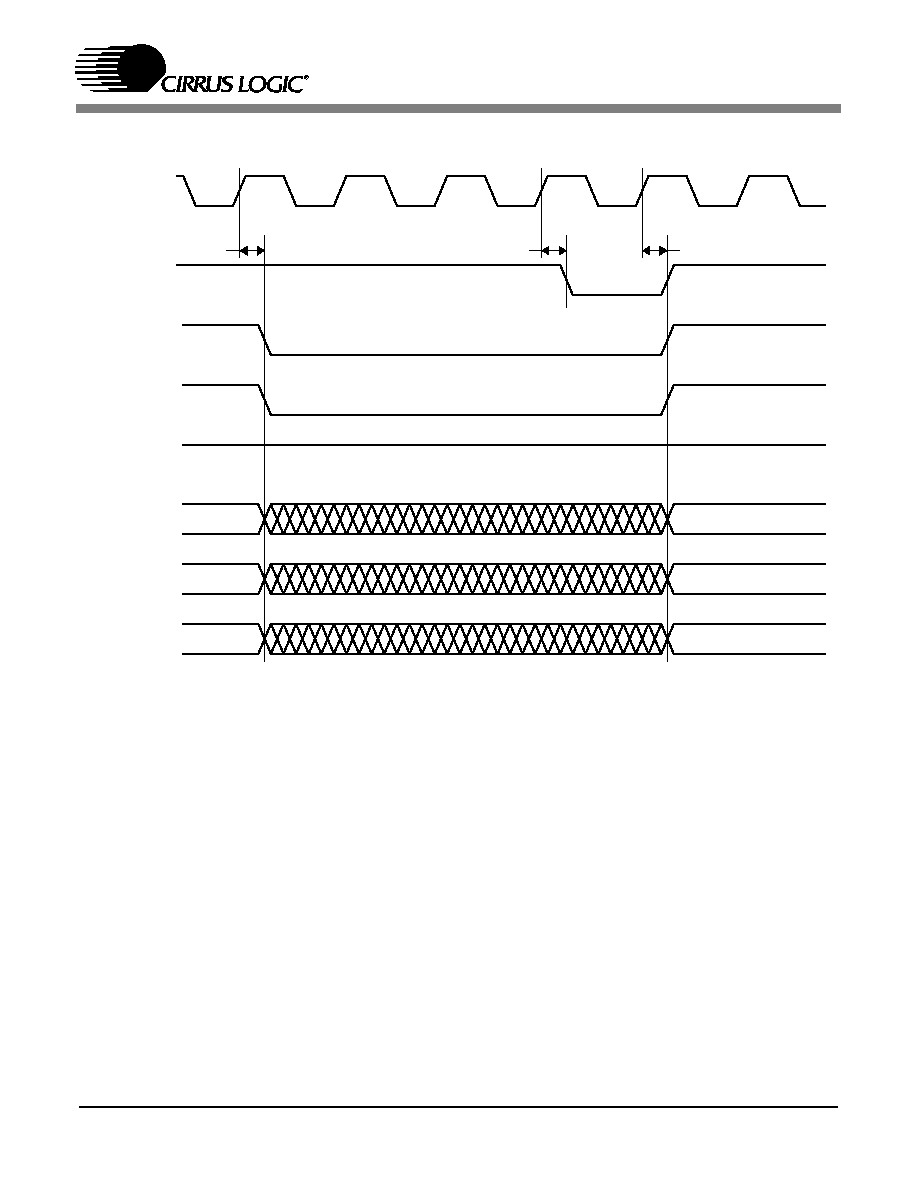
1.14 Switching Characteristics -- Digital Audio Input (DSPAB)
(T
A
= 25 ∞C; VDD, PLLVDD = 2.5 V; VDDSD = 3.3 V; C
L
= 20 pF)
Notes: 1. This timing parameter is defined from the active edge of FSCLKN1/2. The active edge of FSCLKN1/2
is the point at which the data is valid.
2. Slave mode is defined as FSCLKN1/2 and FLRCLKN1/2 driven by an external source.
Parameter
Symbol
Min
Max
Unit
FSCLKN1 period for Slave mode
T
sclki
40
-
ns
FSCLKN1 duty cycle for Slave mode
45
55
%
Slave Mode
(Note 2)
Time from active edge of FSCLKN1(2) to FLRCLKN1(2) transition
T
stlr
10
-
ns
Time from FLRCLKN1(2) transition to FSCLKN1(2) active edge
T
lrts
10
-
ns
FSDATAN1(2) setup to FSCLKN1(2) transition
(Note 1)
T
sdsus
5
-
ns
FSDATAN1(2) hold time after FSCLKN1(2) transition
(Note 1)
T
sdhs
5
-
ns
T
s c lk i
T
lrts
T
s tlr
T
s ds u s
T
s d hs
F S C L K N 1
F S D A T A N 1
F L R C L K N 1
F S C L K N 2
F L R C L K N 2
F S D A T A N 2
Figure 13. Digital Audio Input Data, Slave Clock Timing
23
1.15 Switching Characteristics -- Serial Audio Input (DSPC)
(T
A
= 25 ∞C; VDD, PLLVDD = 2.5 V; VDDSD = 3.3 V; C
L
= 20 pF)
Notes: 1. Slave mode is defined as SCLKN and LRCLKN being driven by an external source.
2. This timing parameter is defined from the active edge of SCLKN. The active edge of SCLKN is the point
at which the data is valid.
Parameter
Symbol
Min
Max
Unit
Slave Mode
SCLKN period for Slave mode
T
sclki
40
-
ns
SCLKN duty cycle for Slave mode
45
55
%
Time from active edge of SCLKN to LRCLKN transition
T
stlr
20
-
ns
Time from LRCLKN transition to SCLKN active edge
T
lrts
20
-
ns
SDATAN0 setup to SCLKN transition
(Notes 2)
T
sdsus
10
-
ns
SDATAN0 hold time after SCLKN transition
(Notes 2)
T
sdhs
10
-
ns
SCLKN
T
sclki
SDATAN0, 1, 2, 3
LRCLKN
T
lrts
T
stlr
T
sdsus
T
sdhs
Figure 14. Serial Audio Input Data, Slave Clock Timing

24
1.16 Switching Characteristics -- CMPDAT, CMPCLK (DSPAB)
(T
A
= 25 ∞C; VDD, PLLVDD = 2.5 V; VDDSD = 3.3 V; C
L
= 20 pF)
Parameter
Symbol
Min
Max
Unit
Serial compressed data clock CMPCLK frequency
T
cmpclk
-
27
MHz
CMPDAT setup before CMPCLK high
T
cmpsu
10
-
ns
CMPDAT hold after CMPCLK high
T
cmphld
10
-
ns
CMPCLK
T
cmpsu
T
cmpclk
CMPDAT
T
cmphld
Figure 15. Serial Compressed Data Timing
25
1.17 Switching Characteristics -- Parallel Data Input (DSPAB)
(T
A
= 25 ∞C; VDD, PLLVDD = 2.5 V; VDDSD = 3.3 V; C
L
= 20 pF)
Notes: 1. Certain timing parameters are normalized to the DSP clock, DCLK, in nanoseconds. The DSP clock can
be defined as follows:
Internal Clock Mode:
DCLK ~ 60MHz before and during boot, i.e. DCLKP ~ 16.6ns
DCLK ~ 86 MHz after boot, i.e. DCLKP ~ 11.6ns
It should be noted that DCLK for the internal clock mode is application specific. The application code
users guide should be checked to confirm DCLK for the particular application.
Parameter
Symbol
Min
Max
Unit
CMPCLK Period
T
cmpclk
4*DCLKP + 10
ns
FDAT[7:0] setup before CMPCLK high
T
cmpsu
10
ns
FDAT[7:0] hold after CMPCLK high
T
cmphld
10
ns
C MPC LK
T
cm psu
T
cm pclk
FD AT[7:0]
T
cm phld
Figure 16. Parallel Data Timing

26
1.18 Switching Characteristics -- Digital Audio Output
(T
A
= 25 ∞C; VDD, PLLVDD = 2.5 V; VDDSD = 3.3 V; C
L
= 20 pF)
Notes: 1. DSPC has two Digital Audio Output modules having analogous signal names ending in 0 and 1. Both
DAO ports share a common MCLK but have independent SCLKs and LRCLKs.
2. Master mode timing specifications are characterized, not production tested.
3. Master mode is defined as the CS49400 driving both SCLK0, SCLK1, LRCLK0, and LRCLK1. When
MCLK is an input, it is divided to produce SCLK0, SCLK1, LRCLK0 and LRCLK1.
4. This timing parameter is defined from the non-active edge of SCLK0 and SCLK1. The active edge of
SCLK0 and SCLK1 is the point at which the data is valid.
5. Slave mode is defined as SCLK0, SCLK1, LRCLK0 and LRCLK1 driven by an external source.
Parameter
Symbol
Min
Max
Unit
MCLK period
T
mclk
40
-
ns
MCLK duty cycle
40
60
%
SCLK0, SCLK1 period for Master or Slave mode
(Note 2)
T
sclk
40
-
ns
SCLK0, SCLK1 duty cycle for Master or Slave mode
(Note 2)
45
55
%
Master Mode (Output A1 Mode)
(Note 2, 3)
SCLK0, SCLK1 delay from MCLK rising edge, MCLK as an
input
T
sdmi
15
ns
LRCLK0, LRCLK1 delay from SCLK0, SCLK1 transition,
respectively
(Note 4)
T
lrds
10
ns
AUDATA7≠0 delay from SCLK0, SCLK1 transition
(Note 4)
T
adsm
10
ns
Slave Mode (Output A0 Mode)
(Note 5)
Time from active edge of SCLK0, SCLK1 to LRCLK0, LRCLK1
transition
T
stlr
10
-
ns
Time from LRCLK0, LRCLK1 transition to SCLK0, SCLK1
active edge
T
lrts
10
-
ns
AUDATA7≠0 delay from SCLK0, SCLK1 transition
(Note 4)
T
adss
15
ns

27
Figure 18. Digital Audio Output Data, Input and Output Clock Timing
SCLK0,1 (Output)
MCLK (Input)
T
sdmo,
T
mclk
SCLK 0,1
(Output)
T
sclk
AUDATA7:0
LRCLK 0,1
(Output)
T
lrds
T
adsm
Master Mode (Output A1) Output Clock Timing and Digital Audio
Output Data
SCLK 0,1
(Input)
T
sclk
AUDATA7:0
LRCLK 0,1
(Input)
T
stlr
T
lrts
T
adss
Slave Mode (Output A0) Output Clock Timing and Digital Audio
Output Data
T
sdmi

28
1.19 Switching Characteristics -- SRAM/FLASH Interface
(T
A
= 25 ∞C; VDD, PLLVDD = 2.5 V; VDDSD = 3.3 V; C
L
= 20 pF)
Figure 19. SRAM/Flash Controller Timing Diagram - Write Cycle
Figure 20. SRAM/Flash Controller Timing Diagram - Read Cycle
Parameter
Symbol
Min
Max
Unit
Write Cycle
Single Byte Write Cycle
T
wrc
(SRAM_FLASH_WR_CYCLE + 1) * DCLKP
-
ns
Data Hold after NV_WE or NV_CS high
T
dh
DCLKP-5
-
ns
Data Valid after NV_CS and NV_WE low
T
dv
10
ns
Data Strobe
T
ds
DCLKP-5
-
ns
Read Cycle
Single Byte Read Cycle
T
rdc
(SRAM_FLASH_RD_CYCLE + 1) * DCLKP
-
ns
Data Strobe
T
ds
DCLKP-5
-
ns
Data Hold after NV_WE or NV_CS high
T
dh
DCLKP+5
-
ns
Data Setup Time
T
su
DCLKP+5
-
ns
XTA[19:0]
NV_CS
NV_WE
XTD[7:0]
T
wrc
T
dh
T
ds
T
dv
MSP
LSP
EXTA[19:0]
NV_CS
NV_OE
EXTD[7:0]
T
rdc
T
dh
T
ds
T
su
MSP
LSP

29
Figure 21. SRAM/Flash Controller Timing Diagram - Single Byte Write Cycle
Figure 22. SRAM/Flash Controller Timing Diagram - Single Byte Read Cycle
EXTA[19:0]
NV_CS
NV_WE
EXTD[7:0]
T
wrc
T
dh
T
ds
T
dv
LSP
NV_OE
Valid
EXTA[19:0]
NV_CS
NV_OE
EXTD[7:0]
T
rdc
T
dh
T
ds
T
su
LSP
NV_WE
Valid

30
1.20 Switching Characteristics -- SDRAM Interface
(T
A
= 25 ∞C; VDD, PLLVDD = 2.5 V; VDDSD = 3.3 V; C
L
= 20 pF, SD_CLKOUT = SD_CLKIN)
Figure 23. SDRAM Controller Timing Diagram - Load Mode Register Cycle
Parameter
Symbol
Min
Max
Unit
SD_CLKIN high time
t
clk_high
0.475*DCLKP
-
ns
SD_CLKIN low time
t
clk_low
0.475*DCLKP
-
ns
SD_CLKOUT rise/fall time
t
clkrf
-
1
ns
SD_CLKOUT duty cycle
t
clkrf
45
55
%
SD_CLKOUT rising edge to signal valid
t
d
-
9.8
ns
Signal hold from SD_CLKOUT rising edge
t
h
1.0
ns
SD_CLKOUT rising edge to SD_DQMn valid
t
DQd
-
7.2
ns
SD_DQMn hold from SD_CLKOUT rising edge
t
DQh
1.0
-
ns
SD_DATA valid setup to SD_CLKIN rising edge
t
DAs
8.3
ns
SD_DATA valid hold to SD_CLKIN rising edge
t
DAh
1.0
ns
SD_CLKOUT rising edge to ADDRn valid
t
d
-
8.0
ns
SD _CL K O UT
S
S
S
S D
D
D
D _
_
_
_C
C
C
C S
S
S
S
S
S
S
S D
D
D
D _
_
_
_R
R
R
R A
A
A
A S
S
S
S
S
S
S
S D
D
D
D _
_
_
_C
C
C
C A
A
A
A S
S
S
S
S
S
S
S D
D
D
D _
_
_
_W
W
W
W E
E
E
E
SD _DQ M n
S D_ AD D Rn
S D_ DA TA n
O P CO D E
t
d
t
h
31
L
KO
UT
S
S
S
S
D
D
D
D_
_
_
_C
C
C
CS
S
S
S
D
D
D
D
_
_
_
_R
R
R
RA
A
A
AS
S
S
S
D
D
D
D
_
_
_
_C
C
C
CA
A
A
AS
S
S
S
S
S
S
S
D
D
D
D_
_
_
_W
W
W
WE
E
E
E
_
DQ
M
n
A
DD
Rn
D
AT
A
n
t
d
t
h
t
DQ
h
L
S
P0
M
S
P0
00
11
F
i
gur
e
24.
S
DRAM
C
o
n
t
r
o
l
l
e
r
T
i
m
i
ng
Diagr
am
-
B
ur
s
t
W
r
ite
C
yc
le

32
_C
L
K
O
U
T
S
S
S
SD
D
D
D_
_
_
_C
C
C
CS
S
S
S
S
S
S
SD
D
D
D_
_
_
_R
R
R
RA
A
A
AS
S
S
S
S
S
S
SD
D
D
D_
_
_
_C
C
C
CA
A
A
AS
S
S
S
S
S
S
SD
D
D
D_
_
_
_W
W
W
WE
E
E
E
S
D_
DQ
M
n
D_
AD
DR
n
S
D_
DA
T
A
n
t
DA
s
t
cl
kr
f
t
d
t
d
t
DQ
d
t
h
t
DA
h
T
DQ
h
C
AS=
2
L
SP0
M
S
P0
L
SP3
M
SP3
S
D_
CL
K
I
N
t
cl
k
_
l
o
w
t
cl
k_
h
i
g
h
00
11
F
i
gur
e
25
.
S
DRAM
Contr
o
ll
e
r
T
i
m
i
ng
Di
agr
am
-
B
ur
s
t
Re
ad
Cyc
l
e
33
Figure 26. SDRAM Controller Timing Diagram - Auto Refresh Cycle
SD_CLKOUT
S
S
S
SD
D
D
D_
_
_
_C
C
C
CS
S
S
S
S
S
S
SD
D
D
D_
_
_
_R
R
R
RA
A
A
AS
S
S
S
S
S
S
SD
D
D
D_
_
_
_C
C
C
CA
A
A
AS
S
S
S
S
S
S
SD
D
D
D_
_
_
_W
W
W
WE
E
E
E
SD_DQMn
SD_ADDRn
SD_DATAn
t
d
t
h
t
d

34
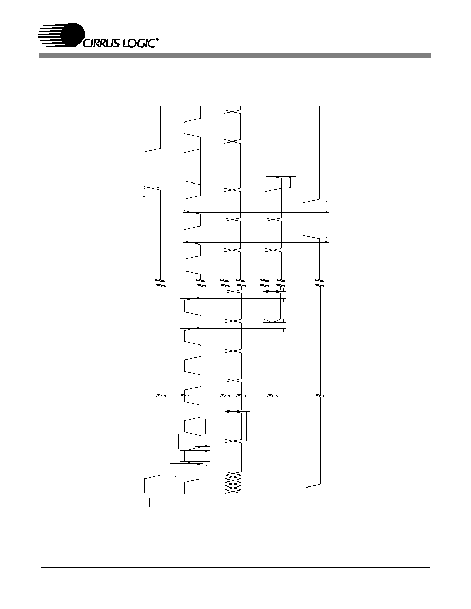
2. OVERVIEW
The CS49400 is a 24-bit fixed-point decoder DSP
followed by a 32-bit fixed point programmable
post-processor DSP. The decoder portion of the
CS49400 is referred to as "DSPAB". The post-
processor DSP is referred to as "DSPC". Both
DSPAB and DSPC include their own dedicated
peripherals such as serial and parallel control ports,
and serial audio interfaces. DSPC also has a
external
memory
interface
which
supports
SRAM/SDRAM/EPROM.
All the decoding/processing algorithms listed
below require delivery of PCM or IEC61937-
packed compressed data via I2S or LJ formatted
digital audio to the CS49400. Today the CS49400
will
support
all
of
the
following
decoding/processing standards:
∑
PCM Pass-Through/PCM Upsampler
∑
Dolby Digital
TM
(with Dolby Pro Logic)
TM
∑
Dolby Digital Pro Logic II
TM
∑
Dolby Digital EX
TM
∑
Dolby Digital EX Pro Logic II
TM
∑
MPEG-2, Advanced Audio Coding Algorithm
(AAC)
∑
MPEG Multichannel
∑
MPEG Multichannel with Dolby Pro Logic II
TM
∑
MPEG-1/2, Layer III (MP3)
∑
DTS Digital SurroundTM
∑
DTS 96/24TM (Front-end Decoder)
∑
DTS Digital SurroundTM with
Dolby Pro Logic IITM
∑
DTS-ES Extended Surround
TM
(DTS-ES Discrete 6.1 and DTS-ES Matrix 6.1)
∑
DTS-ES 96/24
TM
(Front-end Decoder)
∑
DTS Neo:6
TM
∑
LOGIC7
Æ
∑
SRS Circle Surround
TM
II
∑
HDCD
Æ
All of the above audio decoding/processing
algorithms and the associated application notes
(AN208 and their corresponding appendices) are
available through the Crystal Ware
TM
Software
Licensing Program. Please refer to AN208 for the
latest listing of application codes for DSPAB.
DSPC is unique to DSPAB in the sense that the
designer may choose to just load a standard or
enhanced application code (.ULD file) from the
Crystal Ware Software Library or if they have
access
to
the
Cirrus
Framework
DSPC
Development Kit, they may choose to build their
own application code from a variety of modules. A
DSPC application code contains all of the
necessary
post-processing
modules,
such
as
Crossbar Mixer, Pro Logic Module, Bass Manager
Module, and Audio Manager (Kernel). A module is
just a single processing module, such as Tone
Control, Parametric/Graphic EQ, or Dolby Pro
Logic matrix decoder. DSPC on the CS49400 will
support the following post-processing application
codes and/or modules:
∑
Standard Post-Processor (includes the follow-
ing modules all compiled into one .ULD file):
Downmixer module, Dualzone module, Cross-
bar Mixer module, 7.1 Channel Bass Manager
module, Audio Manager module (Volume
Control, Trim Control and Channel Remap),
and Delay module
∑
Advanced Post-Processor (includes the all of
the standard post-processing modules plus the
Tone Control module, Parametric EQ module,
Re-EQ module in all compiled into one .ULD )
∑
Dolby Pro Logic
TM
∑
Dolby Pro Logic II
TM
∑
SRS Circle Surround II
TM
∑
DTS Neo:6
TM
∑
LOGIC7
Æ
∑
THX
Æ
Surround EXTM 7.1 Channel
Post-Processor

35
∑
THX
Æ
Ultra2 Cinema
TM
7.1 Channel
Post-Processor
∑
Cirrus Extra Surround
TM
∑
Cirrus Original Multichannel Surround
TM
∑
Virtual Dolby Digital
TM
/Virtual Dolby Digital
Pro Logic II
TM
Virtualizer Module
∑
VMAx VirtualTheater
TM
Virtualizer Module
∑
HDCD
Æ
Multichannel Decoder
∑
DVD-Audio/Video and Multichannel SACD
Bass Management
∑
DTS/DTS-ES 96/24
TM
Back-End Decoder
∑
DTS/DTS-ES 96/24
TM
Back-End Decoder with
THX
Æ
Ultra2 Cinema
TM
All of the above audio post-processing applications
codes and/or Cirrus FrameworkTM modules and
the associated application notes (AN209 and the
associated appendices) are available through the
Crystal WareTM Software Licensing Program. All
standard
or
enhanced
post-processing
code
modules are only available to customers who
qualify for the Cirrus Framework
TM
CS49400
Family DSPC Programming Kit. Please refer to
AN209 for the latest listing of application codes
and Cirrus FrameworkTM modules available for
DSPC.
2.1 DSPAB
DSPAB is an enhanced version of the CS49300. It
was designed to have legacy code support for all
decoder applications developed for the CS49300. It
includes performance enhancements such as the
ability to decode AAC without the need for
external SRAM memory. DSPAB has a Digital
Audio Input (DAI) and a Compressed Data Input
(CDI) port for data delivery in either I
2
S or LJ
format. DSPAB can be controlled serially using the
SPI standard and can also be controlled via a
Parallel host control port using the Motorola
Æ
or
Intel
Æ
communication standards.
2.2 DSPC
DSPC is a 32-bit, general-purpose, fixed-point
RAM-based processor which includes on-chip
ROM tables. It has been designed with a generous
amount of on-chip program and data RAM, and has
all necessary peripherals required to support the
latest
standards
in
consumer
entertainment
products such as AV receivers and DVD-
Audio/Video players.
DSPC has on-chip data and program RAM, and
both external SDRAM and SRAM memory
interfaces. These interfaces can be used to expand
the data memory. DSPC also has its own 8-channel
digital audio input for post-processing PCM from a
Multichannel Super Audio CD (SACD) input or
DVD-Audio/Video input, via high-performance
A/Ds or from some other type of multichannel
digital input, capable of delivering 4 stereo digital
audio channels such as IEEE1394 (a.k.a. I-Link
Æ
or Firewire
Æ
). Data can be delivered to this port
using the standard audio formats (I
2
S or LJ). DSPC
can be controlled serially using the SPI standard or
via Parallel host control port using the Motorola
Æ
or Intel
Æ
standard. DSPC has a Digital Audio
output port that has eight stereo serial data outputs
for a total of 16 channels. Data can be delivered
from these outputs in serial I
2
S or LJ format. Two
of these outputs (AUDAT3, AUDAT7) can be
configured
as
a
IEC60958-format
S/PDIF
transmitter.
This document focuses on the electrical features of
the CS49400. The features are described from a
hardware
design
perspective.
It
should
be
understood that not all of the features portrayed in
this document are supported by all of the versions
of application code available. The application code
user's guides should be consulted to determine
which hardware features are supported by the
software.
Please note that a download of application software
is required each time the part is powered up. This
term should be interpreted as meaning the transfer of
application code into the internal memory of the part
36
from either an external microcontroller or through
one of the boot procedures listed in Section 8.
3. TYPICAL CONNECTION DIAGRAMS
Four typical connection diagrams have been
presented to illustrate using the part with the
different communication modes available. They
are as follows:
Figure 27, "SPI Control with External Memory -
144 Pin Package" on page 38.
Figure 28, "Intel
Æ
Parallel Control Mode - 144 Pin
Package" on page 39.
Figure 29, "Motorola
Æ
Parallel Control Mode - 144
Pin Package" on page 40.
The following should be noted when viewing the
typical connection diagrams:
Note:
The pins are grouped functionally in each
of the typical connection diagrams. Please be
aware that the CS49400 symbol may appear
differently in each diagram.
The external memory interface is supported
when a serial or parallel communication mode
has been chosen.
3.1 Multiplexed Pins
The CS49400 incorporates a large amount of
flexibility into a 144 pin package. The pins are
internally multiplexed to serve multiple purposes.
Some pins are designed to operate in one mode at
power up, and serve a different purpose when the
DSP is running. Other pins have functionality
which can be controlled by the application running
on the DSP. In order to better explain the behavior
of the part, the pins which are multiplexed have
been given multiple names. Each name is specific
to the pin's operation in a particular mode.
In this document, pins will be referred to by their
functionality.
Section 12
"Pin Description" on
page 86
describes each pin of the CS49400 and lists
all of its names. Please refer to this section when
exact pin numbers are in question.
3.2 Termination Requirements
The CS49400 incorporates open drain pins which
must be pulled high for proper operation.
FINTREQ and INTREQ are always open drains
which requires a pull-up for proper operation.
Due to the internal, multiplexed design of the pins,
certain signals may or may not require termination
depending on the mode being used. If a parallel
host communication mode is not being used, all
parallel control pins must be terminated or driven
as these pins will come up as high impedance
inputs and will be prone to oscillation if they are
left floating. The specific termination requirements
may vary since the state of some of the GPIO pins
will determine the communication mode at the
rising edge of reset (please see
Section 6 "Control"
on page 41
for more information). For the explicit
termination requirements of each communication
mode please see the typical connection diagrams.
Generally a 3.3k Ohm resistor is recommended for
open drain and mode select pins. A 10k Ohm
resistor is sufficient for all other unused inputs.
3.3 Phase Locked Loop Filter
The internal phase locked loop (PLL) of the
CS49400 requires an external filter. The topology
of this filter is shown in the typical connection
diagrams. The component values are shown below.
Care should be taken when laying out the filter
circuitry to minimize trace lengths and to avoid any
high frequency signals. Any noise coupled onto the
filter circuit will be directly coupled into the PLL,
which could affect performance.
Reference Designator
Value
C1
2.2uF
C2
1200pF
C3
68pF
R1
3k Ohm
Table 1. PLL Filter Component Values

37
4. POWER
The CS49400 requires a 2.5V digital power supply
for the core logic and 2.5V I/O and a 2.5V analog
power supply for the internal PLL. For systems
with external memory that runs on 3.3V, a 3.3V
digital power supply is required on the VDDSD
pins along with four digital grounds on VSSSD.
There are seven digital power pins, VDD1 through
VDD7, along with seven digital grounds, VSS1
through VSS7. There is one analog power pin,
PLLVDD, and one analog ground, PLLVSS. The
recommendations given below for decoupling and
power conditioning of the CS49400 will help to
ensure reliable performance.
4.1 Decoupling
It is necessary to decouple the power supply by
placing capacitors directly between the power and
ground of the CS49400. Each pair of power/ground
pins (VDD1/VSS1, etc.) should have its own
decoupling
capacitors.
The
recommended
procedure is to place both a 0.1uF and a 1uF
capacitor as close as physically possible to each
power pin. The 0.1uF capacitor should be closest to
the part (typically 5mm or closer).
4.2 Analog Power Conditioning
In order to obtain the best performance from the
CS49400's internal PLL, the analog power supply
PLLVDD must be as noise-free as possible. A
ferrite bead and two capacitors should be used to
filter the VDD to generate PLLVDD. This power
scheme is shown in the typical connection
diagrams.
4.3 Ground
For two layer circuit boards, care should be taken
to have sufficient ground between the DSP and
parts in which it will be interfacing (DACs, ADCs,
S/PDIF Receivers, microcontrollers, and especially
external memory). Insufficient ground can degrade
noise margins between devices resulting in data
integrity problems.
4.4 Pads
The CS49400 has two different I/O voltage levels.
All signal pins not associated with the External
SRAM/SDRAM memory interface operate from
the 2.5V supply and are 3.3V tolerant. The external
SRAM/SDRAM memory interface operates at
3.3V only. However, if the external memory
interface is not used VDDSD1-4 may be connected
to 2.5V.
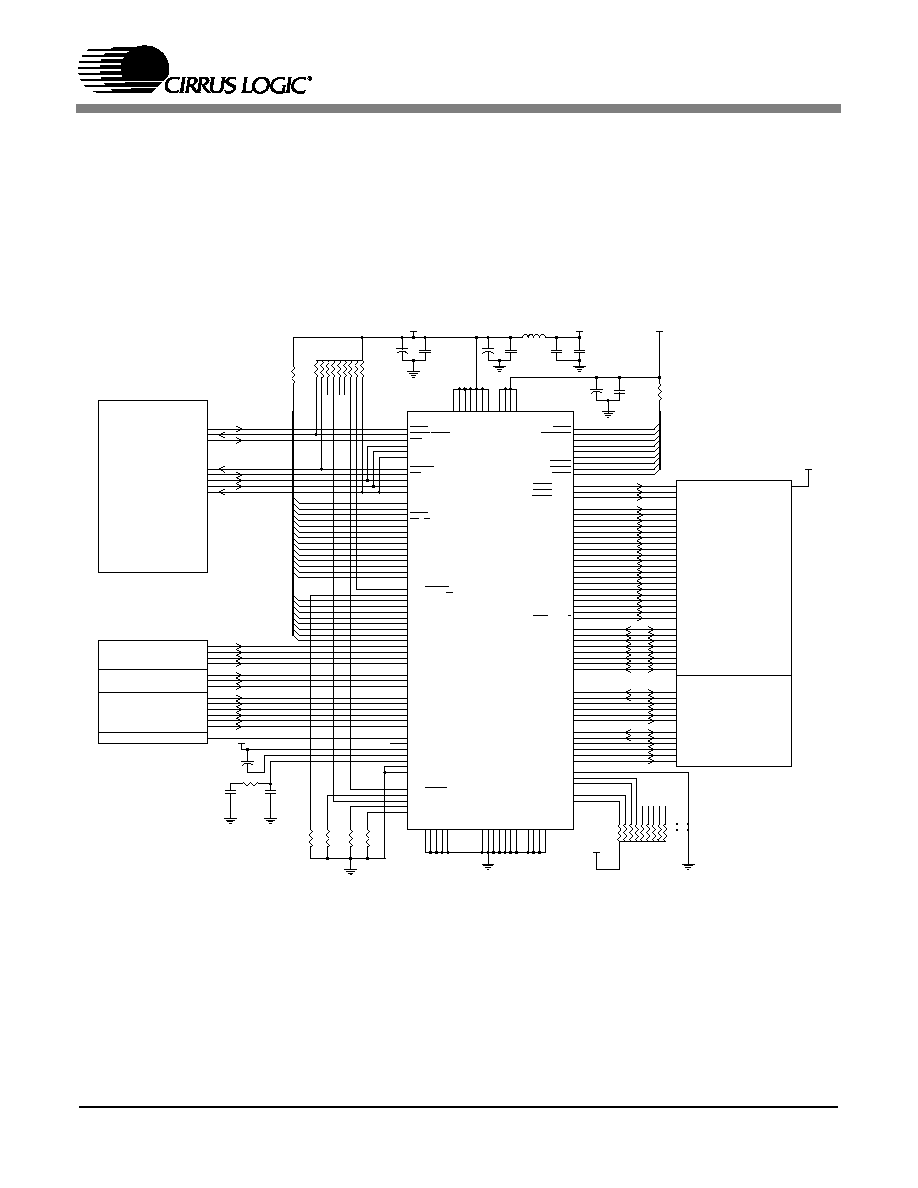
38
2 SPDIF TX
6 DACs
SPI
INTERFACE
ADC OR SPDIF RX
RESISTOR PACK.
EXTERNAL ROM
ADC
MICROCONTROLLER
ADCs
OSCILLATOR
RESISTOR PACK.
NOTE:
1. A capacitor pair (.01uF and 0.1uF) must
be supplied for each power pin.
2. The digital supply (+2.5 VD) is filtered.
to obtain the analog suply (+2.5 VA).
+2.5 VD
+2.5 VD
+2.5 VA
+3.3VD
+2.5 VA
+3.3VD
C3
0.1uF
10K
3.3K
+
1uF
FERRITE BEAD
10K
10K
C
3.3K
1
2
3
4
5
6
7
8
9
10
+
C1
0.1uF
10K
C
3.3K
1
2
3
4
5
6
7
8
9
10
C2
47uF
0.1uF
3.3K
0.01uF
+
1uF
R1
CS494XX
69
39
137
72
53
42
115
126
141
98
35
103
83
75
105
32
86
1
59
33
85
93
62
56
144
22
27
36
23
17
96
101
74
116
12
34
41
125
94
136
81
113
134
110
87
44
107
77
47
61
132
15
20
25
121
2
10
78
91
5
119
122
102
71
67
38
142
52
138
130
99
97
82
55
70
58
120
123
8
28
30
49
13
92
18
108
64
84
3
80
117
37
104
43
73
40
114
46
140
7
111
135
31
76
57
106
128
60
26
21
133
16
63
139
11
109
6
95
90
89
88
66
112
45
131
51
48
127
143
100
54
50
14
124
19
24
29
79
4
9
65
129
118
68
VSSSD1
SD_DQM0
VSS5
SD_ADR10,EXTA10
SD_DATA11,EXTA14
VDDSD4
HDATA1,GPIO1
CLKOUT,XTAL0
HINBSY,GPIO8
SCLK1
SD_DAT1,EXTD1
HDATA4,GPIO4
NC4
SD_ADDR2,EXTA2
HDATA3,GPIO3
NV_CS,GPIO14
SCLKN,GPIO22
UHS0,GPIO18
SD_CLK_OUT
SD_WE
LRCLKN, GPIO23
AUDATA6,GPIO30
SD_ADDR8, EXTA8
SD_DATA8,EXTA11
RESET
FDAT3
FDAT1
SD_DAT2, EXTD2
FDBDA
FDBCK
HDATA6,GPIO6
VSS2
SD_ADDR1, EXTA1
HDATA0,GPIO0
FHS0,FWR,FDS
SD_DAT0,EXTD0
VSSSD4
PLLVDD
AUDATA5,GPIO29
SCDIN
SDATAN1,GPIO25
VSS3
FSCLKN1,STCCLK2
AUDATA0
LRCLK1
SD_DATA7,EXTD7
AUDATA2
SD_RAS
SD_DATA14,EXTA17
SD_CLK_IN
VDD4
FCS
VDD7
DBDA
RD,R/W,GPIO11
UHS1,GPIO19
VDD6
SD_CAS
VSS1
GPIO20
FLRCLKN1
PLLVSS
AUDATA4,GPIO28
SD_BA,EXTA19
SD_ADDR4,EXTA4
SD_DATA4,EXTD4
SCCLK
SD_DATA12, EXTA15
VDD5
AO,GPIO13
MCLK
HDATA5, GPIO5
SDATAN0,GPIO24
SD_DATA9,EXTA12
VDDSD1
VDDSD2
WR,DS,GPIO10
FILT2
GPIO21
TEST
NV_WE,GPIO16
SD_DATA13,EXTA16
FHS1,FRD,FR/ W
AUDATA7,XMT958B,GPIO31
FDAT5
LRCLK0
SD_CLK_EN
NC3
INTREQ,ABOOT
SDATAN2,GPIO26
CMPREQ,FLRCLKN2
SD_DATA3, EXTD3
SCLK0
SD_DATA6,EXTD6
SD_ADDR0, EXTA0
SD_DATA5,EXTD5
VDD3
SD_DATA15,EXTA18
SCDOUT,SCDIO
FHS2,FSCDIO,FSCDOUT
CMPCLK,FSCLKN2
SCS
NV_OE,GPIO15
SD_ADDR3,EXTA3
VSSSD2
AUDAT3,XMT958A
CLKSEL
SD_ADDR9,EXTA9
DBCK
VSS7
VSS4
FINTREQ
SD_ADDR7,EXTA7
A1,GPIO12
VSS6
AUDATA1
FAO,FSCCLK
HDATA7,GPIO7
VDD1
NC1
NC2
SD_ADDR5,EXTA5
HDATA2,GPIO2
SD_DQM1
FSDATAN1
VDDSD3
NC5
CLKIN,XTALI
USH2,CS_OUT,GPIO17
VDD2
SD_DATA10,EXTA13
VSSSD3
FDAT6
FILT1
FDAT4
FDAT2
FDAT0
SDATAN3,GPIO27
FA1, FSCDIN
FDAT7
SD_ADDR6,EXTA6
CS,GPIO9
CMPDAT,FSDATAN2
SD_CS
0.1uF
Figure 27. SPI Control with External Memory - 144 Pin Package

39
OSCILLATOR
2 SPDIF TX
MICROCONTROLLER
6 DACs
ADC OR SPDIF RX
EXTERNAL ROM
ADC
NOTE:
1. A capacitor pair (.01uF and 0.1uF) must
be supplied for each power pin.
2. The digital supply (+2.5 VD) is filtered.
to obtain the analog suply (+2.5 VA).
PARALLEL
INTERFACE
ADCs
+2.5 VA
+2.5 VA
+3.3VD
+2.5 VD
+2.5 VD
+3.3VD
CS494XX
69
39
137
72
53
42
115
126
141
98
35
103
83
75
105
32
86
1
59
33
85
93
62
56
144
22
27
36
23
17
96
101
74
116
12
34
41
125
94
136
81
113
134
110
87
44
107
77
47
61
132
15
20
25
121
2
10
78
91
5
119
122
102
71
67
38
142
52
138
130
99
97
82
55
70
58
120
123
8
28
30
49
13
92
18
108
64
84
3
80
117
37
104
43
73
40
114
46
140
7
111
135
31
76
57
106
128
60
26
21
133
16
63
139
11
109
6
95
90
89
88
66
112
45
131
51
48
127
143
100
54
50
14
124
19
24
29
79
4
9
65
129
118
68
VSSSD1
SD_DQM0
VSS5
SD_ADR10,EXTA10
SD_DATA11,EXTA14
VDDSD4
HDATA1,GPIO1
CLKOUT,XTAL0
HINBSY,GPIO8
SCLK1
SD_DAT1,EXTD1
HDATA4,GPIO4
NC4
SD_ADDR2,EXTA2
HDATA3,GPIO3
NV_CS,GPIO14
SCLKN,GPIO22
UHS0,GPIO18
SD_CLK_OUT
SD_WE
LRCLKN,GPIO23
AUDATA6,GPIO30
SD_ADDR8, EXTA8
SD_DATA8,EXTA11
RESET
FDAT3
FDAT1
SD_DAT2, EXTD2
FDBDA
FDBCK
HDATA6,GPIO6
VSS2
SD_ADDR1, EXTA1
HDATA0,GPIO0
FHS0,FWR,FDS
SD_DAT0,EXTD0
VSSSD4
PLLVDD
AUDATA5,GPIO29
SCDIN
SDATAN1,GPIO25
VSS3
FSCLKN1,STCCLK2
AUDATA0
LRCLK1
SD_DATA7,EXTD7
AUDATA2
SD_RAS
SD_DATA14,EXTA17
SD_CLK_IN
VDD4
FCS
VDD7
DBDA
RD,R/W,GPIO11
UHS1,GPIO19
VDD6
SD_CAS
VSS1
GPIO20
FLRCLKN1
PLLVSS
AUDATA4,GPIO28
SD_BA,EXTA19
SD_ADDR4,EXTA4
SD_DATA4,EXTD4
SCCLK
SD_DATA12, EXTA15
VDD5
AO,GPIO13
MCLK
HDATA5,GPIO5
SDATAN0,GPIO24
SD_DATA9,EXTA12
VDDSD1
VDDSD2
WR,DS,GPIO10
FILT2
GPIO21
TEST
NV_WE,GPIO16
SD_DATA13,EXTA16
FHS1,FRD,FR/ W
AUDATA7,XMT958B,GPIO31
FDAT5
LRCLK0
SD_CLK_EN
NC3
INTREQ,ABOOT
SDATAN2,GPIO26
CMPREQ,FLRCLKN2
SD_DATA3, EXTD3
SCLK0
SD_DATA6,EXTD6
SD_ADDR0, EXTA0
SD_DATA5,EXTD5
VDD3
SD_DATA15,EXTA18
SCDOUT,SCDIO
FHS2,FSCDIO,FSCDOUT
CMPCLK,FSCLKN2
SCS
NV_OE,GPIO15
SD_ADDR3,EXTA3
VSSSD2
AUDAT3,XMT958A
CLKSEL
SD_ADDR9,EXTA9
DBCK
VSS7
VSS4
FINTREQ
SD_ADDR7,EXTA7
A1,GPIO12
VSS6
AUDATA1
FAO,FSCCLK
HDATA7,GPIO7
VDD1
NC1
NC2
SD_ADDR5,EXTA5
HDATA2,GPIO2
SD_DQM1
FSDATAN1
VDDSD3
NC5
CLKIN,XTALI
USH2,CS_OUT,GPIO17
VDD2
SD_DATA10,EXTA13
VSSSD3
FDAT6
FILT1
FDAT4
FDAT2
FDAT0
SDATAN3,GPIO27
FA1, FSCDIN
FDAT7
SD_ADDR6,EXTA6
CS,GPIO9
CMPDAT,FSDATAN2
SD_CS
C2
0.1uF
0.01uF
3.3K
0.1uF
3.3K
3.3K
R1
+
1uF
10K
+
C1
10K
+
1uF
0.1uF
47uF
C3
0.1uF
C
3.3K
1
2
3
4
5
6
7
8
9
10
FERRITE BEAD
C
3.3K
1
2
3
4
5
6
7
8
9
10
10K
Figure 28. Intel
Æ
Parallel Control Mode - 144 Pin Package

40
ADC OR SPDIF RX
OSCILLATOR
PARALLEL
INTERFACE
6 DACs
ADC
MICROCONTROLLER
2 SPDIF TX
ADCs
EXTERNAL ROM
RESISTOR PACK.
NOTE:
1. A capacitor pair (.01uF and 0.1uF) must
be supplied for each power pin.
2. The digital supply (+2.5 VD) is filtered.
to obtain the analog suply (+2.5 VA).
+2.5 VA
+2.5 VD
+2.5 VD
+3.3VD
+2.5 VA
+3.3VD
47uF
0.1uF
10K
CS494XX
69
39
137
72
53
42
115
126
141
98
35
103
83
75
105
32
86
1
59
33
85
93
62
56
144
22
27
36
23
17
96
101
74
116
12
34
41
125
94
136
81
113
134
110
87
44
107
77
47
61
132
15
20
25
121
2
10
78
91
5
119
122
102
71
67
38
142
52
138
130
99
97
82
55
70
58
120
123
8
28
30
49
13
92
18
108
64
84
3
80
117
37
104
43
73
40
114
46
140
7
111
135
31
76
57
106
128
60
26
21
133
16
63
139
11
109
6
95
90
89
88
66
112
45
131
51
48
127
143
100
54
50
14
124
19
24
29
79
4
9
65
129
118
68
VSSSD1
SD_DQM0
VSS5
SD_ADR10,EXTA10
SD_DATA11,EXTA14
VDDSD4
HDATA1,GPIO1
CLKOUT,XTAL0
HINBSY,GPIO8
SCLK1
SD_DAT1,EXTD1
HDATA4,GPIO4
NC4
SD_ADDR2,EXTA2
HDATA3,GPIO3
NV_CS,GPIO14
SCLKN,GPIO22
UHS0,GPIO18
SD_CLK_OUT
SD_WE
LRCLKN,GPIO23
AUDATA6,GPIO30
SD_ADDR8, EXTA8
SD_DATA8,EXTA11
RESET
FDAT3
FDAT1
SD_DAT2, EXTD2
FDBDA
FDBCK
HDATA6,GPIO6
VSS2
SD_ADDR1, EXTA1
HDATA0,GPIO0
FHS0,FWR,FDS
SD_DAT0,EXTD0
VSSSD4
PLLVDD
AUDATA5,GPIO29
SCDIN
SDATAN1,GPIO25
VSS3
FSCLKN1,STCCLK2
AUDATA0
LRCLK1
SD_DATA7,EXTD7
AUDATA2
SD_RAS
SD_DATA14,EXTA17
SD_CLK_IN
VDD4
FCS
VDD7
DBDA
RD,R/W,GPIO11
UHS1,GPIO19
VDD6
SD_CAS
VSS1
GPIO20
FLRCLKN1
PLLVSS
AUDATA4,GPIO28
SD_BA,EXTA19
SD_ADDR4,EXTA4
SD_DATA4,EXTD4
SCCLK
SD_DATA12, EXTA15
VDD5
AO,GPIO13
MCLK
HDATA5,GPIO5
SDATAN0,GPIO24
SD_DATA9,EXTA12
VDDSD1
VDDSD2
WR,DS,GPIO10
FILT2
GPIO21
TEST
NV_WE,GPIO16
SD_DATA13,EXTA16
FHS1,FRD,FR/ W
AUDATA7,XMT958B,GPIO31
FDAT5
LRCLK0
SD_CLK_EN
NC3
INTREQ,ABOOT
SDATAN2,GPIO26
CMPREQ,FLRCLKN2
SD_DATA3, EXTD3
SCLK0
SD_DATA6,EXTD6
SD_ADDR0, EXTA0
SD_DATA5,EXTD5
VDD3
SD_DATA15,EXTA18
SCDOUT,SCDIO
FHS2,FSCDIO,FSCDOUT
CMPCLK,FSCLKN2
SCS
NV_OE,GPIO15
SD_ADDR3,EXTA3
VSSSD2
AUDAT3,XMT958A
CLKSEL
SD_ADDR9,EXTA9
DBCK
VSS7
VSS4
FINTREQ
SD_ADDR7,EXTA7
A1,GPIO12
VSS6
AUDATA1
FAO,FSCCLK
HDATA7,GPIO7
VDD1
NC1
NC2
SD_ADDR5,EXTA5
HDATA2,GPIO2
SD_DQM1
FSDATAN1
VDDSD3
NC5
CLKIN,XTALI
USH2,CS_OUT,GPIO17
VDD2
SD_DATA10,EXTA13
VSSSD3
FDAT6
FILT1
FDAT4
FDAT2
FDAT0
SDATAN3,GPIO27
FA1, FSCDIN
FDAT7
SD_ADDR6,EXTA6
CS,GPIO9
CMPDAT,FSDATAN2
SD_CS
10K
10K
0.01uF
0.1uF
C
3.3K
1
2
3
4
5
6
7
8
9
10
+
1uF
0.1uF
+
1uF
0.1uF
FERRITE BEAD
R1
C3
C2
+
C1
C
10K
1
2
3
4
5
6
7
8
9
10
C
3.3K
1
2
3
4
5
6
7
8
9
10
Figure 29. Motorola
Æ
Parallel Control Mode - 144 Pin Package
41
5. CLOCKING
The CS49400 clock manager incorporates a
programmable phase locked loop (PLL) clock
synthesizer. The PLL takes an input reference
clock and produces all the clocks required to run
the DSP and peripherals.
In A/V Receiver designs, the CLKIN pin is
typically connected to a 12.288MHz oscillator.
The clock manager is controlled by the DSPAB
application software. The software user's guide for
the application code being used should be
referenced for which CLKIN input frequency is
supported.
6. CONTROL
Control of the CS49400 can be accomplished
through one of three methods. The CS49400
supports SPI serial communication and MotorolaÆ
and IntelÆ byte-wide parallel communication.
Both DSPAB and DSPC have their own control
ports. Only one of the three communication modes
can be selected for control. Both DSPAB and
DSPC use the same communication mode.
However, please note that the 100-pin package
only supports SPI serial communication. The states
of the FHS[2:0] for DSPAB and UHS[2:0] for
DSPC, sampled at the rising edge of RESET,
determine the communication interface (
Table 2.)
.
Whichever host communication mode is used, host
control of the CS49400 is handled through the
application
software
running
on
the
DSP.
Configuration and control of the CS49400 decoder
and its peripherals are indirectly executed through
a messaging protocol supported by the downloaded
application code. In other words, successful
communication can only be accomplished by
following the low level hardware communication
format and high level messaging protocol. The
specifications of the messaging protocol can be
found in any of the software user's guides, such as
AN208 and AN209.
The system designer only needs to read the
subsection describing the communication mode
being used. Please note that the communication
protocol might be slightly different for DSPAB and
DSPC.
The
following
sections
will
explain
each
communication mode in more detail. Flow
diagrams will illustrate read and write cycles.
The timing diagrams shown demonstrate relative
edge positions of signal transitions for read and
write operations.
6.1 Serial Communication
6.1.1 SPI Communication for DSPAB
SPI communication with DSPAB is accomplished
with five communication lines: chip select, serial
control clock, serial data in, serial data out, and an
interrupt request line that signals DSPAB has data
to transmit to the host.
Table 4
lists the mnemonic,
144-Pin Package
FHS2
(Pin 7)
FHS1
(Pin 13
)
FHS0
(Pin 12)
Host Interface Mode
1
0
1
Serial SPI
1
1
0
8-bit Intel
Æ
1
1
1
8-bit Motorola
Æ
100-Pin Package
FHS2
(Pin 6)
FHS1
(Pin 10
)
FHS0
(Pin 9)
Host Interface Mode
1
0
1
Serial SPI
Table 2. Host Modes for DSPAB
144-Pin Package
UHS2
(Pin 143)
UHS1
(Pin 2)
UHS0
(Pin 1)
Host Interface Mode
1
0
1
Serial SPI
1
1
0
8-bit Intel
Æ
1
1
1
8-bit Motorola
Æ
100-Pin Package
UHS2
(Pin 99)
UHS1
(Pin 2)
UHS0
(Pin 1)
Host Interface Mode
1
0
1
Serial SPI
Table 3. Host Modes for DSPC

42
pin name, and pin number of each of these signals
on DSPAB.
6.1.1.1 Writing in SPI for DSPAB
When writing to the device in SPI the same
protocol will be used whether writing a byte, a
message, or even an entire executable download
image. The examples shown in this document can
be expanded to fit any write situation.
Figure 30,
"SPI Write Flow Diagram for DSPAB" on page 42
shows a typical write sequence:
The following is a detailed description of an SPI
write sequence with DSPAB.
1) An SPI transfer is initiated when chip select
(FCS) is driven low.
2) This is followed by a 7-bit address and the
read/write bit set low for a write. The address
for DSPAB defaults to 1000000b. It is
necessary to clock this address in prior to any
transfer in order for DSPAB to accept the write.
In other words a byte of 0x80 should be clocked
into the device preceding any write. The 0x80
byte represents the 7-bit address 1000000b,
with the least significant bit set to 0 to designate
a write.
3) The host should then clock data into the device
most significant bit first, one byte at a time. The
data byte is transferred from the shift register to
the DSP input register on the falling edge of the
eighth serial clock. For this reason, the serial
clock should default to low so that eight
transitions from low to high to low will occur
for each byte. A 32
µS byte to byte latency must
be obeyed during run time.
4) When all of the bytes have been transferred,
chip select should be raised to signify an end of
write. Once again it is crucial that the serial
clock transitions from high to low on the last bit
of the last byte before chip select is raised, or a
loss of data will occur.
The same write routine could be used to send a
single byte, a message, or an entire application
code image. From a hardware perspective, it makes
no difference whether communication is by byte or
multiple bytes of any length as long as the correct
hardware protocol is followed.
6.1.1.2 Reading in SPI for DSPAB
A read operation is necessary when DSPAB signals
that it has data to be read. DSPAB does this by
dropping its interrupt request line (FINTREQ) low.
When reading from the device in SPI, the same
protocol will be used whether reading a single byte
or multiple bytes. The examples shown in this
document can be expanded to fit any read situation.
Figure 32, "SPI Read Flow Diagram for DSPAB"
on page 44
shows a typical read sequence:
The following is a detailed description of an SPI
read sequence with DSPAB.
Mnemonic
Pin Name
144-Pin
Package,
Pin
Number
100-Pin
Package,
Pin
Number
Chip Select
FCS
15
11
Serial Clock
FSCCLK
6
5
Serial Data In
FSCDIN
4
4
Serial Data Out FSCDOUT
7
6
Interrupt
Request
FINTREQ
16
12
Table 4. SPI Communication Signals for DSPAB
SPI STAR T: FC S (LO W )
W RIT E AD DRESS BYTE
W ITH M ODE BIT
SET TO 0 F OR W RITE
MOR E D ATA?
Y
N
W R IT E D ATA BY TE
SPI STO P: FC S (H IGH )
Figure 30. SPI Write Flow Diagram for DSPAB
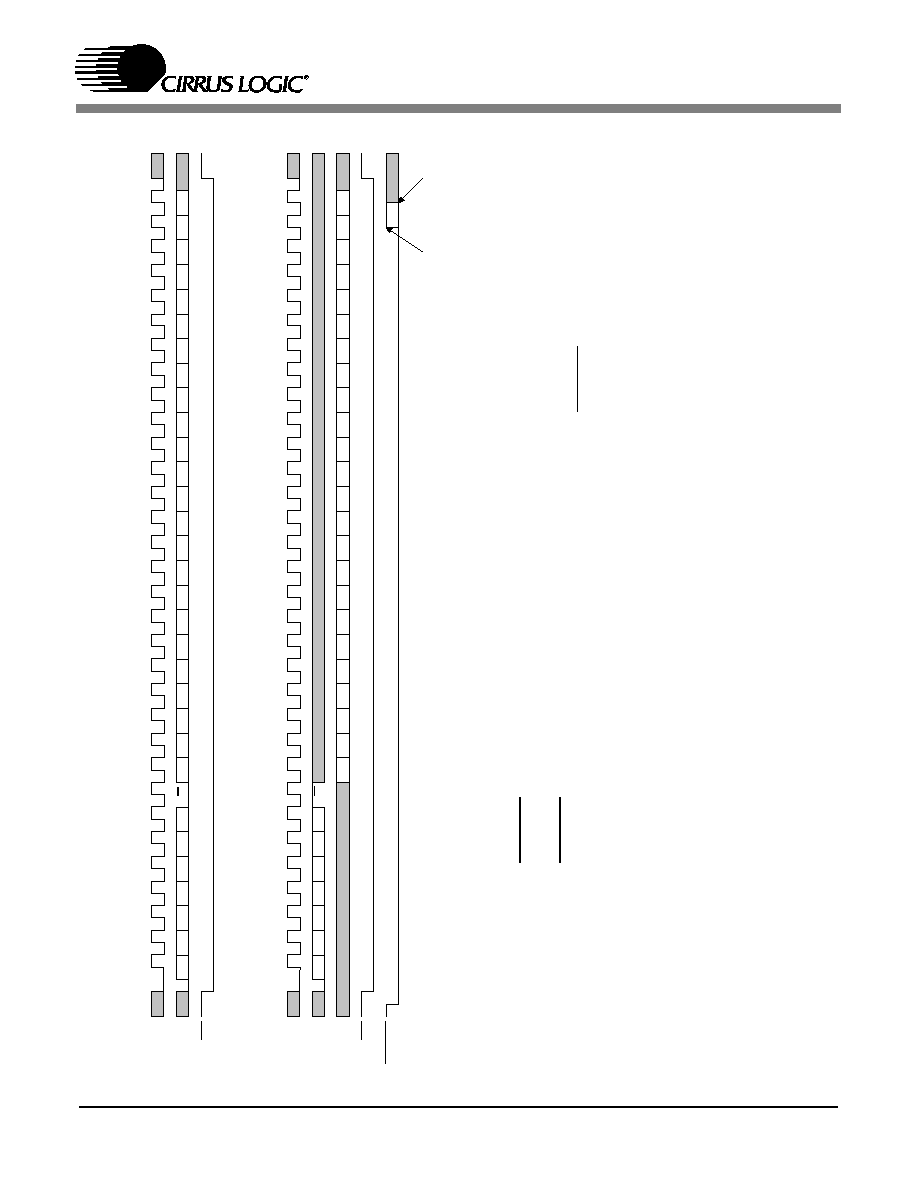
43
AD
6
A
D
4
A
D
5
A
D3
A
D
2
A
D1
A
D
0
R
/
W
D7
D
6
D5
D4
D3
D
2
D1
D
0
D7
D
6
D
5
D
4
D3
D2
D1
D0
D7
D6
D5
D4
D
3
D2
D1
D0
SC
C
L
K
S
CDIN
Not
e
1
S
P
I
W
r
i
t
e
F
u
n
c
t
i
onal
T
i
m
i
n
g
No
t
e
2
S
P
I
R
e
ad
F
u
nc
t
i
o
n
a
l
T
i
m
i
n
g
CS
AD
6
A
D
4
AD
5
A
D
3
AD
2
A
D
1
A
D
0
R
/W
D7
D6
D5
D4
D3
D2
D
1
D0
D7
D6
D
5
D4
D3
D2
D1
D0
D7
D6
D5
D4
D3
D
2
D1
D0
S
CDIN
S
CCL
K
S
CDO
UT
CS
INTR
E
Q
F
F
F
F
F
F
F
F
Fi
g
u
re
3
1
.
S
P
I
T
i
mi
n
g
f
o
r
D
S
P
A
B
Notes:
1.
F
I
NT
RE
Q
i
s
guarant
eed
t
o
s
t
a
y
L
O
W
u
n
t
i
l
t
h
e
r
i
s
i
n
g
edge
o
f
F
S
CC
LK
f
o
r
b
i
t
D1
of
t
h
e
l
as
t
b
y
t
e
t
o
be
t
r
ans
f
e
rred
out
of
t
h
e
C
S
4
9
400.
2.
F
I
NT
RE
Q
i
s
guarant
eed
t
o
rem
a
i
n
HI
GH
unt
i
l
t
h
e
nex
t
r
i
s
i
n
g
edge
of
F
S
CCLK
a
t
w
hi
c
h
p
o
i
n
t
i
t
m
a
y
g
o
L
OW
agai
n
i
f
t
he
r
e
i
s
new
dat
a
t
o
b
e
r
ea
d.
T
h
e
c
ondi
t
i
o
n
of
F
I
NT
RE
Q
go
i
n
g
L
O
W
a
t
t
h
i
s
p
o
i
n
t
s
hou
l
d
b
e
t
r
eat
ed
as
a
new
read
c
ondi
t
i
on.
A
f
t
e
r
a
s
t
op
c
ondi
t
i
o
n
,
a
new
s
t
art
c
ondi
t
i
on
an
d
a
n
add
r
e
s
s
by
t
e
s
houl
d
b
e
s
ent
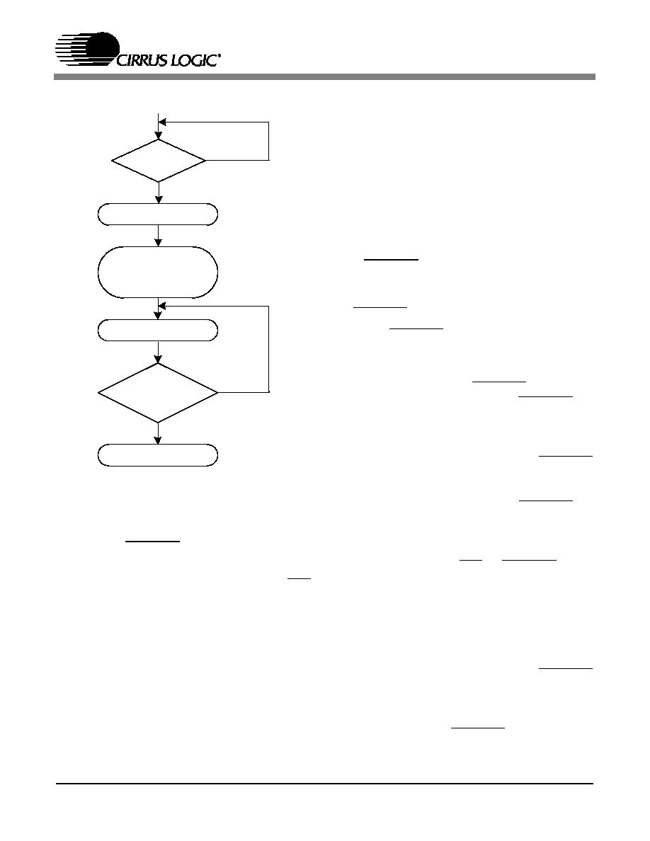
44
1) An SPI read transaction is initiated by DSPAB
dropping FINTREQ, signaling that it has data
to be read.
2) The host responds by driving chip select (FCS)
low.
3) This is followed by a 7-bit address and the
read/write bit set high for a read. The address
for DSPAB defaults to 1000000b. It is
necessary to clock this address in prior to any
transfer in order for DSPAB to acknowledge
the read. In other words a byte of 0x81 should
be clocked into the device preceding any read.
The 0x81 byte represents the 7-bit address
1000000b, and the least significant bit set to 1
to designate a read.
4) After the falling edge of the serial control clock
(FSCCLK) for the read/write bit, the data is
ready to be clocked out on the control data out
pin (FCDOUT). Data clocked out by the host is
valid on the rising edge of FSCCLK. Data
transitions occur on the falling edge of
FSCCLK. The serial clock should be default
low so that eight transitions from low to high to
low will occur for each byte.
5) If FINTREQ is still low, another byte should be
clocked out of DSPAB. Please see the
discussion below for a complete description of
FINTREQ behavior.
6) When FINTREQ is released, the chip select
line of DSPAB should be taken high to end the
read transaction.
Understanding the role of FINTREQ is important
for
successful
communication. FINTREQ
is
guaranteed to remain low (once it has gone low)
until the second to last rising edge of FSCCLK of
the last byte to be transferred out of DSPAB. If
there is no more data to be transferred, FINTREQ
will go high at this point. For SPI this is the rising
edge for the second to last bit of the last byte to be
transferred. After going high, FINTREQ is
guaranteed to stay high until the next rising edge of
FSCCLK. This end of transfer condition signals the
host to end the read transaction by clocking the last
data bit out and raising FCS. If FINTREQ is still
low after the second to last rising edge of FSCCLK,
the host should continue reading data from the
serial control port.
It should be noted that all data should be read out of
the serial control port during one transaction or a
loss of data will occur. In other words, all data
should be read out of the chip until FINTREQ
signals the last byte by going high as described
above. Please see
Section 6.1.3
"FINTREQ
Behavior: A Special Case" on page 48
for a more
detailed description of FINTREQ behavior.
FINTREQ
(LOW )?
FINTRE Q STILL
LO W ?
FCS HIGH
Y
N
FCS LOW
READ DA TA BYTE
W RITE ADD RES S BYTE
W ITH MODE BIT SET TO
1 FOR READ
Y
N
Figure 32. SPI Read Flow Diagram for DSPAB

45
Figure 31, "SPI Timing for DSPAB" on page 43
timing diagram shows the relative edges of the
control lines for an SPI read and write.
6.1.2 SPI Communication for DSPC
SPI
communication
with
the
DSPC
is
accomplished with five communication lines: chip
select, serial control clock, serial data in, serial data
out, and an interrupt request line that signals DSPC
has data to transmit to the host.
Table 5
lists the
mnemonic, pin name, and pin number of each of
these signals on DSPC.
6.1.2.1 Writing in SPI for DSPC
When writing to the device in SPI the same
protocol will be used whether writing a byte, a
message or even an entire executable download
image. The examples shown in this document can
be expanded to fit any write situation.
Figure 33,
"SPI Write Flow Diagram for DSPC" on page 45
shows a typical write sequence
The following is a detailed description of an SPI
write sequence with DSPC.
1) An SPI transfer is initiated when chip select
(SCS) is driven low.
2) This is followed by a 7-bit address and the
read/write bit set low for a write. The address
for DSPC defaults to 1000001b. It is necessary
to clock in this address prior to any transfer in
order for DSPC to accept the write. In other
words a byte of 0x82 should be clocked into the
device preceding any write. The 0x82 byte
represents the 7-bit address 1000001b, and the
least significant bit set to 0 to designate a write.
3) The host should then clock data into the device
most significant bit first, four bytes at a time.
The data byte is transferred to the DSP on the
falling edge of the eighth serial clock. For this
Mnemonic
Pin Name
144-Pin
Package,
Pin
Number
100-Pin
Package,
Pin
Number
Chip Select
SCS
135
93
Serial Clock
SCCLK
142
98
Serial Data In
SCDIN
136
94
Serial Data Out
SCDOUT
140
97
Host Busy
HINBSY
141
N/A
Interrupt
Request
INTREQ
3
3
Table 5. SPI Communication Signals for DSPC
SPI START: SCS (LOW)
WRITE ADDRESS BYTE
WITH MODE BIT
SET TO 0 FOR WRITE
MORE DATA?
Y
N
WRITE 4 DATA BYTES
SPI STOP: SCS (HIGH)
HINBSY
(HIGH)?
N
Y
Figure 33. SPI Write Flow Diagram for DSPC
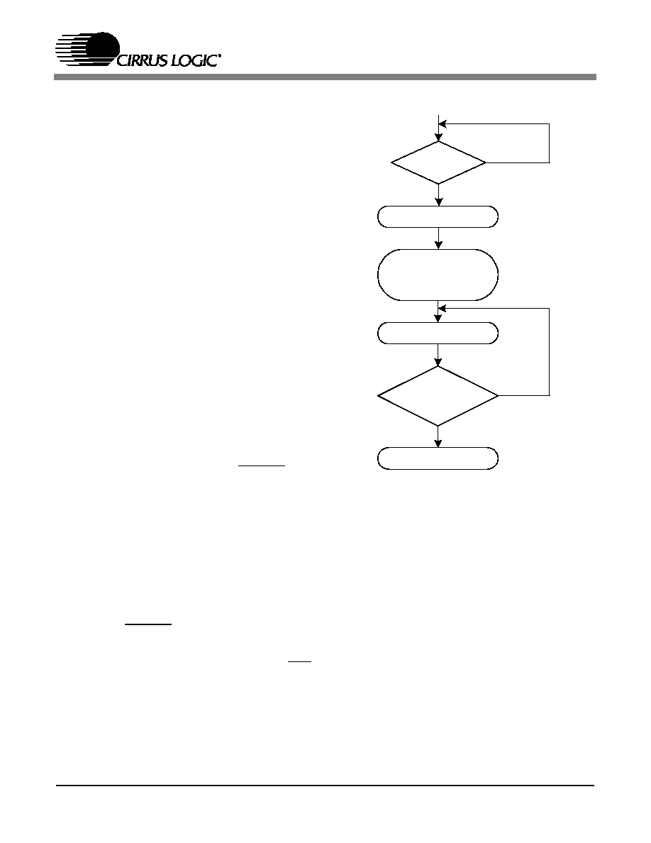
46
reason, the serial clock should default to low so
that eight transitions from low to high to low
will occur for each byte.
4) When all 4 data bytes have been transferred,
chip select should be raised to signify an end of
write. Once again it is crucial that the serial
clock transitions from high to low on the last bit
of the last byte before chip select is raised, or a
loss of data will occur.
5) If more data needs to be sent, the host must
verify that the HINBSY pin is low before it
sends more data to DSPC. Note the HINBSY
pin is available only on the 144 pin devices. A
32
µS byte to byte latency must be obeyed
during run time for the 100 pin devices.
The same write routine could be used to send a 4-
byte message or an entire application code image.
From a hardware perspective, communication must
be in 4-byte multiples.
6.1.2.2 Reading in SPI for DSPC
A read operation is necessary when DSPC signals
that it has data to be read. DSPC does this by
dropping its interrupt request line (INTREQ) low.
When reading from the device in SPI, the same
protocol will be used whether reading a single byte
or multiple bytes. The examples shown in this
document can be expanded to fit any read situation.
Figure 35, "SPI Read Flow Diagram for DSPC" on
page 46
shows a typical read sequence:
The following is a detailed description of an SPI
read sequence with DSPC.
1) An SPI read transaction is initiated by DSPC
dropping INTREQ, signaling that it has data to
be read.
2) The host responds by driving chip select (SCS)
low.
3) This is followed by a 7-bit address and the
read/write bit set high for a read. The address
for DSPC defaults to 1000001b. It is necessary
to clock this address in prior to any transfer in
order for DSPC to acknowledge the read. In
other words a byte of 0x83 should be clocked
into the device preceding any read. The 0x83
byte represents the 7 bit address 1000001b, and
the least significant bit set to 1 designates a
read.
4) After the falling edge of the serial control clock
(SCCLK) for the read/write bit, the data is
ready to be clocked out on the control data out
pin (CDOUT). Data clocked out by the host is
valid on the rising edge of SCCLK and data
transitions occur on the falling edge of SCCLK.
The serial clock should default to low so that
eight transitions from low to high to low will
occur for each byte.
INTREQ (LO W )?
INTREQ STILL LOW ?
SCS HIGH
Y
N
SCS LO W
REA D 4 DA TA BYTES
W RITE ADD RESS BYTE
W ITH MODE BIT S ET TO
1 FOR RE AD
Y
N
Figure 35. SPI Read Flow Diagram for DSPC
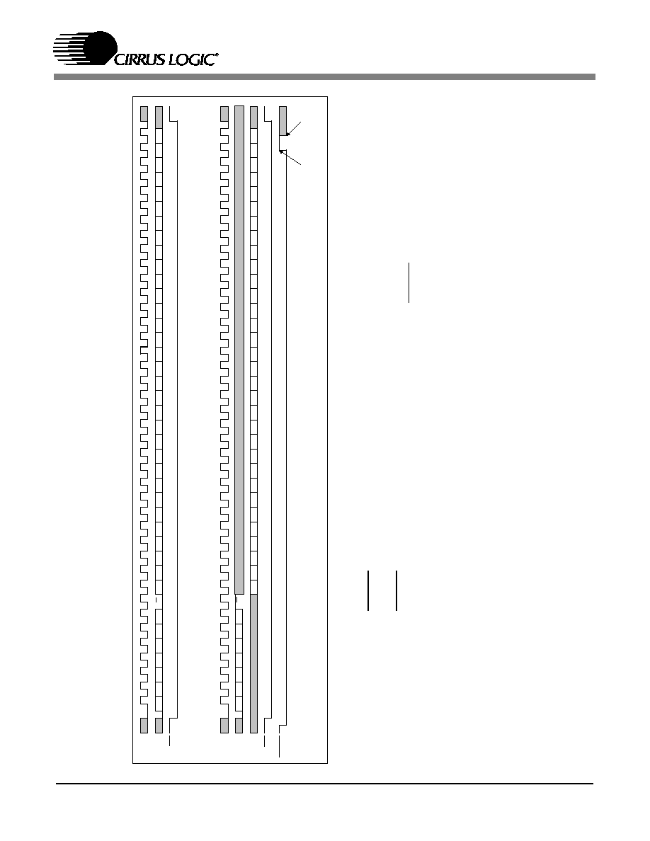
47
AD
6
A
D4
A
D
5
A
D3
A
D
2
A
D1
A
D
0
R
/
W
D7
D6
D
5
D4
D
3
D2
D
1
D0
D7
D6
D
5
D4
D3
D2
D1
D0
7D
6
D
5
D
4D
3D
2D
1D
0
SC
C
L
K
SC
D
I
N
No
t
e
1
S
P
I
W
r
i
t
e
F
u
nc
t
i
on
a
l
T
i
m
i
n
g
No
t
e
2
S
P
I
R
e
a
d
F
u
n
c
t
io
n
a
l
T
im
in
g
CS
AD
6
A
D
4
A
D
5
A
D3
AD
2
A
D1
AD
0
R/
W
D7
D6
D
5
D4
D3
D2
D1
D0
D7
D6
D5
D4
D3
D2
D1
D0
D7
D6
D5
D4
D3
D2
D1
D
0
S
CDI
N
SC
C
L
K
S
C
DO
UT
CS
IN
T
R
E
Q
S
S
D7
D6
D5
D4
D3
D2
D1
D0
D7
D6
D
5
D4
D3
D2
D1
D
0
F
i
gu
r
e
34.
S
P
I
T
im
i
n
g
f
or
DS
P
C
No
te
s:
1
.
INT
R
EQ
i
s
guarant
eed
t
o
s
t
ay
LO
W
unt
i
l
t
h
e
r
i
s
i
n
g
edge
of
S
CCL
K
f
or
bi
t
D
1
o
f
t
h
e
l
a
s
t
by
t
e
t
o
be
t
r
ans
f
e
rred
out
of
DS
P
C
.
2.
I
N
T
R
E
Q
i
s
guarant
eed
t
o
rem
a
i
n
HI
GH
unt
i
l
t
h
e
nex
t
r
i
s
i
n
g
e
dge
of
S
CCLK
a
t
w
hi
c
h
poi
nt
i
t
m
a
y
g
o
L
O
W
ag
ai
n
i
f
t
here
i
s
n
e
w
dat
a
t
o
b
e
r
ead
.
T
he
c
ondi
t
i
on
of
I
N
T
R
E
Q
go
i
n
g
L
O
W
at
t
h
i
s
poi
nt
s
houl
d
b
e
t
r
e
at
ed
as
a
new
rea
d
c
o
n
d
i
t
i
on.
A
f
t
e
r
a
s
t
op
c
ondi
t
i
on,
a
n
e
w
s
t
art
c
ondi
t
i
on
and
an
addres
s
b
y
t
e
s
houl
d
b
e
s
ent
48
5) If INTREQ is still low after 4 bytes, another 4
bytes should be clocked out of DSPC.
6) When INTREQ is released, the chip select line
of DSPC should be taken high to end the read
transaction.
All messages read back from DSPC will be in 4-
byte multiples.
6.1.3 FINTREQ Behavior: A Special Case
When communicating with DSPAB there are two
types of messages which force FINTREQ to go
low. These messages are known as solicited
messages and unsolicited messages. For more
information on the specific types of messages that
require a read from the host, one of the application
code user's guides should be referenced.
In general, when communicating with DSPAB,
FINTREQ will not go low unless the host first
sends a read request command message. In other
words the host must solicit a response from the
DSP. In this environment, the host must read from
DSPAB until FINTREQ goes high again. Once the
FINTREQ pin has gone high it will not be driven
low until the host sends another read request.
When unsolicited messages, such as those used for
Autodetect, have been enabled, the behavior of
FINTREQ is noticeably different. DSPAB will
drop the FINTREQ pin whenever it has an
outgoing message, even though the host may not
have requested data.
There are three ways in which FINTREQ can be
affected by an unsolicited message:
1) During normal operation, while FINTREQ is
high, DSPAB could drop FINTREQ to indicate an
outgoing message, without a prior read request.
2) The host is in the process of reading from
DSPAB, meaning that FINTREQ is already low.
An unsolicited message arrives which forces
FINTREQ to remain low after the solicited
message is read.
3) The host is reading from DSPAB when the
unsolicited message is queued, but FINTREQ goes
high for one period of FSCCLK and then goes low
again before the end of the read cycle.
In case (1) the host should perform a read operation
as discussed in the previous sections.
In case (2) an unsolicited message arrives before
the second to last FSCCLK of the final byte
transfer of a read, forcing the FINTREQ pin to
remain low. In this scenario the host should
continue to read from DSPAB without a stop/start
condition or data will be lost.
In case (3) an unsolicited message arrives between
the second to last FSCCLK and the last FSCCLK
of the final byte transfer of a read. In this scenario,
FINTREQ will transition high for one clock (as if
the read transaction has ended), and then back low
(indicating that more data has queued). This final
case is the most complicated and shall be explained
in detail.
There are two constraints which completely
characterize the behavior of the FINTREQ pin
during a read. The first constraint is that the
FINTREQ pin is guaranteed to remain low until the
second to last FSCCLK (FSCCLK number N-1) of
the final byte being transferred from DSPAB (not
necessarily the second to last bit of the data byte).
The second constraint is that once the FINTREQ
pin has gone high it is guaranteed to remain high
until the rising edge of the last FSCCLK (FSCCLK
number N) of the final byte being transferred from
DSPAB (not necessarily the last bit of the data
byte). If an unsolicited message arrives in the
window of time between the rising edge of the
second to last FSCCLK and the final FSCCLK,
FINTREQ will drop low on the rising edge of the
final FSCCLK as illustrated in the functional
timing diagram shown for the SPI read cycle.
FINTREQ behavior for SPI communication is
illustrated in
Figure 31, "SPI Timing for DSPAB"
on page 43
. When using SPI communication, the
FINTREQ pin will remain low until the rising edge
of FSCCLK for the data bit D1 (FSCCLK N-1), but
it can go low at the rising edge of FSCCLK for data
bit D0 (FSCCLK N) if an unsolicited message has

49
arrived. If no unsolicited messages arrive, the
FINTREQ pin will remain high after rising.
Ideally, the host will sample FINTREQ on the
falling edge of FSCCLK number N-1 of the final
byte of each read response message. If FINTREQ
is sampled high, the host should conclude the
current read cycle using the stop condition defined
for the communication mode chosen. The host
should then begin a new read cycle complete with
the appropriate start condition and the chip address.
If FINTREQ is sampled low, the host should
continue reading the next message from DSPAB
without ending the current read cycle.
When using automated communication ports,
however, the host is often limited to sampling the
status of FINTREQ after an entire byte has been
transferred. In this situation a low-high-low
transition (case 3) would be missed and the host
will see a constantly low FINTREQ pin. Since the
host should read from DSPAB until it detects that
FINTREQ has gone high, this condition will be
treated as a multiple-message read (more than one
read response is provided by DSPAB). Under these
conditions a single byte of 0x00 will be read out
before the unsolicited message.
The length of every read response is defined in the
user's manual for each piece of application code.
Thus, the host should know how many bytes to
expect based on the first byte (the OPCODE) of a
read response message. It is guaranteed that no read
responses will begin with 0x00, which means that a
NULL byte (0x00) detected in the OPCODE
position of a read response message should be
discarded. Please see an Application Code User's
Guide for an explanation of the OPCODE.
It is important that the host be aware of the
presence of NULL bytes, or the communication
channel could become corrupted.
When case (3) occurs and the host issues a stop
condition before starting a new read cycle, the first
byte of the unsolicited message is loaded directly
into the shift register and 0x00 is never seen.
Alternatively, if case (3) occurs and the host
continues to read from DSPAB without a stop
condition (a multiple message read), the 0x00 byte
must be shifted out of DSPAB before the first byte
of the unsolicited message can be read.
In other words, if a host can only sample FINTREQ
after an entire byte transfer the following routine
should be used if FINTREQ is low after the last
byte of the message being read:
1) Read one byte
2) If the byte = 0x00 discard it and skip to step 3.
If the byte != 0x00 then it is the OPCODE for
the next message. For this case skip to step 4.
3) Read one more byte. This is the OPCODE for
the next message.
4) Read the rest of the message as indicated in the
previous sections.

50
6.2 Parallel Host Communication for
DSPAB
The parallel host communication modes of DSPAB
provide an 8-bit interface to the DSP. An Intel-style
parallel mode and a Motorola-style parallel mode
are supported. The host interface is implemented
using four communication registers within DSPAB
as shown in
Table 6, "Parallel Input/Output
Registers for DSPAB," on page 51
.
When the host is downloading code to DSPAB or
configuring the application code, control messages
will be written to (and read from) the Host Message
register. The Host Control register is used during
messaging sessions to determine when DSPAB can
accept another byte of control data, and when
DSPAB has an outgoing byte that should be read.
All communication to DSPAB after download is in
24-bit words. Reads and writes are done in
multiples
of
3-byte
transactions.
A
3-byte
transaction is accomplished by doing three
consecutive byte reads or byte writes.
The PCM Data and Compressed Data registers are
used strictly for the transfer of audio data. The host
cannot read from these two registers. Audio data
written to registers 11b and 10b are transferred
directly to the internal FIFOs of DSPAB. When the
level of the PCM FIFO reaches the FIFO threshold
level, the MFC bit of the Host Control register will
be set. When the level of the Compressed Data
FIFO reaches the FIFO threshold level, the MFB
bit of the Host Control register will be set. Writing
data directly to the FIFOs is only supported in
specific applications. To see if an application
supports this feature, consult the appropriate
Application Note.
A detailed description for each parallel host mode
will now be given. The following information will
be provided for the Intel mode and Motorola mode:
∑
The pins of DSPAB which must be used for
proper communication
∑
Flow diagram and description for a parallel
byte write
∑
Flow diagram and description for a parallel
byte read
The four registers of DSPAB's parallel host mode
are not used identically. The algorithm used for
communicating with each register will be given as
a functional description, building upon the basic
read and write protocols defined in the Motorola
and Intel sections. The following will be covered:
∑
Flow diagram and description for a control
write
∑
Flow diagram and description for a control read
6.2.5 Intel Parallel Host Communication
Mode for DSPAB
The Intel parallel host communication mode is
implemented using the pins given in
Table 6
.
Parallel host communication is available only on
the 144-pin package part.
The HOUTRDY bit of the Host Control Register
(A[1:0] = 01b) indicates that the DSP has a
message for the host to read. The FINTREQ pin
can be controlled by the application code, and
allows for another method of requesting that the
Mnemonic
Pin Name
144-Pin
Package,
Pin
Number
Chip Select
FCS
15
Write Enable
FWR
12
Output Enable
FRD
13
Register Address Bit 1
FA1
4
Register Address Bit 0
FA0
6
Interrupt Request
FINTREQ
16
DATA7
FDAT7
9
DATA6
FDAT6
14
DATA5
FDAT5
18
DATA4
FDAT4
19
DATA3
FDAT3
22
DATA2
FDAT2
24
DATA1
FDAT1
27
DATA0
FDAT0
29
Table 6. Intel Mode Communication Signals for DSPAB

51
6.2.1 Host Message (HOSTMSG) Register, A[1:0] = 00b
HOSTMSG7≠0
Host data to and from the DSP. A read or write of this register operates handshake bits be-
tween the internal DSP and the external host. This register typically passes multibyte messages
carrying microcode, control, and configuration data (messages are written MSB first). HOST-
MSG is physically implemented as two independent registers for input and output (Read and
write).
6.2.2 Host Control (CONTROL) Register, A[1:0] = 01b
Reserved
Always write a 0 for future compatibility.
CMPRST
When set, initializes the CMPDATA compressed data input channel. Writing a one to this bit
holds the port in reset. Writing zero enables the port. This bit must be low for normal operation.
(Write only)
PCMRST
When set, initializes the PCMDATA linear PCM input channel. Writing a one to this bit holds the
port in reset. Writing zero enables the port. This bit must be low for normal operation. (Write
only)
MFC
When high, indicates that the PCMDATA input buffer is almost full. (Read only)
MFB
When high, indicates that the CMPDATA input buffer is almost full. (Read only)
HINBSY
Set when the host writes to HOSTMSG. Cleared when the DSP reads data from the HOSTMSG
register. The host reads this bit to determine if the last host byte written has been read by the
DSP. (Read only)
HOUTRDY
Set when the DSP writes to the HOSTMSG register. Cleared when the host reads data from
the HOSTMSG register. The DSP reads this bit to determine if the last DSP output byte has
been read by the host. (Read only)
Reserved
Always write a 0 for future compatibility.
6.2.3 PCM Data Input (PCMDATA) Register, A[1:0] = 10b
PCMDATA7≠0
The host writes PCM data to the DSP input buffer at this address. (Write only)
6.2.4 Compressed Data Input (CMPDATA) Register, A[1:0] = 11b
7
6
5
4
3
2
1
0
HOSTMSG7
HOSTMSG6
HOSTMSG5
HOSTMSG4
HOSTMSG3
HOSTMSG2
HOSTMSG1
HOSTMSG0
7
6
5
4
3
2
1
0
Reserved
CMPRST
PCMRST
MFC
MFB
HINBSY
HOUTRDY
Reserved
7
6
5
4
3
2
1
0
PCMDATA7
PCMDATA6
PCMDATA5
PCMDATA4
PCMDATA3
PCMDATA2
PCMDATA1
PCMDATA0
7
6
5
4
3
2
1
0
CMPDATA7
CMPDATA6
CMPDATA5
CMPDATA4
CMPDATA3
CMPDATA2
CMPDATA1
CMPDATA0
Table 6. Parallel Input/Output Registers for DSPAB

52
host read a message. When the code supports
FINTREQ notification, the FINTREQ pin is
asserted (driven low) when the DSP has an
outgoing message for the host.
FINTREQ is useful for informing the host of
unsolicited
messages
without
polling.
An
unsolicited message is defined as a message
generated by the DSP without an associated host
read request. Unsolicited messages are used to
notify the host of conditions such as a change in the
incoming audio data type (e.g. PCM --> AC-3).
Most unsolicited messages must be specifically
enabled by setting the appropriate bit in the
application's manager, enabling autodetection, or
enabling other host notification capabilities.
6.2.5.1 Writing a Byte in Intel Mode for DSPAB
Information provided in this section is intended as
a functional description of how to write control
information to DSPAB. The system designer must
ensure that all of the timing constraints of the Intel
Parallel Host Mode Write Cycle are met.
The flow diagram shown in
Figure 36
illustrates
the sequence of events that define a one-byte write
in Intel mode. The protocol presented in
Figure 36
will now be described in detail.
1) The host must first drive the FA1 and FA0
register address pins of DSPAB with the
address of the desired Parallel I/O Register. The
address must be maintained for the duration of
the write cycle.
Host Message: FA[1:0]==00b.
Host Control:
FA[1:0]==01b.
PCMDATA:
FA[1:0]==10b.
CMPDATA:
FA[1:0]==11b.
2) The host then indicates that the selected register
will be written. The host initiates a write cycle
by driving the FCS and FWR pins low.
3) The host drives the data byte to the FDAT[7:0]
pins of DSPAB.
4) Once the setup time for the write has been met,
the host ends the write cycle by driving the FCS
and FWR pins high.
6.2.5.2 Reading a Byte in Intel Mode for DSPAB
Information provided in this section is intended as
a functional description of how to read control
information from DSPAB. The system designer
must ensure that all of the timing constraints of the
Intel Parallel Host Mode Read Cycle are met.
The flow diagram shown in
Figure 37
illustrates
the sequence of events that define a one-byte read
in Intel mode. The protocol presented in
Figure 37
will now be described in detail.
1) The host must first drive the FA1 and FA0
register address pins of DSPAB with the
address of the desired Parallel I/O Register.
Note that only the Host Message register and
the Host Control register can be read. The
address must be maintained for the duration of
the read cycle.
Host Message: FA[1:0]==00b.
Host Control:
FA[1:0]==01b.
2) The host initiates a read cycle by driving the
FCS and FRD pins low (bus must be tri-stated
FCS (HIGH)
FWR (HIGH)
WRITE BYTE TO
FDAT[7:0]
FCS (LOW)
FWR (LOW)
ADDRESS A PARALLEL I/O REGISTER
(FA[1:0] SET APPROPRIATELY)
Figure 36. Intel Mode, One-Byte Write Flow Diagram
for DSPAB

53
before this occurs).
3) Once the data is valid (after waiting the
appropriate time specified in the timing
specifications), the host can read the value of
the selected register from the FDAT[7:0] pins
of DSPAB.
4) The host should now terminate the read cycle
by driving the FCS and FRD pins high.
6.2.6 Motorola Parallel Communication
Mode for DSPAB
The Motorola parallel host communication mode is
implemented using the pins given in
Table 7
.
Parallel host communication is available only on
the 144-pin package part .
The HOUTRDY bit of the Host Control Register
(A[1:0] = 01b) indicates that the DSP has a
message for the host to read. The FINTREQ pin
can be controlled by the application code, and
allows for another method of requesting that the
host read a message. When the code supports
FINTREQ notification, the FINTREQ pin is
asserted (driven low) whenever the DSP has an
outgoing message for the host.
FINTREQ is useful for informing the host of
unsolicited messages. An unsolicited message is
defined as a message generated by the DSP without
an associated host read request. Unsolicited
messages are used to notify the host of conditions
such as a change in the incoming audio data type
(e.g. PCM --> AC-3). Most unsolicited messages
must be specifically enabled by setting the
appropriate bit in the application's manager,
enabling autodetection, or enabling other host
notification capabilities.
6.2.6.1 Writing a Byte in Motorola Mode
Information provided in this section is intended as
a functional description of how to write control
information to DSPAB. The system designer must
ensure that all of the timing constraints of the
Motorola Parallel Host Mode Write Cycle are met.
The flow diagram shown in
Figure 38
illustrates
the sequence of events that define a one-byte write
in Motorola mode. The protocol presented in
Figure 38
will now be described in detail.
1) The host must drive the FA1 and FA0 register
address pins of DSPAB with the address of the
FCS (HIGH)
FRD (HIGH)
READ BYTE FROM
FDAT[7:0]
FCS (LOW)
FRD (LOW)
ADDRESS A PARALLEL I/O REGISTER
(FA[1:0] SET APPROPRIATELY)
Figure 37. Intel Mode, One-Byte Read Flow Diagram
for DSPAB
Mnemonic
Pin Name
144-Pin
Package,
Pin
Number
Chip Select
FCS
15
Data Strobe
FDS
12
Read or Write Select
FR/W
13
Register Address Bit 1
FA1
4
Register Address Bit 0
FA0
6
Interrupt Request
FINTREQ
16
DATA7
FDAT7
9
DATA6
FDAT6
14
DATA5
FDAT5
18
DATA4
FDAT4
19
DATA3
FDAT3
22
DATA2
FDAT2
24
DATA1
FDAT1
27
DATA0
FDAT0
29
Table 7. Motorola Mode Communication Signals for
DSPAB
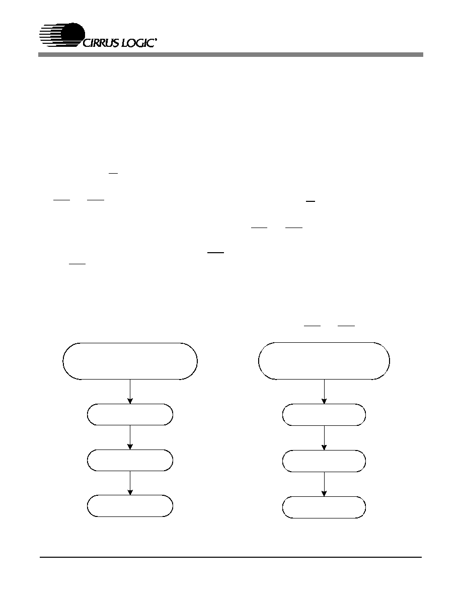
54
address of the desired Parallel I/O Register. The
address must be maintained for the duration of
the read cycle.
Host Message: FA[1:0]==00b.
Host Control:
FA[1:0]==01b.
PCMDATA:
FA[1:0]==10b.
CMPDATA:
FA[1:0]==11b.
2) The host indicates that this is a write cycle by
driving the FR/W pin low.
3) The host initiates a write cycle by driving the
FCS and FDS pins low.
4) The host drives the data byte to the FDAT[7:0]
pins of DSPAB.
5) Once the setup time for the write has been met,
the host ends the write cycle by driving the FCS
and FDS pins high.
6.2.6.2 Reading a Byte in Motorola Mode
The flow diagram shown in
Figure 39, "Motorola
Mode, One-Byte Read Flow Diagram for DSPAB"
on page 54
illustrates the sequence of events that
define a one-byte read in Motorola mode. The
protocol presented in
Figure 39
will now be
described in detail.
1) The host must drive the FA1 and FA0 register
address pins of DSPAB with the address of the
desired Parallel I/O Register. Note that only the
Host Message register and the Host Control
register can be read. The address must be
maintained for the duration of the read cycle.
Host Message:
FA[1:0]==00b.
Host Control:
FA[1:0]==01b.
2) The host indicates that this is a read cycle by
driving the FR/W pin high.
3) The host initiates the read cycle by driving the
FCS and FDS pins low (bus must be tri-stated
by this time).
4) Once the data is valid (after waiting the
appropriate time specified in the timing
specifications), the host can read the value of
the selected register from the FDAT[7:0] pins
of DSPAB.
5) The host should now terminate the read cycle
by driving the FCS and FDS pins high.
FCS (HIGH)
FDS (HIGH)
WRITE BYTE TO
FDAT[7:0]
FCS (LOW)
FDS (LOW)
FR/W (LOW)
ADDRESS A PARALLEL I/O REGISTER
(FA[1:0] SET APPROPRIATELY)
Figure 38. Motorola Mode, One-Byte Write Flow Dia-
gram for DSPAB
FCS (HIGH)
FDS (HIGH)
READ BYTE FROM
FDAT[7:0]
FCS (LOW)
FDS (LOW)
FR/W (HIGH)
ADDRESS A PARALLEL I/O REGISTER
(FA[1:0] SET APPROPRIATELY)
Figure 39. Motorola Mode, One-Byte Read Flow Di-
agram for DSPAB
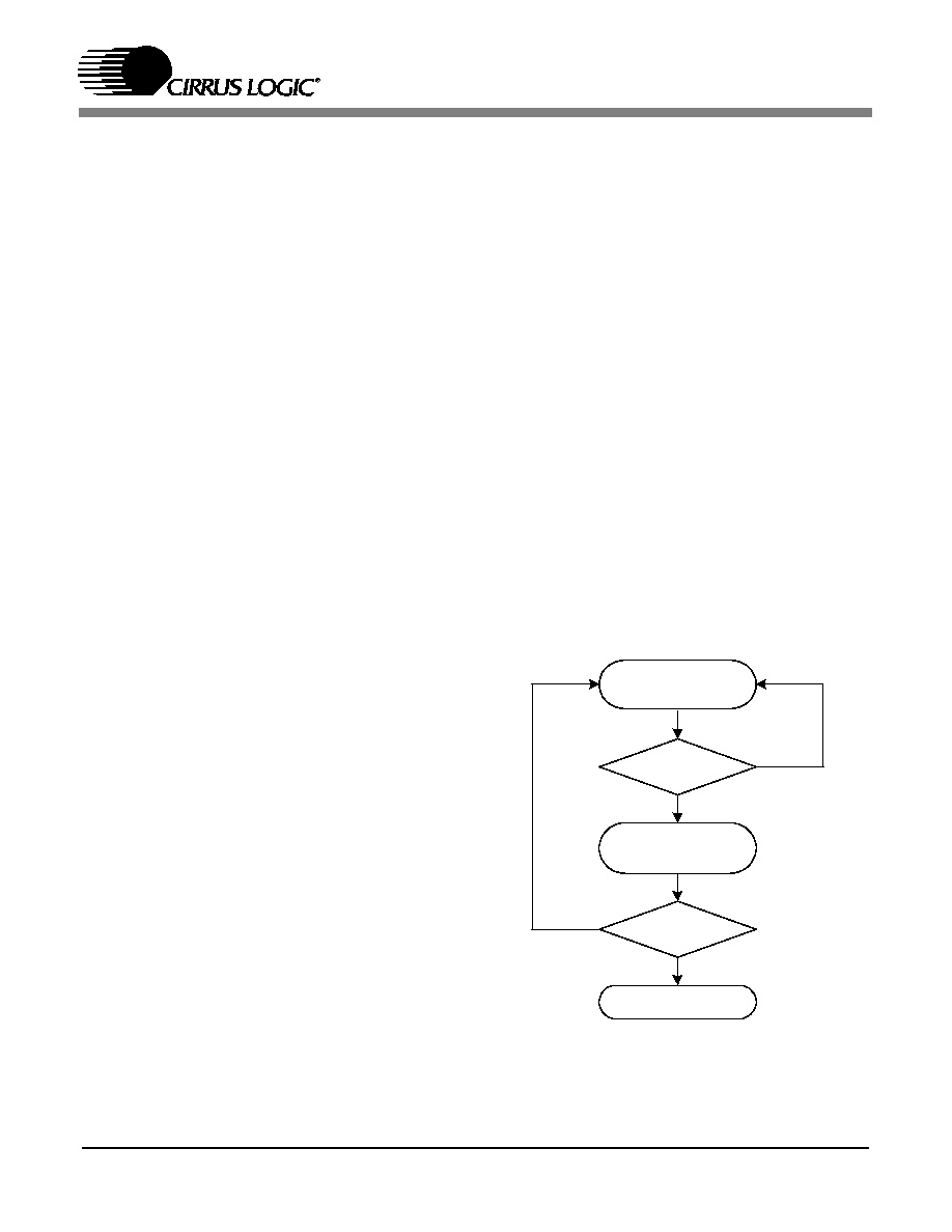
55
6.2.7 Procedures for Parallel Host Mode
Communication for DSPAB
6.2.7.1 Control Write in a Parallel Host Mode
for DSPAB
When writing control data to DSPAB, the same
protocol is used whether the host is writing a
control message or an entire executable download
image. Messages sent to DSPAB should be written
most significant byte first. Likewise, downloads of
the application code should also be performed most
significant byte first.
The example shown in this section can be
generalized to fit any control write situation. The
generic function `Read_Byte_*()' is used in the
following example as a generalized reference to
either Read_Byte_MOT() (read a byte in Motorola
mode) or Read_Byte_INT() (read a byte in Intel
mode), and `Write_Byte_*()' is a generic reference
to Write_Byte_MOT() (write a byte in Motorola
mode) or Write_Byte_INT() (write a byte in Intel
mode).
Figure 40
shows a typical write sequence.
The protocol presented in
Figure 40
will now be
described in detail.
1) When the host is communicating with DSPAB,
the host must verify that DSPAB is ready to
accept a new control byte. If DSPAB has not
read the previous byte from the control port, it
will be unable to receive another byte.
2) In order to determine whether DSPAB is ready
to accept a new control byte the host must read
the HINBSY bit of the Host Control Register
(bit 2 in FA[1:0]=01b) using the selected
communication mode (Intel or Motorola). If
HINBSY is high, then the DSP is not prepared
to accept a new control byte, and the host
should poll the Host Control Register again. If
HINBSY is low, then the host may write a
control byte into the Host Message Register.
3) Once the host knows that the DSP is ready for
a new control byte, it should write the control
byte to the Host Message Register (FA[1:0] =
00b) using the selected communication mode
(Intel or Motorola).
4) If the host would like to write any more control
bytes to DSPAB, the host should once again
poll the Host Control Register (return to step 1).
6.2.7.2 Control Read in a Parallel Host Mode
for DSPAB
When reading control data from DSPAB, the same
protocol is used whether the host is reading a single
byte, a 6 byte message, or a string of messages.
During the boot procedure, a handshaking protocol
is used by DSPAB. This handshake consists of a 3
byte write to DSPAB followed by a 1 byte response
from the DSP. The host must read the response byte
and act accordingly. The boot procedure is
discussed in
Section 8 "Boot Procedure" on page
71
.
During
regular operation (at run-time), the
responses from DSPAB will always be 6 bytes in
length.
MORE BYTES
TO WRITE?
READ_BYTE_*(HOST
CONTROL REGISTER)
N
FINISHED
Y
WRITE_BYTE_*(HOST
MESSAGE REGISTER)
HINBSY == 1
Y
N
Figure 40. Typical Parallel Host Mode Control
Write Sequence Flow Diagram for DSPAB
56
The example shown in this section can be used for
any control read situation. The generic function
`Read_Byte_*()' is used in the following example
as
a
generalized
reference
to
either
Read_Byte_MOT()
(Motorola
byte
read)
or
Read_Byte_INT() (Intel byte read).
Figure 41
shows a typical read sequence. The protocol
presented in
Figure 41
will now be described in
detail.
1) Optionally, FINTREQ going low may be used
as an interrupt to the host to indicate that
DSPAB has an outgoing message. Note that
even with the use of FINTREQ, HOUTRDY
must be checked to ensure that the current byte
is ready to be read by the host during the read
process. Please note that the state of FINTREQ
is undefined during boot, and it is valid only
once the application code is loaded.
2) The host reads the Host Control Register
(FA[1:0] = 01b) in order to determine the state
of the communication interface.
3) In order to determine whether DSPAB has an
outgoing control byte that is valid, the host
must check the HOUTRDY bit of the Host
Control Register (bit 1, FA[1:0] = 01b). If
HOUTRDY is high, then the Host Message
Register contains a valid message byte for the
host. If HOUTRDY is low, then the DSP has
not placed a new control byte in the Host
Message Register, and the host should poll the
Host Control Register again.
4) Once the host knows that the DSP is ready to
provide a new response byte, the host can
safely read a byte from the Host Message
Register (FA[1:0] = 00b) using the appropriate
communication protocol (Motorola or Intel).
5) If the host expects to read any more response
bytes, the host should once again check the
HOUTRDY bit (return to step 1). Messages
from the application code (post-download) on
the DSP will always be 6 bytes, unless
otherwise stated in the associated Application
Note.
6) After the response has been read the host
should wait at least 100 uS and check
HOUTRDY one final time. If HOUTRDY is
high once again this means that an unsolicited
message has come during the read process and
the host has another message to read (i.e. skip
back to step 4 and read out the new message). It
is the host's responsibility to insure that any
pending messages are read from the DSP.
F I N T R E Q = 0 ?
( o p t io n a l)
M O R E B Y T E S T O
R E A D ?
F I N IS H E D
R E A D _ B Y T E _ * ( H O S T
C O N T R O L R E G I S T E R )
Y
N
R E A D _ B Y T E _ * ( H O S T
M E S S A G E R E G I S T E R )
H O U T R D Y = = 1
Y
N
Y
R E A D _ B Y T E _ * ( H O S T
C O N T R O L R E G I S T E R )
H O U T R D Y = = 1
W A I T 1 0 0 M IC R O S E C
Y
N
Figure 41. Typical Parallel Host Mode Control Read
Sequence Flow Diagram for DSPAB

57
Failure to do this may cause the DSP's output
message buffer to overflow, corrupting any
pending outbound messages.
6.3 Parallel Host Communication for DSPC
The parallel host communication modes of DSPC
provide an 8-bit interface to the DSP. An Intel-style
parallel mode and a Motorola-style parallel mode
are supported. The host interface is implemented
using four communication registers within DSPC
as shown in
Table 8, "Parallel Input/Output
Registers for DSPC," on page 58
. The HOSTMSG
register is a 32 bit register.
Since there are only
eight data pins, only one byte can be transferred at
a time, but a full 32 bits are transferred in each read
or write to this register.
When the host is downloading code or configuring
the application code in DSPC, control messages
must be written to (and read from) the Host
Message register 32 bits at a time. The HINBSY
pin and the HINBSY bit in the Host Control
register are used during messaging sessions to
determine when DSPC can accept another 32-bit
word of control data. The HINBSY pin and the
HINBSY bit (in the Host Control register) go high
when the host writes 32 bits (4 bytes) to the
HOSTMSG register. The HINBSY pin and
HINBSY bit go low when DSPC reads the 32 bit
data from the register. The INTREQ pin goes low
and the HOUTRDY bit (in the Host Control
register) goes high when DSPC has an message that
must be read by the host.
The HOSTDATA1 and HOSTDATA2 registers
are used strictly for the transfer of audio data to
DSPC. The host cannot read from these two
registers. Support of these registers is DSPC
application code specific, see the appropriate
Application Note for availability.
A detailed description for each parallel host mode
will now be given. The following information will
be provided for the Intel mode and Motorola mode:
∑
The pins of DSPC which must be used for prop-
er communication
∑
Flow diagram and description for a parallel
byte write
∑
Flow diagram and description for a 32-bit word
(4-byte) write
∑
Flow diagram and description for a parallel
byte read
∑
Flow diagram and description for a 32-bit word
(4-byte) read
The four registers of DSPC's parallel host mode are
not used identically. The algorithm used for
communicating with each register will be given as
a functional description, building upon the basic
read and write protocols defined in the Motorola
and Intel sections. The following will be covered:
∑
Flow diagram and description for a control
write
∑
Flow diagram and description for a control read

58
6.3.1 Host Message (HOSTMSG) Register, A[1:0] = 00b
The HOSTMSG register is a 32-bit register that is
used to read from or write to DSPC. It is read and
written in 4-byte transactions. This register passes
all the code, control and configuration data to and
from DSPC. Messages are read and written
MS_BYTE first.
MS_BYTE
This is the most significant byte (bits 31:24).
BYTE_B
This is BYTE_B (bits 23:16).
BYTE_A
This is BYTE_A (bits 15:8).
LS_BYTE
This is the least significant byte (bits 7:0).
6.3.2 Host Control (CONTROL) Register, A[1:0] = 01b
Reserved
Always write a 0.
BYTE_SEL
Always write a 11b to these bits.
HINBSY
This bit is the Host Input Ready signal. It is set when the host writes to the HOSTMSG register.
It is cleared when DSPC reads the HOSTMSG register. This bit is also pinned out on the
HINBSY pin. Read only by the host and DSPC.
HOUTRDY
This bit is set when DSPC writes data to the HOST_MSG register, and indicates that the DSP
has a pending message for the host. The HOUTRDY bit is cleared when the host reads the
HOSTMSG register. The bit is inverted and pinned out on the INTREQ pin. Read only by the
host and DSPC
6.3.3 Host Data1 Input (HOSTDATA1) Register, A[1:0] = 10b
HOSTDATA1_7≠0
The host writes data to DSPC at this address. (Write only)
6.3.4 Host Data2 Input (HOSTDATA2) Register, A[1:0] = 11b
HOSTDATA2_7≠0
The host writes data to DSPC at this address. (Write only)
31
30
29
28
27
26
25
24
MS_BYTE
23
22
21
20
19
18
17
16
BYTE_B
15
14
13
12
11
10
9
8
BYTE_A
7
6
5
4
3
2
1
0
LS_BYTE
7
6
5
4
3
2
1
0
Reserved
Reserved
Reserved
BYTE_SEL
HINBSY
HOUTRDY
Reserved
7
6
5
4
3
2
1
0
HOSTDATA1_
7
HOSTDATA1_
6
HOSTDATA1_
5
HOSTDATA1_
4
HOSTDATA1_
3
HOSTDATA1_
2
HOSTDATA1_
1
HOSTDATA1_
0
7
6
5
4
3
2
1
0
HOSTDATA2_
7
HOSTDATA2_
6
HOSTDATA2_
5
HOSTDATA2_
4
HOSTDATA2_
3
HOSTDATA2_
2
HOSTDATA2_
1
HOSTDATA2_
0
Table 8. Parallel Input/Output Registers for DSPC
59
6.3.5 Intel Parallel Host Communication
Mode for DSPC
The Intel parallel host communication mode is
implemented using the pins given in
Table 9
.
Parallel host communication is available only on
the 144-pin package version of the CS49400.
The INTREQ pin is asserted (driven low)
whenever the DSP has an outgoing message for the
host. This same information is reflected by the
HOUTRDY bit of the Host Control Register
(A[1:0] = 01b).
INTREQ is useful for informing the host of
unsolicited messages. An unsolicited message is
defined as a message generated by the DSP without
an associated host read request.
6.3.5.1 Writing a Byte in Intel Mode for DSPC
Information provided in this section is intended as
a functional description of how to write control
information to DSPC. The system designer must
ensure that all of the timing constraints of the Intel
Parallel Host Mode Write Cycle are met.
The flow diagram shown in
Figure 42
illustrates
the sequence of events that define a one-byte write
in Intel mode. One-byte writes should only be
perfomed to the Host Control and Host Data
registers. The protocol presented in
Figure 42
will
now be described in detail.
1) The host must first drive the A1 and A0 register
address pins of DSPC with the address of the
desired Parallel I/O Register. The address is
latched on the falling edge of CS.
Host Control:
A[1:0]==01b.
Host Data1:
A[1:0]==10b.
Host Data2:
A[1:0]==11b.
2) The host initiates a write cycle by driving the
CS and WR pins low.
3) The host drives the data byte to the HDAT[7:0]
pins of DSPC.
4) Once the setup time for the write has been met,
the host ends the write cycle by driving the WR
and CS pins high.
Mnemonic
Pin Name
144-Pin
Package,
Pin
Number
Chip Select
CS
129
Write Enable
WR
120
Output Enable
RD
121
Register Address Bit 1
A1
139
Register Address Bit 0
A0
130
Interrupt Request
INTREQ
3
Host Busy
HINBSY
141
DATA7
HDAT7
95
DATA6
HDAT6
96
DATA5
HDAT5
97
DATA4
HDAT4
103
DATA3
HDAT3
105
DATA2
HDAT2
112
DATA1
HDAT1
115
DATA0
HDAT0
116
Table 9. Intel Mode Communication Signals for DSPC
CS (HIGH)
W R (HIGH)
W RITE BYTE TO
HDAT[7:0]
CS (LOW )
W R (LOW )
ADDRESS A PARALLEL I/O REGISTER
(A[1:0] SET APPROPRIATELY)
Figure 42. Intel Mode, One-Byte Write Flow Diagram
for DSPC
60
6.3.5.2 Writing a 32-bit (4-byte) Word in Intel
Mode for DSPC
Information provided in this section is intended as
a functional description of how to write control
information to DSPC. The system designer must
ensure that all of the timing constraints of the Intel
Parallel Host Mode Write Cycle are met.
The flow diagram shown in
Figure 43
illustrates
the sequence of events that define a 4-byte write in
Intel mode. 32-bit (4-byte) writes should only be
used to write to the Host Message register. The
protocol presented in
Figure 43
will now be
described in detail.
1) The host must first drive the A1 and A0 register
address pins of DSPC with the address of the
desired Parallel I/O Register (both low for
A1=A0=0). The address must be maintained
for the duration of the write cycle, and is
latched on the falling edge of CS and WR.
Host Message:
A[1:0]==00b.
2) The host initiates a write cycle by driving the
CS and WR pins low.
3) The host drives the most significant data byte
(bits 31:24) to the HDAT[7:0] pins of DSPC.
4) Once the setup time for the write has been met,
the host drives WR high to strobe in the most
significant data byte.
5) The host drives WR low.
6) The host drives the next most significant data
byte, BYTE_B (bits 23:16), to the HDAT[7:0]
pins of DSPC.
7) Once the setup time for the write has been met,
the host drives WR high to strobe in the data
byte.
8) The host drives WR low.
9) The host drives the next most significant data
byte, BYTE_A (bits 15:8), to the HDAT[7:0]
pins of DSPC.
10) Once the setup time for the write has been met,
the host drives WR high to strobe in the data
byte.
11) The host drives WR low.
12) The host drives the least significant data byte
(bits 7:0) to the HDAT[7:0] pins of DSPC.
13) Once the setup time for the write has been met,
the host drives WR high to strobe in the data
byte.
14) The host drives CS high to end the write
transaction.
6.3.5.3 Reading a Byte in Intel Mode for DSPC
Information provided in this section is intended as
a functional description of how to read control
information from DSPC. The system designer must
ensure that all of the timing constraints of the Intel
Parallel Host Mode Read Cycle are met.
The flow diagram shown in
Figure 44
illustrates
the sequence of events that define a one-byte read
in Intel mode. One-byte reads should only be done
with the Host Control register. The protocol
presented in
Figure 44
will now be described in
detail.
CS (HIGH)
RD (HIGH)
READ BYTE FROM
HDAT[7:0]
CS (LOW)
RD (LOW)
ADDRESS A PARALLEL I/O REGISTER
(A[1:0] SET APPROPRIATELY)
Figure 44. Intel Mode, One-Byte Read Flow Diagram
for DSPC
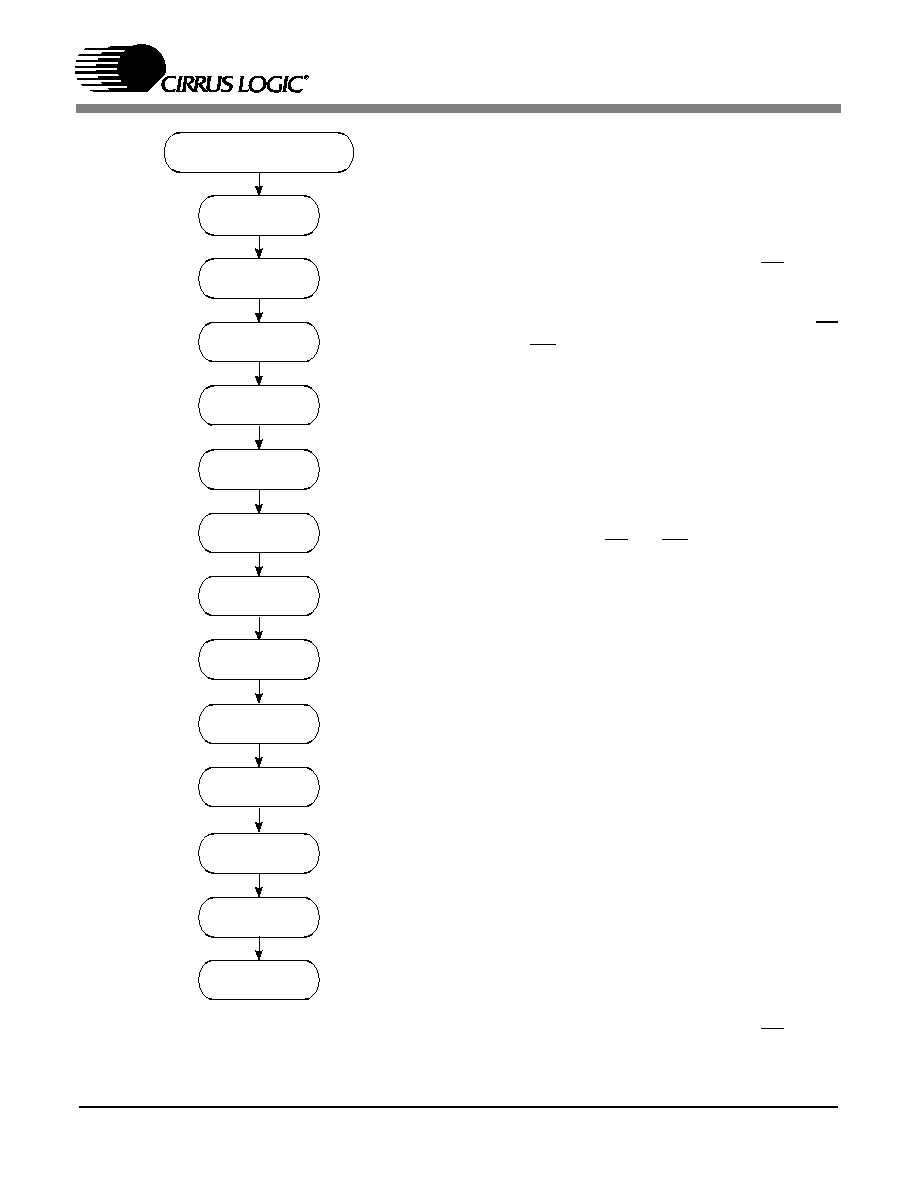
61
1) The host must first drive the A1 and A0 register
address pins of DSPC with the address of the
desired Parallel I/O Register (A1=0, A0=1).
Note that only the Host Control register can be
read using a byte read. The address must be
maintained for the duration of the read cycle,
and is latched on the falling edge of CS.
Host Control:
A[1:0]==01b.
2) The host initiates a read cycle by driving the CS
and RD pins low (bus must be tri-stated by this
time).
3) Once the data is valid (after waiting the
appropriate time specified in the timing
specifications), the host can read the value of
the selected register from the HDAT[7:0] pins
of DSPC.
4) The host should now terminate the read cycle
by driving the CS and RD pins high.
6.3.5.4 Reading a 32-bit (4-byte) Word from
DSPC in Intel Mode
Information provided in this section is intended as
a functional description of how to read control
information from DSPC. The system designer must
ensure that all of the timing constraints of the Intel
Parallel Host Mode Read Cycle are met.
The flow diagram shown in
Figure 45, "Intel
Mode, 32-Bit (4-Byte) Read Flow Diagram for
DSPC" on page 62
illustrates the sequence of
events that define a 4-byte read in Intel mode. 4-
byte (32-bit) reads should only be done with the
Host Message register. The protocol presented in
Figure 45
will now be described in detail.
1) The host must first drive the A1 and A0 register
address pins of DSPC with the address of the
desired Parallel I/O Register (A1=A0=0). Note
that only the Host Message register can be read
using a 4-byte read cycle. The address must be
maintained for the duration of the read cycle,
and is latched on the falling edge of CS.
Host Message:
A[1:0]==00b.
ADDRESSAPARALLELI/OREGISTER
(A[1:0] SETAPPROPRIATELY)
CS(HIGH)
CS(LOW)
WR(LOW)
WRITEMS_BYTETO
HDAT[7:0]
WR(HIGH)
WR(LOW)
WRITEBYTE_BTO
HDAT[7:0]
WR(HIGH)
WR(LOW)
WRITEBYTE_ATO
HDAT[7:0]
WR(HIGH)
WR(LOW)
WRITELS_BYTETO
HDAT[7:0]
WR(HIGH)
Figure 43. Intel Mode, 32-bit (4-byte) Write Flow
Diagram for DSPC

62
2) The host initiates a read cycle by driving the CS
and RD pins low (bus must be tri-stated by this
time).
3) Once the data is valid (after waiting the
appropriate time specified in the timing
specifications), the host can read the most
significant data byte (bits 31:24) from the
HDAT[7:0] pins of DSPC.
4) The host drives RD high to indicate that the
data byte has been read.
5) The host drives RD low to clock out the next
data byte.
6) Once the data is valid (after waiting the
appropriate time specified in the timing
specifications), the host can read BYTE_B (bits
23:16) from the HDAT[7:0] pins of DSPC.
7) The host drives RD high to indicate that the
data byte has been read.
8) The host drives RD low to clock out the next
data byte.
9) Once the data is valid (after waiting the
appropriate time specified in the timing
specifications), the host can read BYTE_A
(bits 15:8) from the HDAT[7:0] pins of DSPC.
10) The host drives RD high to indicate that the
data byte has been read.
11) The host drives RD low to clock out the next
data byte.
12) Once the data is valid (after waiting the
appropriate time specified in the timing
specifications), the host can read the least
significant data byte (bits 7:0) from the
HDAT[7:0] pins of DSPC.
13) The host drives RD high to indicate that the
data byte has been read.
14) The host should now terminate the read cycle
by driving the CS pin high.
ADDRESS A PARALLEL I/O REGISTER
(A[1:0] SET APPROPRIATELY)
CS (HIGH)
CS (LOW)
RD (LOW)
READ MS_BYTE FROM
HDAT[7:0]
RD (HIGH)
RD (LOW)
READ BYTE_B FROM
HDAT[7:0]
RD (HIGH)
RD (LOW)
READ BYTE_A FROM
HDAT[7:0]
RD (HIGH)
READ LS_BYTE FROM
HDAT[7:0]
RD (HIGH)
RD (LOW)
Figure 45. Intel Mode, 32-Bit (4-Byte) Read Flow
Diagram for DSPC

63
6.3.6 Motorola Parallel Host
Communication Mode for DSPC
The Motorola parallel host communication mode is
implemented using the pins given in Table 10.
Parallel host communication is available only on
the 144-pin package part. The INTREQ pin is
asserted (driven low) whenever the DSP has an
outgoing message for the host. This same
information is reflected by the HOUTRDY bit of
the Host Control Register (A[1:0] = 01b).
INTREQ is useful for informing the host of
unsolicited messages. An unsolicited message is
defined as a message generated by DSPC without
an associated host read request.
6.3.6.1 Writing a Byte in Motorola Mode for
DSPC
Information provided in this section is intended as
a functional description of how to write control
information to DSPC. The system designer must
ensure that all of the timing constraints of the
Motorola Parallel Host Mode Write Cycle are met.
The flow diagram shown in
Figure 46
illustrates
the sequence of events that define a one-byte write
in Motorola mode. One byte writes should only be
used with the Host Control and Host Data registers.
The protocol presented in
Figure 46
will now be
described in detail.
1) The host must first drive the A1 and A0 register
address pins of DSPC with the address of the
desired Parallel I/O Register. The address is
latched on the falling edge of CS.
Host Control:
A[1:0]==01b.
Host Data1:
A[1:0]==10b.
Host Data2:
A[1:0]==11b.
2) The host indicates that this is a write cycle by
driving the R/W pin low.
Mnemonic
Pin Name
144-Pin
Package,
Pin
Number
Chip Select
CS
129
Data Strobe
DS
120
Read or Write Select
R/W
121
Register Address Bit 1
A1
139
Register Address Bit 0
A0
130
Interrupt Request
INTREQ
3
Host Busy
HINBSY
141
DATA7
HDAT7
95
DATA6
HDAT6
96
DATA5
HDAT5
96
DATA4
HDAT4
103
DATA3
HDAT3
105
DATA2
HDAT2
112
DATA1
HDAT1
115
DATA0
HDAT0
116
Table 10. Motorola Mode Communication Signals for
DSPC
CS (HIGH)
DS (HIGH)
W RITE BYTE TO
HDAT[7:0]
CS (LOW )
DS (LOW )
R/W (LOW )
ADDRESS A PARALLEL I/O REGISTER
(A[1:0] SET APPROPRIATELY)
Figure 46. Motorola Mode, One-Byte Write Flow
Diagram for DSPC

64
3) The host initiates a write cycle by driving the
CS and DS pins low.
4) The host drives the data byte to the HDAT[7:0]
pins of DSPC.
5) Once the setup time for the write has been met,
the host ends the write cycle by driving the DS
and CS pins high.
6.3.6.2
Writing a 32-bit (4-byte) Word in
Motorola Mode for DSPC
Information provided in this section is intended as
a functional description of how to write control
information to DSPC. The system designer must
ensure that all of the timing constraints of the
Motorola Parallel Host Mode Write Cycle are met.
The flow diagram shown in
Figure 43
illustrates
the sequence of events that define a 32-bit (4-byte)
write in Motorola mode. 32-bit (4-byte) writes
should only be done to the Host Message register.
The protocol presented in
Figure 43
will now be
described in detail.
1) The host must first drive the A1 and A0 register
address pins of DSPC with the address of the
desired parallel I/O register (A1=A0=0). The
address must be maintained for the duration of
the write cycle, and is latched on the falling
edge of CS.
Host Message:
A[1:0]==00b.
2) The host indicates that this is a write cycle by
driving the R/W pin low.
3) The host initiates a write cycle by driving the
CS and DS pins low.
4) The host drives the most significant data byte
(bits 31:24) to the HDAT[7:0] pins of DSPC.
5) Once the setup time for the data has been met,
the host latches this byte in by driving DS high.
6) The host drive DS low.
7) The host drives the next most significant data
byte, BYTE_B (bits 23:16), to the HDAT[7:0]
R/W (LOW)
ADDRESS A PARALLEL I/O REGISTER
(A[1:0] SET APPROPRIATELY)
CS (HIGH)
CS (LOW)
DS (LOW)
WRITE MS_BYTE TO
HDAT[7:0]
DS (HIGH)
DS (LOW)
WRITE BYTE_B TO
HDAT[7:0]
DS (HIGH)
DS (LOW)
WRITE BYTE_A TO
HDAT[7:0]
DS (HIGH)
DS (LOW)
WRITE LS_BYTE TO
HDAT[7:0]
DS (HIGH)
Figure 47. Motorola Mode, 32-bit (4-byte) Write Flow
Diagram for DSPC

65
pins of DSPC.
8) Once the setup time for the data has been met,
the host latches this byte in by driving DS high.
9) The host drive DS low.
10) The host drives the next most significant data
byte, BYTE_A (bits 15:8), to the HDAT[7:0]
pins of DSPC.
11) Once the setup time for the data has been met,
the host latches this byte in by driving DS high.
12) The host drive DS low.
13) The host drives the least significant data byte
(bits 7:0) to the HDAT[7:0] pins of DSPC.
14) Once the setup time for the data has been met,
the host latches this byte in by driving DS high.
15) The host ends the write cycle by driving the CS
pin high.
6.3.6.3 Reading a Byte in Motorola Mode for
DSPC
Information provided in this section is intended as
a functional description of how to write control
information to DSPC. The system designer must
ensure that all of the timing constraints of the
Motorola Parallel Host Mode Read Cycle are met.
The flow diagram shown in
Figure 48
illustrates
the sequence of events that define a one-byte read
in Motorola mode. Single byte reads should only be
done with the Host Control register. The protocol
presented in
Figure 48
will now be described in
detail.
1) The host must first drive the A1 and A0 register
address pins of DSPC with the address of the
desired Parallel I/O Register (A1=0, A0=1).
The address must be maintained for the
duration of the read cycle, and is latched on the
falling edge of CS.
Host Control:
A[1:0]==01b.
2) The host indicates that this is a read cycle by
driving the R/W pin high.
3) The host initiates a read cycle by driving the CS
and DS pins low (bus must be tri-stated by this
time).
4) Once the data is valid (after waiting the
appropriate time specified in the timing
specifications), the host can read the value of
the selected register from the HDAT[7:0] pins
of DSPC.
5) The host should now terminate the read cycle
by driving the CS and DS pins high.
6.3.6.4 Reading a 32-bit (4-byte) word from
DSPC in Motorola mode
Information provided in this section is intended as
a functional description of how to read control
information from DSPC. The system designer must
ensure that all of the timing constraints of the
Motorola Parallel Host Mode Read Cycle are met.
The flow diagram shown in
Figure 49, "Motorola
Mode, 32-Bit (4-Byte) Read Flow Diagram for
DSPC" on page 66
illustrates the sequence of
events that define a 32-bit (4-byte) read in
Motorola mode. Reading a 32-bit (4-byte) word
should only be done with the Host Message
CS (HIGH)
DS (HIGH)
RE AD B YT E F ROM
HDA T[7 :0]
CS (LOW )
DS (LOW )
R/W (HIGH)
A DDRE SS A PA RALLE L I/O REGISTE R
(A [1:0 ] S ET AP PRO PRIA TE LY)
Figure 48. Motorola Mode, One-Byte Read Flow
Diagram for DSPC

66
register. The protocol presented in
Figure 49
will
now be described in detail.
1) The host must first drive the A1 and A0 register
address pins of DSPC with the address of the
desired Parallel I/O Register (A1=A0=0). Note
that only the Host Message register can be read
using 4-byte reads. The address must be
maintained for the duration of the read cycle,
and is latched on the falling edge of CS.
Host Message:
A[1:0]==00b.
2) The host indicates that this is a read cycle by
driving the R/W pin high.
3) The host initiates a read cycle by driving the CS
and DS pins low (bus must be tri-stated by this
time).
4) Once the data is valid (after waiting the
appropriate time specified in the timing
specifications), the host can read the most
significant
byte
(bits
31:24)
from
the
HDAT[7:0] pins of DSPC.
5) The host indicates the byte has been read by
driving DS high.
6) The host latches out the next byte by driving
DS low.
7) Once the data is valid (after waiting the
appropriate time specified in the timing
specifications), the host can read the next most
significant byte, BYTE_B (bits 23:16), of the
selected register from the HDAT[7:0] pins of
DSPC.
8) The host indicates the byte has been read by
driving DS high.
9) The host latches out the next byte by driving
DS low.
10) Once the data is valid (after waiting the
appropriate time specified in the timing
specifications), the host can read the next most
significant byte, BYTE_A (bits 15:8), of the
selected register from the HDAT[7:0] pins of
R/W (HIGH)
ADDRESS A PARALLEL I/O REGISTER
(A[1:0] SET APPROPRIATELY)
CS (HIGH)
CS (LOW)
DS (LOW)
READ MS_BYTE TO
HDAT[7:0]
DS (HIGH)
DS (LOW)
READ BYTE_B TO
HDAT[7:0]
DS (HIGH)
DS (LOW)
READ BYTE_A TO
HDAT[7:0]
DS (HIGH)
READ LS_BYTE TO
HDAT[7:0]
DS (HIGH)
DS (LOW)
Figure 49. Motorola Mode, 32-Bit (4-Byte) Read Flow
Diagram for DSPC

67
DSPC.
11) The host indicates the byte has been read by
driving DS high.
12) The host latches out the next byte by driving
DS low.
13) Once the data is valid (after waiting the
appropriate time specified in the timing
specifications), the host can read the least
significant byte (bits 7:0) of the selected
register from the HDAT[7:0] pins of DSPC.
14) The host indicates the byte has been read by
driving DS high.
15) The host should now terminate the read cycle
by driving the CS pin high.
6.3.7 Procedures for Parallel Host Mode
Communication for DSPC
6.3.7.1 Control Write in a Parallel Host Mode
for DSPC
When writing control data to DSPC, the same
protocol is used whether the host is writing a
control message or an entire executable download
image. Messages sent to DSPC should be written
most significant byte first. Likewise, downloads of
the application code should also be performed most
significant byte first.
The example shown in this section can be
generalized to fit any control write situation. The
generic function `Read_Byte_*()' is used in the
following example as a generalized reference to
either Read_Byte_MOT() (read a byte in Motorola
mode) or Read_Byte_INT() (read a byte in Intel
mode), and `Write_Byte_*()' is a generic reference
to Write_Byte_MOT() (write a byte in Motorola
mode) or Write_Byte_INT() (write a byte in Intel
mode).
Similarly,
the
generic
function
`Read_Word_*()' is used in the following example
as
a
generalized
reference
to
either
Read_Word_MOT() (read a 32-bit word in
Motorola mode) or Read_Word_INT() (read a 32-
bit word in Intel mode), and `Write_Word_*()' is a
generic reference to Write_Word_MOT() (write a
32-bit
word
in
Motorola
mode)
or
Write_Word_INT() (write a 32-bit word in Intel
mode).
Figure 50
shows a typical write sequence.
The protocol presented in
Figure 50
will now be
described in detail.
1) When the host is communicating with DSPC,
the host must verify that DSPC is ready to
accept a new 32-bit control word. If DSPC has
not read the previous word from the control
port, it will be unable to receive another word.
2) In order to determine whether DSPC is ready to
accept a new 32-bit control word the host must
read the HINBSY bit of the Host Control
Register (bit 2 in FA[1:0]=01b) using the
selected
communication
mode
(Intel
or
Motorola). If HINBSY is high, then the DSP is
not prepared to accept a new control word, and
the host should poll the Host Control Register
again. If HINBSY is low, then the host may
write a control word (32-bits) into the Host
MORE BYTES
TO WRITE?
READ_BYTE_*(HOST
CONTROL REGISTER)
N
FINISHED
Y
WRITE_WORD_*(HOST
MESSAGE REGISTER)
HINBSY == 1
Y
N
Figure 50. Typical Parallel Host Mode Control
Write Sequence Flow Diagram for DSPC
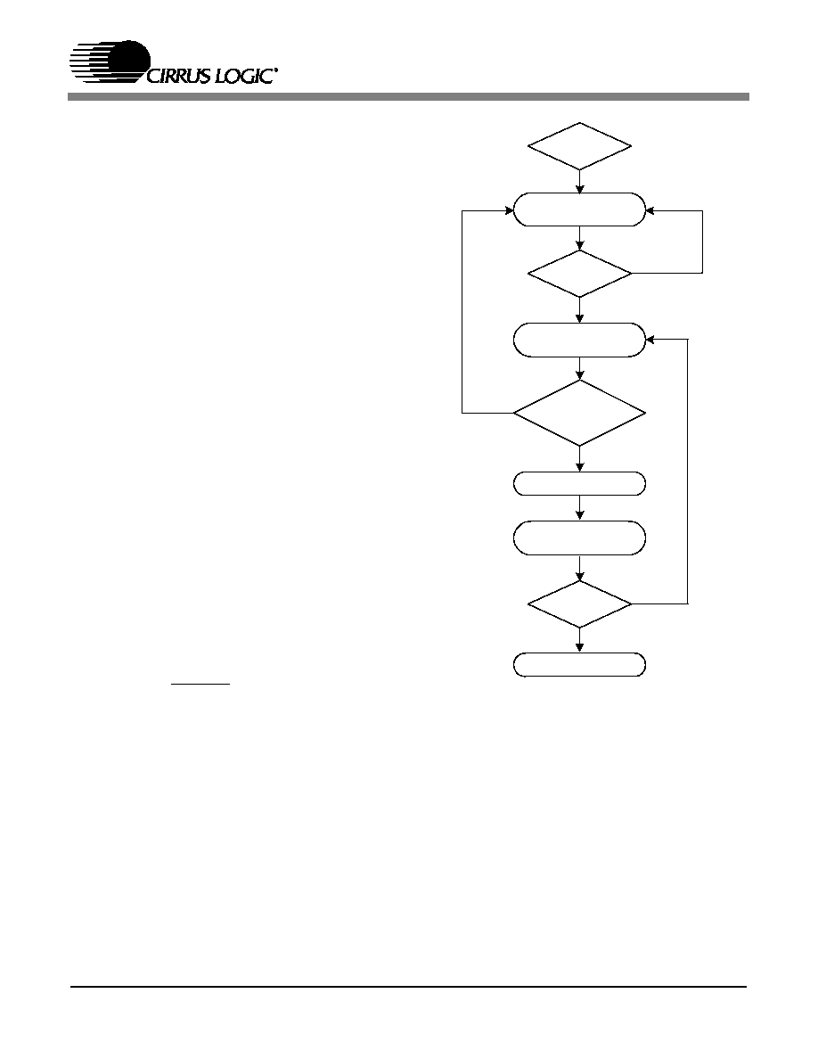
68
Message Register.
3) Once the host knows that the DSP is ready for
a new control word, it should write the 32-bit
control word to the Host Message Register
(FA[1:0]
=
00b)
using
the
selected
communication mode (Intel or Motorola).
4) If the host would like to write any more 32-bit
control words to DSPC, the host should once
again poll the Host Control Register (return to
step 1).
6.3.7.2 Control Read in a Parallel Host Mode
for DSPC
When reading control data from DSPC, the same
protocol is used whether the host is reading a single
32-bit word, or a string of message words.
Reads and writes to the Host Message Register are
always 32-bits (4-bytes), and reads of the Host
Control Register are always a single byte.
The example shown in this section can be used for
any control read situation. The generic function
`Read_Word_*()' is used in the following example
as
a
generalized
reference
to
either
Read_Word_MOT() (Motorola 32-bit word read)
or Read_Word_INT() (Intel 32-bit word read).
Figure 51
shows a typical read sequence. The
protocol presented in
Figure 51
will now be
described in detail.
1) Optionally, INTREQ going low may be used as
an interrupt to the host to indicate that DSPC
has an outgoing message.
2) The host reads the Host Control Register
(A[1:0] = 01b) in order to determine the state of
the communication interface.
3) In order to determine whether DSPC has an
outgoing control word that is valid, the host
must check the HOUTRDY bit of the Host
Control Register (bit 1, A[1:0] = 01b). If
HOUTRDY is high, then the Host Message
Register contains a valid 32-bit word for the
host. If HOUTRDY is low, then the DSP has
not placed a new control word in the Host
Message Register, and the host should poll the
Host Control Register again.
4) Once the host knows that the DSP is ready to
provide a new 32-bit response word, the host
can safely read a word from the Host Message
Register (A[1:0] = 00b) using the appropriate
communication protocol (Motorola or Intel).
5) If the host expects to read more 32-bit response
words, the host should once again check the
FINTREQ = 0?
MORE WORDS TO
READ?
FINISHED
READ_BYTE_*( HOST
CONTROL REGISTER)
Y
N
READ_WORD_*( HOST
MESSAGE REGISTER)
HOUTRDY == 1
Y
N
Y
READ_BYTE_*( HOST
CONTROL REGISTER)
HOUTRDY == 1
WAIT 100 MICROSEC
Y
N
Figure 51. Typical Parallel Host Mode Control Read
Sequence Flow Diagram for DSPC
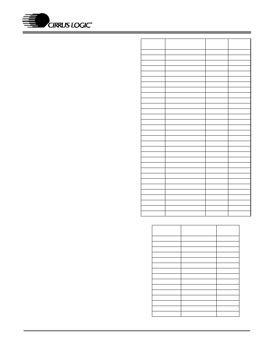
69
HOUTRDY bit (return to step 1).
6) After the response has been read the host
should wait at least 100 uS and check
HOUTRDY one final time. If HOUTRDY is
high once again this means that an unsolicited
message has come during the read process and
the host has another message to read (i.e. skip
back to step 4 and read out the new message). It
is the host's responsibility to insure that any
pending messages are read from the DSP.
Failure to do this may cause the DSP's output
message buffer to overflow, corrupting any
pending outbound messages.
7. EXTERNAL MEMORY
The system designer has the option of using
external memory. The external memory interface is
implemented with two controllers. The SRAM
controller allows the DSP to autoboot from a
parallel FLASH or EEPROM device. The SRAM
and SDRAM controllers are used to extend the data
memory of the DSP during runtime. A system can
use a FLASH/EEPROM device for autoboot, and
either SRAM or SDRAM for runtime memory. The
application user's guide for a particular code load
will inform the system designer if memory is
required, and will specify the memory type and
speed. If no mention is made of external memory,
then external memory is not required for that
application. The SDRAM interface is not
available on the 100-pin device.
The signals for the external memory interface
are listed in
Table 11
. and
Table 12
.
For both controllers, memory access speed is
controlled by the DSP clock setting which is
constrained by the application code. The SRAM
interface is capable of in-system programming a
FLASH device. Wait states are available to support
slower FLASH/EEPROM and SRAM devices. The
SRAM interface supports 1Mx8 addressable space.
We recommend 12nS or better SRAM for optimal
performance. The SDRAM interface supports
16Mbit parts organized as 512k x 16bits x 2 banks
which yields a 1Mx16 addressable space. The burst
Pin Name
Pin Description
144-Pin
Number
100-Pin
Number
EXTA0
SRAM Address 0
73
51
EXTA1
SRAM Address 1
74
52
EXTA2
SRAM Address 2
75
53
EXTA3
SRAM Address 3
76
54
EXTA4
SRAM Address 4
67
46
EXTA5
SRAM Address 5
66
45
EXTA6
SRAM Address 6
65
44
EXTA7
SRAM Address 7
63
43
EXTA8
SRAM Address 8
62
42
EXTA9
SRAM Address 9
60
41
EXTA10
SRAM Address 10
72
50
EXTA11
SRAM Address 11
56
40
EXTA12
SRAM Address 12
55
39
EXTA13
SRAM Address 13
54
38
EXTA14
SRAM Address 14
53
37
EXTA15
SRAM Address 15
52
36
EXTA16
SRAM Address 16
49
35
EXTA17
SRAM Address 17
47
34
EXTA18
SRAM Address 18
46
33
EXTA19
SRAM Address 19
71
N/A
EXTD0
SRAM Data 0
34
23
EXTD1
SRAM Data 1
35
24
EXTD2
SRAM Data 2
36
25
EXTD3
SRAM Data 3
37
26
EXTD4
SRAM Data 4
38
27
EXTD5
SRAM Data 5
40
28
EXTD6
SRAM Data 6
43
31
EXTD7
SRAM Data 7
44
32
NV_OE#
SRAM Output Enable
31
21
NV_WE#
SRAM Write Enable
71
N/A
NV_CS#
SRAM Chip Select
32
22
Table 11. SRAM Interface Pins
Pin Name
Pin Description
144-Pin
Number
SD_DATA0
SDRAM Data 0
34
SD_DATA1
SDRAM Data 1
35
SD_DATA2
SDRAM Data 2
36
SD_DATA3
SDRAM Data 3
37
SD_DATA4
SDRAM Data 4
38
SD_DATA5
SDRAM Data 5
40
SD_DATA6
SDRAM Data 6
43
SD_DATA7
SDRAM Data 7
44
SD_DATA8
SDRAM Data 8
56
SD_DATA9
SDRAM Data 9
55
SD_DATA10
SDRAM Data 10
54
SD_DATA11
SDRAM Data 11
53
SD_DATA12
SDRAM Data 12
52
SD_DATA13
SDRAM Data 13
49
SD_DATA14
SDRAM Data 14
47
Table 12. SDRAM Interface Pins
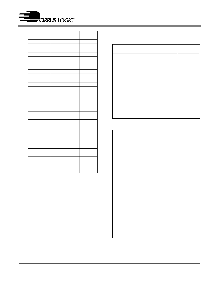
70
length is fixed to 8. We recommed SDRAM with a
CAS latency of 2 for optimal performance. The
refresh rate and the mode register of the SDRAM
must be set before Kickstart. Refer to Table 14,
"SDRAM Config Register," on page 70 for details
on the SDRAM config register. The SDRAM is
initialized after Kickstart.
7.1 Configuring SRAM Timing Parameters
Since not all SRAM manufacturers conform to the
exact same timing specifications, it is necessary to
configure
the
DSP
to
match
the
timing
specifications of the particular SRAM that is used
in your design. This message must be sent before
Kickstarting the downloaded DSPC application
code.
SD_DATA15
SDRAM Data 15
46
SD_ADDR0
SDRAM Address 0
73
SD_ADDR1
SDRAM Address 1
74
SD_ADDR2
SDRAM Address 2
75
SD_ADDR3
SDRAM Address 3
76
SD_ADDR4
SDRAM Address 4
67
SD_ADDR5
SDRAM Address 5
66
SD_ADDR6
SDRAM Address 6
65
SD_ADDR7
SDRAM Address 7
63
SD_ADDR8
SDRAM Address 8
62
SD_ADDR9
SDRAM Address 9
60
SD_ADDR10
SDRAM Address
10
72
SD_DQM0
SDRAM Data
Mask Output0
39
SD_WE#
SDRAM Write
Enable
37
SD_CAS#
SDRAM Column
Address Strobe
78
SD_RAS#
SDRAM Row
Address Strobe
77
SD_CS#
SDRAM Chip
Select
68
SD_BA
SDRAM Bank
Select
71
SD_DQM1
SDRAM Data
45
SD_CLK_IN
SDRAM Clock
Input
61
SD_CLK_OUT
SDRAM Clock
Output
59
SD_CLK_EN
SDRAM Clock
Enable
64
Pin Name
Pin Description
144-Pin
Number
Table 12. SDRAM Interface Pins
Mnemonic
Hex
Message
SRAM_CONTROLLER_TIMING
0xaaa = 0www wwrr rrre (in binary)
w = SRAM_FLASH_WR_CYCLE vari-
able found in the SRAM Switching char-
acteristics table in Section 1.19.
r = SRAM_FLASH_RD_CYCLE variable
found in the SRAM Switching character-
istics table in Section 1.19.
e = SRAM Enable/Disable = 0/1.
Default, aaa = 0x000
0x8100000F
0x00000aaa
Table 13. SRAM Controller Timing
Mnemonic
Hex
Message
SDRAM_CONFIG
aaaa = Auto refresh setting.
For example for a 16
µS refresh period
and a DCLK of 86 Mhz the value pro-
grammed should be:
16X10
-6
X 86X10
6
= 0x(1376) = 0x0560
bbb = Mode register setting. These bits
set the 12 least significant bits in the
mode register. The bits are to the follow-
ing by default:
bits(2..0) = 011 = Burst length 8.
bit3 = 0 = Sequential Burst Type.
bits(6..4) = 010 = CAS latency of 2.
bits(8..7) = 00 = Mode Register Set.
bit9 = 0 = Write Burst.
bit(12..10) = 000 = reserved
e = SDRAM Enable/Disable
=0001/0000.
Default, 0xaaaabbbe = 0x0560008c0
0x81000017
0xaaaabbbe
Table 14. SDRAM Config Register

71
8. BOOT PROCEDURE
In this section the process of booting and
downloading to the CS49400 will be covered as
well as how to perform a soft reset. There are two
ways to boot the DSP:
∑
Host Controlled MasterBoot
∑
Host Boot Via DSPC
Each of these boot procedures will be described in
detail with pseudocode. The flow charts use the
following messages:
∑
Write-C_* Write to DSPC
∑
Read-C_* Read from DSPC
∑
Write-AB_* Write to DSPAB
∑
Read-AB_* Read from DSPAB
Note:
When reading from DSPAB the host must
wait for FINTREQ to fall before starting the read
cycle. When reading from DSPC the host must
wait for INTREQ to fall before starting the read
cycle.
Note:
The * can be replaced by SPI, INTEL, or
MOT depending on the mode of host
communication. For each case the general
download algorithm is the same.
Table 16,
and
Table 17
define the boot write
messages and boot read messages in mnemonic and
actual hex value for DSPAB and DSPC. These
messages will be used in the boot sequence
8.1 Host Controlled Master Boot
A host controlled master boot is a sequence where
a host instructs the DSP to load application code
into itself from external memory. External memory
can either be FLASH or SPI EEPROM.
The
flow
chart given
in
Figure 52, "Host
Controlled Master Boot (Downloading both a
DSPAB
Application
Code
and
a
DSPC
Application Code)" on page 72
demonstrates the
interaction required by the microcontroller when
placing the DSP into a host controlled master
mode.
1) A download sequence is started when the host
holds the mode pins appropriately (UHS[2:0]
and FHS[1:0]) and toggles RESET.
2) The
host
must
then
send
the
C_MASTER_SOURCE_MODE boot message
MNEMONIC
VALUE
AB_APP_START
0x03
AB_APP_FAILURE
0xF0
Table 15. Application Messages from DSPAB
MNEMONIC
VALUE
C_RESERVED
0x00 00 00 00
C_SOFT_RESET
0x40 00 00 00
Table 16. Boot Write Messages for DSPC
C_SLAVE_MODE
0x80 00 00 00
C_MASTER_BOOT_FLASH
1110 wwww wrrr rrAA
AAAA AAAA AAAA AAAA
Where
w = SRAM_FLASH_WR_CYCLE
variable found in the SRAM Switch-
ing characteristics table in Section
1.19.
r = SRAM_FLASH_RD_CYCLE
variable found in the SRAM Switch-
ing characteristics table in Section
1.19.
A = 18-bit start address/4
0xEw cb AA AA
MNEMONIC
VALUE
C_BOOT_START
0x00 00 00 01
C_BOOT_SUCCESS
0x00 00 00 02
C_APP_START
0x00 00 00 04
C_BOOT_ERROR_CHECKSUM
0x00 00 00 FF
INVALID_BOOT_TYPE
0x00 00 00 FE
Table 17. Boot Read Messages from DSPC
Table 16. Boot Write Messages for DSPC (Continued)
b
c

72
STAR T
IN TR EQ LO W ?
MSG
==C _BO OT_START
IN TR EQ LO W ?
MSG ==
AB_ APP_START
AB_APPLICATIO N_R UN NIN G
R ESET(LO W )
RESET(H IG H)
W AIT ?? u S
W RITE-C_*
(C_M ASTER_SO U RC E_MO DE)
TIMEO UT
A FTER (10 m S)
TIM EO UT
AFTE R (500 m S)
RE AD-C_*(C_M ESSAG E)
R EAD-AB_*(A B_MESS AGE )
EX IT(ERR OR )
EXIT(E RRO R )
W R ITE -AB_*(AB_H W _C O NFIG_ MSG ,
MS G_ SIZE)
W RITE-AB_*(AB_SW _ CO NFIG _MSG ,
MS G_ SIZE)
W RITE-AB_*(KICKSTAR T,
MS G_ SIZE)
N
Y
N
Y
N
Y
N
Y
TIMEO UT
AFTER (10 mS )
N
Y
MSG ==
C_B OO T_SUC CES S
C _APPL ICATIO N_R UN NIN G
EXIT(ER RO R)
W R ITE-C_*(C_ HW _ CO NFIG _MSG ,
MS G_ SIZE)
W RITE-C _*(C_SW _CO N FIG _M SG,
MS G_ SIZE)
W RITE-C_*(KICKS TAR T,
MS G_ SIZE)
N
Y
R EAD-C_ *(C_ MESSAG E)
RELEAS E
C ON TR O L O F B US
W RITE-C_*(C_SO FT_ RESET)
INTREQ LO W ?
MSG ==
C_ APP_START
TIMEO U T
AFTER (10 mS)
READ -C _*(C _ME SSAG E)
EXIT(ER RO R)
N
N
Y
Y
IN TR EQ LO W ?
MSG
==C _BO OT_START
INTREQ LO W ?
W RITE-C_*
(C_M ASTER_SO U RC E_MO DE)
TIMEO UT
A FTER (10 m S)
TIM EO UT
AFTE R (500 m S)
RE AD-C_*(C_M ESSAG E)
EX IT(ERR OR )
N
Y
N
Y
N
Y
M SG ==
C _BO OT_SU CC ESS
EXIT(ER RO R)
N
Y
R EAD-C_*(C_ MESSAG E)
RELEAS E
C ON TR O L O F B US
FINTREQ LO W ?
HO UTRD Y HI?
Figure 52. Host Controlled Master Boot
(Downloading both a DSPAB Application Code and a DSPC Application Code)

73
to
DSPC.
The
supported
messages
are
described in Table 16. This message tells
DSPC where to get the DSPAB image from.
Currently the C_MASTER_BOOT_FLASH
message is supported and allows booting from
external byte-wide flash or eprom.
3) If the initialization was successful DSPC sends
out the C_BOOT_START message and the
host must proceed to step 4. If initialization
fails the host must re-try steps 1 through 3 and
if failure is met again, the communication
timing and protocol should be inspected.
4) After
receiving
the
C_BOOT_START
message, the host must release control of the
communication interface and wait for INTREQ
to go low.
Note:
DSPC will autoboot DSPAB. After this
DSPC will release control of the communication
interface, but only when in SPI Master Boot
Mode.
5) The end of the .ULD file contains a three byte
checksum. If the checksum is good after the
download,
DSPC
will
send
a
C_BOOT_SUCCESS message to the host. If
the checksum was bad, DSPC responds with
the C_BOOT_ERROR_CHECKSUM message
message and waits for a hard reset.
6) After reading out the C_BOOT_SUCCESS
message, the host must send a second
C_MASTER_SOURCE_MODE boot message
to DSPC. This messages tells DSPC where the
to get image for DSPC.
7) If the initialization was successful DSPC sends
out the C_BOOT_START message and the
host must proceed to step 8. If initialization
fails the host must re-try step 6. If failure is met
again, the communication timing and protocol
should be inspected.
8) After
receiving
the
C_BOOT_START
message, the host must release control of the
communication interface and wait for INTREQ
to go low.
Note:
DSPC will autoboot DSPC. After this
DSPC will release control of the communication
interface, but only when in SPI Master Boot
Mode.
9) The end of the .ULD file contains a four byte
checksum. If the checksum is good after the
download,
DSPC
will
send
a
C_BOOT_SUCCESS message to the host. If
the checksum was bad, DSPC responds with
the C_BOOT_ERROR_CHECKSUM message
and waits for a hard reset.
10) After reading out the C_BOOT_SUCCESS
message,
the
host
must
send
the
C_SOFT_RESET message which will cause
the application code to reset and allow the
downloaded application to run.
11) If the soft reset was successful, DSPC sends out
a C_APP_START message the host can
proceed to step 12. If DSPC does not send an
the application start message, the host must re-
try the whole procedure again.
12) Next the host can send hardware and software
configuration messages for DSPC.
13) At this point the application code on DSPC is
running and the host needs to configure
DSPAB.
14) The host must read the AB_APP_START
message from DSPAB. If DSPAB does not
send an the application start message the host
must re-try the whole procedure again, starting
with step 1.
15) The host must send hardware and software
configuration messages for DSPAB, ending
with the kickstart message.
16) At this point the application code on DSPAB is
running.
Note:
Hardware configuration messages are
used to define the behavior of the DSP's audio
ports. A more detailed description of the
different hardware configurations can be found

74
in the
Section 10 "Hardware Configuration" on
page 78
.
Note:
The software configuration messages
are specific to each application. The application
code user's guide for each application provides
a list of all pertinent configuration messages.
Writing the KICKSTART message to DSPAB
begins the audio decode process.
8.2 Host Boot Via DSPC
A host controlled boot via DSPC is a sequence
where the host boots DSPAB and DSPC through
DSPC with two separate images (.ULD files).
Figure 53, "Host Boot Via DSPC" on page 75
demonstrates the interaction required by the
microcontroller.
1) A download sequence is started when the host
holds the mode pins appropriately (UHS[2:0]
and FHS[1:0]) and toggles RESET.
2) The
host
must
then
send
the
C_SLAVE_MODE boot message to DSPC.
This causes DSPC to initialize itself.
3) If the initialization was successful DSPC sends
out a C_BOOT_START message. The host
should proceed to step 4. If initialization fails,
the host should re-try steps 1 through 3 and if
failure is met again, the communication timing
and protocol should be inspected.
4) After
receiving
the
C_BOOT_START
message,
the
host
should
write
the
downloadable image for DSPAB(.ULD file) to
DSPC.
5) The host must wait for INTREQ to go low and
read the message from DSPC.
6) After reading out the C_BOOT_SUCCESS
message,
the
host
must
then
send
the
C_SLAVE_MODE message to DSPC once
more. This causes DSPC to initialize itself and
get ready to accept a stream.
7) If the initialization was successful DSPC sends
out a C_BOOT_START message. The host
should proceed to step 8. If initialization fails,
the host should re-try step 6. If failure is met
again, the communication timing and protocol
should be inspected.
8) After
receiving
the
C_BOOT_START
message,
the
host
should
write
the
downloadable image for DSPC.
9) The host must wait for INTREQ to go low and
read the message from DSPC.
10) After reading out the C_BOOT_SUCCESS
message.
The
host
must
send
the
C_SOFT_RESET message which will cause
the application code to reset and allow the
downloaded application to run.
11) If the soft reset was successful, DSPC sends out
a C_APP_START message the host can
proceed to step 8. If DSPC does not send an the
application start message, the host must re-try
the whole procedure again.
12) Next the host can send hardware and software
configuration messages for DSPC.
13) At this point the application code on DSPC is
running and the host needs to configure
DSPAB.
14) The host must read the AB_APP_START
message from DSPAB. If DSPAB does not
send an the application start message the host
must re-try
the whole
procedure again,
beginning at setp 1.
15) The host must send hardware and software
configuration messages for DSPAB.
16) At this point the application code on DSPAB is
running.
Note:
Hardware configuration messages are
used to define the behavior of the DSP's audio
ports. A more detailed description of the
different hardware configurations can be found
in the
Section 10 "Hardware Configuration" on
page 78
.
Note:
The software configuration messages
are specific to each application. The application
code user's guide for each application provides

75
STAR T
INTR EQ LO W ?
MSG
==C_ BOOT_S TA RT
FINTR EQ LOW ?
HOU TR DY H I?
MSG==
AB _AP P_STA RT
AB_ AP PLIC ATION _R UN NIN G
RE SET(LO W )
R ESE T(HIGH)
W A IT 10 uS
W RITE -C _*
(C_SL AVE _MOD E)
TIME OUT
AFTER (5 m S)
TIME OUT
A FTER (5 m S )
RE AD-C_ *(C_ MES SAGE )
W R ITE-C_ *(.U LD FILE ,FILE
S IZE) for DS P AB
REA D -AB _*(A B_ME SSA GE)
EXIT(ER ROR )
EXIT(ER R OR)
W RITE -AB _*(AB_H W _C ON FIG_MSG,
M SG_SIZE )
W R ITE-A B_ *(AB _SW _ CON FIG_MS G,
M SG_SIZE )
W RITE-AB_*(KIC K START,
M SG_SIZE )
N
Y
N
Y
N
Y
N
Y
INTR EQ LO W ?
TIME OU T
A FTER (5 mS )
N
Y
MSG==
C_BOOT_S UC CE SS
C_ AP PLIC ATION _R UN NIN G
EXIT(E RR OR)
W RITE -C _*(C_H W _C ONFIG_ MSG,
MSG_S IZE)
W R ITE-C_ *(C_ SW _ CON FIG_MSG,
M SG_SIZE )
W R ITE-C_*(KIC KS TA RT,
M SG_SIZE )
N
Y
RE AD -C _*(C _M ESSA GE)
W R ITE-C_*(C_ SOFT_RE SET)
IN TR EQ L OW ?
MSG==
C_A PP_S TA R T
TIME OU T
A FTER (5 m S )
R EA D-C_*(C_ME SS AGE)
E XIT(ERR OR )
N
N
Y
Y
INTR EQ LO W ?
MSG
==C_ BOOT_S TA RT
W RITE -C _*
(C_SL AVE _MOD E)
TIME OUT
AFTER (5 m S)
RE AD-C_ *(C_ MES SAGE )
W R ITE-C_ *(.U LD FILE ,FILE
S IZE) for D SP C
EXIT(ER ROR )
N
Y
N
Y
INTR EQ LO W ?
TIME OU T
A FTER (5 mS )
N
Y
MSG==
C _B OOT_ SUC CE SS
EXIT(ER R OR )
N
RE AD -C _*(C _MES SA GE )
Figure 53. Host Boot Via DSPC

76
a list of all pertinent configuration messages.
Writing the KICKSTART message to DSPAB
begins the audio decode process.
9. SOFT RESETTING THE CS49400
Soft resetting the CS49400 uses a combination of
software and hardware. This method of resetting
the DSP is usually referred to as a "soft reset" even
though it involves toggling the reset pin due to the
fact that a soft reset message is sent to the DSP. To
soft reset the device, a previous application code
must have been downloaded without power cycling
the DSP.
Figure 54, "Host Controlled Master
Softreset" on page 77
describes the soft reset
procedure. The main purpose behind a soft reset is
to take advantage of the fact that all AC-3 based
codes can accept both AC-3 compressed data as
well as PCM data. This allows for a the host to
reconfigure the AC-3 application code for PCM or
AC-3 without having to completely redownload the
same application code.
9.1 Host Controlled Master Soft Reset
This reset procedure is used to restart the
application code that has already been loaded on
the DSP. All writes and reads with the CS49400
should follow the protocol given in
Section 8
"Boot Procedure" on page 71
.
1) A Soft Reset sequence is started when the host
holds the mode pins appropriately (UHS[2:0]
and FHS[1:0]) and toggles RESET.
2) The host must send the C_SOFT_RESET
message to DSPC. This causes the application
code on DSPAB and DSPC to reset and allow
the downloaded application to run.
3) If the soft reset was successful, DSPC sends out
a C_APP_START message the host can
proceed to step 4. If DSPC does not send an the
application start message, the host must re-try
the whole procedure again.
4) The host can send hardware and software
configuration messages for DSPC.
5) At this point the application code on DSPC is
running and the host needs to configure
DSPAB.
6) Next the host must wait for FINTREQ to go
low and read the AB_APP_START message
from DSPAB. If DSPAB does not send an the
application start message the host must re-try
the whole procedure again, beginning from step
1.
7) The host must send hardware and software
configuration messages for DSPAB.
8) At this point the application code on DSPAB is
running.
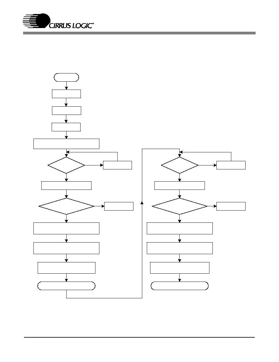
77
S TA RT
M SG==
A B_APP _S TART
AB _AP PLICATION _RUNNING
RES ET(LOW )
RES ET(HIGH)
W AIT 10 uS
RE A D-AB _*(AB _M E SS AGE)
E XIT(E RROR)
W RITE-AB _*(A B_HW _CONFIG_M S G,
MS G_SIZE)
W RITE-AB _*(A B_S W _CONFIG_MS G,
MS G_SIZE)
W RITE-A B_*(K IC KS TA RT,
MS G_SIZE)
N
Y
FINTREQ LOW ?
TIME OUT
A FTE R (5 m S )
N
Y
C _A PP LICA TION_RUNNING
W RITE -C_*(C_HW _CONFIG_M S G,
MSG_S IZE)
W RITE -C_*(C_S W _CONFIG_MS G,
MSG_S IZE)
W RITE -C_*(K ICK START,
MSG_S IZE)
W RITE-C_*(C_S OFT_RES ET)
INTRE Q LOW ?
MS G==
C_AP P_S TA RT
TIM EOUT
AFTE R (5 m S)
REA D-C_*(C_ME SS AGE)
E XIT(ERROR)
N
N
Y
Y
Figure 54. Host Controlled Master Softreset

78
10. HARDWARE CONFIGURATION
After download or soft reset, and before kickstart,
the host has the option of changing the default
hardware configuration. (Please see the Audio
Manager in the Application Messaging Section of
any Application Code User's Guide for more
information on kickstarting.)
Hardware configuration messages are used to
physically reconfigure the hardware of the audio
decoder, as in enabling or disabling address
checking for the serial communication port.
Hardware configuration messages are also used to
initialize the data type (i.e., PCM or compressed)
and format (e.g., I
2
S, left justified, etc.) for digital
data inputs, as well as the data format and clocking
options for the digital output port.
In general, the hardware configuration can only be
changed immediately after download or after soft
reset
and
before
kickstart.
However,
some
applications provide the capability to change the
input ports without affecting other hardware
configurations, after sending a special Application
Restart message. (Please see the Audio Manager in
any Application Code User's Guide to determine
whether the Application Restart message is
supported.)
11. DIGITAL INPUT AND OUTPUT
DATA FORMATS
The CS49400 supports a wide variety of data input
and output data formats through various input and
output ports. Hardware availability is entirely
dependent on whether the software application
code being used supports the required mode. This
data sheet presents most of the modes available
with the CS49400 hardware. This does not mean
that all of the modes are available with any
particular
piece
of
application
code.
The
Application Code User's Guide for the particular
code being used should be referenced to determine
if a particular mode is supported. In addition if a
particular mode is desired that is not presented,
please contact your local FAE as to its availability.
11.1 Digital Audio Formats
This subsection will describe some common audio
formats that the CS49400 supports. It should be
noted that the input ports use up to 24-bit PCM
resolution and 16-bit compressed data word
lengths. The output port of the CS49400 provides
up to 24-bit PCM resolution.
11.1.1 I
2
S
Figure 55, "I
2
S Format" on page 79
shows the I
2
S
format. For I
2
S, data is presented most significant
bit first, one FSCLKN1 delay after the transition of
FLRCLKN1, and is valid on the rising edge of
FSCLKN1. For the I
2
S format, the left subframe is
presented when FLRCLKN1 is low; the right
subframe is presented when FLRCLKN1 is high.
FSCLKN1 is required to run at a frequency of 48Fs
or greater on the input ports.
11.1.2 Left Justified
Figure 56, "Left Justified Format (Rising Edge
Valid SCLK)" on page 79
shows the left justified
format with a rising edge FSCCLK. Data is
presented most significant bit first on the first
FSCLKN1 after an FLRCLKN1 transition and is
valid on the rising edge of FSCLKN1. For the left
justified format, the left subframe is presented
when FLRCLKN1 is high and the right subframe is
presented when FLRCLKN1 is low. The left
justified format can also be programmed for data to
be valid on the falling edge of FSCLKN1.
FSCLKN1 is required to run at a frequency of 48Fs
or greater on the input ports.
11.2 Digital Audio Input Port
The digital audio input port (DAI) on DSPAB, is
used for both compressed and PCM digital audio
data input. In addition this port supports a special
clocking mode in which a clock can be input to
directly drive the internal 33 bit counter.
Table 18,
"Digital Audio Input Port," on page 79
shows the

79
pin names, mnemonics and pin numbers associated
with the DAI.
The DAI is fully configurable including support for
I
2
S and left-justified formats. DAI is programmed
for
slave
clocks,
where
FLRCLKN1
and
FSCLKN1 are inputs. All DAI configuration
messages must be sent to DSPAB.
11.3 Compressed Data Input Port
The compressed data input port (CDI) on DSPAB
can be used for both compressed and PCM data
input.
Table 19
shows the mnemonic, pin name,
and pin number of the pins associated with the CDI
port on the CS49400.
The CDI port is fully configurable for all data
formats
including:
I
2
S,
left-justified
and
multichannel formats. FLRCLKN2 and FSCLKN2
on the CDI port are programmed to be inputs. All
CDI configuration messages must be sent to
DSPAB.
11.4 Input Data Hardware Configuration
for CDI and DAI on DSPAB
Both data format (I
2
S, Left Justified) and data type
(compressed or PCM) are required to fully define
the input port's hardware configuration. The DAI
and the CDI are configured by the same group of
messages
since
their
configurations
are
interrelated. The naming convention of the input
hardware configuration is as follows:
INPUT A B C
where A, B, C and are the parameters used to fully
define the input port. The parameters are defined as
follows:
A - Data Type
B - Data Format
C - SCLK Polarity
Pin Name
Pin Description
144-Pin
Package,
Pin
Number
100-Pin
Package,
Pin
Number
FSDATAN1
Serial Data In
131
84
FSCLKN1
FSTCCLK2
Serial Bit Clock
Secondary STC
Clock
134
81
FLRCLKN1
Frame Clock
119
85
Table 18. Digital Audio Input Port
FLRCLKN1
FSCLKN1
FSDATAN1
MSB
LSB
Left
Right
MSB
LSB
Figure 55. I
2
S Format
FLRCLKN1
FSCLKN1
FSDATAN1
MSB
LSB
Left
Right
MSB
LSB
MSB
Figure 56. Left Justified Format (Rising Edge Valid SCLK)
Pin Name
Pin Description
144-Pin
Package,
Pin
Number
100-Pin
package,
Pin
Number
FSDATAN2
CMPDAT
Serial Data In
Compressed Data
In
118
79
FSCLKN2
CMPCLK
Serial Bit Clock
111
78
FLRCLKN2
CMPREQ
Frame Clock
Data Request Out
117
80
Table 19. Compressed Data Input Port

80
The following tables show the different values for
each parameter as well as the hex message that
needs to be sent. When creating the hardware
configuration message, only one hex message
should be sent per parameter. It should be noted
that the entire B parameter hex message must be
sent, even if one of the input ports has been defined
as unused by the A parameter.
11.4.1
Input Configuration Considerations
1) 24-bit PCM input requires at least 24 SCLKs
per sub-frame. The DSP always uses 24-bit
resolution for PCM input. Systems having less
than 24-bit resolution will not have a problem
as the extra bits taken by the DSP will be under
the noise floor of the input signal for left
justified and I
2
S formats. For compressed
input, data is always taken in 16 bit word
lengths.
2) If the clocks to the audio ports are known to be
corrupted, such as when a S/PDIF receiver goes
out of lock, the DSP should undergo an
application restart (if applicable), soft reset, or
hard reset. All three actions will result in the
input FIFO being reset. Failure to do so may
result in corrupted data being latched into the
A Value
Data Type
Hex
Message
0
(default)
DAI - PCM
CDI - Compressed
0x800210
0x3FBFC0
0x800110
0x80002C
1
DAI - PCM and Compressed
CDI - Unused
0x800210
0x3FBFC0
0x800110
0xC0002C
2
DAI - Unused
CDI - PCM
0x800210
0x3FBFC0
0x800110
0x800020
Table 20. Input Data Type Configuration
(Input Parameter A)
B Value
Data Format
Hex
Message
0
(default)
PCM - I
2
S 24-bit
Compressed - I
2
S 16-bit
Compressed means any type of com-
pressed data such as IEC61937-
packed AC-3, DTS, MPEG Multichan-
nel, AAC or MP3 elementary stream
data from a DVD or IEC60958-packed
elementary stream DTS data from a
DTS-CD)
0x800217
0x8080FF
0x80021A
0x8080FF
0x800117
0x011100
0x80011A
0x011900
Table 21. Input Data Format Configuration
(Input Parameter B)
1
PCM - Left Justified 24-bit
Compressed - Left Justified
16-bit
(Compressed means any type of
compressed data such as IEC61937-
packed AC-3, DTS, MPEG
Multichannel, AAC or MP3 elementary
stream data from a DVD or IEC60958-
packed elementary stream DTS data
from a DTS-CD)
0x800217
0x8080FF
0x80021A
0x8080FF
0x800117
0x001000
0x80011A
0x001800
C Value
SCLK Polarity (Both CDI and
DAI Port)
Hex
Message
0
(default)
Data Clocked in on Rising
Edge
0x800217
0xFFFFDF
0x80021A
0xFFFFDF
1
Data Clocked in on Falling
Edge
0x800117
0x000020
0x80011A
0x000020
Table 22. Input SCLK Polarity Configuration
(Input Parameter C)
B Value
Data Format
Hex
Message
Table 21. Input Data Format Configuration
(Input Parameter B) (Continued)
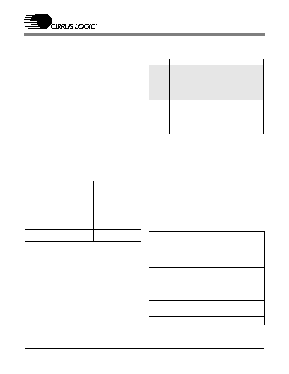
81
input FIFO and may result in corrupted data
being heard on the outputs.
Corruption is only an issue when PCM data is
being delivered. When compressed data is
being
delivered,
there
are
sync
words
embedded in the data stream to which the DSP
can lock. Certain application codes that are
capable of processing PCM may now have a
special feature called "PCM Robustness"
which prevents the corruption described above,
but you should still use a FIFO reset to ensure
good data.
11.5 Serial Audio Input
The Serial Audio Input (SAI) provides four stereo
inputs to DSPC. The SAI can be used to post-
process PCM data from a multichannel Super
Audio CD input or DVD Audio/Video input via
high-performance A/Ds.
Table 19
shows the
mnemonic, pin name and pin number of the pins
associated with the SAI port on the CS49400.
The SAI has 4 stereo data inputs that are fully
configurable including support for I
2
S, left-
justified and multichannel formats. The SAI port
operates in slave mode only with LRCLKN and
SCLKN as inputs. Processing on the CDI and DAI
ports must be disabled before the SAI port is
enabled. Either the input D0 or D1 message must
be sent to DSPC to configure and enable the SAI
port.
11.6 Digital Audio Output Port
The Digital Audio Output port (DAO) can transmit
up to 16 channels of PCM data that are fully
configurable into standard audio format. It also has
two IEC60958 pins that provide CMOS level bi
phase encoded outputs.
Table 25
shows the signals
associated with the DAO. As with the input ports
the clocks and data are fully configurable via
hardware configuration. All DAO configuration
messages must be sent to DSPC.
Pin Name
Pin Description
144-Pin
Package,
Pin
Number
100-Pin
Package,
Pin
Number
SCLKN
Serial Bit Clock
86
60
LRCLKN
Frame Clock
85
59
SDATAN3
Serial Data In 3
79
55
SDATAN2
Serial Data In 2
80
56
SDATAN1
Serial Data In 1
81
57
SDATAN0
Serial Data In 0
82
58
Table 23. Serial Audio Input Port
D Value
Data Type
Hex Message
0
PCM - I
2
S 24-bit
0x81000010
0x00000001
0x81000011
0x00011701
0x81000012
0x00004E4F
1
PCM - Left Justified 24-bit
0x81000010
0x00000001
0x81000011
0x00001600
0x81000012
0x00005E4F
Table 24. SAI Data Type Configuration
(Input Parameter D)
Pin Name
Pin Description
144-Pin
Number
100-Pin
Number
MCLK
Master Clock
99
68
SCLK1
Serial Bit Clock for
AUDATA 4-7
98
67
LRCLK1
Frame Clock for
AUDATA 4-7
87
61
AUDATA7,X
MT958B
Serial Data Out 7,
IEC60958 Trans-
mitter
92
64
AUDATA6
Serial Data Out 6
93
65
AUDATA5
Serial Data Out 5
94
66
AUDATA4
Serial Data Out 4
102
71
Table 25. Digital Audio Output Port

82
MCLK is the master clock and is firmware
configurable to be either an input or an output. If
MCLK is to be used as an output, the internal PLL
must be used. As an output MCLK can be
configured to provide a 128Fs, 256Fs, or 512Fs
clock, where Fs is the output sample rate.
SCLK0 is the bit clock used to clock data out on
AUDATA0,
AUDATA1,
AUDATA2
and
AUDATA3. LRCLK0 is the data framing clock
whose frequency is typically equal to the sampling
frequency
for
AUDATA0,
AUDATA1,
AUDATA2 and AUDATA3.
SCLK1 is the bit clock used to clock data out on
AUDATA4,
AUDATA5,
AUDATA6
and
AUDATA7. LRCLK1 is the data framing clock
whose frequency is typically equal to the sampling
frequency
for
AUDATA4,
AUDATA5,
AUDATA6 and AUDATA7.
LRCLK0, LRCLK1, SCLK0 and SCLK1 can be
configured as either inputs (Slave) or outputs
(Master). A valid MCLK is required for all output
modes. When LRCLK0, LRCLK1, SCLK0 and
SCLK1 are configured as outputs, they are derived
from MCLK. Whether MCLK is configured as an
input or an output, an internal divider from the
MCLK signal is used to produce LRCLK0,
LRCLK1, SCLK0 and SCLK1. The ratios shown
in
Table 26
give the possible SCLK values for
different MCLK frequencies. (All values are
expressed in terms of the sampling frequency, Fs.)
Both the AUDAT0 and AUDAT4 Digital Audio
Output porst are configurable to provide output for
two, four, or six channels of PCM data.
AUDATA1,
AUDATA2,
AUDATA3,
AUDATA5, AUDATA6 and AUDATA7 are only
capable of outputting two channels of PCM data.
Typically AUDATA[0:7] are configured for
outputting either left justified or I
2
S formatted data.
In a standard 5.1 channel AVR, AUDATA0,
AUDATA1 and AUDATA2 are used to output the
six discrete channels (Left, Center, Right, Left
Surround, Right Surround, and Subwoofer).
AUDATA3
can
be
used
with
AUDATA0,
AUDATA1 and AUDATA2 to support 7.1 output.
Alternatively AUDATA3 and AUDATA7 can be
used for dual zone support. AUDATA3 and
AUDATA7 are multiplexed with the XMT958
output so only one can be used at any one time.
Please
refer
to
AN208,
AN209
and
their
corresponding appendices for information about
which output modes are supported, as this is
specific to each application code.
11.6.1 S/PDIF Outputs
Both AUDATA3 and AUDATA7 digital audio
output ports are unique, in that they can serve either
an additional output for I2S or Left Justified PCM
data OR as IEC60959 bi-phase mark encoded data
S/PDIF transmitters. When either of these ports are
configured as a S/PDIF transmitter, the MCLK
required for such functionality can be provided
from either the internally locked PLL or from an
SCLK0
Serial Bit Clock for
AUDATA 0-3
104
72
LRCLK0
Frame Clock for
AUDATA 0-3
108
75
AUDATA3,X
MT958A
Serial Data Out 3,
IEC60958 Trans-
mitter
106
73
AUDATA2
Serial Data Out 2
107
74
AUDATA1
Serial Data Out 1
109
76
AUDATA0
Serial Data Out 0
110
77
Pin Name
Pin Description
144-Pin
Number
100-Pin
Number
Table 25. Digital Audio Output Port (Continued)
MCLK
(Fs)
SCLK (Fs)
32
48
64
128
256
512
128
X
X
384
X
X
X
256
X
X
X
X
512
X
X
X
X
X
Table 26. MCLK/SCLK Master Mode Ratios
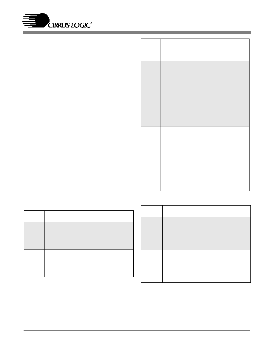
83
MCLK
input. All consumer channel status
information can be included in the S/PDIF stream,
provided that the particular application code
supports this functionality.
When configured as a S/PDIF transmitter, the
designer should understand that in order for these
ports to be fully IEC60958 compliant, the outputs
would need to be buffered through an RS422
device or an optocoupler as its outputs are only
CMOS driven.
11.7 Output Data Hardware Configuration
The DAO naming convention is as follows:
OUTPUT A B C D,
where the parameters are defined as:
A - DAO Mode (Master/Slave for LRCLK0,
LRCLK1, SCLK0 and SCLK1)
B - Data Format
C - MCLK, SCLK, LRCLK Frequency
The following tables show the different values for
each parameter as well as the hex message that
needs to be sent. When creating the hardware
configuration message, only one hex message
should be sent per parameter.
A
Value
DAO Modes (LRCLK and
SCLK)
Hex Message
0
(default)
MCLK - Slave
SCLK0 - Slave
LRCLK0 - Slave
SCLK1 - Slave
LRCLK1 - Slave
0x81800003
0x00101000
1
MCLK - Slave
SCLK0 - Master
LRCLK0 - Master
SCLK1 - Master
LRCLK1 - Master
0x81800003
0xFFEFFFFF
Table 27. Output Clock Configuration
(Parameter A)
B
Value
DAO Data Format Of
AUDATA0, 1, 2 (or
AUDATA0 for Multichannel
Modes)
Hex
Message
0
(default)
I
2
S 24-bit
(Configuration of AUDATA3 as
S/PDIF (IEC60958) or Digital Audio
in the format of I
2
S or Left Justified is
covered in AN209)
0x81800003
0xFFFE3FFF
0x81400003
0x0001C000
0x81000005
0x00101701
0x81000006
0x00100001
0x81000007
0x00100001
0x81000008
0x00100001
1
Left Justified 24-bit
(Configuration of AUDATA3 as
S/PDIF (IEC60958) or Digital Audio
in the format of I
2
S or Left Justified is
covered in AN209)
0x81800003
0xFFFE3FFF
0x81400003
0x0000C000
0x81000005
0x00101701
0x81000006
0x00100000
0x81000007
0x00100000
0x81000008
0x00100000
Table 28. Output Data Configuration Parameter B)
C Value
SCLK/LRCLK Frequency
Hex
Message
0
(default)
MCLK = 256 FS
SCLK = MCLK / 4 = 64 FS
LRCLK = SCLK / 64 = FS
0x81800003
0xFFFFFC7F
0x81400003
0x00000100
0x81000009
0x00077030
1
MCLK = 256 FS
SCLK = MCLK / 2 = 128 FS
LRCLK = SCLK / 128 = FS
0x81800003
0xFFFFFC7F
0x81400003
0x00000200
0x81000009
0x00177010
Table 29. Output SCLK/LRCLK Configuration
(Parameter C)
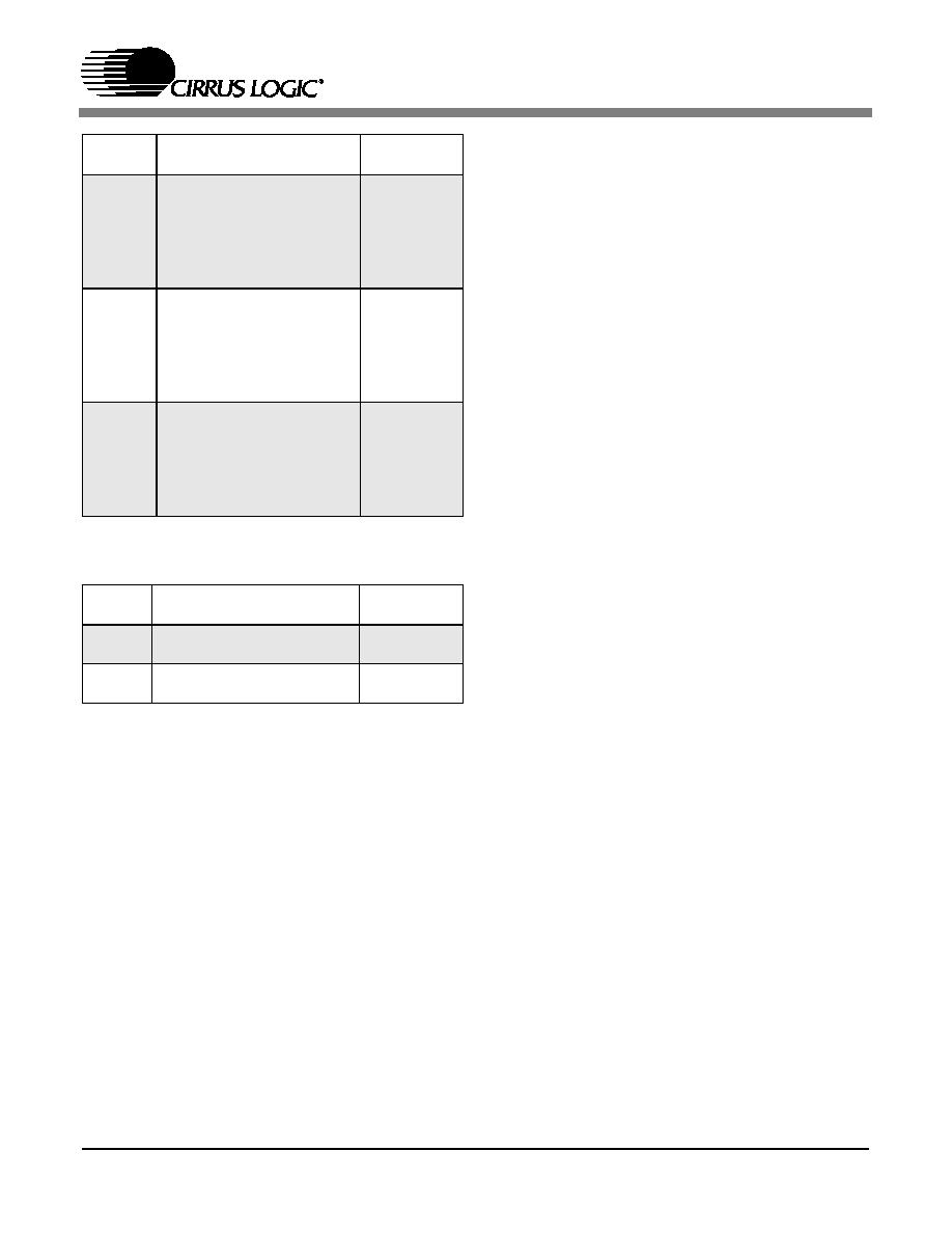
84
11.8 Creating Hardware Configuration
Messages
The single hardware configuration message that
must be sent to the CS49400 after download or soft
reset should be a concatenation of the messages in
the previous sections. The complete hardware
configuration message should be created by taking
a message for each parameter (where the default is
not acceptable) and concatenating the messages
together. No messages need to be sent if the default
configuration
for
a
particular
parameter
is
acceptable. This example can be easily expanded to
fit other system requirements.
E.g. if the host system has this configuration:
Address Checking: Disabled
This
is
the
default
configuration
so
no
configuration message is required.
DAI:Left Justified
PCM and Compressed data
CDI:Not used
The above configuration corresponds to
INPUT A1 B1
which corresponds to a configuration message of:
0x800210
0x3FBFC0
0x800110
0xC0002C
0x800217
0x8080FF
0x80021A
0x8080FF
0x800117
0x001000
0x80011A
0x001800
DAO:Left Justified slave mode (LRCLK,
SCLK inputs)
MCLK @ 256Fs
SCLK @ 64Fs
The above configuration corresponds to
OUTPUT A0 B1 C0 D0
which has a configuration message of:
0x81800003
0xFFFE3FFF
0x81400003
0x0000C000
0x81000005
0x00101701
0x81000006
0x00100000
0x81000007
2
MCLK = 256 FS
SCLK = MCLK / 1 = 256 FS
LRCLK = SCLK / 256 = FS
0x81800003
0xFFFFFC7F
0x81400003
0x00000300
0x81000009
0x00377000
3
MCLK = 512 FS
SCLK = MCLK / 8 = 64 FS
LRCLK = SCLK / 64 = FS
0x81800003
0xFFFFFC7F
0x81400003
0x00000100
0x81000009
0x00077070
4
MCLK = 128FS
SCLK = MCLK / 2 = 64FS
LRCLK = SCLK / 64 = FS
0x81800003
0xFFFFFC7F
0x81400003
0x00000100
0x81000009
0x00077010
D Value
SCLK Polarity
Hex
Message
0
(default)
Data Valid on Rising Edge
(clocked out on falling)
0x81800003
0xFFFBFFFF
1
Data Valid on Falling Edge
(clocked out on rising)
0x81400003
0x00040000
Table 30. Output SCLK Polarity Configuration
(Parameter D)
C Value
SCLK/LRCLK Frequency
Hex
Message
Table 29. Output SCLK/LRCLK Configuration
(Parameter C)
85
0x00100000
0x81000008
0x00100000
Concatenating the messages together gives the
hardware
configuration
message
shown
in
Table 31, "Example Values to be Sent to DSPAB
After Download or Soft Reset," on page 85, which
should be sent to DSPAB after download or soft
reset. Table 32, "Example Values to be Sent to
DSPC After Download or Soft Reset," on page 85,
which should be sent to DSPC after download or
soft reset.
WORD#
VALUE
WORD#
VALUE
1
0x800210
7
0x80021A
Table 31. Example Values to be Sent to DSPAB After
Download or Soft Reset
2
0x3FBFC0
8
0x8080FF
3
0x800110
9
0x800117
4
0xC0002C
10
0x001000
5
0x800217
11
0x80011A
6
0x8080FF
12
0x001800
WORD#
VALUE
WORD#
VALUE
1
0x81000006
12
0x81000007
2
0x00101700
13
0x00100000
3
0x81000006
14
0x81000008
4
0x00100000
15
0x00100000
Table 32. Example Values to be Sent to DSPC After
Download or Soft Reset
Table 31. Example Values to be Sent to DSPAB After
Download or Soft Reset
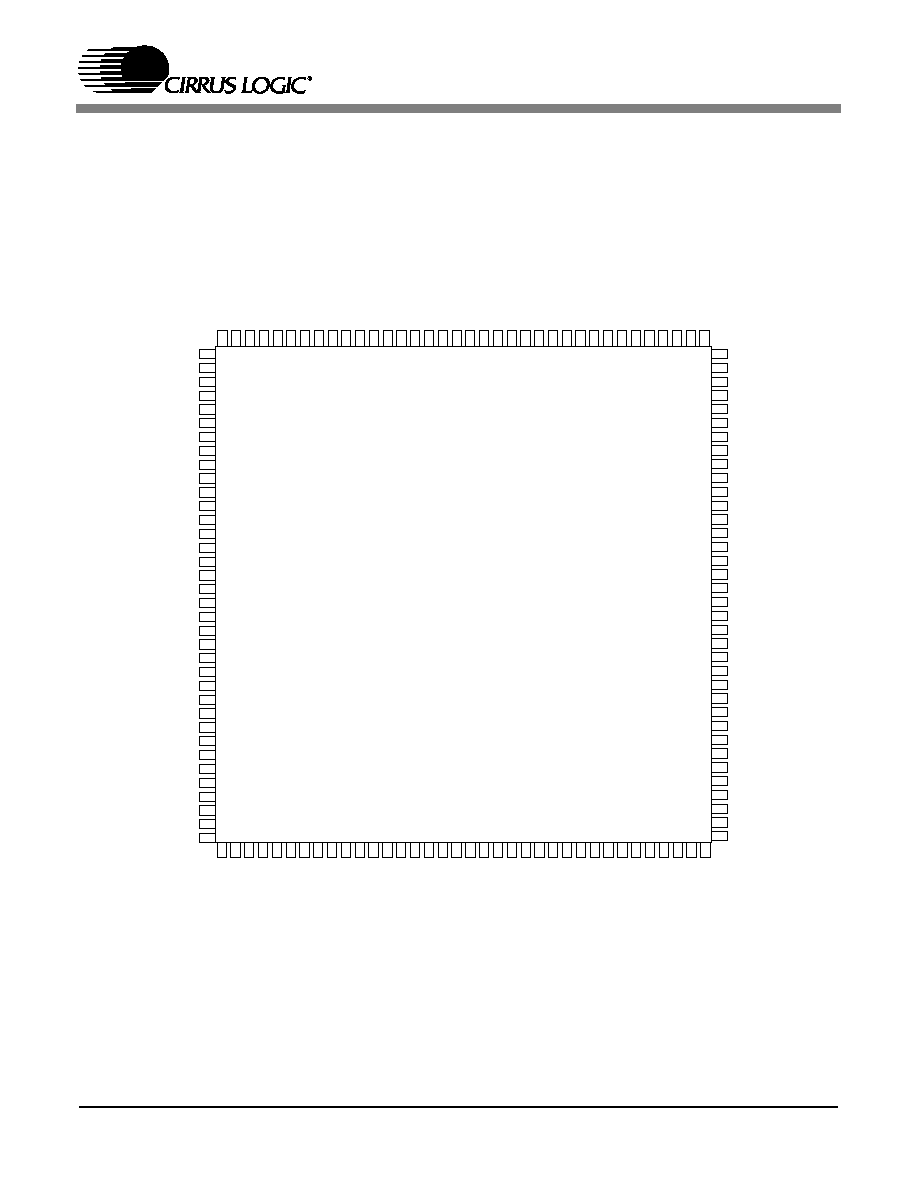
86
12.0 PIN DESCRIPTION
12.1 144-Pin LQFP Package Pin Layout
FILT1
FILT2
CLKIN, XTALI
XTALO
CLKSEL
FD
A
T
7
FD
A
T
6
FD
A
T
5
FD
A
T
4
FD
A
T
3
FD
A
T
2
FD
A
T
1
FD
A
T
0
F
A
O
,
FSCCLK
F
A
1, FSCDIN
FHS1,
FRD
, FR/
W
FHS0,
FWR
,
FDS
FCS
FHS2, FSCDIO
,
FSCDOUT
FINTREQ
FSCLKN1, STCCLK2
FLRCLKN1
FSDATAN1
CMPCLK, FSCLKN2
CMPDAT, FSDATAN2
FDBCK
FDBD
A
PLLVDD
PLLVSS
RESET
TEST
MCLK
SCLK0
SCLK1
LRCLK0
LRCLK1
AUDATA0
AUDATA1
A
U
D
ATA
2
A
U
D
A
T
A3, XMT958A
AU
D
A
T
A4, GPIO28
A
U
D
A
T
A5, GPIO29
A
U
D
A
T
A6, GPIO30
A
U
D
A
T
A7, XMT958B
, GPIO31
DBCK
DBD
A
SCLKN, GPIO22
LRCLKN, GPIO23
SD
A
T
AN0, GPIO24
SD
A
T
A
N1, GPIO25
SD
A
T
A
N2, GPIO26
SD
A
T
A
N3, GPIO27
SCS
SCCLK
SCDIN
SCDOUT, SCDIO
INTREQ
HD
A
T
A7, GPIO7
HD
A
T
A6, GPIO6
HD
A
T
A5, GPIO5
HD
A
T
A4, GPIO4
HD
A
T
A3, GPIO3
HDATA2, GPIO2
HDATA1, GPIO1
HDATA0, GPIO0
A0, GPIO13
A1, GPIO12
SD_ADDR8, EXTA8
SD_ADDR7, EXTA7
SD_ADDR6, EXTA6
SD_ADDR5, EXTA5
SD_ADDR4, EXTA4
SD_ADDR3 ,EXT
A3
SD_ADDR2 ,EXT
A2
SD_ADDR1 ,EXT
A1
SD_ADDR0, EXT
A0
SD_CLK_OUT
SD_CLK_IN
SD_DATA8, EXTA11
SD_DATA7, EXTD7
SD_DATA6, EXTD6
SD_DATA5, EXTD5
SD_DATA4, EXTD4
SD_DATA3, EXTD3
SD_D
A
T
A
2, EXTD2
SD_D
A
T
A1, EXTD1
SD_D
A
T
A0, EXTD0
SD_ADDR10, EXTA10
SD_ADDR9, EXTA9
RD, R/W, GPIO11
WR, DS, GPIO10
CS, GPIO9
HINBSY, GPIO8
SD_DATA15, EXTA18
SD_DATA14, EXTA17
SD_DATA13, EXTA16
SD_DATA12, EXTA15
SD_DATA11, EXTA14
SD_DATA10, EXTA13
SD_DATA9, EXTA12
UHS2,
CS_OUT, GPIO17
UHS0, GPIO18
UHS1, GPIO19
GPIO20
GPIO21
VDD4
VDD7
VDD1
VDD3
VSS4
VSS
7
VSS1
VSS3
VDD6
VDD2
VDD5
VSS6
VSS2
VSS5
VDDSD1
VDDSD2
VDDSD3
SD_CLK_EN
SD_BA, EXTA19
SD_CS
SD_RAS
SD_CAS
SD_WE
SD_DQM1
SD_DQM0
NV_CS
, GPIO14
NV_OE
, GPIO15
NV_W
E
, GPIO16
VDDSD4
VSSSD1
VSSSD2
VSSSD3
VSSSD4
NC1
NC2
NC3
NC4
NC5
CMPREQ, FLRCLKN2
1
5
10
15
20
25
30
40
45
50
55
60
65
70
75
80
85
90
95
100
105
115
110
120
125
130
135
140
144
35
Figure 57. Pin Layout (144-Pin LQFP Package)

87
12.2 100-Pin LQFP Package Pin Layout
20
1
5
10
15
25
30
35
55
50
40
45
60
65
75
70
80
85
90
95
100
UHS0
,
GPI
O
1
8
IN
T
R
E
Q
UHS1
,
GPI
O
1
9
FA
1
,
FS
C
D
I
N
FA
0,
FS
C
C
L
K
VDDSD4
F
I
NT
REQ
FC
S
FH
S
0
,
F
WR
,
F
D
S
VDD6
F
H
S2
,
F
SCDI
O,
F
S
CDOUT
VS
S6
F
H
S1
,
F
RD,
F
R
/
W
FD
B
D
A
VDD7
FD
B
C
K
VS
S7
TE
ST
DBDA
DBCK
LR
C
L
K
1
EX
TD0
NV_
W
E
,
GPI
O
1
6
NV_
O
E
,
GPI
O
1
5
NV_
C
S
,
GPI
O
1
4
EX
TD1
EX
TD2
SC
L
K
1
EXTA19
VSSSD1
AU
D
A
T
A
7
,
X
M
T9
5
8
B,
G
P
I
O
3
1
AU
D
A
T
A
2
SD
A
T
AN
3
,
G
P
IO
2
7
EXTA9
EXTD7
EXTD6
EXTD4
EXTA18
VSSSD4
EXTD5
EXTD3
EXTA17
EXTA16
EXTA15
EXTA14
EXTA13
EXTA12
EXTA11
EXTA8
EXTA7
EXTA6
EXTA5
EXTA4
VDDSD1
EXTA10
EX
T
A
0
EX
T
A
1
EX
T
A
2
EX
T
A
3
SD
A
T
AN
2
,
G
P
IO
2
6
SD
A
T
AN
1
,
G
P
IO
2
5
SD
A
T
AN
0
,
G
P
IO
2
4
LR
C
L
K
N
,
G
P
I
O
2
3
S
C
LK
N
,
G
P
I
O
22
VD
D
1
V
SS1
A
U
D
A
TA
6,
G
P
I
O
30
A
U
D
A
TA
5,
G
P
I
O
29
A
U
D
A
TA
4,
G
P
I
O
28
MC
L
K
AU
D
A
T
A
3
,
XM
T9
5
8
A
SC
L
K
0
VD
D
2
V
SS2
LR
C
L
K
0
AUDATA1
CMPCLK, FSCLKN2
AUDATA0
CMPREQ, FLRCLKN2
CMPDAT, FSDATAN2
FSCLKN1, STCCLK2
FSDATAN1
VSS3
VDD3
FLRCLKN1
CLKSEL
PLLVSS
PLLVDD
FILT2
FILT1
XTALO
CLKIN, XTALI
SCS
SCDIN
VSS5
VDD5
SCDOUT, SCDIO
SCCLK
UHS2, CS_OUT, GPIO17
RESET
Figure 58. Pin Layout (100-Pin LQFP Package)

88
12.3 Pin Definitions
FILT1 -- Phase-Locked Loop Filter
Connects to an external filter for the on-chip phase-locked loop.
FILT2 -- Phase Locked Loop Filter
Connects to an external filter for the on-chip phase-locked loop.
CLKIN, XTALI -- External Clock Input/Crystal Oscillator Input
CS49400 clock input. This pin accepts an external clock input signal that is used to drive the
internal core logic. When in internal clock mode (CLKSEL == VSS), this input is connected to
the internal PLL from which all internal clocks are derived. When in external clock mode
(CLKSEL == VDD), this input is connected to the DSP clock. Alternatively, a 12.288 mhZ
crystal oscillator can be connected between XTALI and XTALO. INPUT
XTALO -- Crystal Oscillator Output
Crystal oscillator output. OUTPUT
CLKSEL -- DSP Clock Select
This pin selects the internal source clock. When CLKSEL is low, CLKIN is connected to the
internal PLL from which all internal clocks are derived. When CLKSEL is high, the PLL is
bypassed and the external clock directly drives all input logic. INPUT
FDAT7 -- DSPAB Bidirectional Data Bus
FDAT6
FDAT5
FDAT4
FDAT3
FDAT2
FDAT1
FDAT0
In parallel host mode, these pins provide a bidirectional data bus to DSPAB. These pins have
an internal pull-up.
BIDIRECTIONAL - Default: INPUT
FA0, FSCCLK -- Host Parallel Address Bit Zero or Serial Control Port Clock
In parallel host mode, this pin serves as one of two address input pins used to select one of
four parallel registers. In serial host mode, this pin serves as the serial control clock signal,
specifically as the SPI clock input. INPUT

89
FA1, FSCDIN -- Host Address Bit One or SPI Serial Control Data Input
In parallel host mode, this pin serves as one of two address input pins used to select one of
four parallel registers. In SPI serial host mode, this pin serves as the data input. INPUT
FHS1, FRD, FR/W -- Mode Select Bit 1 or Host Parallel Output Enable or Host Parallel R/W
DSPAB control port mode select bit 1. This bit is one of 3 control port select bits that are
sampled on the rising edge of RESET to determine the control port mode of DSPAB. In Intel
parallel host mode, this pin serves as the active-low data bus enable input. In Motorola parallel
host mode, this pin serves as the read-high/write-low control input signal. In serial host mode,
this pin can serve as the external memory active-low data-enable output signal.
BIDIRECTIONAL - Default: INPUT
FHS0, FWR, FDS -- Mode Select Bit 0 or Host Write Strobe or Host Data Strobe
DSPAB control port mode select bit 0. This bit is one of 3 control port select bits that are
sampled on the rising edge of RESET to determine the control port mode of DSPAB. In Intel
parallel host mode, this pin serves as the active-low data-write-input strobe. In Motorola
parallel host mode, this pin serves as the active-low data-strobe-input signal. In serial host
mode, this pin can serve as the external-memory active-low write-enable output signal.
BIDIRECTIONAL - Default: INPUT
FCS -- Host Parallel Chip Select, Host Serial SPI Chip Select
In parallel host mode, this pin serves as the active-low chip-select input signal. In serial host
SPI mode, this pin is used as the active-low chip-select input signal. INPUT
FHS2, FSCDIO, FSCDOUT -- Mode Select Bit 2 or Serial Control Port Data Input and Output, Par-
allel Port Type Select
DSPAB control port mode select bit 2. This bit is one of 3 control port select bits that are
sampled on the rising edge of RESET to determine the control port mode of DSPAB. In SPI
mode this pin serves as the data output pin. In parallel host mode, this pin is sampled at the
rising edge of RESET to configure the parallel host mode as an Intel type bus or as a
Motorola type bus. BIDIRECTIONAL - Default: INPUT
FINTREQ -- Control Port Interrupt Request
Open-drain interrupt-request output. This pin is driven low to indicate that the DSP has
outgoing control data that should be read by the host.
OPEN DRAIN I/O - Requires 3.3K Ohm Pull-Up
FSCLKN1, STCCLK2
--
PCM Audio Input Bit Clock
Digital-audio bit clock input. FSCLKN1 operates asynchronously from all other DSPAB clocks.
In master mode, FSCLKN1 is derived from DSPAB
's
internal clock generator. The active edge
of FSCLKN1 can be programmed by the DSP.
BIDIRECTIONAL - Default: INPUT
FLRCLKN1 -- PCM Audio Input Sample Rate Clock

90
Digital-audio frame clock input. FLRCLKN1 typically is run at the sampling frequency.
FLRCLKN1 operates asynchronously from all other DSPAB clocks. The polarity of FLRCLKN1
for a particular subframe can be programmed by the DSP.
BIDIRECTIONAL - Default: INPUT
FSDATAN1 -- PCM Audio Data Input One
Digital-audio data input that can accept from one compressed line or 2 channels of PCM data.
FSDATAN1 can be sampled with either edge of FSCLKN1, depending on how FSCLKN1 has
been configured. INPUT
CMPCLK, FSCLKN2 -- PCM Audio Input Bit Clock
Digital-audio bit clock input. FSCLKN2 operates asynchronously from all other DSPAB clocks.
The active edge of FSCLKN2 can be programmed by the DSP.
BIDIRECTIONAL - Default: INPUT
CMPDAT, FSDATAN2 -- PCM Audio Data Input Number Two
Digital-audio data input that can accept either one compressed line or 2 channels of PCM
data. FSDATAN2 can be sampled with either edge of FSCLKN2, depending on how FSCLKN2
has been configured.
BIDIRECTIONAL - Default: INPUT
FDBCK -- Reserved
This pin is reserved and should be pulled up with an external 3.3k resistor. INPUT
FDBDA -- Reserved
This pin is reserved and should be pulled up with an external 3.3k resistor.
BIDIRECTIONAL - Default: INPUT
PLLVDD -- PLL Supply Voltage
2.5 V PLL supply.
PLLVSS -- PLL Ground Voltage
PLL ground.
RESET -- Master Reset Input
Asynchronous active-low master reset input. Reset should be low at power-up to initialize the
DSP and to guarantee that the device is not active during initial power-on stabilization periods.
At the rising edge of reset the host interface mode of DSPAB is selected contingent on the
state of the FHS0, FHS1, and FHS2 pins. At the rising edge of reset the host interface mode
of DSPC is selected contingent on the state of the UHSO, UHS1, and UHS2 pins. If reset is
low all bidirectional pins are high-Z inputs. INPUT
TEST -- Reserved

91
This should be tied low for normal operation. INPUT
MCLK -- Audio Master Clock
Bidirectional master audio clock. As an output, MCLK provides a low jitter oversampling clock.
MCLK supports all standard oversampling frequencies. BIDIRECTIONAL - Default: INPUT
SCLK0 -- Audio Output Bit Clock
Bidirectional digital-audio output bit clock for AUDATA0, AUDATA1, AUDATA2, and AUDATA3.
As an output, SCLK0 can provide 32 Fs, 64 Fs, 128 Fs, 256 Fs, or 512 Fs frequencies and is
synchronous to MCLK. As an input, SCLK0 is independent of MCLK.
BIDIRECTIONAL - Default: INPUT
SCLK1 -- Audio Output Bit Clock
Bidirectional digital-audio output bit clock for AUDATA4, AUDATA5, AUDATA6, and AUDATA7.
As an output, SCLK1 can provide 32 Fs, 64 Fs, 128 Fs, 256 Fs, or 512 Fs frequencies and is
synchronous to MCLK. As an input, SCLK1 is independent of MCLK.
BIDIRECTIONAL - Default: INPUT
LRCLK0 -- Audio Output Sample Rate Clock
Bidirectional digital-audio output frame clock for AUDATA0, AUDATA1, AUDATA2, and
AUDATA3. As an output, LRCLK0 can provide all standard output sample rates up to 192 kHz
and is synchronous to MCLK. As an input, LRCLK0 is independent of MCLK.
BIDIRECTIONAL - Default: INPUT
LRCLK1 -- Audio Output Sample Rate Clock
Bidirectional digital-audio output frame clock for AUDATA4, AUDATA5, AUDATA6, and
AUDATA7. As an output, LRCLK1 can provide all standard output sample rates up to 192 kHz
and is synchronous to MCLK. As an input, LRCLK1 is independent of MCLK.
BIDIRECTIONAL - Default: INPUT
AUDATA0 -- Digital Audio Output 0
PCM digital-audio data output. OUTPUT
AUDATA1 -- Digital Audio Output 1
PCM digital-audio data output. OUTPUT
AUDATA2 -- Digital Audio Output 2
PCM digital-audio data output. OUTPUT
AUDATA3, XMT958A -- Digital Audio Output 3, S/PDIF Transmitter

92
CMOS level output that outputs a biphase-mark encoded (S/PDIF) IEC60958 signal or digital
audio data which is capable of carrying two channels of PCM digital audio. OUTPUT
AUDATA4, GPIO28 -- Digital Audio Output 4, General Purpose I/O
PCM digital-audio data output. This pin can act as a general-purpose input or output that can
be individually configured and controlled by DSPC. BIDIRECTIONAL - Default: OUTPUT
AUDATA5, GPIO29 -- Digital Audio Output 5, General Purpose I/O
PCM digital-audio data output. This pin can act as a general-purpose input or output that can
be individually configured and controlled by DSPC. BIDIRECTIONAL - Default: OUTPUT
AUDATA6, GPIO30 -- Digital Audio Output 6, General Purpose I/O
PCM digital-audio data output. This pin can act as a general-purpose input or output that can
be individually configured and controlled by DSPC. BIDIRECTIONAL - Default: OUTPUT
AUDATA7, XMT958B, GPIO31 -- Digital Audio Output 7, S/PDIF Transmitter, General Purpose I/O
CMOS level output that contains a biphase-mark encoded (S/PDIF) IEC60958 signal or digital
audio data which is capable of carrying two channels of PCM digital audio. This pin can also
act as a general-purpose input or output that can be individually configured and controlled by
DSPC. BIDIRECTIONAL - Default: OUTPUT
DBCK -- Debug Clock
Must be tied high to 3.3k ohm resistor. INPUT
DBDA -- Debug Data
Must be tied high to 3.3k ohm resistor. BIDIRECTIONAL - Default: INPUT
SLCKN, GPIO22 -- PCM Audio Input Bit Clock, General Purpose I/O
Digital-audio bit clock that is an input. SCLKN operates asynchronously from all other DSPAB
clocks. The active edge of SCLKN can be programmed by the DSP. This pin can act as a
general-purpose input or output that can be individually configured and controlled by DSPC.
BIDIRECTIONAL - Default: INPUT
LRCLKN, GPIO23 -- PCM Audio Input Sample Rate Clock, General Purpose I/O
Digital-audio frame clock input. LRCLKN operates asynchronously from all other DSPAB
clocks. The polarity of LRCLKN for a particular subframe can be programmed by the DSP.
This pin can act as a general-purpose input or output that can be individually configured and
controlled by DSPC. BIDIRECTIONAL - Default: INPUT
SDATAN0, GPIO24 -- PCM Audio Input Data, General Purpose I/O
Digital-audio PCM data input. This pin can act as a general-purpose input or output that can
be individually configured and controlled by DSPC. BIDIRECTIONAL - Default: INPUT
SDATAN1, GPIO25 -- PCM Audio Input Data, General Purpose I/O

93
Digital-audio PCM data input. This pin can act as a general-purpose input or output that can
be individually configured and controlled by DSPC. BIDIRECTIONAL - Default: INPUT
SDATAN2, GPIO26 -- PCM Audio Input Data, General Purpose I/O
Digital-audio PCM data input. This pin can act as a general-purpose input or output that can
be individually configured and controlled by DSPC. BIDIRECTIONAL - Default: INPUT
SDATAN3, GPIO27 -- PCM Audio Input Data, General Purpose I/O
Digital-audio PCM data input. This pin can act as a general-purpose input or output that can
be individually configured and controlled by DSPC. BIDIRECTIONAL - Default: INPUT
SCS -- Host Serial SPI Chip Select
SPI mode active-low chip-select input signal. INPUT
SCCLK -- Serial Control Port Clock
This pin serves as the serial SPI clock input. INPUT
SCDIN -- SPI Serial Control Data Input
In SPI mode this pin serves as the data input pin. INPUT
SCDOUT, SCDIO -- Serial Control Port Data Input and Output
In SPI mode this pin serves as the data output pin. BIDIRECTIONAL - Default: OUTPUT in
SPI mode
INTREQ -- Control Port Interrupt Request
Open-drain interrupt-request output. This pin is driven low to indicate that DSPC has outgoing
control data and should be serviced by the host.
OPEN DRAIN I/O - Requires 3.3K Ohm Pull-Up

94
HDATA7, GPIO7 -- DSPC Bidirectional Data Bus, General Purpose I/O
HDATA6, GPIO6
HDATA5, GPIO5
HDATA4, GPIO4
HDATA3, GPIO3
HDATA2, GPIO2
HDATA1, GPIO1
HDATA0, GPIO0
In parallel host mode, these pins provide a bidirectional data bus. These pins can also act as
general purpose input or output pins that can be individually configured and controlled by
DSPC. These pins have an internal pull-up. BIDIRECTIONAL - Default: INPUT
A0, GPIO13
--
Host Parallel Address Bit 0, General Purpose I/O
In parallel host mode, this pin serves as the LS Bit of a two bit address input used to select
one of four parallel registers. This pin can act as a general-purpose input or output that can be
individually configured and controlled by DSPC. BIDIRECTIONAL - Default: INPUT
A1, GPIO12 -- Host Address Bit 1, General Purpose I/O
In parallel host mode, this pin serves as the MS Bit of a two bit address input used to select
one of four parallel registers. This pin can act as a general-purpose input or output that can be
individually configured and controlled by DSPC. BIDIRECTIONAL - Default: INPUT
RD, R/W, GPIO11 -- Host Parallel Output Enable, Host Parallel R/W, General Purpose I/O
In Intel parallel host mode, this pin serves as the active-low data bus enable input. In Motorola
parallel host mode, this pin serves as the read-high/write-low control input signal. This pin can
act as a general-purpose input or output that can be individually configured and controlled by
DSPC. This pin has an internal pull-up. BIDIRECTIONAL - Default: INPUT
WR, DS, GPIO10
--
Host Write Strobe, Host Data Strobe, General Purpose I/O
In Intel parallel host mode, this pin serves as the active-low data bus enable input. In Motorola
parallel host mode, this pin serves as the read-high/write-low control input signal. In serial host
mode, this pin can serve as a general purpose input or output bit. This pin can act as a
general-purpose input or output that can be individually configured and controlled by DSPC.
This pin has an internal pull-up.
BIDIRECTIONAL - Default: INPUT
CS, GPIO9 -- Host Parallel Chip Select, General Purpose I/O
In parallel host mode, this pin serves as the active-low chip-select input signal. This pin can
act as a general-purpose input or output that can be individually configured and controlled by
DSPC. This pin has an internal pull-up. BIDIRECTIONAL - Default: INPUT

95
HINBSY, GPIO8 -- Input Host Message Status, General Purpose I/O
This pin indicates that serial or parallel communication data written to the DSP has not been
read yet. This pin can act as a general-purpose input or output that can be individually
configured and controlled by DSPC. This pin has an internal pull-up. BIDIRECTIONAL -
Default: OUTPUT
SD_DATA15, EXTA18 -- SDRAM Data Bus, SRAM External Address Bus
SD_DATA14, EXTA17
SD_DATA13, EXTA16
SD_DATA12, EXTA15
SD_DATA11, EXTA14
SD_DATA10, EXTA13
SD_DATA9, EXTA12
SD_DATA8, EXTA11
SDRAM data bus 15:8. SRAM external address bus 18:11. OUTPUT
SD_DATA7, EXTD7 -- SDRAM Data Bus, SRAM External Data Bus
SD_DATA6, EXTD6
SD_DATA5, EXTD5
SD_DATA4, EXTD4
SD_DATA3, EXTD3
SD_DATA2, EXTD2
SD_DATA1, EXTD1
SD_DATA0, EXTD0
SDRAM data bus 7:0. SRAM external data bus 7:0. BIDIRECTIONAL - Default: INPUT
SD_ADDR10, EXTA10 -- SDRAM Address Bus, SRAM External Address Bus
SD_ADDR9, EXTA9
SD_ADDR8, EXTA8
SD_ADDR7, EXTA7
SD_ADDR6, EXTA6
SD_ADDR5, EXTA5
SD_ADDR4, EXTA4
SD_ADDR3, EXTA3
SD_ADDR2, EXTA2
SD_ADDR1, EXTA1
SD_ADDR0, EXTA0
SDRAM address bus 10:0. SRAM external address bus 10:0. OUTPUT

96
SD_CLK_OUT -- SDRAM Clock Output
SDRAM clock output. OUTPUT
SD_CLK_IN -- SDRAM Re-timing Clock Input
SDRAM re-timing clock input. INPUT
SD_CLK_EN -- SDRAM Clock Enable
SDRAM clock enable. OUTPUT
SD_BA, EXTA19 -- SDRAM Bank Address Select, SRAM External Address Bus
SDRAM bank address select. SRAM external address bus 19. OUTPUT
SD_CS -- SDRAM Chip Select
SDRAM chip select. OUTPUT
SD_RAS -- SDRAM Row Address Strobe
SDRAM row address strobe. OUTPUT
SD_CAS -- SDRAM Column Address Strobe
SDRAM column address strobe. OUTPUT
SD_WE -- SDRAM Write Enable
SDRAM write enable. OUTPUT
SD_DQM1 -- SDRAM Data Mask 1
SDRAM data mask 1. OUTPUT
SD_DQM0 -- SDRAM Data Mask 2
SDRAM data mask 0. OUTPUT
NV_CS, GPIO14 -- SRAM Chip Select, General Purpose I/O
SRAM/Flash chip select. This pin can act as a general-purpose input or output that can be
individually configured and controlled by DSPC. BIDIRECTIONAL - Default: OUTPUT
NV_OE, GPIO15 -- SRAM Output Enable, General Purpose I/O
SRAM/Flash output enable. This pin can act as a general-purpose input or output that can be
individually configured and controlled by DSPC. BIDIRECTIONAL - Default: OUTPUT

97
NV_WE, GPIO16 -- SRAM Write Enable, General Purpose I/O
SRAM/Flash write enable. This pin can act as a general-purpose input or output that can be
individually configured and controlled by DSPC. BIDIRECTIONAL - Default: OUTPUT
UHS2, CS_OUT, GPIO17 -- Mode Select Bit 2, External Serial Memory Chip Select,
General Purpose I/O
DSPC control port mode select bit 2. This pin is sampled at the rising edge of RESET and is
one of three pins used to select the control port mode. In serial control port mode, this pin can
serve as an output to provide the chip-select for a serial EEPROM. This pin can act as a
general-purpose input or output that can be individually configured and controlled by DSPC.
BIDIRECTIONAL - Default: INPUT
UHS0, GPIO18 -- Mode Select Bit 0, General Purpose I/O
DSPC control port mode select bit 0. This pin is sampled at the rising edge of RESET and is
one of three pins used to select the control port mode. This pin can act as a general-purpose
input or output that can be individually configured and controlled by DSPC.
BIDIRECTIONAL - Default: INPUT
UHS1, GPIO19 -- Mode Select Bit 1, General Purpose I/O
DSPC control port mode select bit 1. This pin is sampled at the rising edge of RESET and is
one of three pins used to select the control port mode. This pin can act as a general-purpose
input or output that can be individually configured and controlled by DSPC.
BIDIRECTIONAL - Default: INPUT
GPIO20 -- General Purpose I/O
This pin can act as a general-purpose input or output that can be individually configured and
controlled by DSPC. This pin has an internal pull-up.
BIDIRECTIONAL - Default: INPUT
GPIO21 -- General Purpose I/O
This pin can act as a general-purpose input or output that can be individually configured and
controlled by DSPC.This pin has an internal pull-up.
BIDIRECTIONAL - Default: INPUT
VDD[7:1] -- 2.5V Supply Voltage
2.5V supply voltage.
VSS -- 2.5V Ground
2.5V ground.

98
NC[5:1] -- No Connect
Recommended tie to ground.
VDDSD[4:1] -- 3.3V SDRAM/SRAM/EPROM Interface Supply
3.3V SDRAM/SRAM/EPROM supply.
VSSSD -- 3.3V SDRAM/SRAM/EPROM Interface Ground
3.3V ground.
13. ORDERING INFORMATION
CS494002-CQ 144-pin, accommodates SRAM/SDRAM
CS494502-CQ 100-pin, external SRAM memory interface only (no SDRAM), no parallel-control ports, no
FLASH programming.
(Contact the factory for the 100-pin package pin-out and dimension drawing)
Temp Range 0-70∫ C for both parts

99
14. PACKAGE DIMENSIONS
14.1 144-Pin LQFP Package
INCHES
MILLIMETERS
DIM
MIN
NOM
MAX
MIN
A
---
0.55
0.063
---
A1
0.002
0.004
0.006
0.05
B
0.007
0.008
0.011
0.17
D
0.854
0.866 BSC
0.878
21.70
D1
0.783
0.787 BSC
0.791
19.90
E
0.854
0.866 BSC
0.878
21.70
E1
0.783
0.787 BSC
0.791
19.90
e
0.016
0.020
0.024
0.40
0.000∞
4∞
7.000∞
0.00∞
L
0.018
0.024
0.030
0.45
E1
E
D1
D
1
e
L
B
A1
A
Figure 59. 144-Pin LQFP Package Drawing
Note: See Legend Below