 | –≠–ª–µ–∫—Ç—Ä–æ–Ω–Ω—ã–π –∫–æ–º–ø–æ–Ω–µ–Ω—Ç: CS4953-CQ | –°–∫–∞—á–∞—Ç—å:  PDF PDF  ZIP ZIP |

Preliminary Product Information
This document contains information for a new product.
Cirrus Logic reserves the right to modify this product without notice.
1
Copyright
©
Cirrus Logic, Inc. 1997
(All Rights Reserved)
Cirrus Logic, Inc.
Crystal Semiconductor Products Division
P.O. Box 17847, Austin, Texas 78760
(512) 445 7222 FAX: (512) 445 7581
http://www.crystal.com
CS4952/53
NTSC/PAL Digital Video Encoder
Features
l
Simultaneous composite and S-video output
l
Supports RS170A and CCIR601 composite
output timing
l
Multi-standard support for NTSC-M, PAL (B, D,
G, H, I, M, N, Combination N)
l
Optional progressive scan @ MPEG2 field rates
l
CCIR656 input mode supporting EAV/SAV
codes and CCIR601 Master/Slave input modes
l
Stable color subcarrier for MPEG2 systems
l
NTSC closed caption encoder with interrupt
l
Supports Macrovision copy protection in
CS4953 version
l
Host interface configurable for parallel or I
2
C
compatible operation
l
General purpose input and output pins
l
Individual DAC power-down capability
l
On-chip voltage reference generator
l
On-chip color bar generator
l
+5 volt only, CMOS, low power modes, tri-state
DACs
Description
The CS4952/3 provides full conversion from YCbCr or
YUV digital video formats into NTSC & PAL Composite
and Y/C (S-video) analog video. Input formats can be
27 MHz 8-bit YUV, 8-bit YCbCr, or CCIR656 with sup-
port for EAV/SAV codes. Output video can be formatted
to be compatible with NTSC-M, or PAL B,D,G,H,I,M,N,
and Combination N systems. Also supported is NTSC
line 21 and line 284 closed captioning encoding.
Four 9-bit DACs provide two channels for an S-Video out-
put port and two composite video outputs. 2x oversampling
reduces the output filter requirements and guarantees
no DAC related modulation components within the spec-
ified bandwidth of any of the supported video standards.
Parallel or high speed I
2
C compatible control interfaces
are provided for flexibility in system design. The parallel
interface doubles as a general purpose I/O port when the
CS4952/3 is in I
2
C mode to help conserve valuable
board area.
ORDERING INFORMATION
CS4952/3-CL 44 pin PLCC
CS4952/3-CQ 44 pin TQFP
CLK
SCL
SDA
PDAT[7:0]
RD*
WR*
ADDR
XTAL
VD[7:0]
HSYNC*
VSYNC*
FIELD
INT
RESET*
C
CVBS37
CVBS75
Y
VREFIN
VREFOUT
ISET
VAA
GND
TEST
I C
Interface
2
Host
Parallel
Interface
Color Sub-carrier
Synthesizer
Video
Formatter
Video Timing
Generator
Control
Registers
Output
Interpolate
Chroma Amplifier
Chroma Modulate
Burst Insert
Chroma Interpolate
Luma Delay
Luma Amplifier
Sync Insert
9-Bit
DAC
Voltage
Reference
Current
Reference
8
8
LPF
LPF
Output
Interpolate
LPF
9-Bit
DAC
9-Bit
DAC
9-Bit
DAC
U, V
Y
OCT `97
DS223PP2

CS4952/53
2
DS223PP2
TABLE OF CONTENTS
AC & DC PARAMETRIC SPECIFICATIONS .....................................................................4
INTRODUCTION ...............................................................................................................11
FUNCTIONAL DESCRIPTION .........................................................................................11
Video Timing Generator .........................................................................................11
Video Input Formatter .............................................................................................11
Color Subcarrier Synthesizer ..................................................................................12
Chroma Path ..........................................................................................................12
Luma Path ..............................................................................................................12
Digital to Analog Converters ...................................................................................13
Voltage Reference ..................................................................................................13
Current Reference ..................................................................................................13
Host Interface .........................................................................................................13
Closed Caption Services ........................................................................................13
Control Registers ....................................................................................................13
OPERATIONAL DESCRIPTION .......................................................................................14
Reset Hierarchy ......................................................................................................14
Video Timing ...........................................................................................................14
Slave Mode Input Interface .............................................................................14
Master Mode Input Interface ...........................................................................14
Vertical Timing .................................................................................................15
Horizontal Timing ............................................................................................15
NTSC Interlaced ..............................................................................................17
PAL Interlaced .................................................................................................17
Progressive Scan ............................................................................................19
PAL Progressive Scan ....................................................................................19
NTSC Progressive Scan .................................................................................19
CCIR-656 ................................................................................................................19
Digital Video Input Modes .......................................................................................22
Multi-standard Output Format Modes .....................................................................22
Subcarrier Generation ............................................................................................22
Subcarrier Compensation .......................................................................................22
Closed Caption Insertion ........................................................................................23
Color Bar Generator ...............................................................................................23
Interrupts ................................................................................................................24
General Purpose I/O Port .......................................................................................24
ANALOG ...........................................................................................................................24
Analog Timing .........................................................................................................24
VREF ......................................................................................................................25
ISET ........................................................................................................................25
DACs ......................................................................................................................25
Luminance DAC ..............................................................................................25
Chrominance DAC ..........................................................................................25
CVBS75 DAC ..................................................................................................26
CVBS37 DAC ..................................................................................................26
PROGRAMMING ..............................................................................................................27
Host Control Interface .............................................................................................27
I2C Interface ....................................................................................................27
8-bit Parallel Interface .....................................................................................27
Register Description ...............................................................................................28
Control Register 0 ............................................................................................28
Control Register 1 ............................................................................................29
Control Register 2 ............................................................................................30
DAC Power Down Register ..............................................................................30
Status Register.................................................................................................31
Background Color Register ..............................................................................31
GPIO Control Register .....................................................................................31
GPIO Data Register .........................................................................................32
Chroma Filter Register .....................................................................................32
Luma Filter Register .........................................................................................32
I2C Address Register .......................................................................................32
Subcarrier Amplitude Register .........................................................................33

CS4952/53
DS223PP2
3
Subcarrier Synthesis Register ......................................................................... 33
Hue LSB Adjust Register ................................................................................. 33
Hue MSB Adjust Register ................................................................................ 33
Closed Caption Enable Register...................................................................... 34
Closed Caption Data Register ......................................................................... 34
Interrupt Enable Register ................................................................................. 34
Interrupt Clear Register.................................................................................... 35
Device ID Register ........................................................................................... 35
BOARD DESIGN & LAYOUT CONSIDERATIONS ......................................................... 36
Power and Ground Planes ..................................................................................... 36
Power Supply Decoupling ...................................................................................... 36
VREF Decoupling ................................................................................................... 36
Digital Interconnect ................................................................................................ 36
Analog Interconnect ............................................................................................... 37
Analog Output Protection ....................................................................................... 37
ESD Protection ....................................................................................................... 37
External DAC Output Filter ..................................................................................... 37
DEVICE PINOUT - 44 PLCC ............................................................................................ 38
PLCC Pin Description ............................................................................................ 39
DEVICE PINOUT - 44 TQFP ............................................................................................ 41
TQFP Pin Description ............................................................................................ 42
CS4952/53
4
DS223PP2
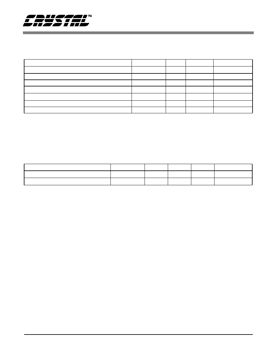
AC & DC PARAMETRIC SPECIFICATIONS
ABSOLUTE MAXIMUM RATINGS:
(AGND, DGND = 0 V, all voltages with respect to 0 V.)
Warning: Operating beyond these limits may result in permanent damage to the device.
Normal operation is not guaranteed at these extremes.
RECOMMENDED OPERATING CONDITIONS:
(AGND, DGND = 0 V, all voltages with
respect to 0 V.)
Parameter
Symbol
Min
Max
Units
Power Supply
V
AA
-0.3
6.0
V
Input Current Per Pin
Except Supply Pins
-10
10
mA
Output Current Per Pin
Except Supply Pins
-50
+50
mA
Analog Input Voltage
-0.3
V
AA
+0.3
V
Digital Input Voltage
-0.3
V
AA
+0.3
V
Ambient Temperature
Power Applied
-55
+125
∞C
Storage Temperature
-65
+150
∞C
Parameter
Symbol
Min
Typ
Max
Units
Power Supplies: Digital Analog
V
AA
4.75
5.0
5.25
V
Operating Ambient Temperature
T
A
0
+25
+70
∞C
CS4952/53
DS223PP2
5
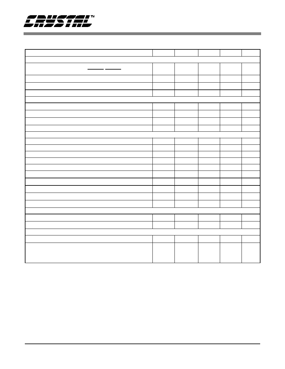
D.C. CHARACTERISTICS:
(T
A
=25 C; V
AA
= 5 V; GND = 0 V.)
Notes: 1. Output current levels with ISET = 10 k
, VREFIN = 1.232 V.
2. Times for black-to-white level and white-to-black level transitions.
Parameter
Symbol
Min
Typ
Max
Units
Digital Inputs
High Level Input Voltage
V [7:0], PDAT [7:0],
HSYNC/VSYNC/FIELD/CLKIN
V
IH
2.0
-
V
AA
+0.3
V
High Level Input Voltage
I
2
C
V
IH
0.7V
AA
-
-
V
Low Level Input Voltage
All Inputs
V
IL
-0.3
-
0.8
V
Input Leakage Current
Digital Inputs
-
-10
-
+10
µ
A
Digital Outputs
High Level Output Voltage
Io = -4mA
V
OH
2.4
-
V
AA
V
Low Level Output Voltage
Io = 4mA
V
OL
-
-
0.4
V
Low Level Output Voltage
SDA pin only, Io = 6mA
V
OL
-
-
0.4
V
Output Leakage Current
High-Z Digital Outputs
-
-10
-
+10
µ
A
Analog Outputs
Full Scale Output Current
CVBS37/Y/C (Note 1)
IO37
32.9
34.7
36.5
mA
Full Scale Output Current
CVBS75 (Note 1)
IO75
16.4
17.3
18.2
mA
LSB Current
CVBS37/Y/C (Note 1)
IB37
64.5
68
71.5
µ
A
LSB Current
CVBS75 (Note 1)
IB35
32.2
34
35.8
µ
A
DAC-to-DAC Matching
MAT
-
2
-
%
Output Compliance
V
OC
0
-
+1.4
V
Output Impedance
R
OUT
-
15
-
k
Output Capacitance
C
OUT
-
-
30
pF
DAC Output Delay
O
DEL
-
4
12
ns
DAC Rise/Fall Time
(Note 2)
T
RF
-
2.5
5
ns
Voltage Reference
Reference Voltage Output
V
OV
1.198
1.232
1.272
V
Reference Input Current
I
VC
-
-
10
µ
A
Power Supply
Supply Voltage
V
AA
4.75
5
5.25
V
Supply Current
All DACs on
CVBS75/CVGS37 only
CVBS75 only
I
AA
1
I
AA
2
I
AA
3
-
-
-
180
110
75
200
-
-
mA
mA
mA
CS4952/53
6
DS223PP2
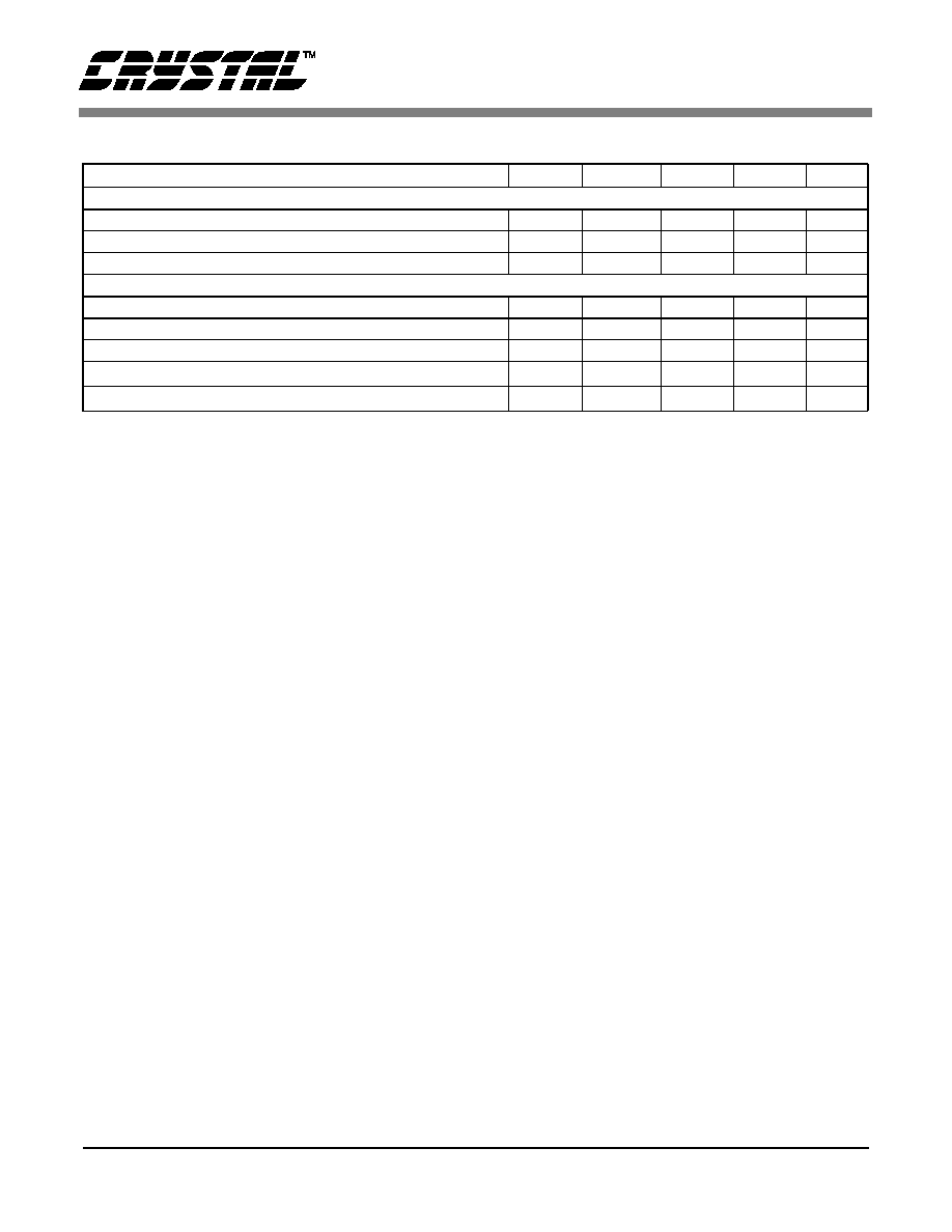
D.C. CHARACTERISTICS
(Continued)
Parameter
Symbol
Min
Typ
Max
Units
Static Performance
DAC Resolution
-
-
9
Bits
Differential Non-Linearity
DNL
-1
±0.5
+1
LSB
Integral Non-Linearity
INL
-1
±0.35
+1
LSB
Dynamic Performance
Differential Gain
DB
-
2
5
%
Differential Phase
DP
-
±0.5
±2
∞
Signal to Noise Ratio
SNR
-70
-
-
dB
Hue Accuracy
H
A
-
-
2
∞
Saturation Accuracy
S
A
-
-
2
%
CS4952/53
DS223PP2
7
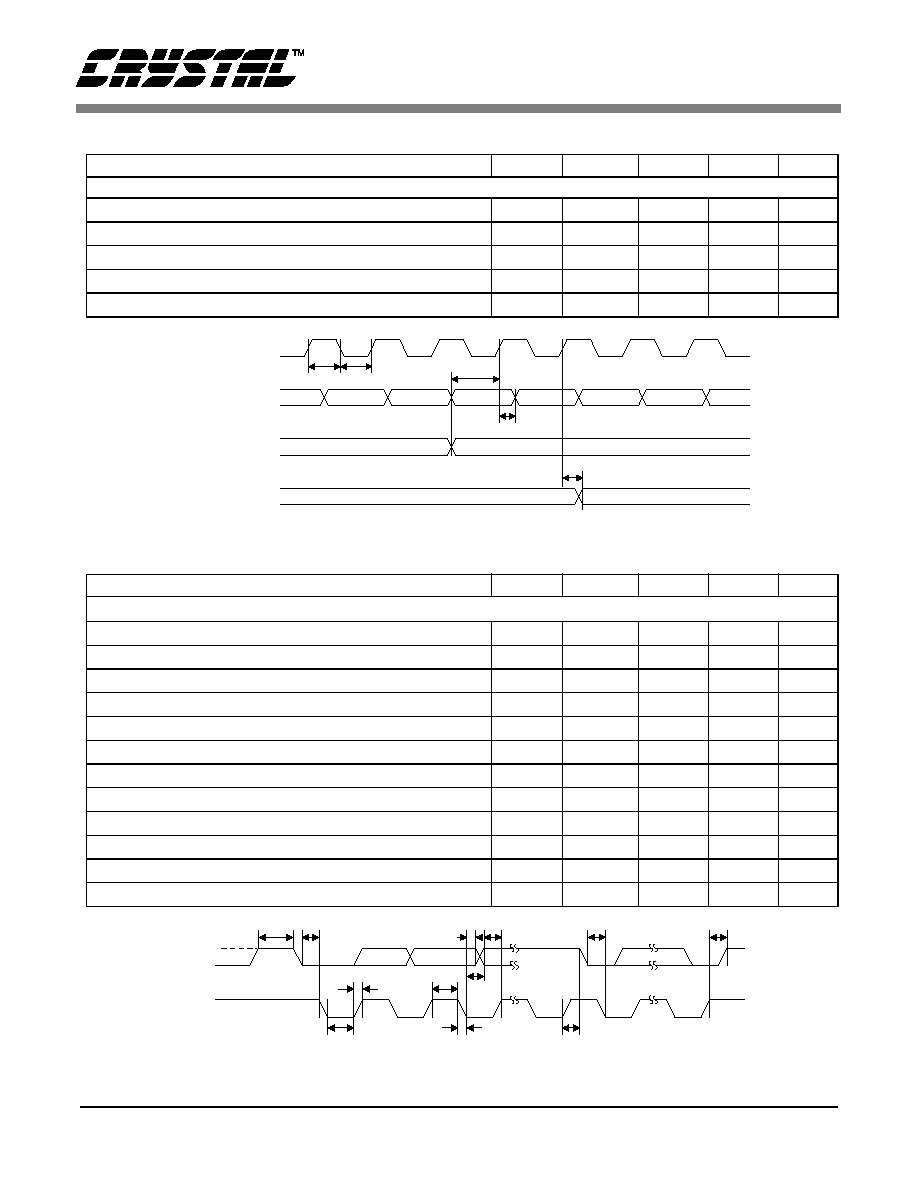
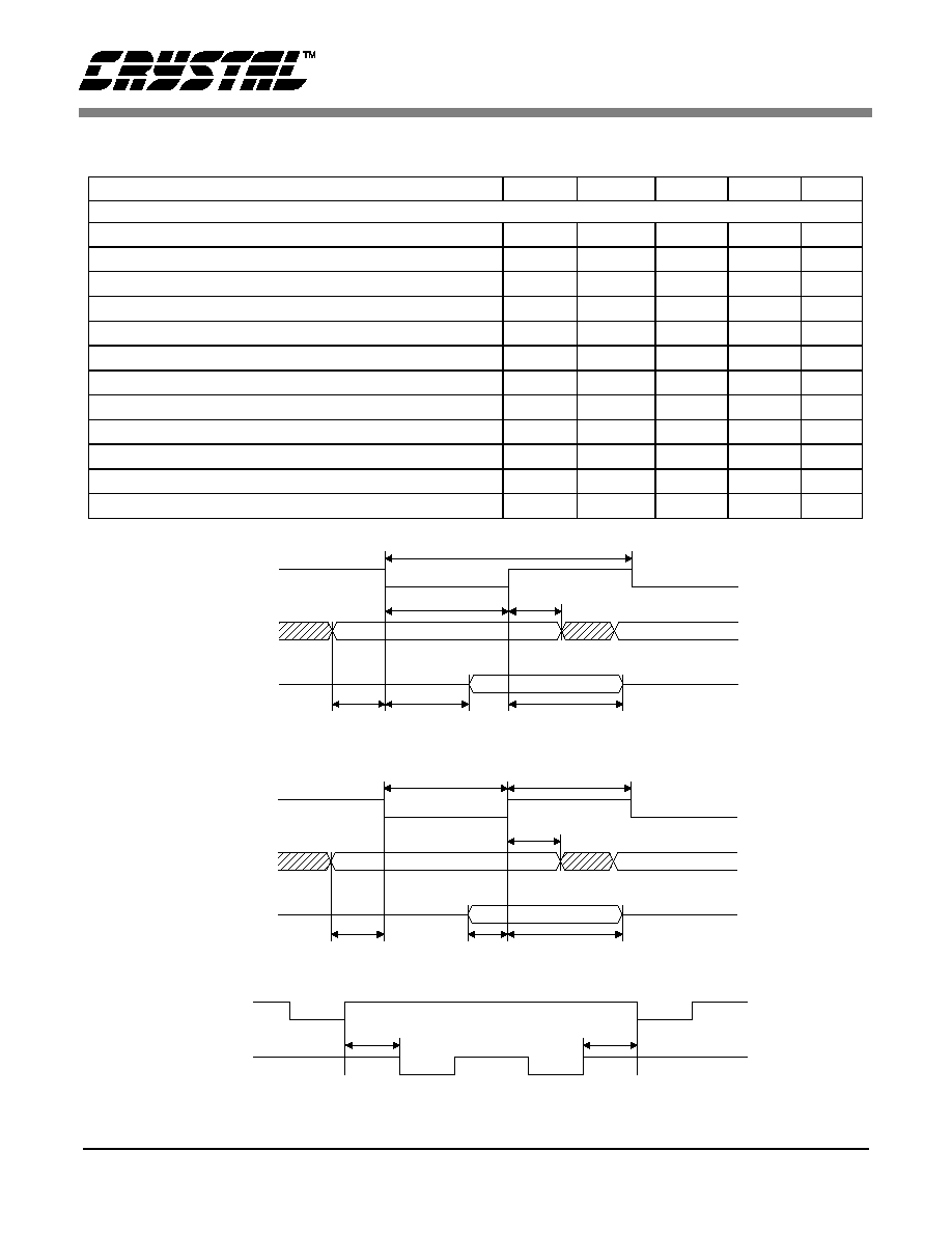
A.C. CHARACTERISTICS:
T
ch
T
cl
T
isu
T
ih
T
oa
CLK
V[7:0]
HSYNC*/VSYNC*
(Inputs)
HSYNC*/VSYNC*/
CB/FIELD/INT
(Outputs)
Figure 1. Video Pixel Data and Control Port Timing
Parameter
Symbol
Min
Typ
Max
Units
Pixel Input and Control Port
Clock Pulse High Time
T
ch
14.82
18.52
22.58
ns
Clock Pulse Low Time
T
cl
14.82
18.52
22.58
ns
Clock to Data Set-up Time
T
isu
6
-
-
ns
Clock to Data Hold Time
T
ih
0
-
-
ns
Clock to Data Output Delay
T
oa
-
-
17
ns
Parameter
Symbol
Min
Typ
Max
Units
I
2
C Host Port Timing
SCL Frequency
F
clk
100
1000
KHz
Clock Pulse High Time
T
sph
0.1
µs
Clock Pulse Low Time
T
spl
0.7
µs
Hold Time (Start Condition)
T
sh
100
ns
Setup Time (Start Condition)
T
ssu
100
ns
Data Setup Time
T
sds
50
ns
Rise Time
T
sr
1
µs
Fall Time
T
sf
0.3
µs
Setup Time (Stop Condition)
T
ss
100
ns
Bus Free Time
T
buf
100
ns
Data Hold Time
T
dh
0
ns
SCL Low to Data Out Valid
T
vdo
600
ns
Figure 2. I
2
C Host Port Timing
SDA
SCL
T
sh
T
sr
T
spl
T
sf
T
ssu
T
sph
T
sds
T
sh
T
ss
T
buf
T
vdo
T
dh
CS4952/53
8
DS223PP2
A.C. CHARACTERISTICS:
(Continued)
ADDR
PDAT[7:0]
T
rdh
T
as
T
rpw
T
rda
T
rah
T
rd
RD*
ADDR
PDAT[7:0]
T
as
T
wpw
WR*
T
wds
T
wr
T
wdh
T
wac
RD*
WR*
T
rec
T
rec
Parameter
Symbol
Min
Typ
Max
Units
8-bit Parallel Host Interface
Read Cycle Time
T
rd
60
-
-
ns
Read Pulse Width
T
rpw
30
-
-
ns
Address Setup Time
T
as
3
-
-
ns
Read Address Hold Time
T
rah
10
-
-
ns
Read Data Access Time
T
rda
-
-
40
ns
Read Data Hold Time
T
rdh
10
-
50
ns
Write Recovery Time
T
wr
60
-
-
ns
Write Pulse Width
T
wpw
40
-
-
ns
Write Data Setup Time
T
wds
8
-
-
ns
Write Data Hold Time
T
wdh
3
-
-
ns
Write-Read/Read-Write Recovery Time
T
rec
50
-
-
ns
Address from Write Hold Time
T
wac
0
-
-
ns
8-bit Parallel Host Port Timing: Read Cycle
8-bit Parallel Host Port Timing: Address Write Cycle
8-bit Parallel Host Port Timing: Read-Write/Write-Read Cycle
Figure 3.

CS4952/53
DS223PP2
9
T
res
RESET*
A.C. CHARACTERISTICS:
(Continued)
Parameter
Symbol
Min
Typ
Max
Units
Reset Timing
Reset Pulse Width
T
res
100
ns
Figure 4. Reset Timing

CS4952/53
10
DS223PP2
+5V
(Vcc)
4.7 µF
0.1 µF
L1
Ferrite Bead
XTAL
ADDR
PDAT[7:0]
RD*
WR*
SDA
SCL
CLK
V[7:0]
FIELD
HSYNC*/CB
VSYNC*
TEST
GND
VAA
VREFOUT
VREFIN
CVBS75
CVBS37
Y
C
INT
RESET*
ISET
GPIO Port
18
19
8
31
32
35
36
+5V (Vcc)
1.5k
1.5k
110
110
I C
Controller
2
27 MHz Clock
Pixel Data
8
33
0.1 µF
75
To RF Modulator
75
Composite Video
Connector
75
75
S-Video
Connector
10 k
±
1%
2
21 22 38
CS4952
CS4953
NC
1
3
20 29
7-14
15
16
17
6
40
37
34
44
43
4
5
41
42
Figure 5. Typical Connection Diagram (I
2
C host interface)

CS4952/53
DS223PP2
11
INTRODUCTION
The CS4952/3 is a complete multi-standard digital
video encoder implemented in current 5-volt only
CMOS technology. CCIR601 or CCIR656 compli-
ant digital video input can be converted into
NTSC-M, PAL B, PAL D, PAL G, PAL H, PAL I,
PAL M, PAL N, or PAL N Argentina-compatible
analog video. The CS4952/3 is designed to connect
to MPEG1 and MPEG2 digital video decompres-
sors without glue logic.
Two 9-bit DAC outputs provide high quality
S-Video analog output while two other 9-bit DACs
simultaneously generate composite analog video.
The CS4952/3 will accept 8-bit YCbCr or 8-bit
YUV input data.
The CS4952/3 is completely configured and con-
trolled via an 8-bit host interface port or an I
2
C
compatible serial interface. This host port provides
access and control of all CS4952/3 options and fea-
tures like closed caption insertion, interrupts, etc.
In order to lower the end user set-top overall sys-
tem costs, the CS4952/3 provides an internal volt-
age reference which eliminates the requirement for
an external discrete 3-pin voltage reference.
FUNCTIONAL DESCRIPTION
In the following subsections, the functions of the
CS4952/3 will be described. The descriptions refer
to the block diagram on the cover page.
Video Timing Generator
All timing generation is accomplished via a
27 MHz input applied to the CLK pin. The
CS4952/3 can also accept an optional color burst
crystal on the ADDR & XTAL pins. See section:
Color Subcarrier Synthesizer (page 12), for further
details.
The Video Timing Generator is responsible for or-
chestrating most all of the other modules in the de-
vice. It works in harmony with external sync input
timing or by providing external sync timing out-
puts. It automatically disables color burst on appro-
priate scan lines and generates serration and
equalization pulses on appropriate scan lines.
The CS4952/3 is designed to function as a video
timing master or video timing slave. In both Master
and Slave Modes, all timing is sampled and assert-
ed with the rising edge of the CLK pin.
In most cases the CS4952/3 will serve as the video
timing master. The master timing cannot be exter-
nally altered other than through the host interface
by changing the video display modes: PAL or
NTSC and Progressive Scan. HSYNC, VSYNC
and FIELD are configured as outputs for Master
Mode. HSYNC can also be defined as a composite
blanking output signal in Master Mode. Exact hor-
izontal and vertical display timing is addressed in
section: Operational Description (page 14).
In Slave Mode HSYNC and VSYNC are config-
ured as input pins and are used to initialize inde-
pendent vertical and horizontal timing generators
upon their respective falling edges. FIELD remains
an output in Slave Mode.
The CS4952/3 also provides a CCIR-656 Slave
Mode where the video input stream contains EAV
and SAV codes. In this case, proper HSYNC
VSYNC timing is extracted automatically without
aid from any inputs other than the V [7:0].
CCIR-656 input data is sampled with the leading
edge of CLK. Slave Mode vertical and horizontal
timing derived via CCIR-656 or external hardware
must be equivalent to timing generated by the
CS4952/3 in Master Mode.
Video Input Formatter
The video input formatter translates YCbCr input
data into YUV information, if necessary, and splits
the luma and chroma information for filtering, scal-
ing, and modulation.

CS4952/53
12
DS223PP2
Color Subcarrier Synthesizer
The subcarrier synthesizer is a digital frequency
synthesizer that produces the correct subcarrier fre-
quency for NTSC or PAL. The CS4952/3 generates
the color burst frequency based on the input CLK
(27 MHz). Color burst accuracy and stability are
limited by the accuracy of the 27 MHz input. If the
frequency varies then the color burst frequency will
also vary accordingly.
In order to handle situations in which the CLK var-
ies unacceptably, a local crystal frequency refer-
ence may be used on the ADDR & XTAL device
pins. In this instance the input CLK is continuously
compared with the external crystal reference input
and the internal timing of the CS4952/3 is automati-
cally adjusted so that the color burst frequency re-
mains close to the requirements.
Controls are provided for phase adjustment of the
burst to permit color adjustment and phase com-
pensation. Chroma hue control is provided by the
CS4952/3 via a 10-bit Hue Control Register
(HUE_LSB and H_MSB). Burst amplitude control
is also made available to the host via the 8-bit burst
amplitude register (SC_AMP).
Chroma Path
The Video Input Formatter at conclusion delivers
4:2:2 YUV outputs into separate chroma and luma
data paths. The chroma path will be discussed here.
The chroma output of the Video Input Formatter is
directed to a chroma low pass 19-tap FIR filter. The
filter bandwidth is selected or the filter may be by-
passed via the CONTROL_1 register. The pass-
band of the filter is either 650 KHz or 1.3 MHz and
the passband ripple is less than or equal to 0.05 dB.
The stopband for the 1.3 MHz selection begins at
3 MHz with an attenuation of greater that 35 dB.
The stopband for the 650 KHz selection begins
around 1.1 MHz with an attenuation of greater than
20 dB.
The output of the chroma low pass filter is connect-
ed to the chroma interpolation filter where upsam-
pling from 4:2:2 to 4:4:4 is accomplished. The
chroma digital data is fed to a quadrature modulator
where they are combined with the output from the
subcarrier synthesizer to produce the proper modu-
lated chrominance signal.
Following chroma modulation the chroma data
passes through a variable gain amplifier where the
chroma amplitude may be varied via the C_AMP
8-bit host addressable register. The chroma then is
interpolated by a factor of 2 in order to operate the
output DACs at 2 times the pixel rate. The interpo-
lated filters help reduce the sinx/x roll-off for high-
er frequencies and reduce the complexity of the
external analog low pass filters.
Luma Path
Along with the chroma output path, the CS4952/3
Video Input Formatter initiates a parallel luma data
path by directing the luma data to a digital delay
line. The delay line is built as a digital FIFO where
the depth of the FIFO replicates the clock period
delay associated with the more complex chroma
path.
Following the luma delay, the data is passed
through a variable gain amplifier where the luma
DC values are modifiable via the Y_AMP register.
The output of the luma amplifier connects to the
sync insertion block. Sync insertion is accom-
plished by multiplexing into the luma data path the
different sync DC values at the appropriate times.
The digital sync generator takes horizontal sync
and vertical sync timing signals and generates the
appropriate composite sync timing (including ver-
tical equalization and serration pulses), blanking
information, and burst flag. The sync edge rates
conform to RS-170A or CCIR specifications.
The luma only path is concluded via output interpo-
lation by a factor of two in order to operate the out-
put DACs at two times the pixel rate.

CS4952/53
DS223PP2
13
Digital to Analog Converters
The CS4952/3 provides four complete simulta-
neous 27 MHz DACs for analog video output: one
9-bit for S-video chrominance, one 9-bit for S-Vid-
eo luminance, and two 9-bit composite outputs.
Both S-Video DACs are designed for 37.5
over-
all loads. The two composite 9-bit DACs are not
identical. One DAC is designed to drive 37.5
de-
rived from a double terminated 75
circuit. The
second 9-bit DAC is targeted for an on-board local
video connection where single point 75
termina-
tion is sufficient i.e. Ch3/4 RF modulators, video
amps, muxes.
The DACs can be put into tri-state mode via host
addressable control register bits. Each of the four
DACs has its own separate DAC enable associated
with it. In the disable mode, the 9-bit DACs source
or sink zero current.
For lower power standby scenarios the CS4952/3
also provides power shut-off control for the DACs.
Each DAC has a separate DAC shut-off associated
with it.
Voltage Reference
The CS4952/3 is equipped with an on-board
1.235 V voltage reference generator used by the
Video DACs. For most requirements, the voltage
reference output pin can be connected to the volt-
age reference input pin along with a decoupling ca-
pacitor. Otherwise the voltage reference input may
be connected to an external voltage reference.
Current Reference
The DAC output current per bit is derived in the
current reference block. The current step is speci-
fied by the size of resistor place between the ISET
current reference pin and electrical ground. This
has been optimized for 10k
(see "ISET" on
page 25 for more informmation on selecting the
proper ISET value).
Host Interface
The CS4952/3 provides a parallel 8-bit data inter-
face for overall configuration and control. The host
interface uses active low read and write strobes
along with an active low address enable signal to
provide microprocessor compatible read and write
cycles. Indirect host addressing to the CS4952/3 in-
ternal registers is accomplished via an internal ad-
dress register which is uniquely accessible via bus
write cycles with the host address enable signal as-
serted.
The CS4952/3 also provides an I
2
C compatible se-
rial interface for device configuration and control.
This port can operate in standard or fast (400 KHz)
modes. When in I
2
C mode, the parallel data inter-
face PDAT [7:0] pins may be used as a general pur-
pose I/O port controlled by the I
2
C interface.
Closed Caption Services
The CS4952/3 supports the generation of NTSC
Closed Caption services. Line 21 and Line 284 cap-
tioning can be generated and enabled independent-
ly via a set of control registers. When enabled,
clock run-in, start bit, and data bytes are automati-
cally inserted at the appropriate video lines. A con-
venient interrupt interface simplifies the software
interface between the host processor and the
CS4952/3.
Control Registers
The control and configuration of the CS4952/3 is
primarily accomplished through the control regis-
ter block. All of the control registers are uniquely
addressable via the internal address register. The
control register bits are initialized during a chip re-
set.
See the detailed operation section of this data sheet
for all of the individual register bit allocations, bit
operational descriptions and initialization states.

CS4952/53
14
DS223PP2
OPERATIONAL DESCRIPTION
Reset Hierarchy
The CS4952/3 is equipped with an active low asyn-
chronous reset input pin RESET. RESET is used to
initialize the internal registers and the internal state
machines for subsequent default operation. See the
electrical and timing specification section of this
data sheet for specific CS4952/3 chip reset and
power-on signaling timing requirements and re-
strictions. All chip outputs are valid after a time pe-
riod following RESET pin low.
When the RESET pin is held low, the host interface
in the CS4952/3 is disabled and will not respond to
host initiated bus cycles.
A reset initializes the CS4952/3 internal registers to
their default values as described by Table 5. In the
default state, the CS4952/53 video DACs are dis-
abled and the device is configured to internally pro-
vide blue field video data to the DACs (any input
data present on the V [7:0] pins is ignored). Other-
wise the CS4952/53 registers are configured for
NTSC-M CCIR601 output operation. At a mini-
mum, the DAC register (0x04) must be written (to
enable the DACs) and the IN_MODE bit of the
CONTROL_0 register (0x01) must be set (to en-
able CCIR601 data input on V [7:0]) for the
CS4952/53 to become operational after RESET.
Video Timing
Slave Mode Input Interface
In Slave Mode, the CS4952/3 takes VSYNC and
HSYNC as inputs. Slave Mode is the default fol-
lowing a reset and is changed to Master Mode via a
contol register bit (CONTROL_0 [4]). The
CS4952/3 is limited to CCIR601 horizontal and
vertical input timing. All clocking in the CS4952/3
is generated from the CLK pin. In Slave Mode the
Sync Generator uses externally provided horizontal
and vertical sync signals to synchronize the internal
timing of the CS4952/3.
Video data that is sent to the CS4952/3 must be
synchronized to the horizontal and vertical sync
signals. Figure 6 illustrates horizontal timing for
CCIR601 input in Slave Mode. Note that the
CS4952/3 expects to receive the first active pixel
data on clock cycle 245 (NTSC) when bit
SYNC_DLY=0 in the CONTROL_2 Register
(Ox02). When SYNC_DLY=1, it expects the first
active pixel data on clock cycle 246 (NTSC).
Master Mode Input Interface
The CS4952/3 defaults to Slave Mode following
RESET high but may be switched into Master
Mode via the MSTR bit in the CONTROL_0 Reg-
ister (0x00). In Master Mode, the CS4952/3 uses
the VSYNC, HSYNC and FIELD device pins as
CLK
1706
active pixel
#720
HSYNC* (input)
V[7:0]
(SYNC_DLY=0)
1705
1704
1703
1728
1
2
3
128
129
264
265
266
267
268
1686
1685
1684
1683
1716
1
2
3
128
129
244
245
246
247
248
Y
Cr
Y
Cb
Y
Cr
Y
horizontal blanking
active pixel
#1
active pixel
#2
∑ ∑ ∑
∑ ∑ ∑
∑ ∑ ∑
∑ ∑ ∑
∑ ∑ ∑
∑ ∑ ∑
∑ ∑ ∑
NTSC 27MHz Clock Count
PAL 27MHz Clock Count
1702
1682
active pixel
#720
V[7:0]
(SYNC_DLY=1)
Y
Cr
Y
Cb
Y
Cr
horizontal blanking
active pixel
#1
active pixel
#2
Cb
active pixel
#719
Figure 6. CCIR601 Input Slave Mode Horizontal Timing

CS4952/53
DS223PP2
15
outputs to schedule the proper external delivery of
digital video into the V [7:0] pins. Figure 7 illus-
trates horizontal timing for CCIR601 input in Mas-
ter Mode. Note that the CS4952/3 expects to
receive the first active pixel data on clock cycle 245
(NTSC) when bit SYNC_DLY=0 in the
CONTROL_2 Register (0x02). When
SYNC_DLY=1, it expects the first active pixel data
on clock cycle 246 (NTSC).
Vertical Timing
The CS4952/3 can be selected through the
CONTROL_0 register (0x00) to operate in four
different timing modes: PAL which is 625 vertical
lines 25 frames per second interlaced, NTSC which
is 525 vertical lines 30 frames per second interlaced
and both PAL and NTSC again but in Progressive
Scan where the display is non-interlaced.
The CS4952/3 conforms to standard digital decom-
pression dimensions and does not process digital
input data for the active analog video half lines as
they are typically in the over/underscan region of
televisions. For NTSC, 240 active lines total per
field are processed and for PAL 288 active lines to-
tal per field. Frame vertical dimensions are 480
lines for NTSC and 576 lines for PAL. Table 1
specifies active line numbers for both NTSC and
PAL. Refer to Figure 8 for HSYNC, VSYNC and
FIELD signal timing.
Table 1. Vertical Timing
Horizontal Timing
HSYNC is used to synchronize the horizontal input
to output timing in order to provide proper horizon-
tal alignment. HSYNC defaults to an input pin fol-
lowing RESET but switches to output in Master
Mode (CONTROL_0 [4] = 1). Horizontal timing is
referenced to HSYNC transitioning low. For active
video lines, digital video input is to be applied to
the V [7:0] inputs 244 (NTSC) or 264 (PAL), CLK
periods following HSYNC going low to determine
the horizontal alignment of the active video.
CLK
1706
active pixel
#720
HSYNC* (output)
V[7:0]
(SYNC_DLY=0)
1705
1704
1703
1728
1
2
3
128
129
264
265
266
267
268
1686
1685
1684
1683
1716
1
2
3
128
129
244
245
246
247
248
Y
Cr
Y
Cb
Y
Cr
Y
horizontal blanking
active pixel
#1
active pixel
#2
∑ ∑ ∑
∑ ∑ ∑
∑ ∑ ∑
∑ ∑ ∑
∑ ∑ ∑
∑ ∑ ∑
∑ ∑ ∑
NTSC 27MHz Clock Count
PAL 27MHz Clock Count
CB* (output)
1702
1682
active pixel
#720
V[7:0]
(SYNC_DLY=1)
Y
Cr
Y
Cb
Y
Cr
horizontal blanking
active pixel
#1
active pixel
#2
active pixel
#719
Cb
Figure 7. CCIR601 Input Master Mode Horizontal Timing
MODE
FIELD
ACTIVE
LINES
NTSC
1, 3
2, 4
22-261
285-524
PAL
1, 3, 5, 7
2, 4, 6, 8
23-310
336-623
NTSC Progressive-Scan
NA
22-261
PAL Progressive-Scan
NA
23-310
CS4952/53
16
DS223PP2
NTSC Vertical Timing (odd field)
Line
HSYNC*
VSYNC*
FIELD
3
4
5
6
7
8
9
10
NTSC Vertical Timing (even field)
Line
HSYNC*
VSYNC*
FIELD
PAL Vertical Timing (odd field)
Line
HSYNC*
VSYNC*
FIELD
PAL Vertical Timing (even field)
Line
HSYNC*
VSYNC*
FIELD
264
265
266
267
268
269
270
271
265
1
2
3
4
5
6
7
311
312
313
314
315
316
317
318
Figure 8. Vertical Timing

CS4952/53
DS223PP2
17
NTSC Interlaced
The CS4952/3 supports NTSC-M and PAL-M
modes where there are 525 total lines per frame and
two fixed 262.5 line fields per frame and 30 total
frames occuring per second. Please reference Fig-
ure 9 for NTSC interlaced vertical timing. Each
field consists of 1 line for closed caption, 240 ac-
tive lines of video plus 21.5 lines of blanking.
VSYNC field one transistions low at the beginning
of line 4 and will remain low for 3 lines or (858 x 3)
2574 pixel cycles. The CS4952/3 exclusively re-
serves line 21 of field one for closed caption inser-
tion. Digital video input is expected to be delivered
to the CS4952/3 V [7:0] pins for 240 lines begin-
ning on active video lines 22 and continuing
through line 261. VSYNC field two transistions
low in the middle of line 266 and stays low for 3
lines times and transitions high in the middle of line
269. The CS4952/3 exclusively reserves line 284 of
field two for closed caption insertion. Video input
on the V [7:0] pins is expected between lines 285
through line 525.
PAL Interlaced
The CS4952/3 supports PAL modes B, D, G, H, I,
N, and Combination N where there are 625 total
lines per frame and two fixed 312.5 line fields per
frame and 25 total frames occuring per second.
Please reference Figure 10 for PAL interlaced ver-
tical timing. Each field consists of 288 active lines
of video plus 24.5 lines of blanking.
Figure 9. NTSC Video Interlaced Timming
523
524
525
1
2
3
4
5
6
7
8
9
VSYNC* Drops
10
22
Analog
Field 1
261
262
263
Analog
Field 2
285
284
272
271
270
269
268
267
266
265
264
523
524
525
1
2
3
4
5
6
7
8
9
VSYNC* Drops
10
22
Analog
Field 3
261
262
263
Analog
Field 4
285
284
272
271
270
269
268
267
266
265
264
Burst begins with positive half-cycle
Burst begins with negative half-cycle

CS4952/53
18
DS223PP2
621
622
623
Analog
Field 1
Burst Phase = 135 degrees relative to U
Burst Phase = 225 degrees relative to U
620
624
625
1
2
3
4
5
6
7
23
24
309
310
Analog
Field 2
308
311
312
313
314
315
316
317
318
319
320
336
337
621
622
623
Analog
Field 3
620
624
625
1
2
3
4
5
6
7
23
24
309
310
Analog
Field 4
308
311
312
313
314
315
316
317
318
319
320
336
337
621
622
623
Analog
Field 5
620
624
625
1
2
3
4
5
6
7
23
24
309
310
Analog
Field 6
308
311
312
313
314
315
316
317
318
319
320
336
337
621
622
623
Analog
Field 7
620
624
625
1
2
3
4
5
6
7
23
24
309
310
Analog
Field 8
308
311
312
313
314
315
316
317
318
319
320
336
337
VSYNC* Drops
Figure 10. PAL Video Interlaced Timing

CS4952/53
DS223PP2
19
VSYNC will transition low to begin field one and
will remain low for 2.5 lines or (864 x 2.5) 2160
pixel cycles. Digital video input is expected to be
delivered to the CS4952/3 V [7:0] pins for 287
lines beginning on active video line 24 and continu-
ing through line 310.
Field two begins with VSYNC transitioning low
after 312.5 lines from the beginning of field one.
VSYNC stays low for 2.5 lines times and transi-
tions high with the beginning of line 315. Video in-
put on the V [7:0] pins is expected between line 336
through line 622.
Progressive Scan
The CS4952/3 supports a progessive scan mode
where the video output is non-interlaced. This is
accomplished by displaying only the first video
field for NTSC or PAL. To preserve exact MPEG-2
frame rates of 30 and 25 per second, the CS4952/3
displays the same first field repetitively but alter-
nately varies the field times. Other digital video en-
coders commonly support progressive scan by
repetitively displaying a 262 line field (524/525
lines for NTSC). In the long run this method is
flawed in that over time, the output display rate will
overrun a system clock locked MPEG-2 decom-
pressor and display a field twice every 8.75 sec-
onds.
PAL Progressive Scan
VSYNC will transistion low to begin field one and
will remain low for for 2.5 lines or (864 x 2.5) 2160
pixel times. Please reference Figure 11 for PAL
non-interlaced timing. Digital video input is ex-
pected to be delivered to the CS4952/3 V [7:0] pins
for 288 lines beginning on active video line 23 and
continuing through line 309.
Field two begins with VSYNC transitioning low
after 312 lines from the beginning of field one.
VSYNC stays low for 2.5 line times and transitions
high during the middle of line 315. Video input on
the V [7:0] pins is expected between line 335
through line 622. Field two is 313 lines long while
field one is 312.
NTSC Progressive Scan
VSYNC will transition low at line 4 to begin field
one and will remain low for 3 lines or (858 x 3)
2574 pixel times. Please reference Figure 12 for
NTSC interlaced timing. Digital video input is ex-
pected to be delivered to the CS4952/3 V [7:0] pins
for 240 lines beginning on active video line 22 and
continuing through line 261.
Field two begins with VSYNC transitioning low at
line 266. VSYNC stays low for 2.5 line times and
transitions high during the middle of line 268. Vid-
eo input on the V [7:0] pins is expected between
line 284 through line 524. Field two is 263 lines
long while field one is 262.
CCIR-656
The CS4952/3 supports an additional Slave Mode
feature that is selectable through the CCIR601 bit
of the CONTROL_0 register. The CCIR-656 slave
feature is unique because the horizontal and verti-
cal timing and digital video are combined into a
single 8-bit 27 MHz input. With CCIR-656 there
are no horizontal and vertical input or output
strobes, only 8-bit 27 MHz active CbYCrY data
with start and end of video codes being implement-
ed with reserved 00 and FF code sequences within
the video feed. As with all modes, V [7:0] are sam-
pled with the rising edge of CLK. The CS4952/3
expects the digital CCIR-656 stream to be error
free. The FIELD output toggles as with non
CCIR-656 input. CCIR-656 input timing is illus-
trated in Figure 13.

CS4952/53
20
DS223PP2
309
310
311
Analog
Field 1
Burst Phase = 135 degrees relative to U
Burst Phase = 225 degrees relative to U
312
313
1
2
3
4
5
6
7
23
24
309
Analog
Field 2
308
311
312
VSYNC* Drops
1
2
3
4
5
6
7
23
24
310
309
310
311
Analog
Field 3
312
313
1
2
3
4
5
6
7
23
24
309
Analog
Field 4
308
311
312
1
2
3
4
5
6
7
23
24
310
Figure 11. PAL Video Non-Interlaced Progressive Scan Timing

CS4952/53
DS223PP2
21
261
262
1
2
3
4
5
6
7
8
9
Start of
VSYNC
10
22
Field 1
Burst begins with positive half-cycle
Burst begins with negative half-cycle
Burst phase = reference phase = 180 relative to B-Y
0
Burst phase = reference phase = 180 relative to B-Y
0
262
263
1
2
3
4
5
6
7
8
9
10
22
261
262
1
2
3
4
5
6
7
8
9
10
22
262
263
1
2
3
4
5
6
7
8
9
10
22
Field 2
Field 3
Field 4
Start of
VSYNC
Figure 12. NTSC Video Non-Interlaced Progressive Scan Timing
Composite
Video
V[7:0]
Active Video
Y Cr Y FF
10
XY
00
EAV Code
4 Clocks
00
80 10 80 10
80 10 80
80 10
80 10 80 10 FF
XY
00 00
Cb Y Cr Cb Y Cr
Ancilliary Data
268 Clocks (NTSC)
280 Clocks (PAL)
Horizontal Blanking
SAV Code
4 Clocks
Active Video
1440 Clocks
CCIR656
DATA
Figure 13. CCIR656 Input Mode Timing
CS4952/53
22
DS223PP2
Digital Video Input Modes
The CS4952/3 provides 2 different digital video in-
put modes that are selectable through the
IN_MODE bit of the CONTROL_0 register.
In mode 0 and upon RESET, the CS4952/3 defaults
to output a solid color (1 of a possible of 256 col-
ors). The background color is selected by writing
the BKG_COLOR register (0x08). The colorspace
of the register is RGB 3:3:2 and is unaffected by
gamma correction. The default color following RE-
SET is blue.
In mode 1 the CS4952/3 supports a single 8-bit
27 MHz CbYCrY source as input on the V [7:0]
pins. Input video timing can be CCIR601 master or
slave and progressive scan.
Multi-standard Output Format Modes
The CS4952/53 supports a wide range of output
formats compatible with worldwide broadcast stan-
dards. These formats include NTSC-M,
PAL-B/D/G/H/I, PAL-M, PAL-N and PAL Combi-
nation N (PAL-Nc) which is the broadcast standard
used in Argentina. After RESET, the CS4952/53 de-
faults to NTSC-M operation with CCIR601 analog
timing. NTSC-M can also be supported in the Japa-
nese format by turning off the 7.5 IRE pedestal
through the PED bit in the CONTROL_1 register
(0x01).
Output formats are configured by writing control
registers as shown in Table 2.
Subcarrier Generation
The CS4952/3 automatically synthesizes NTSC
and PAL color subcarrier clocks using the CLK fre-
quency and four control registers
(SC_SYNTH0/1/2/3). The NTSC subcarrier syn-
thesizer is reset every four fields and every eight
fields for PAL.
The SC_SYNTH0/1/2/3 registers used together
provide a 32-bit value which defaults to NTSC val-
ues of 43E0F83Eh following reset.
Table 3 indicates the 32-bit value required for the
different broadcast formats.
Subcarrier Compensation
Since the subcarrier is synthesized from CLK the
subcarrier frequency error will track the clock fre-
quency error. If the input clock has a tolerance of
200 ppm then the resulting subcarrier will also
have a tolerance of 200 ppm. Per the NTSC speci-
fication the final subcarrier tolerance is ±10 Hz
which is more like 3 ppm. Care must be taken in se-
lecting a suitable clock source.
In MPEG-2 system environments the clock is actu-
ally recovered from the data stream. In these cases
the recovered clock can be 27 MHz ±50 ppm or
Address
Register
NTSC-MC
CIR601
NTSC-MCCI
R60
(Japan)
NTSC-MR
S170A
PAL-B,D,
G,H,I
PAL-M
PAL-N
PAL-NCom
(Argentina)
0x00
CONTROL_0
01h
01h
21h
41h
61h
A1h
81h
0x01
CONTROL_1
04h
00h
04h
04h
04h
04h
04h
0x10
SC_AMP
1Ch
1Ch
1Ch
15h
15h
15h
15h
0x11
SC_SYNTH0
3Eh
3Eh
3Eh
96h
4Eh
96h
8Ch
0x12
SC_SYNTH1
F8h
F8h
F8h
15h
4Ah
15h
28h
0x13
SC_SYNTH2
E0h
E0h
E0h
13h
E1h
13h
EDh
0x14
SC_SYNTH3
43h
43h
43h
54h
43h
54h
43h
Table 2. Multi-standard Format Register Configurations
(Slave Mode, interlaced timing, non-656 data)

CS4952/53
DS223PP2
23
±1350 Hz. It varies per television but in many cases
given an MPEG-2 system clock of 27 MHz
±1350 Hz the resultant color subcarrier produced
will be outside of the televisions ability to compen-
sate and the chrominance information will not be
displayed (black and white picture only).
The CS4952/3 is designed to provide automatic
compensation for an excessively inaccurate
MPEG-2 system clock. Sub-carrier compensation
is enabled through the XTAL bit of the
CONTROL_2 register. When enabled the
CS4952/3 will utilize a common quartz color burst
crystal (3.579545 MHz ±50 ppm for NTSC) at-
tached to the ADDR and XTAL pins to automati-
cally compare and compensate the color subcarrier
synthesis process. Use of the ADDR and XTAL
pins requires that the host interface is configured
for I
2
C operation.
Closed Caption Insertion
The CS4952/3 is capable of NTSC Closed Caption
insertion on lines 21 and 284 independently.
Closed captioning is enabled for either or both lines
21 & 284 via the CC_EN [1:0] register bits and data
to be inserted is also written into the four Closed
Caption Data registers. The CS4952/3 when en-
abled automatically generates the seven cycles of
clock run-in (32 x line rate), start bit insertion
(001)and finally insertion of the two data bytes per
line. Data low at the video outputs corresponds to 0
IRE and data high corresponds to 50 IRE.
There are two independent 8-bit registers per line
(CC_21_1 & CC_21_2 for line 21 and CC_284_1
& CC_284_2 for line 284). Interrupts are also pro-
vided to simplify the handshake between the driver
software and the chip. Typically the host would
write all 4 bytes to be inserted into the registers and
then enable closed caption insertion and interrupts.
As the closed caption interrupts occur the host soft-
ware would respond by writing the next two bytes
to be inserted to the correct control registers and
then clear the interrupt and wait for the next field.
Color Bar Generator
The CS4952/3 is equipped with a color bar genera-
tor that is enabled through the CBAR bit of the
CONTROL_1 register. The color bar generator
works in Master or Slave Mode and has no effect
on the video input/output timing. If the CS4952/3 is
configured for Slave Mode color bars, proper video
timing must be present on the HSYNC and
VSYNC pins for the color bars to be displayed.
Given proper Slave Mode input timing or Master
Mode, the color bar generator will override the vid-
eo input pixel data.
The output of the color bar generator is instantiated
after the chroma interpolation filter and before the
luma delay line. The generated color bar numbers
are for 100% amplitude, 100% saturation NTSC
EIA color bars or 100% amplitude, 100% satura-
tion PAL EBU color bars. For PAL color bars, the
CS4952/3 generates NTSC color bar values, which
are very close to standard PAL values. The exact
luma and chroma values are listed in Table 4.
System
Fsubcarrier
Value (dec)
Value (hex)
NTSC-M
3.5795455 MHz
1138817086
43E0F83E
PAL-B, D, G, H, I, N
4.43361875 MHz
1410536854
54131596
PAL-N (Argentina)
3.582056 MHz
1139615885
43ED288D
PAL-M
3.579611 MHz
1138838095
43CDDFC7
Table 3. Multi-standard Format FSC Register Configurations

CS4952/53
24
DS223PP2
Table 4. Internal Color Bar Values
(8-bit values, Cb/Cr are in 2's complement format)
Interrupts
In order to better support precise video mode
switches and to establish a software/hardware
handshake with the closed caption insertion block
the CS4952/3 is equipped with an interrupt pin
named INT. The INT pin is active high. There are
three interrupt sources: VSYNC, Line 21 and Line
284. Each interrupt can be individually disabled
with the INT_EN register. Each interrupt is also
cleared via writing a one to the corresponding
INT_CLR register bits. The three individual inter-
rupts are ORed together to generate an interrupt
signal which is presented on the INT output pin. If
an interrupt has occurred, it cannot be eliminated
with a disable, it must be cleared.
General Purpose I/O Port
The CS4952/53 has a GPIO port and register which
is available when the device is configured for I
2
C
host interface operation. In I
2
C host interface
mode, the PDAT [7:0] pins are unused by the host
interface and they may operate independently as in-
put or output pins for the GPIO_DATA_REG reg-
ister (0x0A). The CS4952/53 also contains the
GPIO_CTRL_REG Register (0x09) which is used
to configure the GPIO pins for input or output op-
eration.
The GPIO port PDAT [7:0] pins are configured for
input operation when the corresponding
GPIO_CTRL_REG [7:0] bits are cleared. In GPIO
input mode, the CS4952/53 will latch the data on
the PDAT [7:0] pins into the corresponding bit lo-
cations of GPIO_DATA_REG when it detects reg-
ister address 0x0A through the I
2
C interface. A
detection of address 0x0A can happen in two ways.
The first and most common way this will happen is
when address 0x0A is written to the CS4952/53 via
its I
2
C interface. The second method for detecting
address 0x0A is implemented by accessing register
address 0x09 through I
2
C. In I
2
C host interface op-
eration, the CS4952/53 register address pointer will
auto-increment to address 0x0A after an address
0x09 access.
The GPIO port PDAT [7:0] pins are configured for
output operation when the corresponding
GPIO_CTRL_REG [7:0] bits are set. In GPIO out-
put mode, the CS4952/53 will output the data in
GPIO_DATA_REG [7:0] bit locations onto the
corresponding PDAT [7:0] pins when it detects a
register address 0x0A through the I
2
C interface.
ANALOG
Analog Timing
All CS4952/3 analog timing and sequencing is de-
rived from the 27 MHz clock input. The analog out-
puts are controlled internally by the video timing
generator in conjunction with master and slave tim-
ing. The video output signals perform accordingly
for NTSC, PAL specifications and both modes again
but with progressive scan non-interlaced video out-
put.
Being that the CS4952/3 is almost entirely a digital
circuit, great care has been taken to guarantee ana-
log timing and slew rate performance as specified
in the NTSC and PAL analog specifications. Refer-
ence the Analog Parameters section of this data
sheet for exact performance parameters.
COLOR
Cb
Cr
Y
White
0
0
+180
Yellow
-84
+14
+162
Cyan
+28
-84
+131
Green
-56
-70
+112
Magenta
+56
+70
+84
Red
-28
+84
+69
Blue
+84
-14
+35
Black
0
0
+16

CS4952/53
DS223PP2
25
VREF
The CS4952/3 can operate with or without the aid
of an external voltage reference. The CS4952/3 is
designed with an internal voltage reference genera-
tor that provides a VREFOUT signal. The internal
voltage reference is utilized by electrically con-
necting the VREFOUT and VREFIN pins. VRE-
FIN can also be connected to an external precision
1.235 volt reference. In either case, VREFIN is to
be decoupled to ground with a 0.1
µ
F capacitor.
Decoupling should be applied as close to the device
pin as possible.
ISET
All four of the CS4952/3 digital to analog converter
DACs are output current normalized with a com-
mon ISET device pin. The DAC output current per
bit is determined by the size of the resistor connect-
ed between ISET and electrical ground. Typically a
10 k
±1% metal film resistor should be used. The
ISET resistance can be changed by the user to ac-
commodate varying video output attenuation via
post filters and also to suit individual preferred per-
formance.
In conjunction with the ISET value, the user may
also independently vary the chroma, luma and col-
orburst amplitude levels via host addressable con-
trol register bits that are used to control internal
digital amplifiers. The DAC output levels are de-
fined by the following operations:
VREFIN/RISET = IREF
1.235 V/10 k
= 123.5 µA
CVBS37/Y/C Outputs:
VOUT (max) = IREF
◊
(8/15)
◊
511
◊
37.5
=
1.262 V
CVBS75 Output:
VOUT (max) = IREF
◊
(4/15)
◊
511
◊
75
=
1.262 V
DACs
The CS4952/3 is equipped with 4 independent vid-
eo grade current output digital to analog converters.
They are 9-bit DACs operating at a 27 MHz two
times oversampling rate. All four DACs are dis-
abled and put in a low power mode upon RESET.
All four DACs can be individually powered down
and disabled. The output current per bit of all four
DACs is determined by the size of resistor connect-
ed between the ISET pin and electrical ground.
Luminance DAC
The Y pin is driven from a 9-bit 27 MHz current
output DAC that internally receives the Y or lumi-
nance portion of the video signal (black and white
intensity and syncronization information only). Y
is designed to drive proper video levels into a
37.5
load. Reference the detailed electrical sec-
tion of this data sheet for the exact Y digital to an-
alog AC and DC performance data. A Y_EN
enable control bit in the DAC register (0x08) is
provided to enable or disable the luminance DAC.
For a complete disable and lower power operation
the Luminance DAC can be totally shut down via
the Y_PD control bit in the DAC register (0x08). In
this mode turn-on through the control register will
not be instantaneous.
Chrominance DAC
The C pin is driven from a 9-bit 27 MHz current
output DAC that internally receives the C or
chrominance portion of the video signal (color
only). C is designed to drive proper video levels
into a 37.5
load. Reference the detailed electrical
section of this data sheet for the exact C digital to
analog AC and DC performance data. A C_EN en-
able control register bit in the DAC register (0x08)
is provided to enable or disable the Chrominance
DAC. For a complete disable and lower power op-
eration the Chrominance DAC can be totally shut
down via the C_PD control register bit in the DAC

CS4952/53
26
DS223PP2
register (0x08). In this mode turn-on through the
control register will not be instantaneous.
CVBS75 DAC
The CVBS75 pin is driven from a 9-bit 27 MHz
current output DAC that internally receives a com-
bined luma and chroma signal to provide compos-
ite video output. CVBS75 is designed to drive
proper composite video levels into a 75
load.
Reference the detailed electrical section of this data
sheet for the exact CVBS75 digital to analog AC
and DC performance data. A C_75_EN enable con-
trol register bit in the DAC register (0x08) is provid-
ed to enable or disable the ouput pin. When
disabled, no current flows from the output. For a
complete disable and lower power operation the
CVBS75 DAC can be totally shut down via the
C_75_PD control register bit in the DAC register
(0x08). In this mode turn-on through the control
register will not be instantaneous.
CVBS37 DAC
The CVBS37 pin is driven from a 9-bit 27 MHz
current output DAC that internally receives a com-
bined luma and chroma signal to provide compos-
ite video output. CVBS37 is designed to drive
proper composite video levels into a 37.5
load.
Reference the detailed electrical section of this data
sheet for the exact CVBS37 digital to analog AC
and DC performance data. The C_37_EN DAC en-
able control register bit is in the DAC register
(0x08) provided to enable or disable the ouput pin.
When disabled, no current flow from the output.
For a complete disable and lower power operation
the CVBS37 DAC can be totally shut down via the
C_37_PD control register bit in the DAC register
(0x08). In this mode turn-on through the control
register will not be instantaneous.

CS4952/53
DS223PP2
27
PROGRAMMING
Host Control Interface
The CS4952/3 host control interface can be config-
ured for I
2
C or 8-bit parallel operation. The
CS4952/3 will default to I
2
C operation when the
RD and WR pins are both tied low at power up. The
RD and WR pins are active for 8-bit parallel oper-
ation only.
I
2
C Interface
The CS4952/3 provides an I
2
C interface for access-
ing the internal control and status registers. External
pins are a bidirectional data pin (SDA) and a serial
input clock (SCL). The protocol follows the I
2
C
specifications. A complete data transfer is shown in
Figure 14. Note that this I
2
C interface will work in
Slave Mode only - it is not a bus master.
SDA and SCL are connected via an external
pull-up resistor to a positive supply voltage. When
the bus is free, both lines are high. The output stag-
es of devices connected to the bus must have an
open-drain or open-collector in order to perform
the wired-AND function. Data on the I
2
C bus can
be transferred at a rate of up to 400 kbits/sec in fast
mode. The number of interfaces to the bus is solely
dependent on the limiting bus capacitance of
400 pF. When 8-bit parallel interface operation is
being used, SDA and SCL can be tied directly to
ground.
The I
2
C bus address for the CS4952/3 is program-
mable via register I2C_ADR (0x0F).
8-bit Parallel Interface
The CS4952/3 is equipped with a full 8-bit parallel
microprocessor write and read control port. Along
with the PDAT [7:0] pins the control port interface
is comprised of host read RD and host write WR
active low strobes and host address enable ADDR
which, when low, enables unique address register
accesses. The control port is used to access internal
registers which configure the CS4952/3 for various
modes of operation. The internal registers are
uniquely addressed via an address register. The ad-
dress register is accessed during a host write cycle
with the WR and ADDR pins set low. Host write
cycles with ADDR set high will write the 8-bits on
the PDAT [7:0] pins into the register currently se-
lected by the address register. Likewise read cycles
occur with RD set low and ADDR set high will re-
turn the register contents selected by the address
register. Reference the detailed electrical timing
parameter section of this data sheet for exact host
parallel interface timing characteristics and specifi-
cations. When I
2
C interface operation is being
used, RD and WR must be tied to ground.
PDAT [7:0] are available to be used for GPIO op-
eration in I
2
C host interface mode.
SDA
SCL
I C Protocol
2
Start
Address
R/W
ACK
Data
Stop
A
P
1-7
8
9
ACK
1-7
8
9
Data
ACK
1-7
8
9
Note: I C transfers data always with MSB first, LSB last
2
Figure 14. I
2
C Data Transfer

CS4952/53
28
DS223PP2
Register Description
A set of internal registers are available for control-
ling the operation of the CS4952/3. The registers
extend from internal address 0x00 through 0x3D.
Table 5 shows a complete list of these registers and
their internal addresses. Note that this table and the
subsequent register description section describe the
full register map for CS4952 only. A complete
CS4953 register set description is only available to
Macrovision ACP-PPV Licensed Buyers.
Address
Register Name
Type
Default Value
0x00
CONTROL_0
r/w
01h
0x01
CONTROL_1
r/w
04h
0x02
CONTROL_2
r/w
00h
0x03
RESERVED
0x04
DAC
r/w
F0h
0x05 - 0x06
RESERVED
0x07
STATUS
read only
00h
0x08
BKG_COLOR
r/w
03h
0x09
GPIO_CTRL_REG
r/w
0x0A
GPIO_DATA_REG
r/w
00h
0x0B - 0x0C
RESERVED
0x0D
C_AMP
r/w
80h
0x0E
Y_AMP
r/w
80h
0x0F
I2C_ADR
r/w
n/a
0x10
SC_AMP
r/w
1Ch
0x11
SC_SYNTH0
r/w
3Eh
0x12
SC_SYNTH1
r/w
F8h
0x13
SC_SYNTH2
r/w
E0h
0x14
SC_SYNTH3
r/w
43h
0x15
HUE_LSB
r/w
00h
0x16
HUE_MSB
r/w
00h
0x17
RESERVED
0x18
CC_EN
r/w
00h
0x19
CC_21_1
r/w
00h
0x1A
CC_21_2
r/w
00h
0x1B
CC_284_1
r/w
00h
0x1C
CC_284_2
r/w
00h
0x1D - 0x3A
RESERVED
0x3B
INT_EN
r/w
00h
0x3C
INT_CLR
r/w
00h
0x3D
ID_REG
read only
n/a
Table 5. Control Register Map

CS4952/53
DS223PP2
29
Control Register 0
Address
0x00
CONTROL_0
Read/Write
Default Value = 01h
Control Register 1
Address
0x01
CONTROL_1
Read/Write
Default Value = 04h
Bit Number
7
6
5
4
3
2
1
0
Bit Name
TV_FMT
MSTR
CCIR656
PROG
IN_MODE CBCR_UV
Default
0
0
0
0
0
0
0
1
Bit
Mnemonic
Function
7:5
TV_FMT
selects the TV display format
000:
NTSC-M CCIR601 timing (default)
001:
NTSC-M RS170A timing
010:
PAL-B, D, G, H, I
011:
PAL-M
100:
PAL-N (Argentina)
101:
PAL-N (non Argentina)
110-111:
reserved
4
MSTR
1: Master Mode, 0: Slave Mode
3
CCIR656
video input is in CCIR656 format (0: off, 1: on)
2
PROG
Progressive scanning enable (enable with 1)
1
IN_MODE
Input select (0: solid background, 1: use V [7:0] data)
0
CBCR_UV
enable YCbCr to YUV conversion (1: enable, 0: disable)
Bit Number
7
6
5
4
3
2
1
0
Bit Name
CBLANK
Y_DELAY
C_BW
C_LPF_EN
FLD
PED
CBAR
CBCRSEL
Default
0
0
0
0
0
1
0
0
Bit
Mnemonic
Function
7
CBLANK
Composite Blank / HSYNC output select (1: CB, 0: HSYNC)
6
Y_DELAY
luma to chroma delay (0: no delay, 1: luma is delayed by one 13.5 MHz cycle)
5
C_BW
chroma lpf bandwidth (0: 650 KHz, 1: 1.3 MHz)
4
C_LPF_EN
chroma lpf on/off (0: off, 1: on)
3
FLD
Polarity of Field (0: odd field - 0, 1: odd field - 1)
2
PED
Pedestal offset (0: 0 IRE, 1: 7.5 IRE)
1
CBAR
internal color bar generator (0: off, 1: on)
0
CBCRSEL
CbCr select (0: chroma undelayed, 1: chroma delayed by one clock)

CS4952/53
30
DS223PP2
Control Register 2
Address
0x02
CONTROL_2
Read/Write
Default Value = 00h
DAC Power Down Register
Address
0x04
DAC
Read/Write
Default Value = F0h
Bit Number
7
6
5
4
3
2
1
0
Bit Name
RESERVED
SYNC_DLY
XTAL
SC_EN
Default
0
0
0
0
0
0
0
0
Bit
Mnemonic
Function
7:4
-
reserved
3
Y_BW
Selects between 4.2 Mhz and 6 Mhz on-chip luminance low pass filters; default
value is zero which selects the 4.2 Mhz low pass filter option
2
SYNC_DLY
Delays expected timing of first active pixel input data relative to falling edge of
HSYNC from 245 27 MHz clock cycles to 246 for NTSC and from 265 to 266 for
PAL. Default State is SYNC_DLY=0 for no delay
1
XTAL
Crystal oscillator for subcarrier adjustment enable (1: enable)
0
SC_EN
Chroma burst disable (1: disable)
Bit Number
7
6
5
4
3
2
1
0
Bit Name
C_75_PD
C_37_PD
Y_PD
C_PD
C_75_EN
C_37_EN
Y_EN
C_EN
Default
1
1
1
1
0
0
0
0
Bit
Mnemonic
Function
7
C_75_PD
power down composite DAC with 75
load (0: power up, 1: power down)
6
C_37_PD
power down composite DAC with 37.5
load (0: power up, 1: power down)
5
Y_PD
power down luma s-video DAC (0: power up, 1: power down)
4
C_PD
power down chroma s-video DAC (0: power up, 1: power down)
3
C_75_EN
enable composite video DAC output for 75
(0: tri-state, 1: enable)
2
C_37_EN
enable composite video DAC output for 37.5
(0: tri-state, 1: enable)
1
Y_EN
enable s-video DAC for luma output (0: tri-state, 1: enable)
0
C_EN
enable s-video DAC for chroma output (0: tri-state, 1: enable)
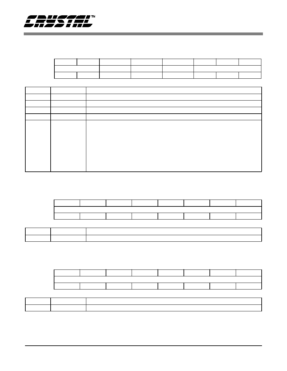
CS4952/53
DS223PP2
31
Status Register
Address
0x07
STATUS
Read Only
Default Value = 00h
Background Color Register
Address
0x08
BKG_COLOR
Read/Write
Default Value = 03h
GPIO Control Register
Address
0x09
GPIO_CTRL_REG
Read/Write
Default Value = 00h
Bit Number
7
6
5
4
3
2
1
0
Bit Name
RESERVED
CC_INT_21
CC_INT_284
VS_INT
FIELD
Default
0
0
0
0
0
0
0
0
Bit
Mnemonic
Function
7:6
-
reserved
5
CC_INT_21
Interrupt flag for line 21 (closed caption) complete
4
CC_INT_284
Interrupt flag for line 284 (closed caption) complete
3
VS_INT
Interrupt flag for video field change
2:0
FIELD
Field Status bits
000: field 8
001: field 1
010: field 2
011: field 3
100: field 4
101: field 5
110: field 6
111: field 7
Bit Number
7
6
5
4
3
2
1
0
Bit Name
BG_COLR
Default
0
0
0
0
0
0
1
1
Bit
Mnemonic
Function
7:0
BG_COLR
Background color (7:5 = R, 4:2 = G, 1:0 = B)
Bit Number
7
6
5
4
3
2
1
0
Bit Name
GPIO_IO
Default
0
0
0
0
0
0
0
0
Bit
Mnemonic
Function
7:0
GPIO_IO
input(0)/output(1) control of GPIO registers (bit X: PDAT(X) I/O configuration)

CS4952/53
32
DS223PP2
GPIO Data Register
Address
0x0A
GPIO_DATA_REG
Read/Write
Default Value = 00h
Chroma Filter Register
Address
0x0D
C_AMP
Read/Write
Default Value = 80h
Luma Filter Register
Address
0x0E
Y_AMP
Read/Write
Default Value = 80h
I
2
C Address Register
Address
0x0F
I2C_ADR
Read/Write
Default Value = N/A
Bit Number
7
6
5
4
3
2
1
0
Bit Name
GPIO_DATA
Default
0
0
0
0
0
0
0
0
Bit
Mnemonic
Function
7:0
GPIO_DATA
GPIO data register; data is output on PDAT [7:0] bus if appropriate bit in
GPIO_CTRL_REG (0x09) is set to "1"; data on PDAT [7:0] is latched into
GPIO_DATA_REG [7:0] when register address 0x0A is accessed via I
2
C.
This register is only accessible in I
2
C mode.
Bit Number
7
6
5
4
3
2
1
0
Bit Name
C_COEF
Default
1
0
0
0
0
0
0
0
Bit
Mnemonic
Function
7:0
C_COEF
Chroma amplitude coefficient
Bit Number
7
6
5
4
3
2
1
0
Bit Name
Y_COEF
Default
1
0
0
0
0
0
0
0
Bit
Mnemonic
Function
7:0
Y_COEF
Luma amplitude coefficient
Bit Number
7
6
5
4
3
2
1
0
Bit Name
RESERVED
ADDR
Default
-
-
-
-
-
-
-
-
Bit
Mnemonic
Function
7
-
reserved
6:0
ADDR
I
2
C device address (programmable)
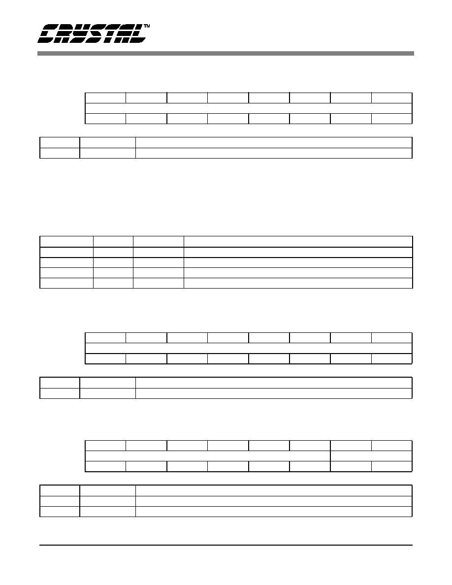
CS4952/53
DS223PP2
33
Subcarrier Amplitude Register
Address
0x10
SC_AMP
Read/Write
Default Value = 1Ch
Subcarrier Synthesis Register
Address
0x11
SC_SYNTH0
Read/Write
Default Value = 3Eh
0x12
SC_SYNTH1
F8h
0x13
SC_SYNTH2
E0h
0x14
SC_SYNTH3
43h
Hue LSB Adjust Register
Address
0x15
HUE_LSB
Read/Write
Default Value = 00h
Hue MSB Adjust Register
Address
0x16
HUE_MSB
Read/Write
Default Value = 00h
Bit Number
7
6
5
4
3
2
1
0
Bit Name
AMP
Default
0
0
0
1
1
1
0
0
Bit
Mnemonic
Function
7:0
AMP
Color burst amplitude
Register
Bits
Mnemonic
Function
SC_SYNTH0
7:0
-
Subcarrier synthesis bits 7:0
SC_SYNTH1
7:0
-
Subcarrier synthesis bits 15:8
SC_SYNTH2
7:0
-
Subcarrier synthesis bits 23:16
SC_SYNTH3
7:0
-
Subcarrier synthesis bits 31:24
Bit Number
7
6
5
4
3
2
1
0
Bit Name
LSB
Default
0
0
0
0
0
0
0
0
Bit
Mnemonic
Function
7:0
LSB
8 LSBs for hue phase shift
Bit Number
7
6
5
4
3
2
1
0
Bit Name
RESERVED
MSB
Default
0
0
0
0
0
0
0
0
Bit
Mnemonic
Function
7:2
-
reserved
1:0
MSB
2 MSBs for hue phase shift
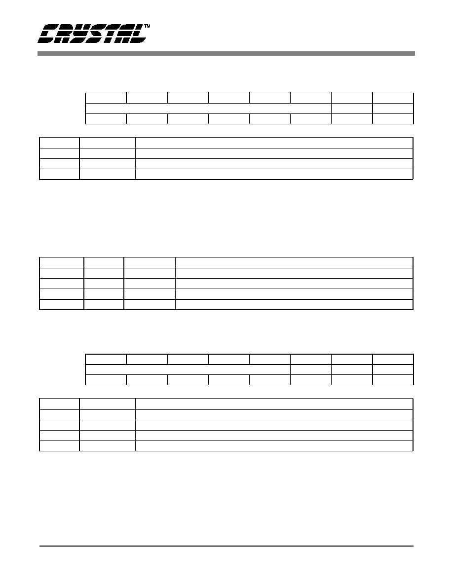
CS4952/53
34
DS223PP2
Closed Caption Enable Register
Address
0x18
CC_EN
Read/Write
Default Value = 00h
Closed Caption Data Register
Address
0x19
CC_21_1
Read/Write
Default Value = 00h
0x1A
CC_21_2
00h
0x1B
CC_284_1
00h
0x1C
CC_284_2
00h
Interrupt Enable Register
Address
0x3B
INT_EN
Read/Write
Default Value = 00h
Bit Number
7
6
5
4
3
2
1
0
Bit Name
RESERVED
EN_284
EN_21
Default
0
0
0
0
0
0
0
0
Bit
Mnemonic
Function
7:2
-
reserved
1
EN_284
enable closed caption for line 284
0
EN_21
enable closed caption for line 21
Register
Bit
Mnemonic
Function
CC_21_1
7:0
-
first closed caption databyte of line 21
CC_21_2
7:0
-
second closed caption databyte of line 21
CC_284_1
7:0
-
first closed caption databyte of line 284
CC_284_2
7:0
-
second closed caption databyte of line 284
Bit Number
7
6
5
4
3
2
1
0
Bit Name
RESERVED
EN_21
EN_284
VS_EN
Default
0
0
0
0
0
0
0
0
Bit
Mnemonic
Function
7:3
-
reserved
2
EN_21
interrupt enable for closed caption line 21
1
EN_284
interrupt enable for closed caption line 284
0
VS_EN
interrupt enable for new field

CS4952/53
DS223PP2
35
Interrupt Clear Register
Address
0x3C
INT_CLR
Read/Write
Default Value = 00h
Device ID Register
Address
0x3D
ID_REG
Read Only
Default Value = N/A
Bit Number
7
6
5
4
3
2
1
0
Bit Name
RESERVED
CLR_21
CLR_284
VS_CLR
Default
0
0
0
0
0
0
0
0
Bit
Mnemonic
Function
7:3
-
reserved
2
CLR_21
clear interrupt for closed caption line 21 (INT_21)
1
CLR_284
clear interrupt for closed caption line 284 (INT_284)
0
VS_CLR
clear interrupt for new video field (INT_V)
Bit Number
7
6
5
4
3
2
1
0
Bit Name
DEV_ID
RESERVED
Default
0
0
0
0
-
-
-
-
Bit
Mnemonic
Function
7:4
DEV_ID
0000 device ID for CS4952
0001 device ID for CS4953
3:0
-
These bits are reserved and the value they return on a read is not defined

CS4952/53
36
DS223PP2
BOARD DESIGN & LAYOUT
CONSIDERATIONS
The printed circuit layout should be optimized for
lowest noise on the CS4952/3 power and ground
lines. Digital and analog sections should be physi-
cally separated and the CS4952/3 placed as close to
the output connectors as possible. All analog sup-
ply traces should be as short as possible to mini-
mize inductive ringing.
A well designed power distribution network is es-
sential in eliminating digital switching noise. The
ground planes must provide a low-impedance re-
turn path for the digital circuits. A PC board with a
minimum of four layers is recommended. The
ground layer should be used as a shield to isolate
noise from the analog traces. The top layer (1)
should be reserved for analog traces but digital
traces may share this layer if the digital signals
have low edge rates and switch little current or if
they are separated from the analog traces by a sig-
nificant distance (dependent on their frequency
content and current). The second layer should then
be the ground plane followed by the analog power
plane on layer three and the digital signal layer on
layer four
Power and Ground Planes
The power and ground planes need isolation gaps
of at 0.05" to minimize digital switching noise ef-
fects on the analog signals and components. A split
analog/digital ground plane should be connected at
one point as close as possible to the CS4952/3. A
split analog/digital power plane should be connect-
ed at one point as close as possible to the power en-
try point and decoupled properly.
Power Supply Decoupling
Start by reducing power supply ripple and wiring
harness inductance by placing a large (33 - 100uF)
capacitor as close to the power entry point as pos-
sible. Use separate power planes or traces for the
digital and analog sections even if they use the
same supply. If necessary, further isolate the digital
and analog power supplies by using ferrite beads on
each supply branch followed by a low ESR capac-
itor.
Place all decoupling caps as close as possible to the
device as possible. Surface mount capacitors gen-
erally have lower inductance than radial lead or ax-
ial lead components. Surface mount caps should be
placed on the component side of the PCB to mini-
mize inductance caused by board vias. Any vias,
especially to ground, should be as large as practical
to reduce their inductive effects.
VREF Decoupling
The VREFOUT pin provides a 1.235 V reference
for the internal DACs. VREFOUT is only intended
to drive VREFIN. Do not connect to an external
load. A small bypass cap, however, may be placed
on VREFOUT to reduce noise. Usually a 0.1uF
MLC surface mount capacitor is sufficient.
Digital Interconnect
The digital inputs and outputs of the CS4952/3
should be isolated from the analog outputs as much
as possible. Use separate signal layers whenever
possible and do not route digital signals over the
analog power and ground planes.
Noise from the digital section is directly related to
the digital edge rates used. Ringing, overshoot, un-
dershoot, and ground bounce are all related to edge
rate. Use lower speed logic such as HCMOS for the
host port interface to reduce switching noise. For
the video input ports, higher speed logic is re-
quired, but use the slowest practical edge rate to re-
duce noise.
To reduce digital noise, it is important to match the
source impedance, line impedance, and load im-
pedance as much as possible. Generally, if the line
length is greater than one fourth the signal edge
rate, line termination is necessary. Ringing may
also be reduced by damping the line with a series
resistor (22 - 150
). Under extreme cases, it may

CS4952/53
DS223PP2
37
be advisable to use microstrip techniques to further
reduce radiated switching noise if very fast edge
rates (<2ns) are used. If microstrip techniques are
used, split the analog and digital ground planes and
use proper RF decoupling techniques.
Analog Interconnect
The CS4952/3 should be located as close as possible
to the output connectors to minimize noise pickup
and reflections due to impedance mismatch. All un-
used analog outputs should be placed in shutdown.
This reduces the total power that the CS4952/3 re-
quires, and eliminates the impedance mismatch pre-
sented by an unused connector. The analog outputs
should not overlay the analog power plane to maxi-
mize high frequency power supply rejection.
Analog Output Protection
To minimize the possibility of damage to the ana-
log out put sections, make sure that all video con-
nectors are well grounded. The connector ground
should have a good DC ground path to the analog
and digital power supply grounds. If no DC (and
low frequency) path is present, improperly ground-
ed equipment may impose damaging reverse cur-
rents on the video out lines. Therefore, it is also a
good idea to use output filters that are AC coupled
to avoid any problems.
ESD Protection
External DAC Output Filter
If an output filter is required for the composite
and/or S-video outputs of the CS4952/53, the fol-
lowing low pass filter in Figure 15 can be used.
2.2
µ
H
330pF
220pF
OUT
IN
C
1
C
2
C
CABLE
C
2
C
1
C
CABLE
should be chosen so that
=
C
2
+
Figure 15. Low Pass Filter

CS4952/53
38
DS223PP2
CS4952/3-CL
44-pin
PLCC
Top View
18
20
22
24
26
28
1
2
4
6
40
42
44
12
8
10
14
16
7
9
11
13
15
17
29
31
33
35
37
39
34
30
32
36
38
VAA
GND
VAA
CVBS37
CVBS75
TEST
V0
V1
V2
V3
V4
V5
V6
V7
FIELD
HSYNC/CB
VSYNC
XTAL
ADDR
VAA
GND
GND
C
Y
VREFOUT
VREFIN
ISET
VAA
GND
RESET
SCL
SDA
INT
CLKIN
WR
RD
PDAT0
PDAT1
PDAT2
PDAT3
PDAT4
PDAT5
PDAT6
PDAT7
DEVICE PINOUT - 44 PLCC

CS4952/53
DS223PP2
39
PLCC Pin Description
Pin Name
Pin Number
Type
Description
V [7:0]
14, 13, 12, 11, 10, 9, 8, 7
IN
Digital video data inputs
CLK
33
IN
27 MHz input clock
ADDR
19
IN
Address enable line / subcarrier crystal input
XTAL
18
OUT
subcarrier crystal output
HSYNC/CB
16
I/O
Active low horizontal sync, or composite blank signal
VSYNC
17
I/O
Active low vertical sync.
FIELD
15
OUT
Video field ID. Selectable polarity
RD
31
IN
Host parallel port read strobe, active low
WR
32
IN
Host parallel port write strobe, active low
PDAT [7:0]
23,24,25,26,27,28,29,30
I/O
Host parallel port/ general purpose I/O
SDA
35
I/O
I
2
C data
SCL
36
IN
I
2
C clock input
CVBS75
5
CURRENT Composite video output for driving 75
loads
CVBS37
4
CURRENT Composite video output for driving 37.5
loads
Y
43
CURRENT Luminance analog output for driving 37.5
loads
C
44
CURRENT Chrominance analog output for driving 37.5
loads
VREFOUT
42
OUT
Internal voltage reference output
VREFIN
41
IN
External voltage reference input
ISET
40
OUT
DAC current set
INT
34
OUT
Interrupt output, active high
RESET
37
IN
Active low master reset
TEST
6
IN
TEST pin. Ground for normal operation
VAA
1, 3, 20, 39
PS
+5 V supply
GND
2, 22, 21, 38
PS
Ground

CS4952/53
40
DS223PP2
INCHES
MILLIMETERS
DIM
MIN
MAX
MIN
MAX
A
0.165
0.180
4.043
4.572
A1
0.090
0.120
2.205
3.048
B
0.013
0.021
0.319
0.533
D
0.685
0.695
16.783
17.653
D1
0.650
0.656
15.925
16.662
D2
0.590
0.630
14.455
16.002
E
0.685
0.695
16.783
17.653
E1
0.650
0.656
15.925
16.662
E2
0.590
0.630
14.455
16.002
e
0.040
0.060
0.980
1.524
JEDEC # : MS-018
44L PLCC PACKAGE DRAWING
D1
D
E1 E
D2/E2
B
e
A1
A

CS4952/53
DS223PP2
41
VAA
GND
VAA
CVBS37
CVBS75
TEST
V0
V1
V2
V3
V4
V5
V6
V7
FIELD
HSYNC/CB
VSYNC
XTAL
ADDR
VAA
GND
GND
C
Y
VREFOUT
VREFIN
ISET
VAA
GND
RESET
SCL
SDA
INT
CLKIN
WR
RD
PDAT0
PDAT1
PDAT2
PDAT3
PDAT4
PDAT5
PDAT6
PDAT7
CS4952/3-CL
44-pin
TQFP
Top View
12
40
42
44
34
36
38
6
2
4
8
10
1
3
5
7
9
11
28
32
30
26
24
33
31
29
27
25
23
14
16
18
20
22
DEVICE PINOUT - 44 TQFP

CS4952/53
42
DS223PP2
TQFP Pin Description
Pin Name
Pin Number
Type
Description
V [7:0]
8, 7, 6, 5, 4, 3, 2, 1
IN
Digital video data inputs
CLKIN
27
IN
27 MHz input clock
ADDR
13
IN
Address enable line / subcarrier crystal input
XTAL
12
OUT
subcarrier crystal output
HSYNC/CB
10
I/O
Active low horizontal sync, or composite blank signal
VSYNC
11
I/O
Active low vertical sync.
FIELD
9
OUT
Video field ID. Selectable polarity
RD
25
IN
Host parallel port read strobe, active low
WR
26
IN
Host parallel port write strobe, active low
PDAT [7:0]
17,18,19,20,21,22,23,24
I/O
Host parallel port/ general purpose I/O
SDA
29
I/O
I
2
C data
SCL
30
IN
I
2
C clock input
CVBS75
43
CURRENT Composite video output for driving 75
loads
CVBS37
42
CURRENT Composite video output for driving 37.5
loads
Y
37
CURRENT Luminance analog output for driving 37.5
loads
C
38
CURRENT Chrominance analog output for driving 37.5
loads
VREFOUT
36
OUT
Internal voltage reference output
VREFIN
35
IN
External voltage reference input
ISET
34
OUT
DAC current set
INT
28
OUT
Interrupt output, active high
RESET
31
IN
Active low master reset
TEST
44
IN
TEST pin. Ground for normal operation
VAA
14, 33, 39, 41
PS
+5 V supply
GND
15, 16, 32, 40
PS
Ground

CS4952/53
DS223PP2
43
INCHES
MILLIMETERS
DIM
MIN
MAX
MIN
MAX
A
0.000
0.065
0.000
1.600
A1
0.002
0.006
0.050
0.150
B
0.012
0.018
0.300
0.450
D
0.478
0.502
11.700
12.300
D1
0.404
0.412
9.900
10.100
E
0.478
0.502
11.700
12.300
E1
0.404
0.412
9.900
10.100
e
0.029
0.037
0.700
0.900
L
0.018
0.030
0.450
0.750
0.000
7.000
0.000
7.000
JEDEC # : MS-026
44L TQFP PACKAGE DRAWING
E1
E
D1
D
1
e
L
B
A1
A
