Document Outline
- CS5330A CS5331A 8-Pin, Stereo A/D Converter for Digital Audio
- Features
- General Description
- ORDERING INFORMATION:
- CHARACTERISTICS/SPECIFICATIONS
- ANALOG CHARACTERISTICS
- DIGITAL CHARACTERISTICS
- DIGITAL FILTER CHARACTERISTICS
- ABSOLUTE MAXIMUM RATINGS
- RECOMMENDED OPERATING CONDITIONS
- SWITCHING CHARACTERISTICS
- SCLK to SDATA LRCK - MASTER mode (CS5330A)
- SCLK to SDATA LRCK - MASTER mode (CS5331A)
- SCLK to LRCK & SDATA - SLAVE mode (CS5330A)
- SCLK to LRCK & SDATA - SLAVE mode (CS5331A)
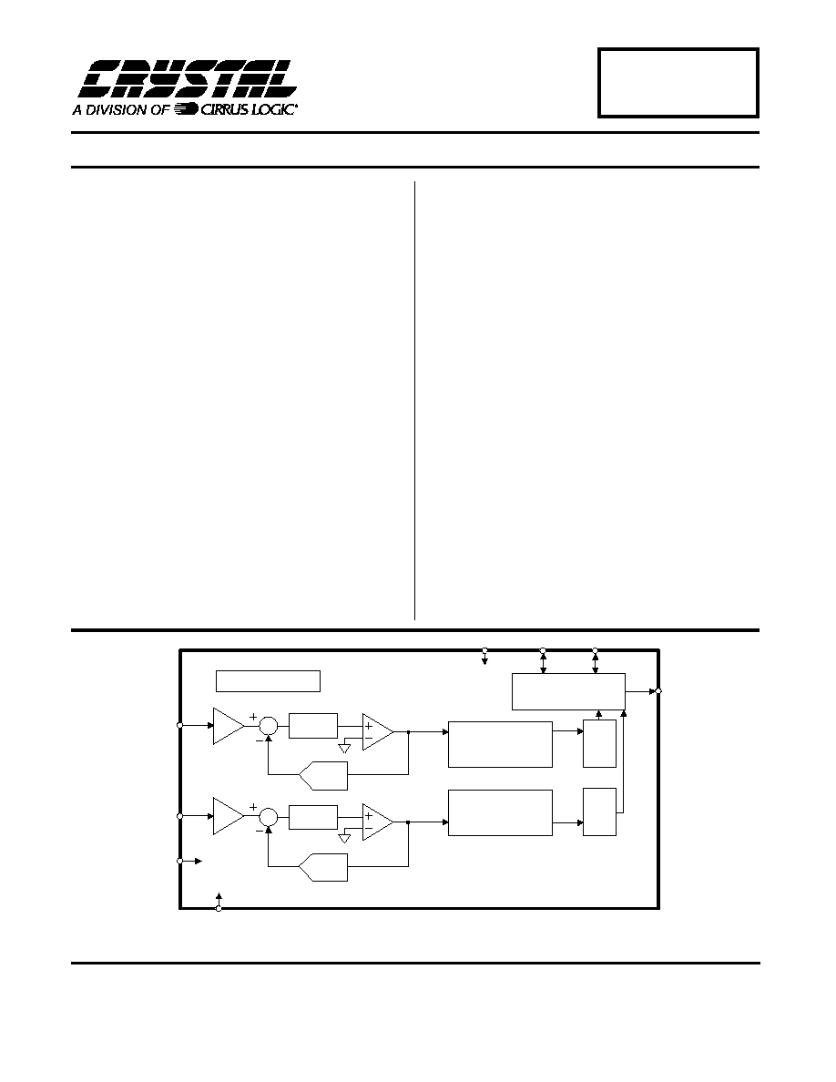
- Figure 1. Typical Connection Diagram
- GENERAL DESCRIPTION
- SYSTEM DESIGN
- Master Clock
- Serial Data Interface
- Table 1. Common Clock Frequencies
- Master Mode
- Slave Mode
- CS5330A
- Figure 2. Data Output Timing - CS5330A
- CS5331A
- Figure 3. Data Output Timing - CS5331A (I 2 S compatible)
- Analog Connections
- High Pass Filter
- Initialization and Power-Down
- Figure 4. CS5330A/31A Initialization and Power-Down Sequence
- Grounding and Power Supply Decoupling
- Digital Filter
- Figure 5. CS5330A/31A Digital Filter Stopband Rejection
- Figure 6. CS5330A/31A Digital Filter Transition Band
- Figure 7. CS5330A/31A Digital Filter Passband Ripple
- Figure 8. CS5330A/31A Digital Filter Transition Band
- PIN DESCRIPTIONS
- Power Supply Connections
- Analog Inputs
- Digital Inputs
- Digital Inputs or outputs
- Digital Outputs
- PARAMETER DEFINITIONS
- REFERENCES
- PACKAGE DESCRIPTIONS
- CDB5330A CDB5331A Evaluation Board for CS5330A / CS5331A
- Features
- General Description
- ORDERING INFORMATION:
- CDB5330A/31A System Overview
- CS5330A/31A Analog to Digital Converter
- CS8402A Digital Audio Interface
- CS8402A Data Format
- Analog input buffer
- Power Supply Circuitry
- Input/Output for Clocks and Data
- Grounding and Power Supply Decoupling
- Table 1. System Connections
- Table 2. CDB5330A Jumper Selectable Options
- Table 3. CDB5331A Jumper Selectable Options
- Table 4. CS8402A Switch Definitions - Consumer Mode
- Table 5. CS8402A Switch Definitions - Professional Mode
- Figure 1. System Block Diagram and Signal Flow
- Figure 2. CS5330A/ 31A and Connections
- Figure 3. MCLK Generation and Power Down
- Figure 4. CS8402A Digital Audio Transmitter Connections
- Figure 5. I/O Interface for Clocks and Data
- Figure 6. Power Supply
- Figure 7. CDB5330A/31A Component Side Silkscreen
- Figure 8. CDB5330A/31A Component Side (top)
- Figure 9. CDB5330A/31A Solder Side (bottom)
Features
�
Single +5 V Power Supply
�
18-Bit Resolution
�
94 dB Dynamic Range
�
Linear Phase Digital Anti-Alias Filtering
0.05dB Passband Ripple
80dB Stopband Rejection
�
Low Power Dissipation: 150 mW
Power-Down Mode for Portable
Applications
�
Complete CMOS Stereo A/D System
Delta-Sigma A/D Converters
Digital Anti-Alias Filtering
S/H Circuitry and Voltage Reference
�
Adjustable System Sampling Rates
including 32kHz, 44.1 kHz & 48kHz
General Description
The CS5330A / 31A is a complete stereo analog-to-
digital converter which performs anti-alias filtering,
sampling and analog-to-digital conversion generating
18-bit values for both left and right inputs in serial form.
The output sample rate can be infinitely adjusted be-
tween 2 and 50 kHz.
The CS5330A / 31A operates from a single +5V supply
and requires only 150 mW for normal operation, mak-
ing it ideal for battery-powered applications.
The ADC uses delta-sigma modulation with 128X over-
sampling, followed by digital filtering and decimation,
which removes the need for an external anti-alias filter.
The linear-phase digital filter has a passband to
21.7 kHz, 0.05 dB passband ripple and >80 dB stop-
band rejection. The device also contains a high pass
filter to remove DC offsets.
The device is available in a 0.208" wide, 8-pin surface
mount package.
ORDERING INFORMATION:
Model Temp. Range Package Type
CS5330A-KS -10
�
to 70
�
C 8-pin plastic SOIC
CS5331A-KS -10
�
to 70
�
C 8-pin plastic SOIC
CS5330A-BS -40
�
to +85
�
C
8-pin plastic SOIC
CS5331A-BS -40
�
to +85
�
C
8-pin plastic SOIC
Cirrus Logic, Inc.
Crystal Semiconductor Product Division
P.O. Box 17847, Austin, TX 78760
(512) 445-7222 FAX: (512) 445-7581
http://www.crystal.com
MAR '99
DS138F2
1
8-Pin, Stereo A/D Converter for Digital Audio
CS5330A
CS5331A
AINR
S/H
AGND
AINL
S/H
DAC
Serial Output Interface
Voltage Reference
Comparator
Comparator
LP Filter
LP Filter
VA+
SCLK
Digital Decimation
Filter
Digital Decimation
Filter
SDATA
MCLK
DAC
High
Pass
Filter
High
Pass
Filter
LRCK
8
5
6
4
2
3
1
7
Copyright
�
Cirrus Logic, Inc. 1999
(All Rights Reserved)

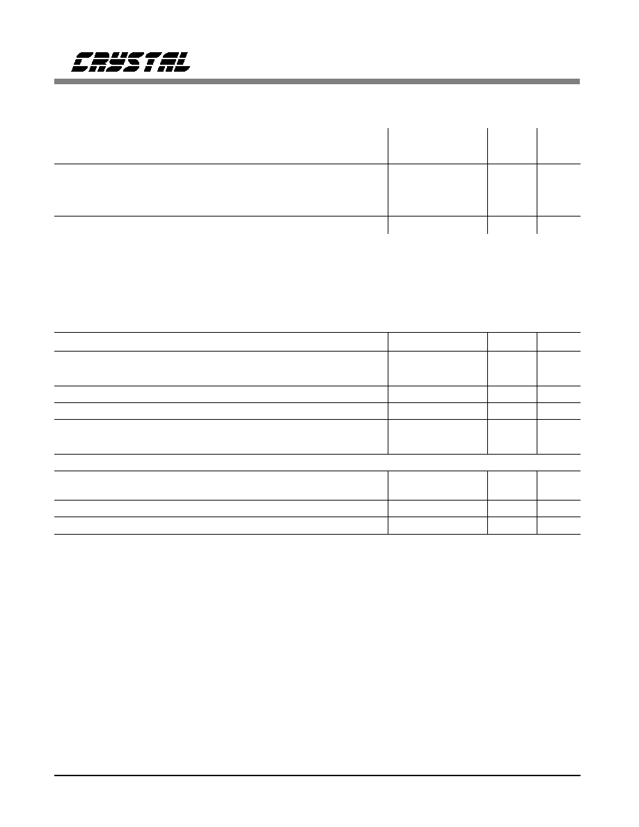
ANALOG CHARACTERISTICS
(T
A
= 25
�
C; VA+ = 5V; -1 dBFS Input Sinewave, 997 Hz;
Fs = 48 kHz; MCLK = 12.288 MHz; SCLK = 3.072 MHz; Measurement Bandwidth is 10 Hz to 20 kHz unless oth-
erwise specified; Logic 0 = 0V, Logic 1 = VD+)
Parameter Symbol
5330A/31A-KS
Min Typ Max
5330A/31A-BS
Min Typ Max Units
Temperature Range T
A
-10 to +70 -40 to +85 �C
Dynamic Performance
Dynamic Range A-weighted 88 94 -
86 92 -
86 94 -
84 92 -
dB
dB
Total Harmonic Distortion+Noise (Note 1)
-1dB
-20dB
-60dB
THD+N
- -84 75
- -72 66
- -32 26
- -84 75
- -72 66
- -32 26
dB
dB
dB
Total Harmonic Distortion -1dB THD - 0.003 0.02 - 0.003 0.02 %
Interchannel Phase Deviation - 0 - - 0 - Degree
Interchannel Isolation
(dc to 20 kHz) - 90 - - 90 - dB
dc Accuracy
Interchannel Gain Mismatch - 0.1 - - 0.1 - dB
Gain Error -
-
�
10 - -
�
10 %
Gain Drift - 150 - - 150 - ppm/
�
C
Offset Error (Note 2) - - 0 - - 0 LSB
Analog Input
Full Scale Input Voltage Range VIN 3.6 4.0 4.4 3.6 4.0 4.4 Vpp
Input Impedance (Fs = 48 kHz) ZIN - 100 - - 100 - k
Input Bias Voltage - 2.4 - - 2.4 - V
Power Supplies
Power Supply Current (Note 3)
VA+
Power down
IA+
-
30
42
- 100 1000
-
30
42
- 100 1000
mA
�
A
Power Dissipation (Note 3)
Normal
Power Down
- 150 220
- 0.5 5.25
- 150 220
- 0.5 5.25
mW
mW
Power Supply Rejection Ratio PSRR - 50 - - 50 - dB
* Refer to Parameter Definitions at the end of this data sheet.
Notes:
1. Referenced to typical full-scale input voltage (4.0 Vpp)
2. Internal highpass filter removes offset.
3. For max power calculations, VD = 5.25 V.
CS5330A/CS5331A
2 DS138F2
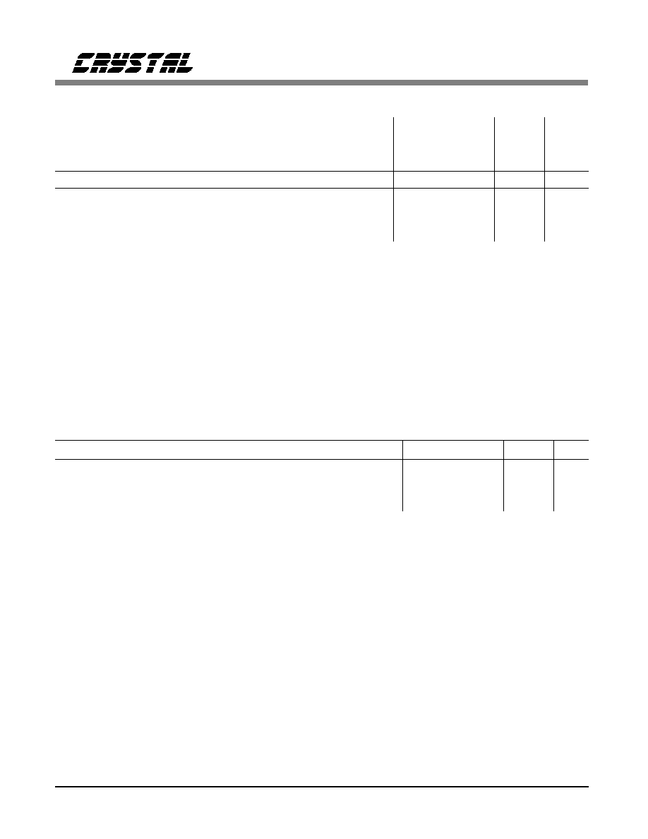
DIGITAL FILTER CHARACTERISTICS
(T
A
= 25
�
C; VA+ = 5V
�
5%; Fs = 48 kHz)
Parameter Symbol Min Typ Max Units
Passband (0.05 dB) (Note 4) 0.02 - 21.7 kHz
Passband Ripple - -
�
0.05 dB
Stopband (Note 4) 29 - 6115 kHz
Stopband Attenuation (Note 5) 80 - - dB
Group Delay (Note 6) t
gd
- 15/Fs - s
Group Delay Variation vs. Frequency
t
gd
-
-
0
�
s
High Pass Filter Characteristics
Frequency Response: -3 dB (Note 4)
-0.1 dB
-
-
3.7
20
-
-
Hz
Hz
Phase Deviation @ 20 Hz (Note 4) - 10 - Degree
Passband Ripple - - 0 dB
Notes:
4. Filter characteristics scale with output sample rate.
5. The analog modulator samples the input at 6.144 MHz for an output sample rate of 48 kHz. There is
no rejection of input signals which are multiples of the sampling frequency ( n x 6.144 MHz
�
21.7kHz
where n = 0,1,2,3...).
6. Group delay for Fs = 48kHz, t
gd
= 15/48kHz = 312
�
s
DIGITAL CHARACTERISTICS
(T
A
= 25
�
C; VA+ = 5V
�
5%)
Parameter Symbol Min Typ Max Units
High-Level Input Voltage V
IH
2.4 - - V
Low-Level Input Voltage V
IL
-
-
0.8
V
High-Level Output Voltage at lo = -20
�
A V
OH
(VD+)-1.0 - - V
Low-Level Output Voltage at lo = 20
�
A V
OL
-
-
0.4
V
Input Leakage Current I
in
-
-
�
10.0
�
A
CS5330A/CS5331A
DS138F2 3
ABSOLUTE MAXIMUM RATINGS
(AGND = 0V, all voltages with respect to ground.)
Parameter Symbol Min Typ Max Units
DC Power Supply: VA+ -0.3 - +6.0 V
Input Current, Any Pin Except Supplies (Note 7) Iin - -
�
10 mA
Analog Input Voltage (Note 8) V
INA
-0.7 - (VA+)+0.7 V
Digital Input Voltage (Note 8) V
IND
-0.7 - (VA+)+0.7 V
Ambient Temperature (power applied) T
A
-55 - +125
�
C
Storage Temperature T
stg
-65 - +150
�
C
Notes:
7. Any Pin except supplies. Transient currents of up to +/- 100 mA on the analog input pins will not
cause SCR latch-up.
8. The maximum over/under voltage is limited by the input current.
WARNING: Operation at or beyond these limits may result in permanent damage to the device.
Normal operation is not guaranteed at these extremes.
RECOMMENDED OPERATING CONDITIONS
(AGND = 0V; all voltages with respect to ground)
Parameter Symbol Min Typ Max Units
DC Power Supplies: VA+ 4.75 5.0 5.25 V
Analog Input Voltage (Note 9) V
IN
-
4
-
Vpp
Analog Input Bias Voltage 2.2 2.4 2.6 V
Note: 9. The output codes will clip at full scale with input signals > Full Scale and < VA+.
Specifications are subject to change without notice.
CS5330A/CS5331A
4 DS138F2
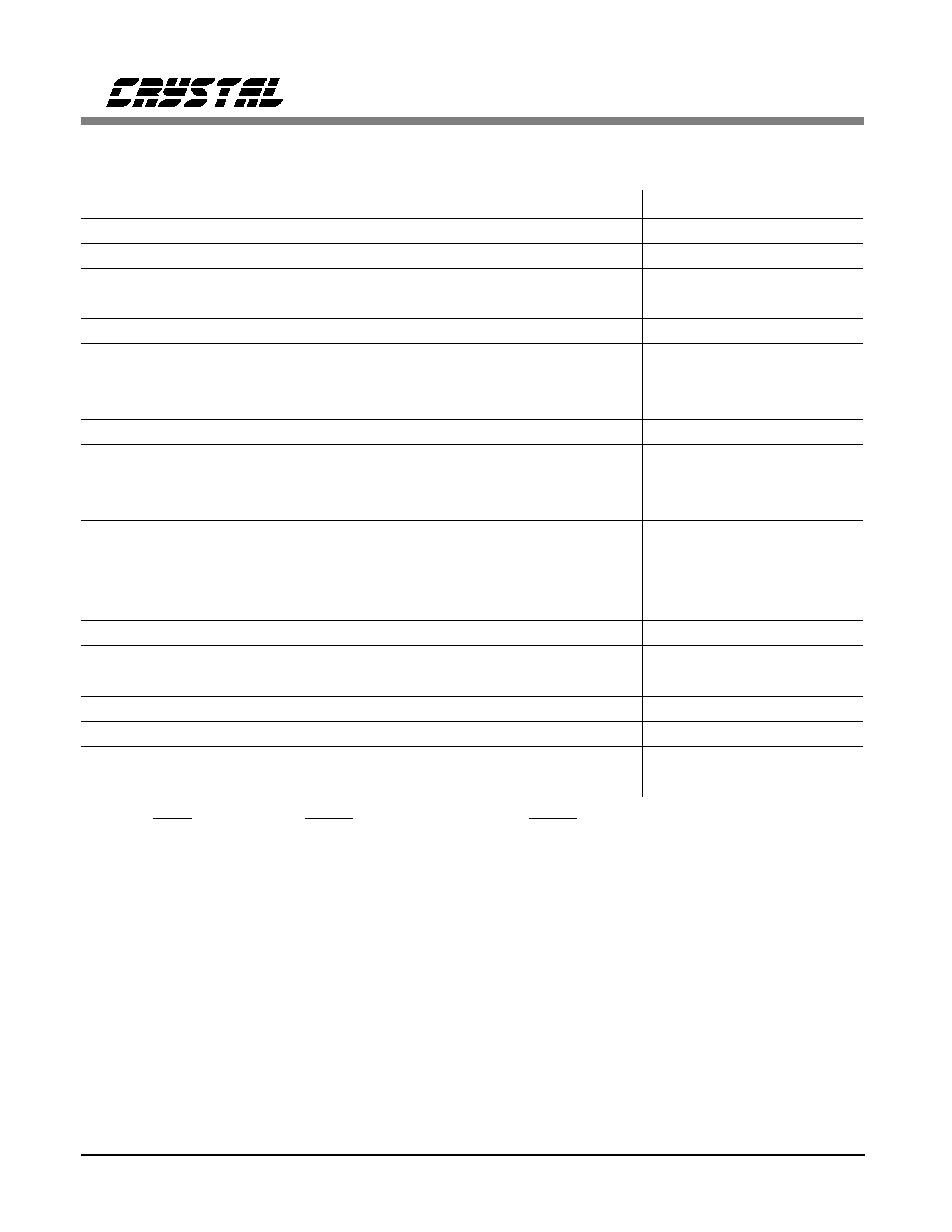
SWITCHING CHARACTERISTICS
(T
A
= 25
�
C; VA+ = 5V
�
5%; Inputs: Logic 0 = 0V, Logic
1 = VA+; C
L
= 20 pF) Switching characteristics are guaranteed by characterization.
Parameter Symbol Min Typ Max Units
Output Sample Rate Fs 2 - 50 kHz
MCLK Period MCLK / LRCK = 256 t clkw
78 1000 ns
MCLK Low MCLK / LRCK = 256 t clkl
31 - 1000 ns
MCLK High MCLK / LRCK = 256 t clkh
31 - 1000 ns
MCLK Period MCLK / LRCK = 384 t clkw
52 1000 ns
MCLK Low MCLK / LRCK = 384 t clkl
20 - 1000 ns
MCLK High MCLK / LRCK = 384 t clkh
20 - 1000 ns
MCLK Period MCLK / LRCK = 512 t clkw
39 1000 ns
MCLK Low MCLK / LRCK = 512 t clkl
13 - 1000 ns
MCLK High MCLK / LRCK = 512 t clkh
13 - 1000 ns
MASTER MODE
SCLK falling to LRCK t mslr
-10 - 10 ns
SCLK falling to SDATA valid t sdo
-10 - 35 ns
SCLK Duty cycle - 50 - %
SLAVE MODE
LRCK duty cycle 25 50 75 %
SCLK Period t sclkw
(Note 10) - - ns
SCLK Pulse Width Low t sclkl
(Note 11) - - ns
SCLK Pulse Width High t sclkh
20 - - ns
SCLK falling to SDATA valid t dss
- - (Note 12) ns
LRCK edge to MSB valid t lrdss
- - (Note 12) ns
SCLK rising to LRCK edge delay t slr1
20 - - ns
LRCK edge to rising SCLK setup time t slr2 (Note 12) - - ns
Notes: 10.
1
64 F
s
11.
1
128 F
s
-
15 ns 12.
1
256 F
s
+
5 ns
CS5330A/CS5331A
DS138F2 5