 | –≠–ª–µ–∫—Ç—Ä–æ–Ω–Ω—ã–π –∫–æ–º–ø–æ–Ω–µ–Ω—Ç: CS5334 | –°–∫–∞—á–∞—Ç—å:  PDF PDF  ZIP ZIP |
Document Outline
- CS5334 CS5335 20-Bit, Stereo A/D Converter for Digital Audio
- Features
- General Description
- ORDERING INFORMATION:
- CHARACTERISTICS & SPECIFICATIONS
- ANALOG CHARACTERISTICS
- Dynamic Performance
- dc Accuracy
- Analog Input
- Power Supplies
- DIGITAL FILTER CHARACTERISTICS
- High Pass Filter Characteristics
- DIGITAL CHARACTERISTICS
- ABSOLUTE MAXIMUM RATINGS
- SWITCHING CHARACTERISTICS
- MASTER MODE
- SCLK to SDATA & LRCK - MASTER mode Format 0 and 1
- SCLK to SDATA & LRCK - MASTER mode Format 2
- SLAVE MODE
- SCLK to LRCK & SDATA - SLAVE mode Format 0 & 1
- SCLK to LRCK & SDATA - SLAVE mode Format 2
- TYPICAL CONNECTION DIAGRAM
- Figure 1. Typical Connection Diagram
- SYSTEM DESIGN
- Table 1. Common Clock Frequencies
- Master Clock
- SERIAL DATA INTERFACE
- Table 2. Digital Input Formats
- Serial Data
- Figure 2. Data Block and Frame
- Figure 3. Serial Data Format 0
- Figure 4. Serial Data Format 1
- Figure 5. Serial Data Format 2
- Serial Clock
- Left / Right Clock
- Master Mode
- Slave Mode
- Analog Connections
- Figure 6. Full Scale Input Levels
- High Pass Filter
- INPUT LEVEL MONITORING
- High Resolution Mode
- Bar Graph Mode
- Overflow
- Initialization
- Initialization with High Pass Filter Enabled
- Initialization and Internal Calibration with High Pass Filter Disabled
- Power-Down
- Grounding and Power Supply Decoupling
- Digital Filter
- Figure 7. CS5334/5 Digital Filter Stopband Rejection
- Figure 8. CS5334/5 Digital Filter Transition Band
- Figure 9. CS5334/5 Digital Filter Passband Ripple
- Figure 10.CS5334/5 Digital Filter Transition Band
- PIN DESCRIPTIONS
- Power Supply Connections
- Analog Inputs
- Analog Outputs
- Digital Inputs
- Digital Inputs / Outputs
- Digital Outputs
- PARAMETER DEFINITIONS
- PACKAGE DIMENSIONS

Features
∑
CS5334
Dynamic Range: 100 dB
THD+N: -90 dB
∑
CS5335
Dynamic Range: 105 dB
THD+N: -95 dB
∑
128X Oversampling
∑
Fully Differential Inputs
∑
Linear Phase Digital Anti-Alias Filtering
21.7 kHz passband (fs = 48kHz)
85 dB stop band attenuation
0.0025 dB pass band ripple
∑
High Pass Filter - DC offset removal
∑
Peak Signal Level Detector
High Resolution and Bar Graph Modes
General Description
The CS5334 and CS5335 are 2-channel, single +5V
supply, pin compatable analog-to-digital converters for
digital audio systems. The CS5334 and CS5335 perform
sampling, analog-to-digital conversion and anti-alias fil-
tering, generating 20-bit values for both left and right
inputs in serial form. The output word rate can be up to
50 kHz per channel.
The CS5334 and CS5335 use 4th-order, delta-sigma
modulation with 128X oversampling followed by digital
filtering and decimation, which removes the need for an
external anti-alias filter. These ADCs use a differential
architecture which provides excellent noise rejection.
The CS5334 and CS5335 have a filter passband to
21.7kHz. The filter has linear phase, 0.0025 dB pass-
band ripple, and >85 dB stopband rejection. An on-chip
high pass filter is also included to remove DC offsets.
ORDERING INFORMATION:
Model
Temp. Range
Package Type
CS5334-KS
-10∞ to 70∞C 20-pin Plastic SSOP
CS5335-KS
-10∞ to 70∞C 20-pin Plastic SSOP
Crystal Semiconductor Corporation
P.O. Box 17847, Austin, TX 78760
(512) 445 7222 FAX: (512) 445 7581
http://www.crystal.com
NOV '96
DS237PP2
1
20-Bit, Stereo A/D Converter for Digital Audio
S/H
S/H
Voltage Reference
Comparator
Comparator
VA+
PU
DAC
DAC
LP Filter
LP Filter
VD+
DGND
MCLK
Digital Decimation
Filter
Digital Decimation
Filter
Serial Output Interface
SDATA
AINR-
AGND
AINL-
AINL+
AINR+
High Pass
Filter
High Pass
Filter
DIF1
DIF0
FRAME SCLK LRCK
HP DEFEAT
CMOUT
OVFL
11
7
2
8
12
9
20
19
1
5
6
4
13
14
17
16
15
3
10
RST
18
CS5334 CS5335
This document contains information for a new product. Crystal
Semiconductor reserves the right to modify this product without notice.
Preliminary Product Information
Copyright
©
Crystal Semiconductor Corporation 1996
(All Rights Reserved)
Specifications are subject to change without notice
ANALOG CHARACTERISTICS
(T
A
= 25
∞
C; VA+ = VD+ = 5V; -1 dBFS Input Sinewave, 997 Hz;
Fs = 48 kHz; MCLK = 12.288 MHz; SCLK = 3.072 MHz; Measurement Bandwidth is 10 Hz to 20 kHz unless
otherwise specified; Logic 0 = 0V, Logic 1 = VD+)
CS5334
CS5335
Parameter
Symbol
Min
Typ
Max
Min
Typ
Max
Units
Resolution
20
-
-
20
-
-
Bits
Dynamic Performance
Dynamic Range
A-weighted
TBD
TBD
100
97
-
-
TBD
TBD
105
102
-
-
dB
dB
Total Harmonic Distortion + Noise
-1 dB
-20 dB
-60 dB
THD+N
-
-
-
-90
-77
-37
TBD
TBD
TBD
-
-
-
-95
-82
-42
TBD
TBD
TBD
dB
dB
dB
Interchannel Phase Deviation
-
0.01
-
-
0.01
-
Degree
Interchannel Isolation
(dc to 20 kHz)
-
100
-
-
105
-
dB
dc Accuracy
Interchannel Gain Mismatch
-
0.05
-
-
0.05
-
dB
Gain Error
-
-
±
5
-
-
±
5
%
Gain Drift
-
200
-
-
200
-
ppm/∞C
Offset Error
with HPF
HP defeat with CAL
-
-
0
+/-
100
-
-
-
-
0
+/-
100
-
-
LSB
LSB
Analog Input
Input Voltage Range
(Differential)
VIN
1.9
2.0
2.1
1.9
2.0
2.1
Vrms
Input Impedance
ZIN
-
30
-
-
30
-
k
Input Bias Voltage
-
2.2
-
-
2.2
-
V
Power Supplies
Power Supply Current
IA
ID
Power Down (IA+ID)
-
-
-
38
25
0.2
TBD
TBD
-
-
-
-
40
25
0.2
TBD
TBD
-
mA
mA
mA
Power Dissipation
Normal
Power Down
-
-
315
1.0
TBD
-
-
-
325
1.0
TBD
-
mW
mW
Power Supply Rejection Ratio
-
50
-
-
55
-
dB
CS5334 CS5335
2
DS237PP2

DIGITAL FILTER CHARACTERISTICS
(T
A
= 25
∞
C; VA+ = VD+ = 5V
±
5%; Fs = 48 kHz)
Parameter
Symbol
Min
Typ
Max
Units
Passband
(Note 1)
0.02
-
21.7
kHz
Passband Ripple
-
-
±
0.0025
dB
Stopband
(Note 1)
26.3
-
6118
kHz
Stopband Attenuation
(Note 2)
85
-
-
dB
Group Delay (Fs = Output Sample Rate)
t
gd
-
32/Fs
-
s
Group Delay Variation vs. Frequency
t
gd
-
-
0
µ
s
High Pass Filter Characteristics
Frequency Response:
-3 dB
(Note 1)
-0.01 dB
-
-
0.9
20
-
-
Hz
Hz
Phase Deviation
@ 20 Hz
(Note 1)
-
2.6
-
Degree
Passband Ripple
-
-
0
dB
Notes:
1. Filter characteristic scales with output sample rate.
2. The analog modulator samples the input at 6.144 MHz for an output sample rate of 48 kHz. There is
no rejection of input signals which are multiples of the sampling frequency ( n x 6.144 MHz
±
21.7kHz
where n = 0,1,2,3...).
DIGITAL CHARACTERISTICS
(T
A
= 25
∞
C; VA+ = VD+ = 5V
±
5%)
Parameter
Symbol
Min
Typ
Max
Units
High-Level Input Voltage
V
IH
2.4
-
-
V
Low-Level Input Voltage
V
IL
-
-
0.8
V
High-Level Output Voltage at lo = -20
µ
A
V
OH
(VD+)-1.0
-
-
V
Low-Level Output Voltage at lo = 20
µ
A
V
OL
-
-
0.4
V
Input Leakage Current
I
in
-
-
10
µ
A
ABSOLUTE MAXIMUM RATINGS
(AGND = 0V, all voltages with respect to ground.)
Parameter
Symbol
Min
Typ
Max
Units
DC Power Supply:
VA+
-0.3
-
+6.0
V
Input Current, Any Pin Except Supplies
(Note 3)
Iin
-
-
±
10
mA
Analog Input Voltage
(Note 4)
V
INA
-0.7
-
(VA+)+0.7
V
Digital Input Voltage
(Note 4)
V
IND
-0.7
-
(VA+)+0.7
V
Ambient Temperature (power applied)
T
A
-55
-
+125
∞
C
Storage Temperature
T
stg
-65
-
+150
∞
C
Notes:
3. Any Pin except supplies. Transient currents of up to +/- 100 mA on the analog input pins will not
cause SCR latch-up.
4. The maximum over/under voltage is limited by the input current.
WARNING:Operation at or beyond these limits may result in permanent damage to the device.
Normal operation is not guaranteed at these extremes.
CS5334 CS5335
DS237PP2
3

SWITCHING CHARACTERISTICS
(T
A
= 25
∞
C; VA+ = 5V
±
5%; Inputs: Logic 0 = 0V, Logic 1 = VA+ = VD+; C
L
= 20 pF)
Parameter
Symbol
Min
Typ
Max
Units
Output Sample Rate
F
s
2.0
-
50
kHz
MCLK Period
MCLK / LRCK = 256
t clkw
78
-
1953
ns
MCLK Low
MCLK / LRCK = 256
t clkl
31
-
-
ns
MCLK High
MCLK / LRCK = 256
t clkh
31
-
-
ns
MCLK Period
MCLK / LRCK = 384
t clkw
52
-
1302
ns
MCLK Low
MCLK / LRCK = 384
t clkl
20
-
-
ns
MCLK High
MCLK / LRCK = 384
t clkh
20
-
-
ns
MCLK Period
MCLK / LRCK = 512
t clkw
39
-
976
ns
MCLK Low
MCLK / LRCK = 512
t clkl
15
-
-
ns
MCLK High
MCLK / LRCK = 512
t clkh
15
-
-
ns
MASTER MODE
SCLK falling to LRCK
(Note 5)
t mslr
-10
-
10
ns
SCLK falling to SDATA valid
(Note 5)
t sdo
-10
-
35
ns
SCLK Duty cycle
-
50
-
%
SCLK falling to Frame Valid
(Note 5)
t sfo
-10
-
(Note 6)
ns
LRCK edge to OVFL Valid
t ovfl
-10
-
30
ns
LRCK edge to OVFL edge delay
t ovfl
-10
-
(Note 10)
ns
SLAVE MODE
LRCK duty cycle
25
50
75
%
SCLK Period
t sclkw
(Note 7)
-
-
ns
SCLK Pulse Width Low
(Note 8)
t sclkl
(Note 11)
-
-
ns
SCLK Pulse Width High
(Note 9)
t sclkh
50
-
-
ns
SCLK falling to SDATA valid
(Note 5)
t dss
-
-
(Note 11)
ns
LRCK edge to MSB valid
t lrdss
-
-
(Note 11)
ns
SCLK rising to LRCK edge delay
(Note 12)
t slr1
50
-
-
ns
LRCK edge to rising SCLK setup time
(Note 12)
t slr2
(Note 11)
-
-
ns
SCLK falling to Frame delay
t sfo
-
-
(Note 13)
ns
Notes: 5. SCLK rising for Mode 1.
6.
1
(
1024
)(
F
s
)
+
30ns
7.
1
(
96
)(
F
s
)
8. Pulse Width High for Mode 1
9. Pulse Width Low for Mode 1
10.
1
(
512
)(
F
s
)
+
20ns
11.
1
(
512
)(
F
s
)
+
50ns
12. SCLK Falling for Mode 1
13.
1
(
384
)(
F
s
)
+
35ns
CS5334 CS5335
4
DS237PP2
SDATA
SCLK input
(SLAVE mode)
(SLAVE mode)
LRCK input
sclkh
t
dss
t
MSB
MSB-1
sclkl
t
slr1
t
slr2
t
tsclkw
OVFL
tovfl
SCLK to LRCK & SDATA - SLAVE mode
Format 2
SCLK output
tmslr
SDATA
tsdo
LRCK output
MSB
tovfl
OVFL
SCLK to SDATA & LRCK - MASTER mode
Format 2
SCLK output*
tmslr
SDATA
tsdo
LRCK output
tovfl
OVFL
MSB
MSB-1
SCLK to SDATA & LRCK - MASTER mode
Format 0 and 1
SDATA
SCLK input*
(SLAVE mode)
(SLAVE mode)
LRCK input
sclkh
t
dss
t
MSB
MSB-1
MSB-2
lrdss
t
sclkl
t
slr1
t
slr2
t
t sclkw
OVFL
ovfl
t
SCLK to LRCK & SDATA - SLAVE mode
Format 0 & 1
SCLK*
FRAME
tsfo
SCLK to Frame Delay
*SCLK is inverted for Format 1
CS5334 CS5335
DS237PP2
5

+
1
µ
F
0.1
µ
F
2
+
1
µ
F
0.1
µ
F
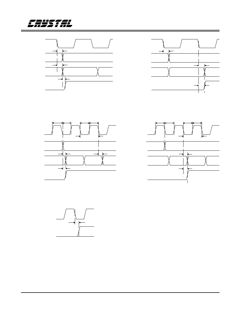
+5V Analog
VD+
VA+
6
3
2.2 nF
150
150
Left Analog
Input +
Left Analog
Input -
17
16
2.2 nF
150
150
Right Analog
Input +
Right Analog
Input -
13
14
15
AINL+
AINL-
CMOUT
AINR+
AINR-
2
11
Peak Signal
Level Monitor
1
20
Mode
Settings
19
18
9
Audio Data
Processing
12
8
Timing, Logic
&
Clock
10
7
OVFL
PU
HP DEFEAT
DIF0
DIF1
RST
LRCK
SCLK
FRAME
MCLK
SDATA
DGND
AGND
5
4
CS5334
CS5335
A/D Converter
47 k
*
47 k
**
Required for Master Mode only
Required for Bar Graph Mode only
*
**
100
100
100
100
Figure 1. Typical Connection Diagram
CS5334 CS5335
6
DS237PP2

SYSTEM DESIGN
The CS5334 and CS5335 are 20-bit, 2-channel
Analog-to-Digital Converters designed for digital
audio applications. These devices use two one-
bit delta-sigma modulators which simultaneously
sample the analog input signals at 128 times the
output sample rate (Fs). The resulting serial bit
streams are digitally filtered, yielding a pair of
20-bit values. This technique yields nearly ideal
conversion performance independent of input
frequency and amplitude. The converter does not
require difficult-to-design or expensive anti-alias
filters and does not require external sample-and-
hold amplifiers or a voltage reference. Very few
external components are required to support
these ADCs. Normal power supply decoupling
components and a resistor and capacitor on each
input for anti-aliasing are all that's required, as
shown in Figure 1.
An on-chip voltage reference provides for a dif-
ferential input signal range of 2.0 Vrms. Output
data is available in serial form, coded as
2's complement, 20-bit numbers. Typical power
consumption is 325 mW which can be reduced
to 1.0 mW using the power-down feature.
Master Clock
The master clock (MCLK) is the clock source
for the delta-sigma modulator sampling and digi-
tal filters. In Master Mode, the frequency of this
clock must be 256
◊
Fs. In Slave Mode, the mas-
ter clock must be either 256
◊, 384◊
or 512
◊
Fs.
Table 1 shows some common master clock fre-
quencies.
SERIAL DATA INTERFACE
The CS5334 and CS5335 support three serial
data formats, including I
2
S, which are selected
via the digital input format pins DIF0 and DIF1.
The digital input format determines the relation-
ship between the serial data, left/right clock and
serial clock. Table 2 lists the three formats, along
with the associated figure number. The serial
data interface is accomplished via the serial data
output, SDATA, serial data clock, SCLK, and the
left/right clock, LRCK.
Serial Data
The serial data block consists of 20 bits of audio
data presented in 2's-complement format with
the MSB-first, followed by 4 bits of zero and 8
Peak Signal Level, PSL, bits as shown in Fig-
ure 2. The data is clocked from SDATA by the
serial clock and the channel is determined by the
Left/Right clock.
LRCK
(kHz)
MCLK (MHz)
256 X
384 X
512 X
32
8.1920
12.2880
16.3840
44.1
11.2896
16.9344
22.5792
48
12.2880
18.4320
24.5760
Table 1. Common Clock Frequencies
SDATA
FRAME
P7
19 18
1
0
P6
P1 P0
20 Audio
Data Bits
4 Zeros
8 PSL Bits
Figure 2. Data Block and Frame
DIF1
DIF0
FORMAT
FIGURE
0
0
0
3
0
1
1
4
1
0
2
5
1
1
power-down
-
Table 2. Digital Input Formats
CS5334 CS5335
DS237PP2
7

SDATA
P1 P0
19 18
1
P7 P6 P5 P4 P3 P2
0
19 18
FRAME
SCLK
LRCK
P1 P0
19 18
1
P7 P6 P5 P4 P3 P2
0
MASTER
SLAVE
20-Bit Left Justified Data
20-Bit Left Justified Data
Data Valid on Rising Edge of 64x SCLK
Data Valid on Rising Edge of SCLK
MCLK equal to 256x F
s
MCLK equal to 256x, 384x or 512x F
s
Figure 3. Serial Data Format 0
SDATA
P1 P0
19 18
1
P7 P6 P5 P4 P3 P2
0
19 18
FRAME
SCLK
LRCK
P1 P0
19 18
1
P7 P6 P5 P4 P3 P2
0
MASTER
SLAVE
20-Bit Left Justified Data
20-Bit Left Justified Data
Data Valid on Falling Edge of 64x SCLK
Data Valid on Falling Edge of SCLK
MCLK equal to 256x F
s
MCLK equal to 256x, 384x or 512x F
s
Figure 4. Serial Data Format 1
SDATA
P1 P0
19 18
1
P7 P6 P5 P4 P3 P2
0
19 18
FRAME
SCLK
LRCK
P1 P0
19 18
1
P7 P6 P5 P4 P3 P2
0
MASTER
SLAVE
I
2
S 20-Bit Data
I
2
S 20-Bit Data
Data Valid on Rising Edge of 64x SCLK
Data Valid on Rising Edge of SCLK
MCLK equal to 256x F
s
MCLK equal to 256x, 384x or 512x F
s
Figure 5. Serial Data Format 2
CS5334 CS5335
8
DS237PP2

Serial Clock
The serial clock shifts the digitized audio data
from the internal data registers via the
SDATA pin. SCLK is an output in Master Mode.
Internal dividers will divide the master clock by
4 to generate a serial clock which is 64
◊
Fs. In
Slave Mode, SCLK is an input with a serial
clock typically between 4
8◊
and 128
◊
Fs. How-
ever, the serial clock must be a minimum of 64
◊
Fs to access the Peak Signal Level bits.
Left / Right Clock
The Left/Right clock determines which channel,
left or right, is to be output on SDATA. Although
the outputs for each channel are transmitted at
different times, Left/Right pairs represent simul-
taneously sampled analog inputs. In Master
Mode, LRCK is an output whose frequency is
equal to Fs. In Slave Mode, LRCK is an input
whose frequency must be equal to the output
sample rate, Fs.
Master Mode
In Master mode, SCLK and LRCK are outputs
which are internally derived from the Master
Clock. Internal dividers will divide MCLK by 4
to generate a SCLK which is 64
◊
Fs and by 256
to generate a LRCK which is equal to Fs. Master
mode is only supported with a 256
◊
master
clock. The CS5334/5 is placed in the Master
mode with a 47 k
pull-down resistor on the
OVFL pin.
Slave Mode
LRCK and SCLK become inputs in SLAVE
mode. LRCK must be externally derived from
MCLK and be equal to Fs. The serial clock is
typically between 64
◊
and 128
◊
Fs. A 48
◊
Fs
serial clock is possible though will not allow ac-
cess to the Peak Signal Level bits. Master clock
frequencies of 256
◊
, 384
◊
and 512
◊
Fs are sup-
ported. The ratio of the applied master clock to
the left/right clock is automatically detected dur-
ing power-up and internal dividers are set to gen-
erate the appropriate internal clocks.
Analog Connections
Figure 1 shows the analog input connections.
The analog inputs are presented to the modula-
tors via the AINR+/- and AINL+/- pins. Each
analog input pin will accept a maximum of
1 Vrms centered at +2.2 Volt as shown in Fig-
ure 6. Input signals can be AC or DC coupled
and the CMOUT output may be used as a refer-
ence for DC coupling. However, CMOUT is not
buffered and the maximum current is 10
µ
A.
The CS5334 and CS5335 sample the analog in-
puts at 128
◊
Fs, 6.144 MHz for a 48 kHz
sample-rate. The digital filter rejects all noise
above 26.3 kHz except for frequencies right
around 6.144 MHz
±
21.7 kHz (and multiples of
6.144 MHz). Most audio signals do not have sig-
nificant energy at 6.144 MHz. Nevertheless, a
150
resistor in series with each analog input
and a 2.2 nF capacitor across the inputs will at-
tenuate any noise energy at 6.144
MHz, in
addition to providing the optimum source imped-
ance for the modulators. The use of capacitors
which have a large voltage coefficient must be
avoided since these will degrade signal linearity.
NPO and COG capacitors are acceptable. If ac-
tive circuitry precedes the ADC, it is
recommended that the above RC filter is placed
between the active circuitry and the AINR and
AINL pins. The above example frequencies scale
linearly with sample rate.
3.6 V
2.2 V
0.78 V
3.6 V
2.2 V
0.78 V
CS5334
CS5335
AIN+
AIN-
Full Scale Input level= (AIN+) - (AIN-)= 5.67 Vpp
Figure 6. Full Scale Input Levels
CS5334 CS5335
DS237PP2
9

High Pass Filter
The operational amplifiers in the input circuitry
driving the CS5334/5 may generate a small DC
offset into the A/D converter. The CS5334 and
CS5335 include a high pass filter after the deci-
mator to remove any DC offset which could
result in recording a DC level, possibly yielding
"clicks" when switching between devices in a
multichannel system. The high pass filter can be
disabled with the HP DEFEAT pin. The high
pass filter works by continuously subtracting a
measure of the dc offset from the output of the
decimation filter. If the HP DEFEAT pin is
taken high during normal operation, the current
value of the dc offset register is frozen and this
dc offset will continue to be subtracted from the
conversion result. This feature makes it possible
to perform a system calibration by;
1. removing the signal source (or grounding the
input signal) at the input to the subsystem con-
taining the CS5334/5,
2. running the CS5334/5 with the HP DEFEAT
pin low (high pass filter enabled) until the filter
settles (approximately 1 second), and
3. taking the HP DEFEAT pin high, disabling
the high pass filter and freezing the stored dc
offset.
A system calibration performed in this way will
eliminate offsets anywhere in the signal path be-
tween the calibration point and the CS5334/5.
The characteristics of the first-order high pass
filter are outlined below for an output sample
rate of 48 kHz. This filter response scales line-
arly with sample rate.
Frequency response: -3 dB @ 0.9 Hz
-0.01 dB @ 20 Hz
Phase deviation:
2.6 degrees @ 20 Hz
Passband ripple:
None
INPUT LEVEL MONITORING
The CS5334 and CS5335 include independent
Peak Input Level Monitoring for each channel.
The analog-to-digital converter continually moni-
tors the peak digital signal for both channels,
prior to the digital limiter, and records these val-
ues in the Active registers. This information can
be transferred to the Output registers by a high
to low transition on the Peak Update pin (PU)
which will also reset the Active register. The Ac-
tive register contains the peak signal level since
the previous peak update request.
The 8-bit contents of the output registers are
available in all interface modes and are present
in the data block as shown in Figure 2. The
monitoring function can be formatted to indicate
either High Resolution Mode or Bar Graph
Mode. The monitoring function is determined on
power-up by the presence of a 47 kohm pull-
down resistor on FRAME. The addition of a
47 kohm pull-down resistor on the FRAME pin
sets the monitoring function to the Bar Graph
mode.
High Resolution Mode
Bits P7-P0 indicate the peak input level since the
previous peak update (or low transition on the
Peak Update pin). If the full scale input level is
exceeded (Bit P7 high), bits P5-P0 represent the
peak value up to 3 dB above full-scale in 1 dB
steps. If the ADC input level is less than full-
scale, bits P5-P0 represent the peak value from
-60 dB to 0 dB of full scale in 1 dB steps. The
PSL outputs are accurate to within 0.25 dB. Bit
P6 provides a coarse means of determining an
ADC input idle condition. Bit P7 indicates an
ADC overflow condition, if the ADC input level
is greater than full-scale.
CS5334 CS5335
10
DS237PP2

P7 - Overrange
0 - Analog input less than full-scale level
1 - Analog input greater than full-scale
P6 - Idle channel
0 - Analog input >-60 dB from full-scale
1 - Analog input <-60 dB from full-scale
P5 to P0 - Peak Signal Level Bits (1 dB steps)
Inputs <0 dB
P5 - P0
0 dB
000000
-1 dB
000001
-2 dB
000010
-60 dB
111100
Inputs >0 dB
P5 - P0
0 dB
000000
+1 dB
000001
+2 dB
000010
+3 dB
000011
Bar Graph Mode
This mode provides a decoded output format
which indicates the peak Peak Signal Level in a
"Bar Graph" format.
Input Level
P7 - P0
Overflow
11111111
0 dB to -3 dB
01111111
-3 dB to -6 dB
00111111
-6 dB to -10 dB
00011111
-10 dB to -20 dB
00001111
-20 dB to -30 dB
00000111
-30 dB to -40 dB
00000011
-40 dB to -60 dB
00000001
< - 60 dB
00000000
Overflow
Overflow indicates analog input overrange, for
both the Left and Right channels, since the last
update request on the Peak Update pin. A value
of 1 indicates an overrange condition. The left
channel information is output on OVFL during
the left channel portion of LRCK. The right
channel information is available on OVFL during
the right channel portion of LRCK.
Initialization
Upon initial power-up, the digital filters and
delta-sigma modulators are reset and the internal
voltage reference is powered down. The
CS5334/5 will remain in the power-down mode
until valid clocks are presented. A valid MCLK
is required to exit power-down in Master Mode.
However, in Slave Mode, MCLK and LRCK of
the proper ratio are required to exit power-down.
MCLK occurrences are also counted over one
LRCK period to determine the MCLK / LRCK
frequency ratio in Slave Mode. Power is then ap-
plied to the internal voltage reference, the analog
inputs will move to approximately 2.2V and out-
put clocks will begin (Master Mode only). This
process requires 32 periods of LRCK and is fol-
lowed by the initialization sequence.
Initialization with High Pass Filter Enabled
28,672 LRCK cycles are required for the initiali-
zation sequence with the high pass filter enabled.
This time is dominated by the settling time re-
quired for the high pass filter.
Initialization and Internal Calibration with
High Pass Filter Disabled
If the HP DEFEAT pin is high (high pass filter
disabled) during the initialization sequence, the
CS5334/5 will perform an internal dc calibration
by:
1. disconnecting the internal ADC inputs from
the input pins,
2. connecting the (differential) ADC inputs to a
common reference voltage,
CS5334 CS5335
DS237PP2
11

3. running the high pass filter with a fast settling
time constant,
4. freezing the dc offset register, and
5. reconnecting the internal ADC inputs to the
input pins.
This procedure takes 4,160 cycles of LRCK.
Unlike the system calibration procedure de-
scribed in the High Pass Filter section, a dc
calibration performed during start-up will only
eliminate offsets internal to the CS5334/5, and
should result in output codes which accurately
reflect the differential dc signal at the pins.
Power-Down
The CS5334 and CS5335 have a power-down
mode wherein typical consumption drops to 1.0
mW. This is initiated when a loss of clock is de-
tected (either LRCK or MCLK in Slave Mode or
MCLK in Master Mode), RST is enabled or
DIF0 / DIF1 are at a logic 1. The initialization
sequence will begin whenever valid clocks are
restored, RST is disabled and DIF0 / DIF1 are
restored. If the MCLK / LRCK frequency ratio
changes during power-down, the CS5334/5 will
adapt to these new operating conditions. How-
ever, only the RST method of power-down will
include the Master/Slave decision in the initiali-
zation sequence.
Grounding and Power Supply Decoupling
As with any high resolution converter, the
CS5334 and CS5335 require careful attention to
power supply and grounding arrangements to op-
timize performance. Figure 1 shows the
recommended power arrangements with VA+
connected to a clean +5 volt supply. VD+ should
be derived from VA+ through a 2 ohm resistor.
VD+ should not be used to power additional
digital circuitry. All mode pins which require
VD+ should be connected to pin 6 of the
CS5334/5. All mode pins which require DGND
should be connected to pin 5 of the CS5334/5.
AGND and DGND, Pins 4 and 5, should be con-
nected together at the CS5334/5. DGND for the
CS5334/5 should not be confused with the
ground for the digital section of the system. The
CS5334/5 should be positioned over the analog
ground plane near the digital / analog ground
plane split. The analog and digital ground planes
must be connected elsewhere in the system. The
CS5334/5 evaluation board, CDB5334/5, demon-
strates this layout technique. This technique
minimizes digital noise and insures proper power
supply matching and sequencing. Decoupling ca-
pacitors should be located as near to the
CS5334/5 as possible.
CS5334 CS5335
12
DS237PP2

Digital Filter
Figures 7-10 show the performance of the
digital filter included in the CS5334/5. All
plots are normalized to Fs. Assuming a sample
rate of 48 kHz, the 0.5 frequency point on the
plot refers to 24 kHz. The filter frequency re-
sponse scales precisely with the sample rate.
Figure 7. CS5334/5 Digital Filter Stopband Rejection
Figure 9. CS5334/5 Digital Filter Passband Ripple
Figure 8. CS5334/5 Digital Filter Transition Band
Figure 10.CS5334/5 Digital Filter Transition Band
CS5334 CS5335
DS237PP2
13

PIN DESCRIPTIONS
Power Supply Connections
VA+ - Positive Analog Power, Pin 3.
Positive analog supply. Nominally +5 volts.
VD+ - Positive Digital Power, Pin 6.
Positive digital supply. Nominally +5 volts.
AGND - Analog Ground, Pin 4.
Analog ground reference.
DGND - Digital Ground, Pin 5.
Digital ground reference.
Analog Inputs
AINR-, AINR+ - Differential Right Channel Analog Input, Pin 14 and Pin 13.
Analog input connections of the right channel differential inputs. Typically 2 Vrms differential
(1Vrms for each input pin) for a full-scale analog input signal.
AINL-, AINL+ - Differential Left Channel Analog Input, Pin 16 and Pin 17.
Analog input connections of the left channel differential inputs. Typically 2 Vrms differential
(1Vrms for each input pin) for a full-scale analog input signal.
Analog Outputs
CMOUT - Common Mode Output, Pin 15.
This output, nominally 2.2V, can be used to bias the analog input circuitry to the common mode
voltage of the CS5334/5.
1
2
3
4
5
6
7
8
9
20
19
18
17
16
15
14
13
12
10
11
High Pass Filter Defeat HP DEFEAT
DIF0
Digital Interface Format 0
OverFlow OVFL
DIF1
Digital Interface Format 1
Analog Power VA+
RST
Reset
Analog Ground AGND
AINL+
Non-Inverting Left Channel Input
Digital Ground DGND
AINL-
Inverting Left Channel Input
Digital Power VD+
CMOUT Common Mode Output
Master Clock MCLK
AINR-
Inverting Right Channel Input
Serial Data Clock SCLK
AINR+
Non-Inverting Right Channel Input
Serial Data Output SDATA
LRCK
Left/ Right Clock
Frame Signal FRAME
PU
Peak Update
CS5334 CS5335
14
DS237PP2

Digital Inputs
MCLK - Master Clock, Pin 7.
Clock source for the delta-sigma modulator sampling and digital filters.
In Master Mode, the frequency of this clock must be 256
◊
the output sample rate, Fs.
In Slave Mode, the frequency of this clock must be either 256
◊, 384◊
or 512
◊
Fs.
DIF0, DIF1 - Digital Interface Format, Pins 19 and 20.
These two pins select one of 3 digital interface formats or power-down. The format determines
the relationship between SCLK, LRCK and SDATA. The formats are detailed in Figures 3-5.
RST - Reset, Pin 18.
A low logic level on this pin activates Reset.
HP DEFEAT - High Pass Filter Defeat, Pin 1.
A high logic level on this pin disables the digital high pass filter. A low logic level on this pin
enables the high pass filter.
PU - Peak Update, Pin 11.
Transfers the Peak Signal Level contents of the Active Registers to the Output Registers on a
high to low transition on this pin. This transition will also reset the Active register.
Digital Inputs / Outputs
LRCK - Left/Right Clock, Pin 12.
LRCK determines which channel, left or right, is to be output on SDATA. The relationship
between LRCK, SCLK and SDATA is controlled by DIF0 and DIF1. Although the outputs for
each channel are transmitted at different times, Left/Right pairs represent simultaneously
sampled analog inputs. In Master Mode, LRCK is an output clock whose frequency is equal to
the output sample rate, Fs. In Slave Mode, LRCK is an input clock whose frequency must be
equal to Fs.
SCLK - Serial Data Clock, Pin 8.
Clocks the individual bits of the serial data out from the SDATA pin. The relationship between
LRCK, SCLK and SDATA is controlled by DIF0 and DIF1.
In Master Mode, SCLK is an output clock with a frequency of 64x the output sample rate, Fs.
In Slave Mode, SCLK is an input.
Digital Outputs
SDATA - Serial Data Output, Pin 9.
Two's complement MSB-first serial data of 20 bits is output on this pin. Included in the serial
data output is the 8-bit Input Signal Level Bits. The data is clocked out via the SCLK clock and
the channel is determined by LRCK. The relationship between LRCK, SCLK and SDATA is
controlled by DIF0 and DIF1.
CS5334 CS5335
DS237PP2
15

OVFL - Overflow, Pin 2.
Overflow indicates analog input overrange, for both the Left and Right channels, since the last
update request on the PEAK UPDATE (PU) pin. A value of 1 in the register indicates an
overrange condition. The left channel information is output on OVFL during the left channel
portion of LRCK. The right channel information is available on OVFL during the right channel
portion of LRCK. The registers are updated with a high to low transition on the PEAK
UPDATE pin. A 47 kohm pull-down resistor on this pin will set the CS5334/5 in Master Mode.
FRAME - Frame Signal, Pin 10.
Frames the Peak Signal Level (PSL) Bits. FRAME goes high coincident with the leading edge
of the first PSL bit and falls coincident with the trailing edge of the last PSL bit as shown in
Figures 3-5. A 47 kohm pull-down resistor on this pin will set the Peak Signal Level
Monitoring format to "Bar Graph" mode.
PARAMETER DEFINITIONS
Dynamic Range
The ratio of the rms value of the signal to the rms sum of all other spectral components over
the specified bandwidth. Dynamic Range is a signal-to-noise ratio measurement over the
specified band width made with a -60dBFs signal. 60dB is added to resulting measurement to
refer the measurement to full-scale. This technique ensures that the distortion components are
below the noise level and do not effect the measurement. This measurement technique has been
accepted by the Audio Engineering Society, AES17-1991, and the Electronic Industries
Association of Japan, EIAJ CP-307. Expressed in decibels.
Total Harmonic Distortion + Noise (THD+N)
The ratio of the rms value of the signal to the rms sum of all other spectral components over
the specified band width (typically 10 Hz to 20 kHz), including distortion components.
Expressed in decibels. Measured at -1 and -20 dBFs as suggested in AES17-1991 Annex A.
Frequency Response
A measure of the amplitude response variation from 10 Hz to 20 kHz relative to the amplitude
response at 1 kHz. Units in decibels.
Interchannel Isolation
A measure of crosstalk between the left and right channels. Measured for each channel at the
converter's output with no signal at the input under test and a full-scale signal applied to the
other channel. Units in decibels.
Interchannel Gain Mismatch
The gain difference between left and right channels. Units in decibels.
Gain Error
The deviation from the nominal full-scale analog input for a full-scale digital output.
CS5334 CS5335
16
DS237PP2

Gain Drift
The change in gain value with temperature. Units in ppm/
∞
C.
Offset Error
The deviation of the mid-scale transition (111...111 to 000...000) from the ideal. Units in mV.
CS5334 CS5335
DS237PP2
17

PACKAGE DIMENSIONS
E
e
b
A
A1
D
E1
A2
See DETAIL 'A'
L
0.25 BSC
Seating
Plane
Gauge
Plane
3
3
DETAIL 'A'
SIDE VIEW
END VIEW
TOP VIEW
4
Seating Plane
Notes:
1. Dimensioning and tolerance per
ANSI.Y14.5M-1982.
2. Symbols are defined in the "MO
Series Symbol List" in section 2.2
of JEDEC Publication 95.
3. "D" and "E1" are reference datums
and do not include mold flash or
protrusions, but do include mold
mismatch and are measured at the
parting line, mold flash or protrusions
shall not exceed 0.20mm per side.
4. Dimension b does not include
dambar protrusion/intrusion.
Allowable dambar protrusion shall
be 0.13mm total in excess of b
dimension at maximum material
condition. Dambar intrusion shall
not reduce dimension b by more than
0.07mm at least material condition.
5. These dimensions apply to the flat
section of the lead between 0.10 and
0.25mm from lead tips.
N
1
3 2
SSOP
Package Dimensions
N
D
MIN NOM MAX
14
16
20
24
28
30
5.90 6.20 6.50
5.90 6.20 6.50
6.90 7.20 7.50
7.90 8.20 8.50
9.90 10.20 10.50
9.90 10.20 10.50
Note
3
3
3
3
3
3
8
2.70 3.00 3.30
3
18
6.90 7.20 7.50
3
22
7.90 8.20 8.50
3
DIM
MILLIMETERS
MIN NOM MAX
A
A1
A2
b
D
E1
e
E
L
N
-
-
2.13
0.05
-
0.25
1.62 1.75 1.88
0.22
-
0.38
see other table
5.00 5.30 5.60
0.65 BSC
7.40 7.80 8.20
0.63 0.90 1.03
see other table
0∞
4∞
8∞
Note
4, 5
3
3
CS5334 CS5335
18
DS237PP2

∑ Notes ∑
