 | –≠–ª–µ–∫—Ç—Ä–æ–Ω–Ω—ã–π –∫–æ–º–ø–æ–Ω–µ–Ω—Ç: CS5336-TC | –°–∫–∞—á–∞—Ç—å:  PDF PDF  ZIP ZIP |
Features
∑
∑
Complete CMOS Stereo A/D System
Delta-Sigma A/D Converters
Digital Anti-Alias Filtering
S/H Circuitry and Voltage Reference
∑
∑
Adjustable System Sampling Rates
including 32kHz, 44.1 kHz & 48kHz
∑
∑
Low Noise and Distortion
>90 dB S/(N+D)
∑
∑
Internal 64X Oversampling
∑
∑
Linear Phase Digital Anti-Alias Filtering
0.01dB Passband Ripple
80dB Stopband Rejection
∑
∑
Low Power Dissipation: 400 mW
Power-Down Mode for Portable
Applications
∑
∑
Evaluation Board Available
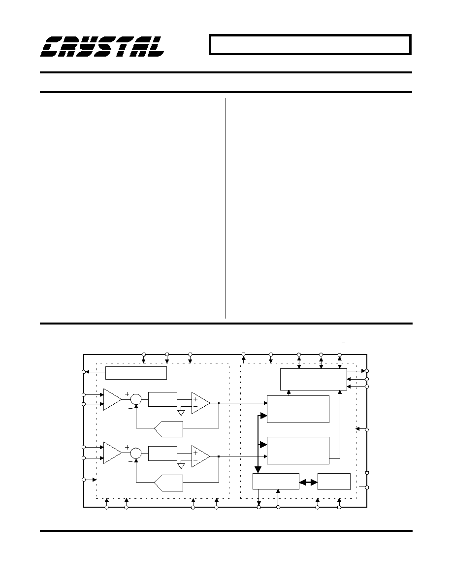
General Description
The CS5336, CS5338 & CS5339 are complete analog-
to-digital converters for stereo digital audio systems.
They perform sampling, analog-to-digital conversion and
anti-aliasing filtering, generating 16-bit values for both
left and right inputs in serial form. The output word rate
can be up to 50 kHz per channel.
The ADCs use delta-sigma modulation with 64X over-
sampling, followed by digital filtering and decimation,
which removes the need for an external anti-alias filter.
The CS5336 & CS5338 have an SCLK which clocks out
data on rising edges. The CS5339 has an SCLK which
clocks out data on falling edges.
The CS5336 has a filter passband of dc to 22kHz. The
CS5338 & CS5339 have a filter passband of dc to 24
kHz. The filters have linear phase, 0.01 dB passband
ripple, and >80 dB stopband rejection.
The ADC's are housed in a 0.6" wide 28-pin plastic DIP,
and also in a 0.3" wide 28-pin SOIC surface mount
package. Extended temperature range versions of the
CS5336 are also available.
ORDERING INFORMATION: See Page 3-59
Crystal Semiconductor Corporation
P.O. Box 17847, Austin, TX 78760
(512) 445-7222 FAX: (512) 445-7581
AUG '93
DS23F1
3-39
16-Bit, Stereo A/D Converters for Digital Audio
Semiconductor Corporation
A IN R
S /H
A G N D
D A C
A IN L
S /H
D A C
S e ria l O u tp u t In te rfa ce
V o ltag e R e fe re n ce
V R E F
C a lib ra tio n
S R A M
C o m p ara to r
C o m p ara to r
L P F ilte r
L P F ilte r
Z E R O L
Z E R O R
27
26
2
3
1
28
V D +
18
D G N D
19
1 7
V A -
5
V L +
25
V A +
4
S M O D E
13
N C
22
N C
8
T S T
11
S C L K
15
A P D
6
A C A L
7
IC L K A
23
D P D
10
D C A L
9
L G N D
24
D ig ita l D e cim a tio n
Filter
D ig ita l D e cim a tio n
Filter
C a lib ra tio n
Microcontroller
L /R
14
F S Y N C
S D A T A
16
C M O D E
12
IC L K D
20
O C L K D
21
CS5336 CS5338 CS5339
CS5336,8,9-K
CS5336-B
CS5336-T
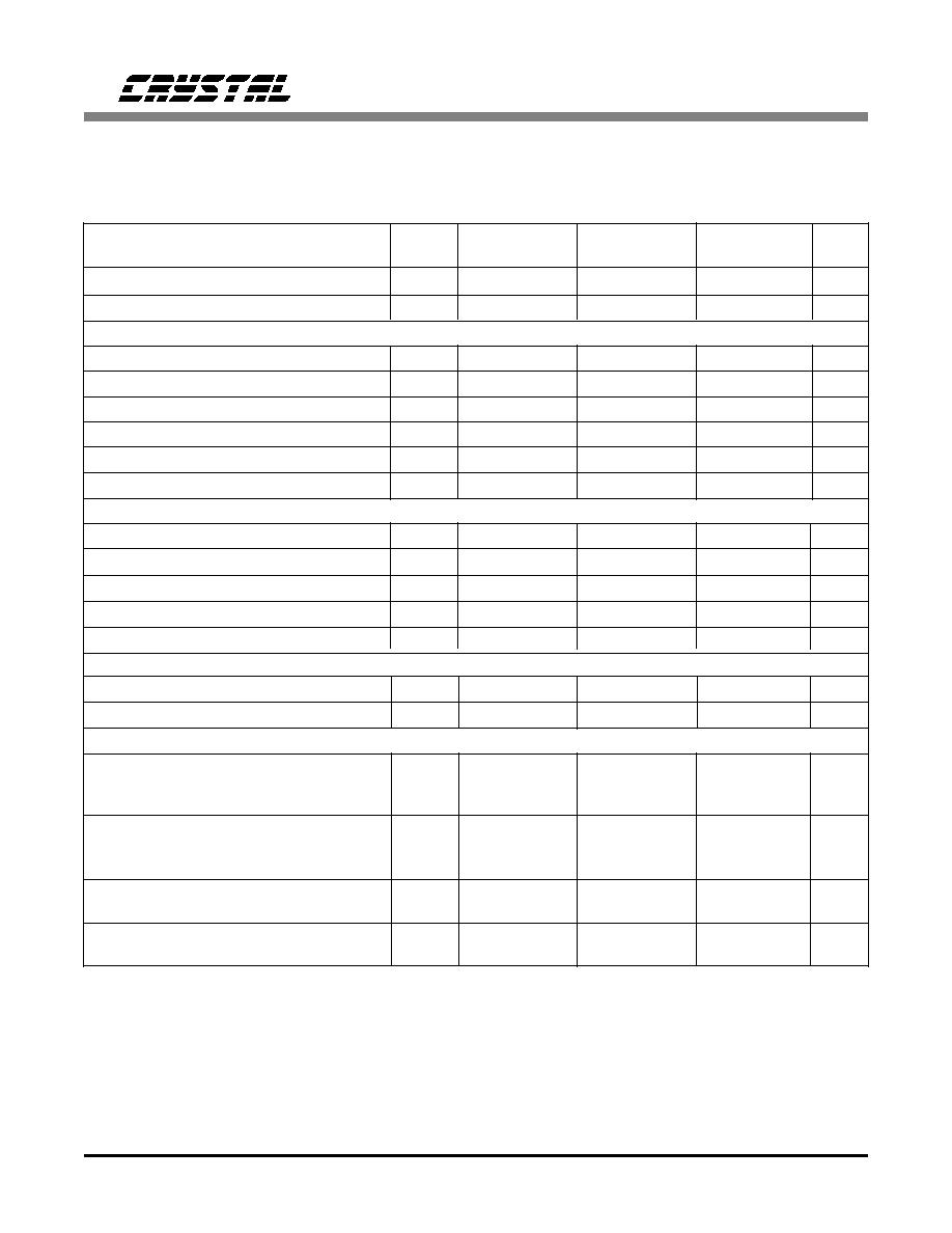
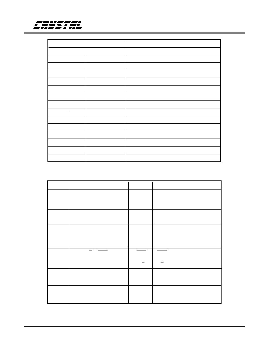
Parameter
Symbol Min Typ Max Min Typ Max Min Typ Max Units
Specified Temperature Range
T
A
0
to
70
-40
to
+85
-55
to
+125
∞
C
Resolution
16
-
-
16
-
-
16
-
-
Bits
Dynamic Performance
Dynamic Range
92.7 95.7
-
90
93.5
-
84
92
-
dB
Signal-to-(Noise + Distortion); THD+N
S/(N+D) 90.7 92.7
-
85
89
-
82
86
-
dB
Signal to Peak Noise
-
96
-
-
95
-
-
94
-
dB
Total Harmonic Distortion
THD
.0025 .001
-
.005 .001
-
.013 .005
-
%
Interchannel Phase Deviation
-
.0001
-
-
.0001
-
-
.0001
-
∞
Interchannel Isolation
(dc to 20 kHz)
100 106
-
90
106
-
83
96
-
dB
dc Accuracy
Interchannel Gain Mismatch
-
0.01 0.05
-
.01
.05
-
.01
0.1
dB
Gain Error
(includes Vref tolerance)
-
±
1
±
5
-
±
2
±
5
-
±
3
±
6
%
Gain Drift
(includes Vref drift, Note 1)
-
25
-
-
70
-
-
70
-
ppm/
∞
C
Bipolar Offset Error
(Note 2)
-
±
5
±
15
-
±
10
±
30
-
±
16
±
65
LSB
Offset Drift
(Note1)
-
15
-
-
20
-
-
20
-
ppm/
∞
C
ANALOG CHARACTERISTICS
(Logic 0 = GND; Logic 1 = VD+; K grade: T
A
= 25
∞
C; B and T
grades: T
A
= T
MIN
to T
MAX
; VA+, VL+,VD+ = 5V; VA- = -5V; Full-Scale Input Sinewave, 1kHz; Output word
rate = 48 kHz; SCLK = 3.072 MHz; Source Impedance = 50
with 10 nF to AGND; Measurement Bandwidth is
10 Hz to 20 kHz; unless otherwise specified.)
Analog Input
Input Voltage Range
(
±
Full Scale)
VIN
±
3.5
±
3.68
-
±
-3.5
±
3.68
-
±
3.5
±
3.68
-
V
Input Impedance
ZIN
-
65
-
-
65
-
-
65
-
k
Power Supplies
Power Supply Current
(VA+)+(VL+)
IA+
-
25
35
-
25
35
-
25
35
mA
with APD, DPD low
VA-
IA-
-
-25
-35
-
-25
-35
-
-25
-35
mA
(Normal Operation)
VD+
ID+
-
30
45
-
30
45
-
30
50
mA
Power Supply Current
(VA+)+(VL+)
IA+
-
10
50
-
10
50
-
10
50
µ
A
with APD, DPD high
VA-
IA-
-
-10
-50
-
-10
-50
-
-10
-50
µ
A
(Power-Down Mode)
VD+
ID+
-
10
400
-
10
400
-
10
400
µ
A
Power Consumption
(APD, DPD Low)
PDN
-
400 575
-
400 575
-
400 600
mW
(APD, DPD High)
PDS
-
0.15 2.5
-
0.15 2.5
-
0.15 2.5
mW
Power Supply
(dc to 26 kHz)
PSRR
-
54
-
-
54
-
-
54
-
dB
Rejection Ratio
(26 kHz to 3.046 MHz)
-
100
-
-
100
-
-
100
-
dB
Notes: 1. This parameter is guaranteed by design and/or characterization.
2. After calibration with DCAL connected to ACAL, and ZEROL & ZEROR terminated to AGND with an
impedance matched to the AINR & AINL source impedance. Executing a calibration with ACAL tied
low (See Power Down and Offset Calibration section) will yield an offset error of typically less than
±
5LSB.
Specifications are subject to change without notice.
CS5336, CS5338, CS5339
3-40
DS23F1

Units
Typ
Min
Symbol
Parameter
Max
V
V
-
-
-
VOH
V OL
High-Level Output Voltage at Io = -20uA
Low-Level Output Voltage at Io = 20uA
-
0.1
uA
1.0
-
Iin
Input Leakage Current
V
V
-
-
70%VD+
-
VIL
VIH
Low-Level Input Voltage
High-Level Input Voltage
-
30% VD+
4.4
-
DIGITAL FILTER CHARACTERISTICS
(T
A
= 25
∞
C; VA+, VL+ ,VD+ = 5V
±
5%; VA- = -5V
±
5%; Output word rate of 48 kHz)
DIGITAL CHARACTERISTICS
(T
A
= 25
∞
C; VA+, VL+ ,VD+ = 5V
±
5%; VA- = -5V
±
5%)
Parameter
Units
Typ
Symbol
Min
Max
Passband Ripple
0.01
dB
Passband
kHz
kHz
Stopband
CS5336
CS5338, CS5339
26
3046
28
3044
kHz
kHz
Stopband Attenuation
80
dB
(Note 3)
Group Delay (OWR = Output Word Rate)
18/OWR
s
Group Delay Variation vs. Frequency
0.0
us
t gd
t gd
0
22
kHz
0
24
kHz
CS5336
CS5338, CS5339
(-3 dB)
(-3 dB)
0
20
0
22
CS5336
CS5338, CS5339
(-0.01 dB)
(-0.01 dB)
to
to
to
to
-
-
to
to
-
-
-
-
-
-
+
_
Notes:
3. The analog modulator samples the input at 3.072MHz for an output word rate of 48 kHz. There is
no rejection of input signals which are multiples of the sampling frequency (that is: there is
no rejection for n x 3.072MHz
±
22kHz for the CS5338 & CS5339, or n x 3.072MHz
±
20.0kHz for the
CS5336, where n = 0,1,2,3...).
ABSOLUTE MAXIMUM RATINGS
(AGND, LGND, DGND = 0V, all voltages with respect to GND)
Parameter
Input Current, Any Pin Except Supplies
DC Power Supplies:
Analog Input Voltage (AIN and ZERO pins)
Digital Input Voltage
Storage Temperature
Ambient Temperature (power applied)
mA
Units
V
V
C
C
Positive Logic
V
Positive Digital
V
Negative Analog
Positive Analog
V
V
Min
-
(VA- )- 0.3
-0.3
-0.3
+0.3
-0.3
-0.3
-55
-65
Symbol
I
in
V
INA
V
IND
T
A
T
stg
VL+
VD+
VA+
VA-
Max
+150
+125
(VA+ )+ 0.3
(VD+) + 0.3
(VA+) + 0.3
+6.0
-6.0
+6.0
+
_ 10
WARNING: Operation at or beyond these limits may result in permanent damage to the device.
Normal operation is not guaranteed at these extremes.
CS5336, CS5338, CS5339
DS23F1
3-41

Parameter
Symbol
Min
Typ
Max
Unit
ICLKD Period (CMODE low)
(Note 6)
t clkw1
78
-
3906
ns
ICLKD Low (CMODE low)
t clkl1
31
-
-
ns
ICLKD High (CMODE low)
t clkh1
31
-
-
ns
ICLKD rising to OCLKD rising (CMODE low)
t io1
5
-
40
ns
ICLKD Period (CMODE high)
t clkw2
52
-
2604
ns
ICLKD Low (CMODE high)
t clkl2
20
-
-
ns
ICLKD High (CMODE high)
t clkh2
20
-
-
ns
ICLKD rising or falling to OCLKD rising (CMODE high, Note 4)
t io2
5
-
45
ns
ICLKD rising to L/R edge (CMODE low, MASTER mode)
t ilr1
5
-
50
ns
ICLKD rising to FSYNC edge (CMODE low, MASTER mode)
t ifs1
5
-
50
ns
ICLKD rising to SCLK edge (CMODE low, MASTER mode)
t isclk1
5
-
50
ns
ICLKD falling to L/R edge (CMODE high, MASTER mode)
t ilr2
5
-
50
ns
ICLKD falling to FSYNC edge (CMODE high, MASTER mode)
t ifs2
5
-
50
ns
ICLKD falling to SCLK edge (CMODE high, MASTER mode)
t isclk2
5
-
50
ns
SCLK rising to SDATA valid (MASTER mode, Note 5)
t sdo
0
-
50
ns
SCLK duty cycle (MASTER mode)
40
50
60
%
SCLK rising to L/R (MASTER mode, Note 5)
t mslr
-20
-
20
ns
SCLK rising to FSYNC (MASTER mode, Note 5)
t msfs
-20
-
20
ns
SCLK Period (SLAVE mode)
t sclkw
155
-
-
ns
SCLK Pulse Width Low (SLAVE mode)
t sclkl
60
-
-
ns
SCLK Pulse Width High (SLAVE mode)
t sclkh
60
-
-
ns
SCLK rising to SDATA valid (SLAVE mode, Note 5)
t dss
-
-
50
ns
L/R edge to MSB valid (SLAVE mode)
t lrdss
-
-
50
ns
Falling SCLK to L/R edge delay (SLAVE mode, Note 5)
t slr1
30
-
-
ns
L/R edge to falling SCLK setup time (SLAVE mode, Note 5)
t slr2
30
-
-
ns
Falling SCLK to rising FSYNC delay (SLAVE mode, Note 5)
t sfs1
30
-
-
ns
Rising FSYNC to falling SCLK setup time (SLAVE mode, Note 5)
t sfs2
30
-
-
ns
DPD pulse width
t pdw
2 x tclkw
-
-
ns
DPD rising to DCAL rising
t pcr
-
-
50
ns
DPD falling to DCAL falling (OWR = Output Word Rate)
t pcf
-
4096
-
1/OWR
SWITCHING CHARACTERISTICS
(T
A
= 25
∞
C; VA+, VL+, VD+ = 5V
±
5%; VA- = -5V
±
5%; Inputs: Logic 0 = 0V, Logic 1 = VD+; C
L
= 20 pF)
Notes:
4. ICLKD rising or falling depends on DPD to L/R timing (see Figure 2).
5. SCLK is shown for CS5336, CS5338. SCLK is inverted for CS5339.
6. Specifies minimum output word rate (OWR) of 1 kHz.
CS5336, CS5338, CS5339
3-42
DS23F1
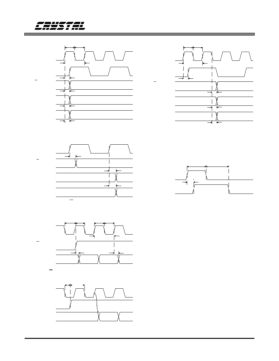
ICLKD
clkh
t
clkl
t
t
clkw1
OCLKD
(CMODE low)
t
io1
SDATA
SCLK input
(SLAVE mode)
(SLAVE mode)
L/R input
SCLK input
(SLAVE mode)
FSYNC input
(SLAVE mode)
SDATA
t
ilr1
FSYNC output
t
ifs1
SCLK output
t
isclk1
(MASTER mode)
L/R output
(MASTER mode)
(MASTER mode)
SCLK output
(MASTER mode)
t
mslr
SDATA
t
sdo
t
msfs
sclkl
t
dss
t
MSB
MSB-1
MSB-2
lrdss
t
sclkh
t
slr1
t
slr2
t
t
sclkw
MSB
MSB-1
MSB-2
sfs1
t
sfs2
t
L/ R output
(MASTER mode)
FSYNC output
(MASTER mode)
ICLKD
clkh2
t
clkl2
t
t
clkw2
t
ilr2
t
ifs2
t
isclk2
DPD
t
io2
OCLKD
(CMODE high)
FSYNC output
SCLK output
(MASTER mode)
L/R output
(MASTER mode)
(MASTER mode)
DCAL
pdw
t
pcr
t
pcf
t
ICLKD to Outputs Propagation Delays (CMODE low)
SCLK to SDATA, L/R & FSYNC - MASTER Mode
SCLK to L/R & SDATA - SLAVE mode, FSYNC high
FSYNC to SCLK - SLAVE Mode, FSYNC Controlled.
Power Down & Calibration Timing
ICLKD to Outputs Propagation Delays (CMODE high)
CS5336, CS5338, CS5339
DS23F1
3-43
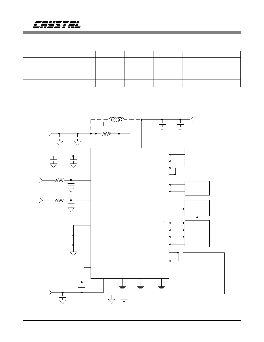
Audio
Data
Processor
CS5336
VREF
AINL
AINR
ZEROL
ZEROR
AGND
NC
NC
VA+
VA-
VL+
VD+
APD
DPD
ACAL
DCAL
TST
LGND
DGND
28
2
27
3
26
1
8
22
5
24
19
6
10
7
9
11
4
25
18
+5V Analog
0.1
µ
F
+
1
µ
F
0.1
µ
F
Control
0.1
µ
F
1
µ
F
-5V Analog
10 nF
10 nF
0.1
µ
F
Left Analog Input
Right Analog Input
A/D CONVERTER
10
µ
F
+
0.1
µ
F
1
µ
F
+
+
Ferrite Bead
51
51
51
VA+
SCLK
14
15
L/R
SDATA
16
CS5338
CS5339
Ferrite bead may
be used if VD+ is
+5V Digital
Power Down
& Calibrate
Mode
Settings
SMODE
CMODE
13
12
Timing
Logic
FSYNC
17
& Clock
ICLKD
20
21
23
OCLKD
ICLKA
derived from VA+.
An example ferrite
bead is Permag
VK200-2.5/52
If used, do not drive
any other logic
from VD+.
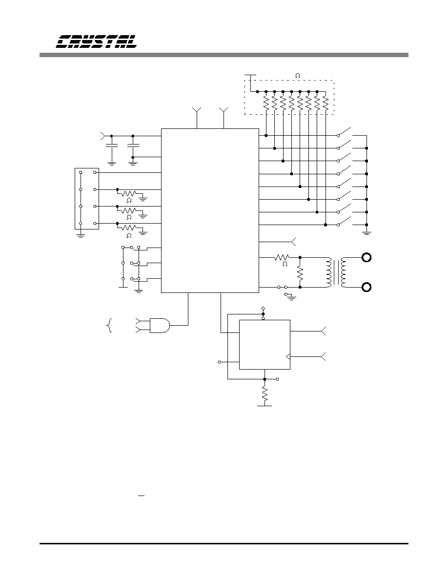
Figure 1. Typical Connection Diagram
RECOMMENDED OPERATING CONDITIONS
(AGND, LGND, DGND = 0V; all voltages with respect to ground)
DC Power Supplies:
V
Parameter
Symbol
Min
Typ
Max
Units
Positive Digital
Positive Logic
Positive Analog
Negative Analog
V
V
V
VD+
VL+
VA+
VA-
4.75
4.75
Analog Input Voltage
3.68
3.68
-
V
V AIN
4.75
4.75
_
5.0
5.0
5.0
5.0
_
5.25
5.25
_
VA+
_
(Note 7)
VA+
Notes:
7. The ADCs accept input voltages up to the analog supplies (VA+, VA-). They will produce a positive
full-scale output for inputs above 3.68 V and negative full-scale output for inputs below -3.68 V. These
values are subject to the gain error tolerance specification. Additional tag bits are output to indicate
the amount of overdrive.
CS5336, CS5338, CS5339
3-44
DS23F1

GENERAL DESCRIPTION
The CS5336, CS5338, and CS5339 are 16-bit, 2-
channel A/D converters designed specifically for
stereo digital audio applications. The devices use
two one-bit delta-sigma modulators which simul-
taneously sample the analog input signals at a 64
X sampling rate. The resulting serial bit streams
are digitally filtered, yielding pairs of 16-bit val-
ues. This technique yields nearly ideal conversion
performance independent of input frequency and
amplitude. The converters do not require difficult-
to-design or expensive anti-alias filters, and do not
require external sample-and-hold amplifiers or a
voltage reference.
An on-chip voltage reference provides for an in-
put signal range of
±
3.68 volts. Any zero offset is
internally calibrated out during a power-up self-
calibration cycle. Output data is available in serial
form, coded as 2's complement 16-bit numbers.
Typical power consumption of only 400 mW can
be further reduced by use of the power-down
mode.
For more information on delta-sigma modulation
and the particular implementation inside these
ADCs, see the references at the end of this data
sheet.
SYSTEM DESIGN
Very few external components are required to sup-
port the ADC. Normal power supply decoupling
components, voltage reference bypass capacitors
and a single resistor and capacitor on each input
for anti-aliasing are all that's required, as shown
in Figure 1.
Master Clock Input
The master input clock (ICLKD) into the ADC
runs the digital filter, and is used to generate the
modulator sampling clock. ICLKD frequency is
determined by the desired Output Word Rate
(OWR) and the setting of the CMODE pin.
CMODE high will set the required ICLKD fre-
quency to 384 X OWR, while CMODE low will
set the required ICLKD frequency to 256 X
OWR. Table 1 shows some common clock fre-
quencies. The digital output clock (OCLKD) is
always equal to 128 X OWR, which is always
2 X the input sample rate. OCLKD should be
connected to ICLKA, which controls the input
sample rate.
The phase alignment between ICLKD and
OCLKD is determined as follows: when CMODE is
OCLKD/
L/R
CMODE
ICLKD
ICLKA
SCLK
(kHz)
(MHz)
(MHz)
(MHz)
32
low
8.192
4.096
2.048
32
high
12.288
4.096
2.048
44.1
low
11.2896
5.6448
2.8224
44.1
high
16.9344
5.6448
2.8224
48
low
12.288
6.144
3.072
48
high
18.432
6.144
3.072
Table 1. Common Clock Frequencies
Figure 2. ICLKD to OCLKD Timing with CMODE
high (384 X OWR)
*
0
1
2
3
4
5
6
7
**
***
1
2
1
2
Input
L/ R
_
Input
DPD
Output
OCLKD
Input
L/ R
_
Output
OCLKD
Input
ICLKD
* DPD low is recognized on the next ICLKD rising edge (#0)
** L/R rising before ICLKD rising #2 causes OCLKD -1
*** L/R rising after ICLKD rising #2 causes OCLKD - 2
CS5336, CS5338, CS5339
DS23F1
3-45

low, ICLKD is divided by 2 to generate OCLKD.
The phase relationship between ICLKD and
OCLKD is always the same, and is shown in the
Switching Characteristics Timing Diagrams.
When CMODE is high, OCLKD is ICLKD di-
vided by 3. There are two possible phase
relationships between ICLKD and OCLKD,
which depend on the start-up timing between
DPD and L/R, shown in Figure 2.
Serial Data Interface
The serial data output interface has 3 possible
modes of operation: MASTER mode, SLAVE
mode with FSYNC high, and SLAVE mode with
FSYNC controlled. In MASTER mode, the A/D
converter is driven from a master clock (ICLKD)
and outputs all other clocks, derived from ICLKD
(see Figure 3). Notice the one SCLK cycle delay
between L/R edges and FSYNC rising edges.
FSYNC brackets the 16 data bits for each chan-
nel.
In SLAVE mode, L/R and SCLK are inputs. L/R
must be externally derived from ICLKD, and
should be equal to the Output Word Rate. SCLK
should be equal to the input sample rate, which is
equal to OCLKD/2. Other SCLK frequencies are
possible, but may degrade dynamic range because
of interference effects. Data bits are clocked out
via the SDATA pin using the SCLK and L/R in-
puts. The rising edge of SCLK causes the ADC to
Output
0
1
2
3
16 17 18 19 20 21
31
0
1
2
3
16 17 18 19 20 21
31
0
1
Output
Left Audio Data
Tag Bits
Left Data Tag
Right Audio Data
Tag Bits
Right Data Tag
*
SCLK for CS5336/8.
SCLK inverted for
CS5339
FSYNC
Output
15 14
1
0
T2 T1 T0
15 14
1
0
T2 T1 T0
SDATA
Output
SCLK
*
L/ R
Figure 3. Data Output Timing - MASTER mode
Figure 4. Data Output Timing - SLAVE Mode, FSYNC high
Input
0
1
2
16 17 18 19 20
31
0
1
2
16 17 18 19 20 21
31
0
1
Input
FSYNC
Input (high)
SCLK
*
L/ R
Left Audio Data
Tag Bits
Left Data Tag
Right Audio Data
Tag Bits
Right Data Tag
15 14
1
0
T2 T1 T0
15 14
1
0
T2 T1 T0
SDATA
Output
*
SCLK for CS5336/8.
SCLK inverted for
CS5339
15
15
30
CS5336, CS5338, CS5339
3-46
DS23F1

output each bit, except the MSB, which is clocked
out by the L/R edge. As shown in Figure 4, when
FSYNC is high, serial data bits are clocked imme-
diately following the L/R edge.
In SLAVE mode with FSYNC controlled, as
shown in Figure 5, when FSYNC is low, only the
MSB is clocked out after the L/R edge. With
FSYNC low, SCLK is ignored. When it is desired
to start clocking out data, bring FSYNC high
which enables SCLK to start clocking out data.
Bringing FSYNC low will stop the data being
clocked out. This feature is particularly useful to
position in time the data bits onto a common se-
rial bus.
The serial nature of the output data results in the
left and right data words being read at different
times. However, the words within an L/R cycle
represent simultaneously sampled analog inputs.
In all modes, additional bits are output after the
data bits: 3 tag bits and a left/right indicator. The
tag bits indicate a near-to-clipping input condition
for the data word to which the tag bits are at-
tached. Table 2 shows the relationship between
input level and the tag bit values. The serial bit
immediately following the tag bits is 0 for the
left channel, and 1 for the right channel. The re-
maining bits before the next L/R edge will be 1's
for the left channel and 0's for the right channel.
Normally, the tag bits are separated from the
audio data by the digital signal processor. How-
ever, if the tag bits are interpreted as audio data,
their position below the LSB would result as a
very small dc offset.
In all modes, SCLK is shown for the CS5336 and
CS5338, where data bits are clocked out on rising
edges. SCLK is inverted for the CS5339.
Input
0
1
2
Input
FSYNC
Input
SCLK
*
L/ R
Left Audio Data
Tag Bits
Left Data
Right Audio Data
Tag Bits
Right Data
16 17 18 19
20
0
1
2
16 17 18 19
20
15
15
SDATA
Output
15 14
1
0
T2 T1 T0
15
14
1
0
T2 T1 T0
15
15
Tag
Tag
**
**
***
***
*
***
**
Falling FSYNC stops SCLK from
clocking out SDATA
Rising FSYNC enables
SCLK to clock out SDATA
SCLK for CS5336/8.
SCLK inverted for CS5339
Figure 5. Data Output Timing - SLAVE Mode, FSYNC controlled
Table 2. Tag Bit Definition
Input Level
T2 T1 T0
1.375 x FS
1
1
1
1.250 x FS to 1.375 x FS
1
1
0
1.125 x FS to 1.250 x FS
1
0
1
1.000 x FS to 1.125 x FS
1
0
0
-1.006dB to 0.000dB
0
1
1
-3.060dB to -1.006dB
0
1
0
-6.000dB to -3.060dB
0
0
1
< -6.000dB
0
0
0
FS = Full Scale (0dB) Input
CS5336, CS5338, CS5339
DS23F1
3-47

Certain serial modes align well with various inter-
face requirements. A CS5339 in MASTER mode,
with an inverted L/R signal, generates I
2
S
(Philips) compatible timing. A CS5336 in MAS-
TER mode, using FSYNC, interfaces well with a
Motorola DSP56000. A CS5336 in SLAVE mode
emulates a CS5326 style interface, and also links
up to a DSP56000 in network mode.
Analog Connections
The analog inputs are presented to the modulators
via the AINR and AINL pins. The analog input
signal range is determined by the internal voltage
reference value, which is typically -3.68 volts.
The input signal range therefore is typically
± 3.68
volts.
The ADC samples the analog inputs at
3.072 MHz for a 12.288 MHz ICLKD (CMODE
low). For the CS5336, the digital filter rejects all
noise between 26 kHz and (3.072 MHz-26 kHz).
For the CS5338 and CS5339, the digital filter re-
jects all no ise between 28 kHz and
(3.072 MHz-28 kHz). However, the filter will not
reject frequencies right around 3.072 MHz (and
multiples of 3.072 MHz). Most audio signals do
not have significant energy at 3.072 MHz. Never-
theless, a 51
resistor in series with the analog
input, and a 10 nF NPO or COG capacitor to
ground will attenuate any noise energy at 3.072
MHz, in addition to providing the optimum
source impedance for the modulators. The use of
capacitors which have a large voltage coefficient
(such as general purpose ceramics) should be
avoided since these can degrade signal linearity. If
active circuitry precedes the ADC, it is recom-
mended that the above RC filter is placed between
the active circuitry and the AINR and AINL pins.
The above example frequencies scale linearly with
output word rate.
The on-chip voltage reference output is brought
out to the VREF pin. A 10
µ
F electrolytic capaci-
tor in parallel with a 0.1
µ
F ceramic capacitor
attached to this pin eliminates the effects of high
frequency noise. Note the negative value of VREF
when using polarized capacitors. No load current
may be taken from the VREF output pin.
The analog input level used as zero during the
offset calibration period (described later) is input
on the ZEROL and ZEROR pins. Typically, these
pins are directly attached to AGND. For the ulti-
mate in offset nulling, networks can be attached to
ZEROR and ZEROL whose impedances match
the impedances present on AINL and AINR.
Power-Down and Offset Calibration
The ADC has a power-down mode wherein typi-
cal consumption drops to 150
µ
W. In addition,
exiting the power-down state initiates an offset
calibration procedure.
APD and DPD are the analog and digital power-
down pins. When high, they place the analog and
digital sections in the power-down mode. Bring-
ing these pins low takes the part out of
power-down mode. DPD going low initiates a
calibration cycle. If not using the power down
feature, APD should be tied to AGND. When us-
ing the power down feature, DPD and APD may
be tied together if the capacitor on VREF is not
DCAL
DPD
Cal Period
(4096 x L/R clocks)
(85.33 ms @ 48kHz)
Filter Delay Time
(~40 L/R periods)
(~2 ms @ 48 kHz)
Normal Operation
Figure 6. Initial Calibration Cycle Timing
CS5336, CS5338, CS5339
3-48
DS23F1

greater than 10
µ
F, as stated in the "Power-Up
Considerations" section.
During the offset calibration cycle, the digital sec-
tion of the part measures and stores the value of
the calibration input of each channel in registers.
The calibration input value is subtracted from all
future outputs. The calibration input may be ob-
tained from either the analog input pins (AINL
and AINR) or the zero pins (ZEROL and
ZEROR) depending on the state of the ACAL pin.
With ACAL low, the analog input pin voltages are
measured, and with ACAL high, the zero pin volt-
ages are measured.
As shown in Figure 6, the DCAL output is high
during calibration, which takes 4096 L/R clock
cycles. If DCAL is connected to the ACAL input,
the calibration routine will measure the voltage on
ZEROR and ZEROL. These should be connected
directly to ground or through a network matched
to that present on the analog input pins. Internal
offsets of each channel will thus be measured and
subsequently subtracted.
Alternatively, ACAL may be permanently con-
nected low and DCAL utilized to control a
multiplexer which grounds the user's front end.
In this case, the calibration routine will measure
and store not only the internal offsets but also
any offsets present in the front end input circuitry.
During calibration, the digital output of both
channels is forced to a 2's complement zero. Sub-
traction of the calibration input from conversions
after calibration substantially reduces any
power on click that might otherwise be experi-
enced. A short delay of approximately 40 output
words will occur following calibration for the
digital filter to begin accurately tracking audio
band signals.
Power-up Considerations
Upon initial application of power to the supply
pins, the data in the calibration registers will be
indeterminate. A calibration cycle should always
be initiated after application of power to replace
potentially large values of data in these registers
with the correct values.
The modulators settle very quickly (a matter of
microseconds) after the analog section is powered
on, either through the application of power, or by
exiting the power-down mode. The voltage refer-
ence can take a much longer time to reach a final
value due to the presence of large external capaci-
tance on the VREF pin; allow approximately
5 ms/
µ
F. The calibration period is long enough to
allow the reference to settle for capacitor values of
up to 10
µ
F. If a larger capacitor is used, addi-
tional time between APD going low and DPD
going low should be allowed for VREF settling
before a calibration cycle is initiated.
Grounding and Power Supply Decoupling
As with any high resolution converter, the ADC
requires careful attention to power supply and
grounding arrangements if its potential perform-
ance is to be realized. Figure 1 shows the
recommended power arrangements, with VA+,
VA- and VL+ connected to a clean
±
5 V supply.
VD+, which powers the digital filter, may be run
from the system +5V logic supply, provided that
it is not excessively noisy (<
±
50 mV pk-to-pk).
Alternatively, VD+ may be powered from VA+ via
a ferrite bead. In this case, no additional devices
should be powered from VD+. Analog ground and
digital ground should be connected together near
to where the supplies are brought onto the printed
circuit board. Decoupling capacitors should be as
near to the ADC as possible, with the low value
ceramic capacitor being the nearest.
The printed circuit board layout should have sepa-
rate analog and digital regions and ground planes,
CS5336, CS5338, CS5339
DS23F1
3-49

with the ADC straddling the boundary. All sig-
nals, especially clocks, should be kept away from
the VREF pin in order to avoid unwanted cou-
pling into the modulators. The VREF decoupling
capacitors, particularly the 0.1
µ
F, must be posi-
tioned to minimize the electrical path from VREF
to Pin 1 AGND and to minimize the path between
VREF and the capacitors. An evaluation board is
available which demonstrates the optimum layout
and power supply arrangements, as well as allow-
ing fast evaluation of the ADC.
To minimize digital noise, connect the ADC digi-
tal outputs only to CMOS inputs.
Synchronization of Multiple CS5336/8/9
In systems where multiple ADC's are required,
care must be taken to insure that the ADC internal
clocks are synchronized between converters to in-
sure simultaneous sampling. In the absence of this
synchronization, the sampling difference could be
one ICLKD period which is typically 81.4 nsec
for a 48 kHz sample rate.
SLAVE MODE
Synchronous sampling in the slave mode is
achieved by connecting all DPD and APD pins to
a single control signal and supplying the same
ICLKD and L/R to all converters.
MASTER MODE
The internal counters of the CS5336/8/9 are reset
during DPD/APD high and will start simultane-
ously by insuring that the release of DPD/APD
for all converters is internally latched on the same
rising edge of ICLKD. This can be achieved by
connecting all DPD/APD pins to the same
control signal and insuring that the DPD/APD
falling edge occurs outside a
±
30 ns window
either side of an ICLKD rising edge.
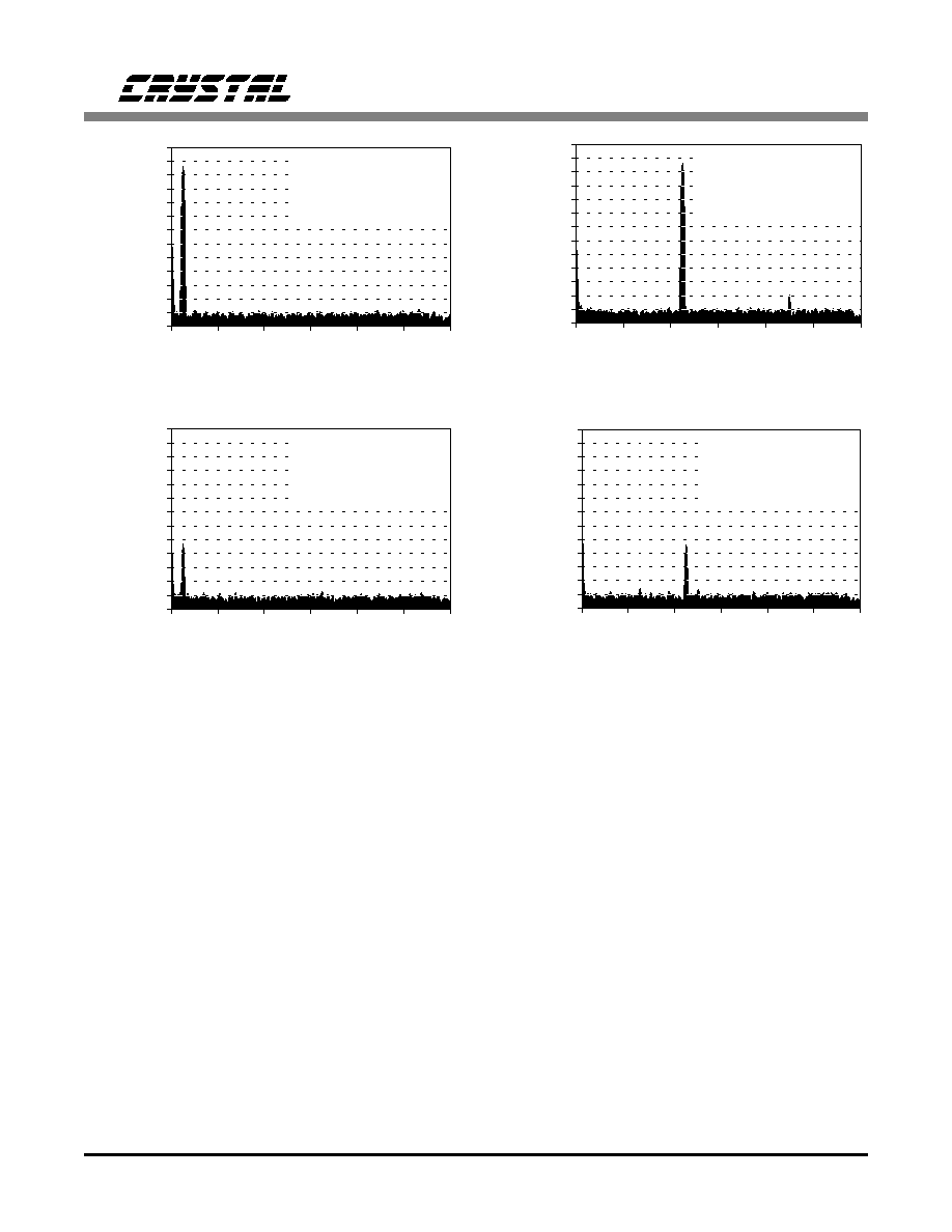
PERFORMANCE
FFT Tests
For FFT based tests, a very pure sine wave is pre-
sented to the ADC, and an FFT analysis is
performed on the output data. The resulting spec-
trum is a measure of the performance of the ADC.
Figure 7 shows the spectral purity of the CS5336
with a 1 kHz, -10 dB input. Notice the low noise
floor, the absence of any harmonic distortion, and
the Dynamic Range value of 95.41 dB.
Figure 8 shows the CS5336 high frequency per-
formance. The input signal is a -10 dB, 9 kHz
sine wave. Notice the small 2nd harmonic at
110 dB down.
Figure 9 shows the low-level performance of the
CS5336. Notice the lack of any distortion compo-
nents. Traditional R-2R ladder based ADC's can
have problems with this test, since differential
non-linearities around the zero point become very
significant. Figure 10 shows the same very low
input amplitude performance, but at 9kHz input
frequency.
CS5336, CS5338, CS5339
3-50
DS23F1
DNL Tests
A Differential Non-Linearity test is also shown.
Here, the converter is presented with a linear ramp
signal. The resulting output codes are counted to
yield a number which is proportional to the
codewidth. A plot of codewidth versus code
graphically illustrates the uniformity of the
codewidths. Figure 11 shows the excellent Differ-
ential Non-Linearity of the CS5336. This plot
displays the worst case positive and negative er-
rors in each of 512 groups of 128 codes.
Codewidths typically are within
±
0.2 LSB's of
ideal. A delta-sigma modulator based ADC has no
inherent mechanism for generating DNL errors.
The residual small deviations shown in Figure 11
are a result of noise. Nevertheless, the perform-
ance shown is extremely good, and is superior to
typical R-2R ladder based designs.
Figure 10. CS5336 FFT Plot with -80 dB, 9 kHz Input
Figure 8. CS5336 FFT Plot with -10 dB, 9 kHz Input
Figure 7. CS5336 FFT Plot with -10 dB, 1 kHz Input
0
4
8
12
16
20
24
Input Frequency (kHz)
-130
-120
-110
-100
-90
-80
-70
-60
-50
-40
-30
-20
-10
0
Signal
Amplitude
Relative to
Full Scale
(dB)
Output Word Rate: 48 kHz
Full Scale: 7.3 Vp-p
S/(N+D): 85.41 dB
Dynamic Range: 95.41 dB
(dc to 20 kHz)
Figure 9. CS5336 FFT Plot with -80 dB, 1 kHz Input
0
4
8
12
16
20
24
Input Frequency (kHz)
-130
-120
-110
-100
-90
-80
-70
-60
-50
-40
-30
-20
-10
0
Signal
Amplitude
Relative to
Full Scale
(dB)
Output Word Rate: 48 kHz
Full Scale: 7.3 Vp-p
S/(N+D): 16.09 dB
Dynamic Range: 96.09 dB
(dc to 20 kHz)
0
4
8
12
16
20
24
Input Frequency (kHz)
-130
-120
-110
-100
-90
-80
-70
-60
-50
-40
-30
-20
-10
0
Signal
Amplitude
Relative to
Full Scale
(dB)
Output Word Rate: 48 kHz
Full Scale: 7.3 Vp-p
S/(N+D): 15.72 dB
Dynamic Range: 95.72 dB
(dc to 20 kHz)
0
4
8
12
16
20
24
Input Frequency (kHz)
-130
-120
-110
-100
-90
-80
-70
-60
-50
-40
-30
-20
-10
0
Signal
Amplitude
Relative to
Full Scale
(dB)
Output Word Rate: 48 kHz
Full Scale: 7.3 Vp-p
S/(N+D): 85.03 dB
Dynamic Range: 95.033 dB
(dc to 20 kHz)
CS5336, CS5338, CS5339
DS23F1
3-51
Digital Filter
Figures 12 through 17 show the performance of
the digital filter included in the ADC. All the plots
assume an output word rate of 48 kHz. The filter
frequency response will scale precisely with
changes in output word rate. The passband ripple
is flat to
±
0.01 dB maximum. Stopband rejection
is greater than 80 dB.
Figures 12,14 &16 show the CS5338 and CS5339
filter characteristics. Figure 17 is an expanded
view of the transition band.
Figures 13,15 & 17 show the CS5336 filter char-
acteristics. Figure 17 is an expanded view of the
transition band.
Figure 11. CS5336 Differential Non-Linearity Plot
0
65,535
Codes
32,768
DNL (LSB)
+1
0
-1
+1/2
-1/2
CS5336, CS5338, CS5339
3-52
DS23F1

20
21
22
23
24
25
26
27
28
Input Frequency (kHz)
Magnitude (dB)
-100
-90
-80
-70
-60
-50
-40
-30
-20
-10
0
22
23
24
25
26
27
28
29
30
Input Frequency (kHz)
-100
-90
-80
-70
-60
-50
-40
-30
-20
-10
0
Magnitude (dB)
Figure 16. CS5338/9 Digital Filter Transition Band
Figure 17. CS5336 Digital Filter Transition Band
0
4
8
12
16
20
24
Input Frequency (kHz)
-0.020
-0.010
0.000
0.010
0.020
Magnitude (dB)
0
8
16
24
32
40
48
Input Frequency (kHz)
-130
-120
-110
-100
-90
-80
-70
-60
-50
-40
-30
-20
-10
0
10
Magnitude (dB)
Figure 13. CS5336 Digital Filter Stopband Rejection
0
4
8
12
16
20
24
Input Frequency (kHz)
-0.020
-0.010
0.000
0.010
0.020
Magnitude (dB)
Figure 14. CS5338/9 Digital Filter Passband Ripple
0
8
16
24
32
40
48
Input Frequency (kHz)
-130
-120
-110
-100
-90
-80
-70
-60
-50
-40
-30
-20
-10
0
10
Magnitude (dB)
Figure 12. CS5338/9 Digital Filter Stopband Rejection
Figure 15. CS5336 Digital Filter Passband Ripple
CS5336, CS5338, CS5339
DS23F1
3-53

PIN DESCRIPTIONS
Power Supply Connections
VA+ - Positive Analog Power, PIN 4.
Positive analog supply. Nominally +5 volts.
VL+ - Positive Logic Power, PIN 25.
Positive logic supply for the analog section. Nominally +5 volts.
VA- - Negative Analog Power, PIN 5.
Negative analog supply. Nominally -5 volts.
AGND - Analog Ground, PIN 1.
Analog ground reference.
LGND - Logic Ground, PIN 24
Ground for the logic portions of the analog section.
VD+ - Positive Digital Power, PIN 18.
Positive supply for the digital section. Nominally +5 volts.
DGND - Digital Ground, PIN 19.
Digital ground for the digital section.
Analog Inputs
AINL, AINR - Left and Right Channel Analog Inputs, PINS 2, 27
Analog input connections for the left and right input channels. Nominally
±
3.68 volts full
scale.
ANALOG GROUND
AGND
VREF
VOLTAGE REFERENCE OUTPUT
LEFT CHANNEL ANALOG INPUT
AINL
AINR
RIGHT CHANNEL ANALOG INPUT
LEFT CHANNEL ZERO INPUT ZEROL
ZEROR RIGHT CHANNEL ZERO INPUT
POSITIVE ANALOG POWER
VA+
VL+
ANALOG SECTION LOGIC POWER
NEGATIVE ANALOG POWER
VA-
LGND
ANALOG SECTION LOGIC GROUND
ANALOG POWER DOWN INPUT
APD
ICLKA
ANALOG SECTION CLOCK INPUT
ANALOG CALIBRATE INPUT
ACAL
NC
NO CONNECT
NO CONNECT
NC
OCLKD DIGITAL SECTION OUTPUT CLOCK
DIGITAL CALIBRATE OUTPUT
DCAL
ICLKD
DIGITAL SECTION CLOCK INPUT
DIGITAL POWER DOWN INPUT
DPD
DGND
DIGITAL GROUND
TEST
TST
VD+
DIGITAL SECTION POSITIVE POWER
SELECT CLOCK MODE CMODE
FSYNC FRAME SYNC SIGNAL
SELECT SERIAL I/O MODE SMODE
SDATA SERIAL DATA OUTPUT
LEFT/RIGHT SELECT
L/R
SCLK
SERIAL DATA CLOCK
1
2
3
4
5
6
7
8
9
10
11
12
13
14
28
27
26
25
24
23
22
21
20
19
18
17
16
15
CS5336, CS5338, CS5339
3-54
DS23F1

ZEROL, ZEROR - Zero Level Inputs for Left and Right Channels, PINS 3, 26.
Analog zero level inputs for the left and right channels. The levels present on these pins
can be used as zero during the offset calibration cycle. Normally connected to AGND,
optionally through networks matched to the analog input networks.
Analog Outputs
VREF - Voltage Reference Output, PIN 28.
Nominally -3.68 volts. Normally connected to a 0.1
µ
F ceramic capacitor in parallel with a
10
µ
F or larger electrolytic capacitor. Note the negative output polarity.
Digital Inputs
ICLKA - Analog Section Input Clock, PIN 23.
This clock is internally divided by 2 to set the modulators' sample rate. Sampling rates,
output rates, and digital filter characteristics scale to ICLKA frequency. ICLKA frequency
is 128 X the output word rate. For example, 6.144 MHz ICLKA corresponds to an output
word rate of 48 kHz per channel. Normally connected to OCLKD.
ICLKD - Digital Section Input Clock, PIN 20.
This is the clock which runs the digital filter. ICLKD frequency is determined by the
required output word rate and by the CMODE pin. If CMODE is low, ICLKD frequency
should be 256 X the desired output word rate. If CMODE is high, ICLKD should be
384 X the desired output word rate. For example, with CMODE low, ICLKD should be
12.288 MHz for an output word rate of 48 kHz. This clock also generates OCLKD,
which is always 128 X the output word rate.
APD - Analog Power Down, PIN 6.
Analog section power-down command. When high, the analog circuitry is in power-down
mode. APD is normally connected to DPD when using the power down feature. If power
down is not used, then connect APD to AGND.
DPD - Digital Power Down, PIN 10
Digital section power-down command. Bringing DPD high puts the digital section into
power-down mode. Upon returning low, the ADC starts an offset calibration cycle. This
takes 4096 L/R periods (85.33 ms with a 12.288 MHz ICLKD). DCAL is high during the
calibrate cycle and goes low upon completion. DPD is normally connected to APD when
using the power down feature. A calibration cycle should always be initiated after
applying power to the supply pins.
ACAL - Analog Calibrate, PIN 7.
Analog section calibration command. When high, causes the left and right channel
modulator inputs to be internally connected to ZEROL and ZEROR inputs respectively.
May be connected to DCAL.
CS5336, CS5338, CS5339
DS23F1
3-55

CMODE - Clock Mode Select, PIN 12.
CMODE should be tied low to select an ICLKD frequency of 256 X the output word rate.
CMODE should be tied high to select an ICLKD frequency of 384 X the output word
rate.
SMODE - Serial Interface Mode Select, PIN 13.
SMODE should be tied high to select serial interface master mode, where SCLK, FSYNC
and L/R are all outputs, generated by internal dividers operating from ICLKD. SMODE
should be tied low to select serial interface slave mode, where SCLK, FSYNC and L/R
are all inputs. In slave mode, L/R, FSYNC and SCLK need to be derived from ICLKD
using external dividers.
Digital Outputs
SDATA - Serial Data Output, PIN 16.
Audio data bits are presented MSB first, in 2's complement format. Additional tag bits,
which indicate input overload and left/right channel data, are output immediately
following each audio data word.
DCAL - Digital Calibrate Output, PIN 9.
DCAL rises immediately upon entering the power-down state (DPD brought high). It
returns low 4096 L/R periods after leaving the power down state (DPD brought low),
indicating the end of the offset calibration cycle (which = 85.33 ms with a 12.288 MHz
ICLKD). May be connected to ACAL.
OCLKD - Digital Section Output Clock, PIN 21.
OCLKD is always 128 X the output word rate. Normally connected to ICLKA.
Digital Inputs or Outputs
SCLK - Serial Data Clock, PIN 15.
Data is clocked out on the rising edge of SCLK for the CS5336 and CS5338. Data is
clocked out on the falling edge of SCLK for the CS5339.
In master mode (SMODE high), SCLK is a continuous output clock at 64 X the output
word rate.
In slave mode (SMODE low), SCLK is an input, which requires a continuously supplied
clock at any frequency from 32 X to 128 X the output word rate (64 X is preferred).
When FSYNC is high, SCLK clocks out serial data, except for the MSB which appears on
SDATA when L/R changes.
CS5336, CS5338, CS5339
3-56
DS23F1

L/R - Left/Right Select, PIN 14.
In master mode (SMODE high), L/R is an output whose frequency is at the output word
rate. L/R edges occur 1 SCLK cycle before FSYNC rises. When L/R is high, left channel
data is on SDATA, except for the first SCLK cycle. When L/R is low, right channel data is
on SDATA, except for the first SCLK cycle. The MSB data bit appears on SDATA one
SCLK cycle after L/R changes.
In slave mode (SMODE low), L/R is an input which selects the left or right channel for
output on SDATA. The rising edge of L/R starts the MSB of the left channel data. L/R
frequency must be equal to the output word rate.
Although the outputs of each channel are transmitted at different times, the two words in
an L/R cycle represent simultaneously sampled analog inputs.
FSYNC - Frame Synchronization Signal, PIN 17.
In master mode (SMODE high), FSYNC is an output which goes high coincident with the
start of the first SDATA bit (MSB) and falls low immediately after the last SDATA audio
data bit (LSB).
In slave mode (SMODE low), FSYNC is an input which controls the clocking out of the
data bits on SDATA. FSYNC is normally tied high, which causes the data bits to be
clocked out immediately following L/R transitions. If it is desired to delay the data bits
from the L/R edge, then FSYNC must be low during the delay period. Bringing FSYNC
high will then enable the clocking out of the SDATA bits. Note that the MSB will be
clocked out based on the L/R edge, independent of the state of FSYNC.
Miscellaneous
NC - No Connection, PINS 8, 22.
These two pins are bonded out to test outputs. They must not be connected to any external
component or any length of PC trace.
TST -Test Input, PIN 11.
Allows access to the ADC test modes, which are reserved for factory use. Must be tied to
DGND.
CS5336, CS5338, CS5339
DS23F1
3-57

PARAMETER DEFINITIONS
Resolution - The total number of possible output codes is equal to 2
N,
where N = the number of bits
in the output word for each channel.
Dynamic Range - Full scale (RMS) signal to broadband noise ratio. The broadband noise is measured
over the specified bandwidth, and with an input signal 60dB below full-scale. Units in decibels.
Signal-to-(Noise plus Distortion) Ratio - The ratio of the rms value of the signal to the rms sum of all
other spectral components over the specified bandwidth (typically 10 Hz to 20 kHz), including
distortion components. Expressed in decibels.
Total Harmonic Distortion - The ratio of the rms sum of all harmonics up to 20 kHz to the rms value
of the signal. Units in percent.
Interchannel Phase Deviation - The difference between the left and right channel sampling times.
Interchannel Isolation - A measure of crosstalk between the left and right channels. Measured for
each channel at the converter's output with the input under test grounded and a full-scale signal
applied to the other channel. Units in decibels.
Interchannel Gain Mismatch - The gain difference between left and right channels. Units in
decibels.
Gain Error - The deviation of the measured full scale amplitude from the ideal full scale amplitude
value.
Gain Drift - The change in gain value with temperature. Units in ppm/
∞
C.
Bipolar Offset Error - The deviation of the mid-scale transition (111...111 to 000...000) from the ideal
(1/2 LSB below AGND). Units in LSBs.
CS5336, CS5338, CS5339
3-58
DS23F1

REFERENCES
1) "A Stereo 16-bit Delta-Sigma A/D Converter for Digital Audio" by D.R. Welland, B.P. Del Sig-
nore, E.J. Swanson, T. Tanaka, K. Hamashita, S. Hara, K. Takasuka. Paper presented at the 85th
Convention of the Audio Engineering Society, November 1988.
2) " The Effects of Sampling Clock Jitter on Nyquist Sampling Analog-to-Digital Converters, and on
Oversampling Delta Sigma ADC's" by Steven Harris. Paper presented at the 87th Convention of the
Audio Engineering Society, October 1989.
3) " An 18-Bit Dual-Channel Oversampling Delta-Sigma A/D Converter, with 19-Bit Mono Applica-
tion Example" by Clif Sanchez. Paper presented at the 87th Convention of the Audio Engineering
Society, October 1989.
Ordering Guide
Model
Resolution
Passband
SCLK
Temperature
Package
CS5336-KP
16-bits
22 kHz
active
0
∞
C to 70
∞
C
28-pin Plastic DIP
CS5336-BP
16-bits
22 kHz
active
-40 to +85
∞
C
28-pin Plastic DIP
CS5338-KP
16-bits
24 kHz
active
0
∞
C to 70
∞
C
28-pin Plastic DIP
CS5339-KP
16-bits
24 kHz
active
0
∞
C to 70
∞
C
28-pin Plastic DIP
CS5336-KS
16-bits
22 kHz
active
0
∞
C to 70
∞
C
28-pin SOIC
CS5336-BS
16-bits
22 kHz
active
-40 to +85
∞
C
28-pin SOIC
CS5338-KS
16-bits
24 kHz
active
0
∞
C to 70
∞
C
28-pin SOIC
CS5339-KS
16-bits
24 kHz
active
0
∞
C to 70
∞
C
28-pin SOIC
CS5336-TC
16-bits
22 kHz
active
-55 to +125
∞
C
28-pin Sidebrazed Ceramic DIP
CDB5336
CS5336 Evaluation Board
CDB5338
CS5338 Evaluation Board
CDB5339
CS5339 Evaluation Board
CS5336, CS5338, CS5339
DS23F1
3-59

Features
∑
∑
Demonstrates recommended layout
and grounding arrangements
∑
∑
CS8402 Generates AES/EBU, S/PDIF
& CP-340 Compatible Digital Audio
∑
∑
Buffered Serial Output Interface
∑
∑
16-Bit Parallel Output Interface
∑
∑
Digital and Analog Patch Areas
∑
∑
On-board or externally supplied system
timing
General Description
The CDB5336, CDB5338 & CDB5339 evaluation
boards allow fast evaluation of the CS5336, CS5338
and CS5339 16-bit, stereo A/D converters. The boards
generate all converter timing signals and provide both
parallel and serial output interfaces. Evaluation re-
quires a digital signal processor, a low-distortion signal
source, and a power supply.
Also included is a CS8402 digital audio transmitter I.C.,
which can generate AES/EBU, S/PDIF & EIAJ CP-340
compatible audio data.
The evaluation boards may also be configured to ac-
cept external timing signals for operation in a user
application during system development.
ORDERING INFORMATION:
CDB5336, CDB5338, CDB5339
Crystal Semiconductor Corporation
P.O. Box 17847, Austin, TX 78760
(512) 445 7222 FAX: (512) 445 7581
AUG '93
DS23DB5
3-60
Evaluation Board for CS5336, CS5338 & CS5339
Semiconductor Corporation
CDB5336
CDB5338 CDB5339
CS5336,
EXTCLKIN
AINR
A IN L
SDATA
SCLK
SERIAL TO
PARALLEL
CONVERTER
SERIAL
OUTPUT
DATA
PARALLEL
OUTPUT
DATA
L/R
ANALOG
PATCH
AREA
PATCH
AREA
DIGITAL
POWER SUPPLY
REGULATION &
CONDITIONING
NETWORK
OFFSET
CALIBRATION
+5V
GND
+15V
-15V
GND
CS5338,
OR
CS5339
Input
Buffer
Input
Buffer
CLOCK / TIMING
GENERATOR
FSYNC
A/D CONVERTER
CS8402
DIGITAL AUDIO
LINE DRIVER
DIGITAL
AUDIO
DATA

Power Supply Circuitry
The schematic diagram in Figure 1 shows the
evaluation board power supply circuitry. Power
is supplied to the evaluation board by five bind-
ing posts. The
±
5 Volt analog power supply
inputs of the converter are derived from
±
15
Volts using the voltage regulators U10 and U11.
The +5 Volt digital supply for the converter and
the discrete logic on the board is provided by the
+5V and DGND binding posts. D1, D2 and D4
are transient suppressors which also provide pro-
tection from incorrectly connected power supply
leads. C25-C28, C30 and C31 provide general
power supply filtering for the analog supplies.
As shown in Figure 2, C10-C13 provide local-
ized decoupling for the converter VA+ and VA-
pins. Note that C13 is connected between VA-
and VA+ and not VA- and AGND. Space for a
ferrite bead inductor, L1, has been provided so
that the board may be modified to power the
converter's VD+ input directly from the VA+
supply. Note that the trace connecting the VD+
power to the VD+ of the converter must be bro-
ken before L1 may be installed. R5 and C7 low-
pass filter the analog logic power supply pin,
VL+. The evaluation board uses both an analog
and a digital ground plane which are connected
at a single point by J1. This ground plane ar-
rangement isolates the board's digital logic from
the analog circuitry.
Offset Calibration & Reset Circuit
Figure 1, shows the optional offset calibration
circuit provided on the evaluation board. Upon
power-up, this circuit provides a pulse on the
Analog-to-Digital Converter's DPD pin initiating
an offset calibration cycle. Releasing SW1 also
initiates an offset calibration cycle. P6 (see Fig-
ure 2) selects the signal source used during
offset calibration. In the "AIN" position, the
AINL and AINR inputs are selected during cali-
bration, while in the "ZERO" position, the
ZEROL and ZEROR inputs are selected.
C25
C27
C26
C28
0.22 uF
0.47 uF
J1
+
C30
47 uF
C31
+
47 uF
0.22 uF
78L05
OUT
COM
U10
IN
D4
D2
0.47 uF
C9
+
C8
47 uF
0.1 uF
D1
+15V
-15V
+5V
U11
79L05
COM
IN
OUT
DGND
AGND
VA+
VA-
VD+
D1 = P6KE-6V8P from Thomson
D2 = D4 = 1N6276A 1.5KE
AGND
DGND
VD+
10k
C15
0.1uF
D3
1N4148
SW1
CAL
R26
Cal
(DPD CS5336)
10
11
U7D
RST
CS8402
8
9
U7E
Figure 1. Power Supply and Reset Circuitry
CDB5336,8,9
DS23DB5
3-61

CS5336
VA-
APD
DPD
ACAL
DCAL
5
6
7
9
VA+
AINR
27
ZEROL
3
ZEROR
26
AGND
1
VD+
VL+
4
0.1 uF
1 uF
VREF
28
+
0.1 uF
1 uF
+
0.1 uF
51
U1
1 uF
+
0.1 uF
NC
NC
8
22
TST
11
DGND
19
LGND
24
10 nF
51
AINL
2
10 nF
R4*
C4*
R3*
C3*
NPO
NPO
C1
C2
R1
R2
25
18
C5
C6
L1
C10
C11
C12
R5
C7
10
P6
AIN
ZERO
14
SDATA
16
Cal
SDATA
L/R
C13
VD+
VL+
VA+
DCAL
L/R
L/R
SDATA
VA-
VD+
VA+
VA-
0.1 uF
+
C17
C16
10 uF
Cal
CMODE
SMODE
R7
12
13
20 k
VD+
SCLK
15
SCLK
SCLK
FSYNC
17
FSYNC
FSYNC
ICLKD
Oscillator
Module
C15
0.1 uF
8
12.288 MHz
7
14
VD+
NC
1
P7
EXT
R6*
CLKIN
20
OCLKD
ICLKA
ICLKA
21
23
VD+
1
2
7
14
MCK
8402
3
C14
0.1 uF
U8A
ICLKD
EXT
INT
10 nF
10 nF
51
51
51
75
* Optional
U3
Pins 1,13
U9
From
Buffers
Fig 3
CS5338
CS5339
Figure 2 ADC Connections
CDB5336,8,9
3-62
DS23DB5

Analog Inputs
As shown in Figure 2, the analog input signals
are connected to the CS5336 via an RC network.
R1 and C1 provide antialiasing and optimum
source impedance for the right analog input
channel while R2 and C2 do so for the left chan-
nel. The ZEROR and ZEROL inputs are tied to
the analog ground plane on the board as shipped
from the factory, but space is provided for an op-
tional RC section on each. These RC sections
may be added to model the output impedance of
the analog signal source to minimize offset error
during calibration.
Figure 3 shows the optional input buffer circuit.
This can be used as an example input buffer cir-
cuit for your application. If the ADC is driven
from a 50
source impedance signal generator,
the input buffer amplifiers may be bypassed.
Place P8 and P9 jumpers in the OUT position,
and short circuit R1 and R2. This ensures that
the ADC is driven from a 50
source resis-
tance. Also remove U13 op-amp, to remove the
1k
load impedance.
Timing Generator
P7 selects the master clock source supplied to
the ICLKD pin of the converter. As shipped from
the factory, P7 is set to the "INT" position to
select the 12.288 MHz clock signal provided by
U3. An external master clock signal may be con-
nected to the EXTCLKIN connector and selected
by placing P7 in the "EXT" position. Note that
R6, tied between EXTCLKIN and GND, is
available for impedance matching an external
clock source. The board is shipped with SMODE
high, which selects MASTER timing mode. In
this mode, SCLK, L/R and FSYNC are all out-
puts, generated by the converter from ICLKD.
Serial Output Interface
The serial output interface is provided by the
S DATA , S C L K, F S YN C an d L /R B NC
connectors on the evaluation board. These out-
_
+
U13A
VA+
0.1 uF
8
1 k
R22
4
VA-
0.1 uF
1
2
3
1 k
R21
R1, Fig 2
U13B
1 k
R24
7
6
5
1 k
R23
R2, Fig 2
AINL
AINR
IN
OUT
IN
OUT
P9
P8
C32
C33
_
+
MC33078P
Figure 3. Input Buffer Circuit
CDB5336,8,9
DS23DB5
3-63
puts are buffered, as shown in Figure 5, in order
to isolate the converter from the digital signal
processor. If slave mode is selected by pulling
SMODE low, then U9 (74HC243) will change to
the opposite direction, and act as an input buffer.
U9 is provided to protect against inadvertent ex-
ternal driving of SCLK, L/R and FSYNC while
in MASTER mode. U9 is not necessary in your
application circuit.
Jumper P4 allows the board to be configured for
either the CS5336/38, or the CS5339, which
have opposite polarities of SCLK.
Parallel Output Interface
Figure 6 depicts the parallel output interface on
the evaluation board. 16-bit words are assembled
from the serial data output of the converter. Each
bit of serial data is clocked out of the converter
VD+
MCK
SCK
PRO
FSYNC
SDATA
GND
V
C
U
M0
M1
M2
CS8402
U2
C7/C3
C1/FC0
C6/C2
C9/C15
EM1/C8
EM0/C9
CRE/FC1
RST
TXP
TXN
CBL
U8D
VD+
1 4 2 5 6 7 8 9 3
10 k
SIP
2
1
3
4
12
13
14
24
RST
___
20
17
R20
2
4
1
3
R19
110
OCLKD P4
5
6
C24
0.1 uF
C34
1 uF
+
R18 20 k
R17
R16 20 k
20 k
Q2
Q2
RESET2
D2
CLK
SET2
13
9
12
11
10
8
+5 V
R11
47 k
__
L/R CS5336
FSYNC CS5336
7
74HC74
U12B
CS5336
FSYNC
SDATA
12
13
11
74HC08
21
22
23
9
10
11
15
18
19
8
____
__
__
__ ___
__ __
__
__ __
____
P3
CBL
V
C
U
16
3
2
4
5
6
8
7
1
14
15
13
12
11
9
10
16
_
Digital
Output
DIPSW 8
SW 2
VD+
PULSE PE65612
SCHOTT 67125450
VD+
Figure 4. CS8402 Digital Audio Line Driver Connections
CDB5336,8,9
3-64
DS23DB5

on the rising edge of SCLK and shifted into the
16-bit shift register formed by U4 and U5 on
SCLK's falling edge. After all data bits for the
selected channel have been shifted into U4 and
U5 the data is latched onto P1 by a delayed ver-
sion of FSYNC.
P5 selects the channel whose output data will be
converted to parallel form and presented on P1.
With P5 in the "B" (both) position, parallel data
from one channel will be presented first with
data from the other channel presented sub-
sequently. In the "L" (left) position, only left
channel conversions will be presented, while in
the "R" (right) position only right channel con-
versions are presented.
Two interface mechanisms are provided for read-
ing the data from this port. With the first, the
edges of L/R may be used to clock the parallel
data into the digital signal processor. (Set jumper
P2 into the L/R position.) Alternatively, a hand-
shake protocol implemented with DACK and
DRDY may be used to transfer data to the signal
processor. (Set jumper P2 to the DRDY posi-
tion.) The fall of DRDY informs the digital
signal processor that a new data word is avail-
able. The processor then reads the port and
acknowledges the transfer by asserting DACK.
Note that DRDY will not be asserted again un-
less DACK is momen tarily b ro ught high
although new data will continue to be latched
onto the port.
Digital Audio Standard Interface
Included on the evaluation board is a CS8402
Digital Audio Line Driver. This device can im-
plement AES/EBU, S/PDIF and EIAJ CP-340
interface standards. Figure 4 shows the sche-
matic for the CS8402. P3 allows the C, U and V
bits to be driven from external logic using the
CBL output for block synchronization. SW2 pro-
vides 8 DIP switches to select various modes
and bits for the CS8402. Table 3 lists the settings
for the professional mode which is the default
setting for the evaluation board from the factory.
The third switch selects between professional
U9
A-to-B
B-to-A
A4
B4
VCC
GND
B1
B2
B3
VD+
A1
A2
A3
SCLK
FSYNC
L/R
Enable
Enable
13
VD+
R8
20 k
SMODE
SCLK
FSYNC
SDATA
R9
20 k
R10
20 k
9
10
11
1
13
14
7
3
4
5
8
6
15
17
14
16
9
10
8
U8C
VD+
SDATA
SDATA
SDATA
L/R
L/R
FSYNC
SCLK
74HC08
74HC243
0.1 uF
C20
U8B
4
5
6
5336/38
5337/39
3
4
U7B
Pin 11
U4, U5
595's
CS8402
Pin 6
P4
Figure 5. Serial Output Interface
CDB5336,8,9
DS23DB5
3-65

D15
D14
D13
D12
D11
D10
D9
D8
D7
D6
D5
D4
D3
D2
D1
D0 (LSB)
DACK
13
13
OE
Q
H
G
Q
F
Q
E
Q
D
Q
C
Q
B
Q
A
Q
U4
74HC595
7
6
5
4
3
2
1
15
14
OE
Q H
G
Q
F
Q
E
Q
D
Q
C
Q
B
Q
A
Q
DIN
7
6
5
4
3
2
1
15
C16
11
Shift CLK
U5
74HC595
(MSB)
VD+
16
VCC
8 GND
10 SRCLR
12
Latch CLK
11
Shift CLK
12
Latch CLK
10
SRCLR
8
GND
VD+
16 VCC
14
DIN
9
DOUT
DOUT
9
1
2
U7A
74HC14
P2
VD+
R12
SDATA
C17
0.1uF
0.1uF
DRDY
DRDY
VD+
7
14
0.1uF
C18
L/R
L/R
1
2
3
4
5
6
7
8
9
10
11
12
13
14
15
16
1
2
3
4
5
6
7
8
9
10
11
12
13
14
15
16
VD+
R15
Z
X
Y
X
Z
Y
RP2
68
DIP Resistor
RP3
68
DIP Resistor
4
VD+
R11
47k
VD+
0.1 uF
CLK
U6A
74HC74
D
3
2
6
5
PRE
1
CLR
Q
Q
C19
7
14
CLK
U6B
74HC74
D
PRE
CLR
Q
10
11
12
13
8
9
Q
PIN17
PIN20
FSYNC
ICLKD
U1
U1
U12A
CLR
PRE
GND
VCC
Q
D
VD+
0.1 uF
Q
R11
47 k
47 k
VD+
L/R
PIN14
U1
2
3
4
7
14
6
5
1
B
L
R
VD+
47k
68
R13
68
R14
P5
6
5
U7C
C29
P1
P4
CLK
Figure 6. Parallel Output Interface
CDB5336,8,9
3-66
DS23DB5
INPUT/OUTPUT
CONNECTOR
SIGNAL PRESENT
+15
-15
AGND
AINL
AINR
SDATA
input
output
output/input
input
input
input
input
+15 Volts from power supply
-15 Volts from power supply
analog ground connection from power supply
left channel analog input
right channel analog input
left /right channel signal
serial output data
SCLK
output/input
serial output clock
EXTCLKIN
external master clock input
input
L/R
DGND
input
digital ground connection from power supply
+5
input
+5V for ADC VD+ and discrete logic
DIGITAL OUTPUT
output
CS8402 digital output via transformer
FSYNC
output/input
data framing signal
P3
output/input
CS8402 C,U,V inputs; CBL output
P1
output
parallel output data
P6
P7
P5
P2
JUMPER
PURPOSE
POSITION
FUNCTION SELECTED
selects channel for serial to
parallel conversion
selects master clock source
for CS5326 CLKIN
selects offset calibration
input source
offset calibration
AINL and AINR selected during
ZEROL and ZEROR selected during
offset calibration
CLKIN provided by U3
CLKIN provided by EXTCLKIN BNC
left channel data presented on P1
right channel data presented on P1
left then right channel data
alternately presented on P1
AIN
*ZERO
*L
R
B
*DRDY
L/R
*INT
EXT
* Default setting from factory
selects L/R or DRDY as the
output status signal presented
on P1
DRDY selected to signal the arrival of
new data for the selected channel
L/R selected
P8, P9
selects optional input buffers
*IN
OUT
Buffer amplifier in circuit
Buffer amplifier bypassed
P4
selects device type
5337/39
5336/38
Correct SCLK for CS5337 & CS5339
Correct SCLK for CS5336 & CS5338
Table 2. Jumper Selectable Options
Table 1. System Connections
CDB5336,8,9
DS23DB5
3-67

and consumer modes; however, the CS8402 out-
put to the transformer must be modified, as
shown below Table 4, to be compatible with the
consumer interface. Table 4 lists the switch set-
tings for consumer mode. If the C input of
connector P3 is used, the input bits are logically
OR'ed with the appropriate DIP switch bits. In
Tables 3 and 4, the 'C' bits listed in the com-
ment section are taken from the Digital Audio
Interface specifications. As an example, switch 6
in the professional mode (Table 3) controls C9
which is the inverse of channel status bit 9 (also
listed as byte 1, bit 1 in the CS8402 data sheet).
Channel status bit 9 is one of four bits indicating
channel mode. Therefore, using DIP switch 6,
only two of the available channel modes may be
selected. The C input port on connector P3 may
be used to select other channel modes. See the
CS8401 & CS8402 part data sheet for more in-
formation on the operation of the CS8402.
Switch#
0=Closed, 1=Open
Comment
3
PRO=0
Professional Mode, C0=1 (default)
1
CRE
Local Sample Address Counter & Reliability Flags
default
0
Disabled
1
Internally Generated (channel status bytes 14-17 and byte 22)
5, 2
C6, C7
C6,C7 - Sample Frequency
1 1
00 - Not Indicated - Default to 48 kHz
default
1 0
01 - 48 kHz
0 1
10 - 44.1 kHz
0 0
11 - 32 kHz
4
C1
C1 - Audio
default
1
0 - Normal Audio
0
1 - Non-Audio
6
C9
C8,C9,C10,C11 - Channel Mode (1 of 4 bits)
1
0000 - Not indicated - Default to 2-channel
default
0
0100 - Stereophonic
8, 7
EM1, EM0
C2,C3,C4 - Emphasis
default
1 1
000 - Not Indicated - default to none
1 0
100 - No emphasis
0 1
110 - 50/15
µ
s
0 0
111 - CCITT J.17
Table 3. CS8402 Switch Definitions - Professional Mode
CDB5336,8,9
3-68
DS23DB5

Switch#
0=Closed, 1=Open
Comment
3
PRO=1
Consumer Mode, C0=0 (Note 1)
1, 4
FC1, FC0
C24,C25,C26,C27 - Sample Frequency (encoded 2 of 4 bits)
0 0
0000 - 44.1 kHz
0 1
0100 - 48 kHz
1 0
1100 - 32 kHz
1 1
0000 - 44.1 kHz, CD Mode
2
C3
C3,C4,C5 - Emphasis (1 of 3 bits)
1
000 - None
0
100 - 50/15
µ
s
5
C2
C2 - Copy/Copyright
1
0 - Copy Inhibited/Copyright Asserted
0
1 - Copy Permitted/Copyright Not Asserted
6
C15
C15 - Generation Status
1
0 - Definition is based on category code.
0
1 - See CS8402 Data Sheet, Appendix A
8, 7
C8, C9
C8-C14 - Category Code (2 of 7 bits)
1 1
0000000 - General
1 0
0100000 - PCM encoder/decoder
0 1
1000000 - Compact Disk - CD
0 0
1100000 - Digital Audio Tape - DAT
Note:
1. The evaluation board is shipped from the factory in the Professional mode. Changing switch 3 to
open places the CS8402 in Consumer mode; however, the hardware is not set up for consumer
mode. To modify the hardware for Consumer mode, change R19 to 374
and add R20 at 90.9
.
Then, as shown in the figure below, cut the trace connecting TXN to the transformer, and connect
the transformer side to the ground hole provided. For a full explanation of the consumer hardware
interface, see the CS8402 data sheet, Appendix B.
Table 4. CS8402 Switch Definitions - Consumer Mode
CS8402
U2
TXP
TXN
20
17
R20
2
4
1
3
R19
Digital
Output
PULSE PE65612
SCHOTT 67125450
90.9
374
CDB5336,8,9
DS23DB5
3-69

Figure 7. Top Ground Plane Layer (NOT TO SCALE)
CDB5336,8,9
3-70
DS23DB5

Figure 8. Bottom Trace Layer (NOT TO SCALE)
CDB5336,8,9
DS23DB5
3-71

Figure 9. Component Layout (NOT TO SCALE)
CDB5336,8,9
3-72
DS23DB5