Preliminary Product Information
This document contains information for a new product.
Cirrus Logic reserves the right to modify this product without notice.
Copyright
© Cirrus Logic, Inc. 2005
(All Rights Reserved)
http://www.cirrus.com
CS5373A
Low-power, High-performance
Modulator and Test DAC
Modulator Features
Fourth-order
Architecture
∑ Clock-jitter-tolerant architecture
∑ Input signal bandwidth: DC to 2 kHz
∑ Max AC amplitude: 5 V
pp
differential
∑ Max DC amplitude: ± 2.5 V
dc
differential
High Dynamic Range
∑ 127 dB SNR @ 215 Hz BW (2 ms sampling)
∑ 124 dB SNR @ 430 Hz BW (1 ms sampling)
Low Total Harmonic Distortion
∑ -118 dB THD typical (0.000126%)
∑ -112 dB THD maximum (0.000251%)
Low Power Consumption:
25 mW, 10 µW
Test DAC Features
Digital
Input from CS5378 Digital Filter
Selectable Differential Analog Outputs
∑ Precision output (OUT±) for electronics tests
∑ Buffered output (BUF±) for sensor tests
Multiple AC and DC Operational Modes
∑ Output signal bandwidth: DC to 100 Hz
∑ Max AC amplitude: 5 V
pp
differential
∑ Max DC amplitude: + 2.5 V
dc
differential
Selectable Attenuation to Match CS3301/02
∑ 1, 1/2, 1/4, 1/8, 1/16, 1/32, 1/64
Outstanding Performance
∑ OUT AC: -115 dB THD typical, -112 dB maximum
∑ BUF AC: -105 dB THD typical, -95 dB maximum
∑ OUT DC: Differential VREF ± 10 mV typical
∑ BUF DC: Differential VREF ± 25 mV typical
Low Power Consumption
∑ AC modes / DC modes: 40 mW / 25 mW
∑ Sleep mode / Power down: 2.5 mW / 600 µW
Common Features
Extremely Small Footprint
∑ 28-pin SSOP package, 8 mm x 10 mm
Bipolar Power Supply Configuration
∑ VA+ = +2.5 V; VA- = -2.5 V; VD = +3.3 V
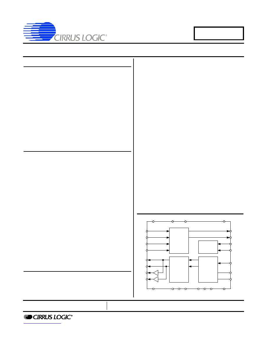
Description
The CS5373A is a high-performance, fourth-order
modulator integrated with a
digital-to-analog convert-
er (DAC). When combined with a CS3301/02 differential
amplifier and the CS5378 digital filter, a small, low-
power, self-testing, high-accuracy, single-channel mea-
surement system results.
The modulator has high dynamic range and low total har-
monic distortion with very low power consumption. It
converts differential analog input signals from the
CS3301/02 amplifier to an oversampled serial bit stream
at 512 kbits per second. This oversampled bit stream is
then decimated by the CS5378 digital filter to a 24-bit
output at the selected output word rate.
The test DAC operates in either AC or DC test modes.
AC test modes measure system dynamic performance
through THD and CMRR tests while DC test modes are
for gain calibration and pulse tests. It has two sets of dif-
ferential analog outputs, OUT and BUF, as dedicated
outputs for testing the electronics channel and for in-
circuit sensor tests. Output attenuation settings are
binary weighted and match the gain settings of the
CS3301/02 differential amplifiers for full-scale testing at
all gain ranges.
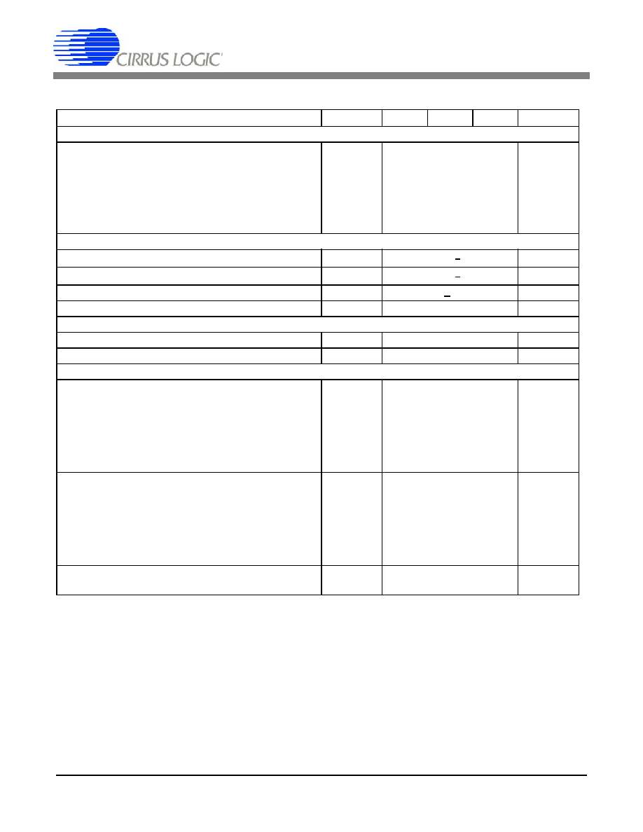
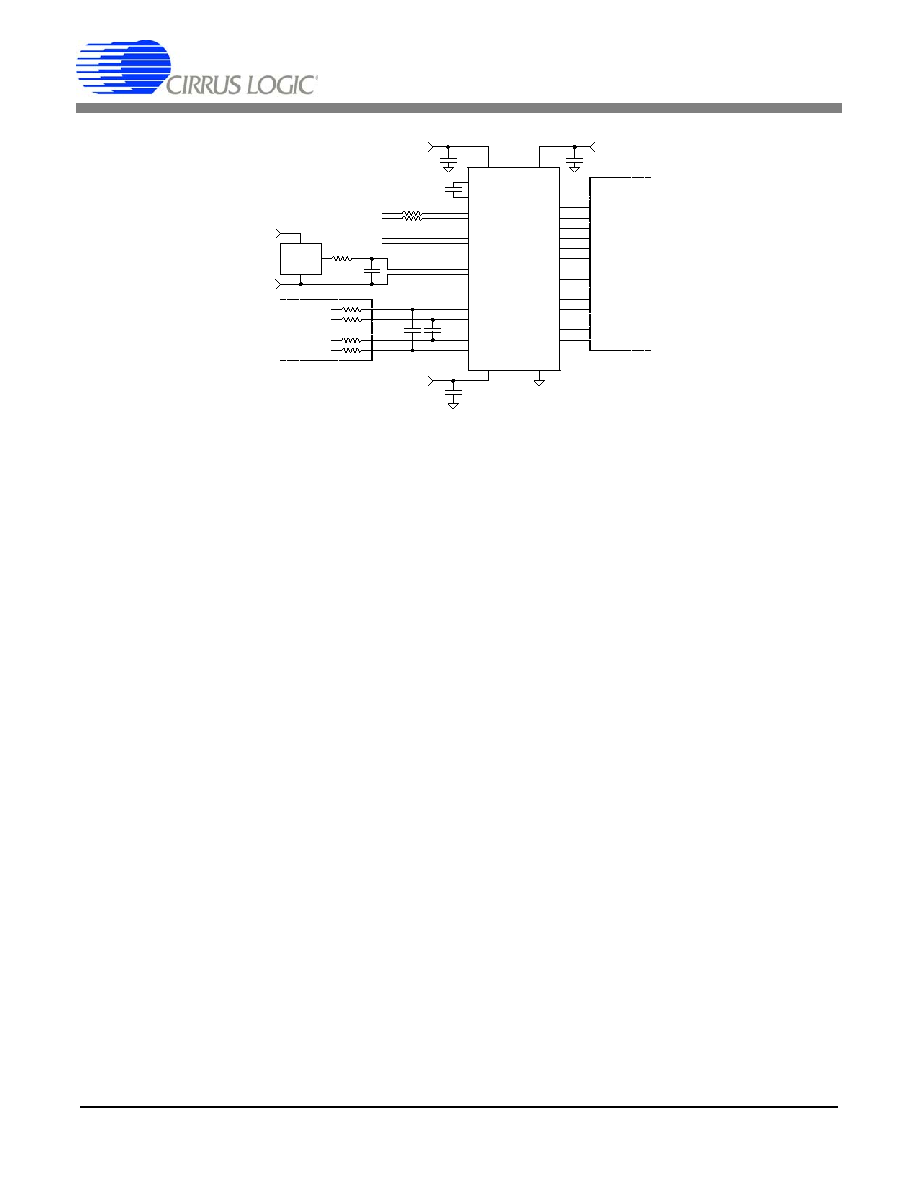
ORDERING INFORMATION
See
page 39
.
24-Bit
Test DAC
Attenuator
1/1 to 1/64
Clock
Generator
VA+
MODE(0, 1, 2)
ATT(0, 1, 2)
VD
VA-
VREF+
VREF-
GND
MCLK
MSYNC
24-Bit
Modulator
OUT+
OUT-
BUF+
BUF-
TDATA
CAP+
CAP-
MDATA
MFLAG
INR+
INF+
INF-
INR-
NOV `05
DS703PP2

CS5373A
2
DS703PP2
TABLE OF CONTENTS
1. CHARACTERISTICS AND SPECIFICATIONS ........................................................................ 4
SPECIFIED OPERATING CONDITIONS ................................................................................. 4
TEMPERATURE CONDITIONS ............................................................................................... 5
ABSOLUTE MAXIMUM RATINGS ........................................................................................... 5
ANALOG INPUT CHARACTERISTICS ................................................................................... 6
ANALOG OUTPUT CHARACTERISTICS ............................................................................... 7
MODULATOR CHARACTERISTICS ........................................................................................ 8
PERFORMANCE PLOTS ......................................................................................................... 9
DAC AC DIFFERENTIAL MODES 1, 2, 3............................................................................... 10
DAC AC DIFFERENTIAL MODES 1, 2, 3 (CONT.) ............................................................... 11
DIGITAL CHARACTERISTICS .............................................................................................. 15
DIGITAL CHARACTERISTICS (CONT.) ............................................................................... 16
DIGITAL CHARACTERISTICS (CONT.) ............................................................................ 17
POWER SUPPLY CHARACTERISTICS ................................................................................ 18
2. GENERAL DESCRIPTION ..................................................................................................... 19
2.1 Delta-Sigma Modulator .................................................................................................... 19
2.2 Digital-to-Analog Converter .............................................................................................. 19
3. SYSTEM DIAGRAM ............................................................................................................ 20
4. POWER MODES ..................................................................................................................... 21
4.1 Power Down ..................................................................................................................... 21
4.2 Sleep Mode ...................................................................................................................... 21
4.3 Modulator Mode ............................................................................................................... 21
4.4 AC Test Modes ................................................................................................................ 21
4.5 DC Test Modes ................................................................................................................ 21
5. OPERATIONAL MODES ........................................................................................................ 22
5.1 Modulator Mode ............................................................................................................... 22
5.1.1 Modulator One's Density ..................................................................................... 22
5.1.2 Modulator Decimated Output .............................................................................. 22
5.1.3 Modulator Synchronization .................................................................................. 22
5.1.4 Modulator Idle Tones .......................................................................................... 23
5.1.5 Modulator Stability ............................................................................................... 23
5.2 AC Test Modes ................................................................................................................ 23
5.2.1 AC Differential ..................................................................................................... 23
5.2.2 AC Common Mode .............................................................................................. 24
5.2.3 DAC Stability ....................................................................................................... 24
5.3 DC Test Modes ................................................................................................................ 24
5.3.1 DC Common Mode ............................................................................................. 24
5.3.2 DC Differential ..................................................................................................... 25
5.4 Sleep Mode ...................................................................................................................... 25
6. DIGITAL SIGNALS ................................................................................................................. 26
6.1 MCLK Connection ............................................................................................................ 26
6.2 MSYNC Connection ......................................................................................................... 26
6.3 MDATA Connection ......................................................................................................... 27
6.4 MFLAG Connection ......................................................................................................... 27
6.5 TDATA Connection .......................................................................................................... 27
6.6 GPIO Connections ........................................................................................................... 27
7. ANALOG SIGNALS ................................................................................................................ 28
7.1 INR±, INF± Modulator Inputs ........................................................................................... 28
7.1.1 Modulator Input Impedance ................................................................................ 28
7.1.2 Modulator Anti-alias Filter ................................................................................... 28
7.2 DAC Output Attenuation .................................................................................................. 29
7.3 DAC OUT± Precision Output ........................................................................................... 29
7.4 DAC BUF± Buffered Output ............................................................................................. 30

CS5373A
DS703PP2
3
7.5 DAC CAP± Connection ................................................................................................... 30
7.6 Analog Differential Signals .............................................................................................. 30
8. VOLTAGE REFERENCE ........................................................................................................ 31
8.1 VREF Power Supply ........................................................................................................ 31
8.2 VREF RC Filter ................................................................................................................ 31
8.3 VREF PCB Routing ......................................................................................................... 31
8.4 VREF Input Impedance ................................................................................................... 31
8.5 VREF Accuracy ............................................................................................................... 32
8.6 VREF Independence ....................................................................................................... 32
9. POWER SUPPLIES ................................................................................................................ 33
9.1 Power Supply Bypassing ................................................................................................. 33
9.2 PCB Layers and Routing ................................................................................................. 33
9.3 Power Supply Rejection .................................................................................................. 33
9.4 SCR Latch-up .................................................................................................................. 34
9.5 DC-DC Converters .......................................................................................................... 34
10. TERMINOLOGY ................................................................................................................... 35
11. PIN DESCRIPTION ............................................................................................................... 36
12. PACKAGE DIMENSIONS .................................................................................................... 38
13. ORDERING INFORMATION ............................................................................................... 39
14. ENVIRONMENTAL, MANUFACTURING, & HANDLING INFORMATION .......................... 39
15. REVISION HISTORY ........................................................................................................... 39
LIST OF FIGURES
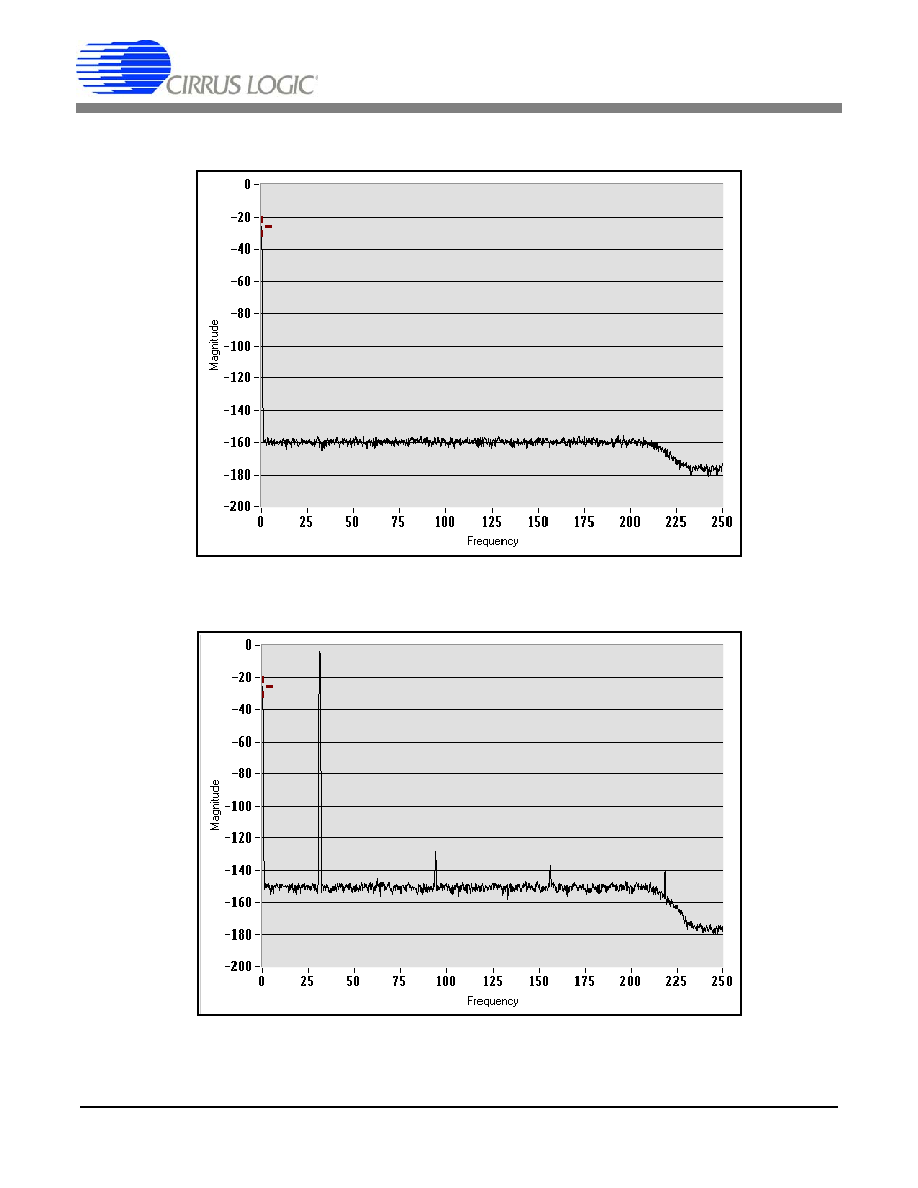
Figure 1. Modulator Noise Performance ......................................................................................... 9
Figure 2. Modulator + Test DAC Dynamic Performance................................................................. 9
Figure 3. Digital Input Rise and Fall Times ................................................................................... 15
Figure 4. System Timing Diagram................................................................................................. 17
Figure 5. MCLK / MSYNC Timing Detail ....................................................................................... 17
Figure 6. CS5373A Block Diagram ............................................................................................... 19
Figure 8. Connection Diagram ...................................................................................................... 20
Figure 7. System Diagram ............................................................................................................ 20
Figure 9. Power Mode Diagram .................................................................................................... 21
Figure 10. AC Differential Modes .................................................................................................. 23
Figure 11. AC Common Mode ...................................................................................................... 24
Figure 12. DC Test Modes ............................................................................................................ 25
Figure 13. Digital Signals .............................................................................................................. 26
Figure 14. Analog Signals ............................................................................................................. 28
Figure 15. DAC Output Attenuation Settings ................................................................................ 29
Figure 16. Voltage Reference Circuit ............................................................................................ 31
Figure 17. Power Supply Diagram ................................................................................................ 33
LIST OF TABLES
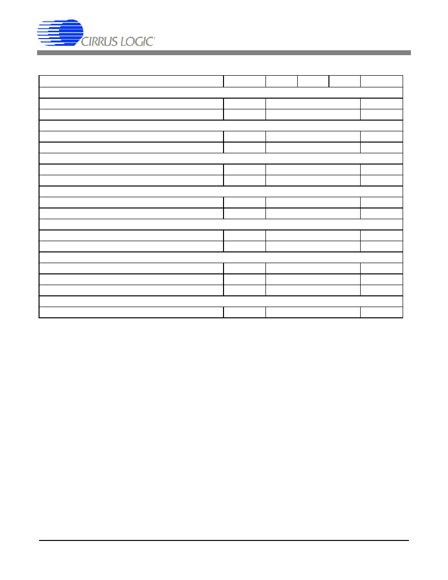
Table 1. Selections for Operational Mode and DAC Attenuation .................................................... 4
Table 2. Operational Modes.......................................................................................................... 22
Table 3. Output Coding for the CS5373A Modulator and CS5378 Digital Filter Combination ...... 22
CS5373A
4
DS703PP2
1.
CHARACTERISTICS AND SPECIFICATIONS
∑
Min / Max characteristics and specifications are guaranteed over the
Specified Operating Conditions
.
∑
Typical performance characteristics and specifications are measured at nominal supply voltages and T
A
= 25
∞C.
∑
GND = 0 V. Single-ended voltages with respect to GND, differential voltages with respect to opposite half.
∑
Device is connected as shown in
Figure 8 on page 20
unless otherwise noted.
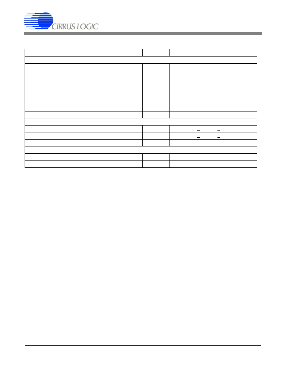
SPECIFIED OPERATING CONDITIONS
Notes: 1. VA- must always be the most-negative input voltage to avoid potential SCR latch-up conditions.
2. By design, a 2.500 V voltage reference input results in the best signal-to-noise performance.
3. Full-scale accuracy is directly proportional to the voltage reference absolute accuracy.
4. VREF inputs must satisfy: VA- < VREF- < VREF+ < VA+.
Parameter
Symbol Min Nom
Max
Unit
Bipolar Power Supplies
Positive Analog
±
2%
VA+
2.45
2.50
2.55
V
Negative Analog
(
Note 1
)
±
2%
VA-
-2.45
-2.50
-2.55
V
Positive Digital
±
3%
VD
3.20
3.30
3.40
V
Voltage Reference
{VREF+} - {VREF-}
(
Note 2, 3
)
VREF
-
2.500
-
V
VREF-
(
Note 4
)
VREF-
-
VA -
-
V
Thermal
Ambient Operating Temperature
Industrial (-IS, -ISZ)
T
A
-40
25
85
∞C
Modes of Operation
Selection
MODE
[2:0]
Mode Description
0
0 0 0
Modulator: enabled.
DAC: sleep.
1
0 0 1
Modulator: enabled.
DAC: AC OUT and BUF outputs.
2
0 1 0
Modulator: enabled.
DAC: AC OUT only, BUF high-z.
3
0 1 1
Modulator: enabled.
DAC: AC BUF only, OUT high-z.
4
1 0 0
Modulator: enabled.
DAC: DC common mode output.
5
1 0 1
Modulator: enabled.
DAC: DC differential output.
6
1 1 0
Modulator: enabled.
DAC: AC common mode output.
7
1 1 1
Modulator: sleep.
DAC: sleep.
DAC Attenuation
Selection
ATT[2:0]
Attenuation
dB
0
0 0 0
1/1
0 dB
1
0 0 1
1/2
-6.02 dB
2
0 1 0
1/4
-12.04 dB
3
0 1 1
1/8
-18.06 dB
4
1 0 0
1/16
-24.08 dB
5
1 0 1
1/32
-30.10 dB
6
1 1 0
1/64
-36.12 dB
7
1 1 1
reserved
reserved
Table 1. Selections for Operational Mode and DAC Attenuation

CS5373A
DS703PP2
5
TEMPERATURE CONDITIONS
ABSOLUTE MAXIMUM RATINGS
WARNING: Operation at or beyond these limits may result in permanent damage to the device.
Normal operation is not guaranteed at these extremes.
Notes: 5. Transient currents up to
±
100 mA will not cause SCR latch-up.
6. Includes continuous over-voltage conditions at the modulator analog input pins.
Parameter
Symbol Min Typ
Max
Unit
Ambient Operating Temperature
T
A
-40
-
85
∫C
Storage Temperature Range
T
STR
-65
-
150
∫C
Allowable Junction Temperature
T
JCT
-
-
125
∫C
Junction to Ambient Thermal Impedance (4-layer PCB)
JA
-
65
-
∫C / W
Parameter
Symbol
Min
Max
Parameter
DC Power Supplies
Positive Analog
Negative Analog
Digital
VA+
VA-
VD
-0.5
-6.8
-0.5
6.8
0.5
6.8
V
V
V
Analog Supply Differential
(VA+) - (VA-)
VA
DIFF
-
6.8
V
Digital Supply Differential
(VD) - (VA-)
VD
DIFF
-
7.6
V
Input Current, Power Supplies
(
Note 5
)
I
PWR
-
±
50
mA
Input Current, Any Pin Except Supplies
(
Note 5, 6
)
I
IN
-
±
10
mA
Output Current
(
Note 5
)
I
OUT
-
±
25
mA
Power Dissipation
PDN
-
500
mW
Analog Input Voltages
V
INA
(VA-) - 0.5
(VA+) + 0.5
V
Digital Input Voltages
V
IND
-0.5
(VD) + 0.5
V
CS5373A
6
DS703PP2
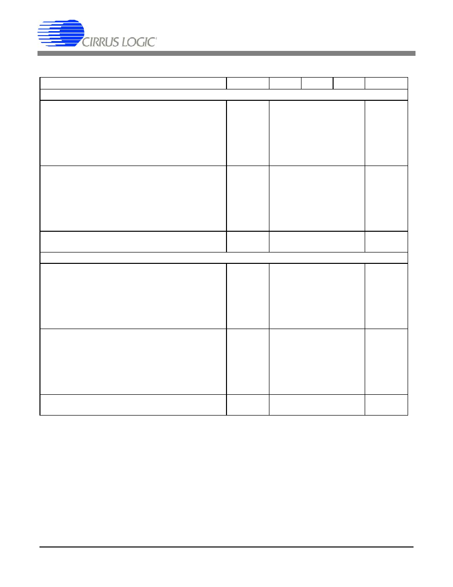
ANALOG INPUT CHARACTERISTICS
Notes: 7. Maximum integrated noise over the measurement bandwidth for the voltage reference device attached
to the VREF
±
inputs.
8. The modulator analog inputs are normally driven by a CS3301/02 amplifier, which has internal anti-alias
series resistors.
9. Differential anti-alias capacitors are discrete external components and must be of good quality (C0G,
NPO, poly). Poor quality capacitors will degrade total harmonic distortion (THD) performance.
Parameter
Symbol Min Typ
Max
Unit
VREF Input
{VREF+} - {VREF-}
(
Note 2, 3
)
VREF
-
2.500
-
V
VREF-
(
Note 4
)
VREF-
-
VA -
-
V
VREF Input Current, Modulator Only
VREF
IMOD
-
120
-
µA
VREF Input Current, Modulator + DAC AC Mode
VREF
IMAC
-
200
-
µA
VREF Input Current, Modulator + DAC DC Mode
VREF
IMDC
-
160
-
µA
VREF Input Noise
(
Note 7
)
VREF
IN
-
-
1
µV
rms
Modulator INR±
,
INF± Inputs
External Anti-alias Filter
Series Resistance
(
Note 8, 9
)
Differential Capacitance
R
AA
C
AA
-
-
680
20
-
-
nF
Differential Input Impedance
INR
±
INF
±
ZDIF
INR
ZDIF
INF
-
-
20
1
-
-
k
M
Single-ended Input Impedance
INR
±
INF
±
ZSE
INR
ZSE
INF
-
-
40
2
-
-
k
M
DAC CAP± Input
External Anti-alias Filter
Differential Capacitance
(
Note 9
)
C
AA
-
10
-
nF

CS5373A
DS703PP2
7
ANALOG OUTPUT CHARACTERISTICS
Notes: 10. Guaranteed by design and/or characterization.
11. Load on the precision OUT± outputs is normally from a CS3301/02 amplifier, which has 2 G
/1 T
typical input impedance and 18 pF typical input capacitance.
12. Single-ended output impedance at 1/64 is different for BUF+ and BUF- due to the output attenuator
architecture.
Parameter
Symbol Min Typ
Max
Unit
DAC Analog OUT±
Output
Analog External Load at OUT
±
Load Resistance
(
Note 10, 11
)
Load Capacitance
R
LOUT
C
LOUT
50
-
-
-
-
50
M
pF
Differential Output Impedance
1/1
1/2
1/4
1/8
1/16
1/32
1/64
ZDIF
OUT
-
-
-
-
-
-
-
1.4
10.1
7.9
5.1
3.3
2.3
1.7
-
-
-
-
-
-
-
k
k
k
k
k
k
k
Single-ended Output Impedance
1/1
1/2
1/4
1/8
1/16
1/32
1/64
ZSE
OUT
-
-
-
-
-
-
-
0.8
7.4
9.0
9.4
9.5
9.5
9.2
-
-
-
-
-
-
-
k
k
k
k
k
k
k
High-Z Impedance
HZ
OUT
-
3
-
M
Crosstalk to BUF
±
High-Z Output
XT
OUT
-
-120
-
dB
DAC Analog BUF± Output
Analog External Load at BUF
±
Load Resistance
(
Note 10
)
Load Capacitance
R
LBUF
C
LBUF
1
-
-
-
-
2
k
nF
Differential Output Impedance
1/1 - 1/64
ZDIF
BUF
-
6
-
Single-ended Output Impedance
1/1 - 1/32
(
Note 12
) (BUF-) 1/64
(
Note 12
) (BUF+) 1/64
ZSE
BUF
-
-
-
4
4
100
-
-
-
High-Z Impedance
HZ
BUF
-
4.5
-
M
Crosstalk to OUT
±
High-Z Output
XT
BUF
-
-120
-
dB
CS5373A
8
DS703PP2
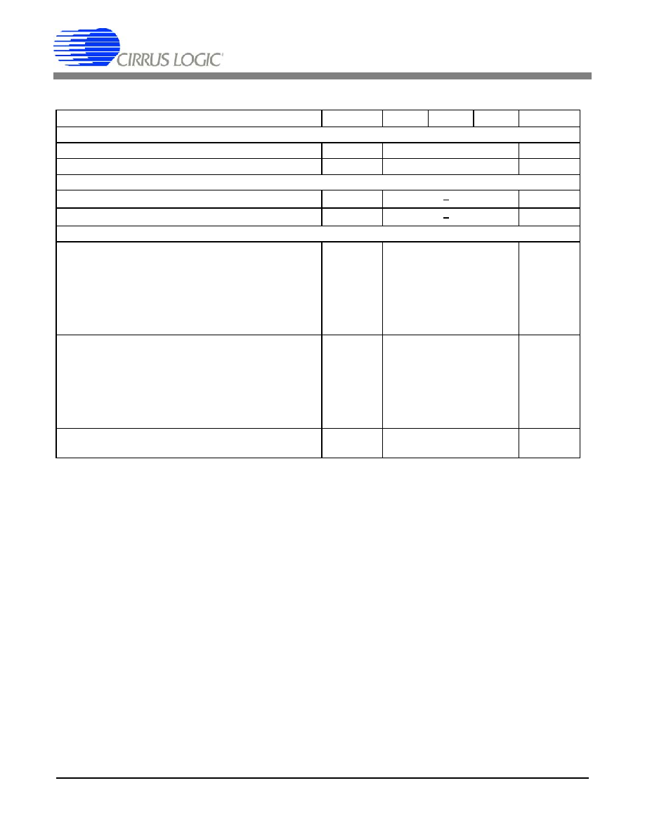
MODULATOR CHARACTERISTICS
Notes: 13. The upper bandwidth limit is determined by the CS5378 digital filter cut-off frequency.
14. No signals operating from external power supplies should be applied to pins of the device prior to its
own supplies being established. Connecting any terminal to voltages greater than VA+ or less than VA-
may cause destructive latch-up.
15. Common mode voltage is defined as the mid-point of the differential signal.
16. Dynamic Range defined as 20 log [ (RMS full scale) / (RMS idle noise) ] where idle noise is measured
from a CS3301/02 amplifier terminated input at 1x gain.
17. Signal Dependent Noise defined as 20 log [ (RMS full scale) / (RMS signal noise) ] where signal noise
is measured by subtracting the signal power at the fundamental and harmonic frequencies.
18. Tested with a 31.25 Hz sine wave at -1 dB amplitude.
19. Specification is for the parameter over the specified temperature range and is for the device only. It does
not include the effects of external components.
20. This specification applies to the effective offset voltage calculated from the output codes of the CS5378
digital filter following offset calibration and correction.
21. Offset calibration is performed in the CS5378 digital filter and includes the full-scale signal range.
Parameter
Symbol Min Typ
Max
Unit
Input Characteristics
Input Signal Frequencies
(
Note 10, 13)
V
BW
DC
-
1720
Hz
Full Scale Differential AC Input
(
Note 10
)
V
AC
-
-
5
V
pp
Full Scale Differential DC Input
(
Note 10
)
V
DC
-2.5
-
2.5
V
dc
Input Voltage Range (Signal + V
cm
)
(
Note 10, 14)
V
RNG
(VA-)+0.7
-
(VA+)-1.25
V
Input Common Mode Voltage
(
Note 15)
V
CM
-
(VA-)+2.5
-
V
Dynamic Performance
Dynamic Range
DC to 1720 Hz
(
Note 16
)
DC to 860 Hz
DC to 430 Hz
DC to 215 Hz
DC to 108 Hz
DC to
54 Hz
DC to
27 Hz
SNR
-
-
121
-
-
-
-
109
121
124
127
130
133
136
-
-
-
-
-
-
-
dB
dB
dB
dB
dB
dB
dB
Signal Dependent Noise
DC to 430 Hz
(
Note 17, 18
)
SDN
100
110
-
dB
Total Harmonic Distortion
(
Note 18
)
THD
-
-118
-112
dB
Linearity
(
Note 18
)
LIN
-
0.000126
0.000251
%
Common Mode Rejection Ratio
CMRR
-
90
-
dB
Gain Accuracy
Channel to Channel Gain Accuracy
(
Note 3
)
CGA
-
±
1
±
2
%
Channel Gain Drift
(
Note 19
)
CGA
TC
-
5
-
ppm/∞C
Offset
Offset Voltage, Differential
OFST
-
100
-
mV
Offset Voltage Drift
(
Note 19
)
OFST
TC
-
0.1
-
µV/∞C
Offset after Calibration
(
Note 20
) OFST
CAL
-
±
1
-
µV
Offset Calibration Range
(
Note 21
) OFST
RNG
-
100
-
%FS
CS5373A
DS703PP2
9
PERFORMANCE PLOTS
Figure 1. Modulator Noise Performance
Figure 2. Modulator + Test DAC Dynamic Performance
CS5373A
10
DS703PP2
DAC AC DIFFERENTIAL MODES 1, 2, 3
Notes: 22. Maximum amplitude for DAC operation above 100 Hz. A reduced amplitude for higher frequencies is
required to guarantee stability of the low-power
DAC architecture.
23. Full-scale accuracy tests the matching of 1/1 attenuation across multiple devices.
24. Relative accuracy tests the tracking of 1/1,1/2,1/4,1/16,1/32,1/64 attenuation relative to 1/8 attenuation
on a single device.
Parameter
Symbol Min Typ
Max
Unit
AC Differential Characteristics
Full-scale Differential AC Output
1/1
1/2
1/4
1/8
1/16
1/32
1/64
VAC
FS
-
-
-
-
-
-
-
5
2.5
1.25
625
312.5
156.25
78.125
-
-
-
-
-
-
-
V
pp
V
pp
V
pp
mV
pp
mV
pp
mV
pp
mV
pp
Full-scale Bandwidth
(
Note 10)
VAC
BW
-
-
100
Hz
Impulse Amplitude
(
Note 10, 22
)
VAC
IMP
-
-
-20
dBfs
AC Differential Accuracy
Full-scale Accuracy
(
Note 3
,
23
)
VAC
ABS
-
+1
+2
%FS
Relative Accuracy
(
Note 24
)
VAC
REL
-
+1
+2
%FS
Full-scale Drift
(
Note 19
)
VAC
TC
-
8
-
µV/∞C
DC Common Mode Characteristics
Common Mode
(
Note 15)
VAC
CM
-
(VA-)+2.35
-
V
Common Mode Drift
(
Note 15
,
19
) VAC
CMTC
-
2
-
µV/∞C
CS5373A
DS703PP2
11
DAC AC DIFFERENTIAL MODES 1, 2, 3 (CONT.)
Notes: 25. Specification measured using CS3301 amplifier at corresponding gain with the modulator measuring a
400 Hz bandwidth. Amplified noise dominates for x16, x32, x64 amplifier gains.
26. Buffered outputs (BUF
±
) include 1/f noise not present on the precision outputs (OUT
±
).
27. Specification measured using CS3301 amplifier at corresponding gain using the modulator measuring
a 400 Hz bandwidth. Amplified noise in the harmonic bins dominates THD measurements for x16, x32,
x64 amplifier gains.
Parameter
Symbol Min Typ
Max
Unit
Signal to Noise
Signal to Noise (OUT
±
Unloaded)
1/1
(
Note 25
) 1/2
1/4
1/8
1/16
1/32
1/64
SNR
OUT
110
-
-
-
-
-
-
114
114
114
113
111
107
102
-
-
-
-
-
-
-
dB
dB
dB
dB
dB
dB
dB
Signal to Noise (BUF
±
Unloaded)
1/1
(
Note 25
,
26
) 1/2
1/4
1/8
1/16
1/32
1/64
SNR
BUF
100
-
-
-
-
-
-
111
107
102
96
90
84
78
-
-
-
-
-
-
-
dB
dB
dB
dB
dB
dB
dB
Signal to Noise (BUF
±
1 k
load)
1/1
(
Note 25
,
26
)
SNR
BUFL
100
110
-
dB
Total Harmonic Distortion
Total Harmonic Distortion (OUT
±
Unloaded)
1/1
(
Note 18
,
27
)
1/2
1/4
1/8
1/16
1/32
1/64
THD
OUT
-
-
-
-
-
-
-
-115
-118
-116
-111
-109
-107
-101
-112
-
-
-
-
-
-
dB
dB
dB
dB
dB
dB
dB
Total Harmonic Distortion (BUF
±
Unloaded)
1/1
(
Note 18
,
26
,
27
)
1/2
1/4
1/8
1/16
1/32
1/64
THD
BUF
-
-
-
-
-
-
-
-111
-107
-102
-97
-92
-86
-80
-95
-
-
-
-
-
-
dB
dB
dB
dB
dB
dB
dB
Total Harmonic Distortion (BUF
±
1 k
load)
1/1
(
Note 18
,
26, 27
)
THD
BUFL
-
-95
-85
dB
CS5373A
12
DS703PP2
DAC DC COMMON MODE 4
Parameter
Symbol Min Typ
Max
Unit
DC Common Mode Characteristics
Common Mode Output
VDC
CM
-
(VA-)+2.35
-
V
Common Mode Drift
(
Note 19
) VDC
CMTC
-
2
-
µV/∞C
DC Common Mode Accuracy
Common Mode Match (OUT
±
)
VDC
CMM
-
+10
-
mV
Common Mode Match (BUF
±
)
VDC
CMM
-
+25
-
mV
Noise
Noise (OUT
±
Unloaded)
1/1
(
Note 25
) 1/2
1/4
1/8
1/16
1/32
1/64
N
OUT
-
-
-
-
-
-
-
4.4
5.6
5.6
5.6
5.6
9.9
17.7
-
-
-
-
-
-
-
µV
rms
µV
rms
µV
rms
µV
rms
µV
rms
µV
rms
µV
rms
Noise (BUF
±
Unloaded)
1/1
(
Note 25
,
26
) 1/2
1/4
1/8
1/16
1/32
1/64
N
BUF
-
-
-
-
-
-
-
5.6
8.9
12.5
28.0
55.9
99.4
198.3
-
-
-
-
-
-
-
µV
rms
µV
rms
µV
rms
µV
rms
µV
rms
µV
rms
µV
rms
Noise (BUF
±
1 k
load)
1/1
(
Note 25
,
26
)
N
BUFL
-
5.6
-
µV
rms
CS5373A
DS703PP2
13
DAC DC DIFFERENTIAL MODE 5
Notes: 28. DC differential output is chopper stabilized and includes low-level 32 kHz out-of-band noise which is
rejected by the digital filter.
Parameter
Symbol Min Typ
Max
Unit
DC Differential Mode Characteristics
Full-scale Differential DC Output
1/1
(
Note 28
)
1/2
1/4
1/8
1/16
1/32
1/64
VDC
FS
-
-
-
-
-
-
-
2.5
1.25
625
312.5
156.25
78.125
39.0625
-
-
-
-
-
-
-
V
V
mV
mV
mV
mV
mV
DC Differential Accuracy
Full-scale Accuracy (OUT
±
)
(
Note 3, 23
)
VDC
OUT
-
VREF +10
-
mV
Full-scale Accuracy (BUF
±
)
(
Note 3, 23
)
VDC
BUF
-
VREF +25
-
mV
Relative Accuracy
(
Note 24
)
VDC
REL
-
+1
-
%FS
Full-scale Drift
(
Note 19
)
VDC
TC
-
8
-
µV/∞C
DC Common Mode Characteristics
Common Mode
(
Note 15
)
VDC
CM
-
(VA-)+2.35
-
V
Common Mode Drift
(
Note 15, 19
) VDC
CMTC
-
2
-
µV/∞C
Noise
Noise (OUT
±
Unloaded)
1/1
(
Note 25
,
28
) 1/2
1/4
1/8
1/16
1/32
1/64
N
OUT
-
-
-
-
-
-
-
6.3
6.3
7.0
7.0
7.0
8.9
12.5
-
-
-
-
-
-
-
µV
rms
µV
rms
µV
rms
µV
rms
µV
rms
µV
rms
µV
rms
Noise (BUF
±
Unloaded)
1/1
(
Note 25
,
26, 28
) 1/2
1/4
1/8
1/16
1/32
1/64
N
BUF
-
-
-
-
-
-
-
9.9
11.2
15.8
28.0
55.9
99.4
198.3
-
-
-
-
-
-
-
µV
rms
µV
rms
µV
rms
µV
rms
µV
rms
µV
rms
µV
rms
Noise (BUF
±
1 k
load)
1/1
(
Note 25
,
26, 28
)
N
BUFL
-
9.9
-
µV
rms
CS5373A
14
DS703PP2
DAC AC COMMON MODE 6
Notes: 29. No AC common mode signal is output at 1/64 attenuation due to the attenuator architecture.
30. Common mode mean is defined as the midpoint between AC common mode peaks.
Parameter
Symbol Min Typ
Max
Unit
AC Common Mode Characteristics
Full-scale Common Mode AC Output
1/1
(
Note 29)
1/2
1/4
1/8
1/16
1/32
VCM
FS
-
-
-
-
-
-
2.5
1.25
625
312.5
156.25
78.125
-
-
-
-
-
-
V
pp
V
pp
mV
pp
mV
pp
mV
pp
mV
pp
Full-scale Bandwidth
(
Note 10)
VCM
BW
-
-
100
Hz
Impulse Amplitude
(
Note 10, 22
)
VCM
IMP
-
-
-20
dBfs
AC Common Mode Accuracy
Common Mode Match (OUT
±
Unloaded)
1/1 - 1/32
(
Note 18
,
27
,
29
)
VCM
CMM
-
-110
-
dB
Common Mode Match (BUF
±
Unloaded)
1/1 - 1/32
(
Note 18
,
26
,
27, 29
)
VCM
CMM
-
-90
-
dB
Common Mode Match (BUF
±
1 k
load)
1/1
(
Note 18
,
26, 29
)
VCM
CMM
-
-90
-
dB
Full-scale Accuracy
(
Note 3
,
23
)
VCM
ABS
-
+1
-
%FS
Relative Accuracy
(
Note 24
)
VCM
REL
-
+1
-
%FS
Full-scale Drift
(
Note 19
)
VCM
TC
-
8
-
µV/∞C
DC Common Mode Characteristics
Common Mode Mean
(
Note 30)
VCM
CM
-
(VA-)+2.35
-
V
Common Mode Mean Drift
(
Note 19, 30
) VCM
CMTC
-
2
-
µV/∞C
CS5373A
DS703PP2
15
DIGITAL CHARACTERISTICS
Notes: 31. Device is intended to be driven with CMOS logic levels.
Parameter
Symbol Min Typ
Max
Unit
Digital Inputs
High-level Input Voltage
(
Note 10, 31
)
V
IH
0.6*VD
-
VD
V
Low-level Input Voltage
(
Note 10, 31
)
V
IL
0.0
-
0.8
V
Input Leakage Current
I
IN
-
±
1
±
10
µA
Digital Input Capacitance
C
IN
-
9
-
pF
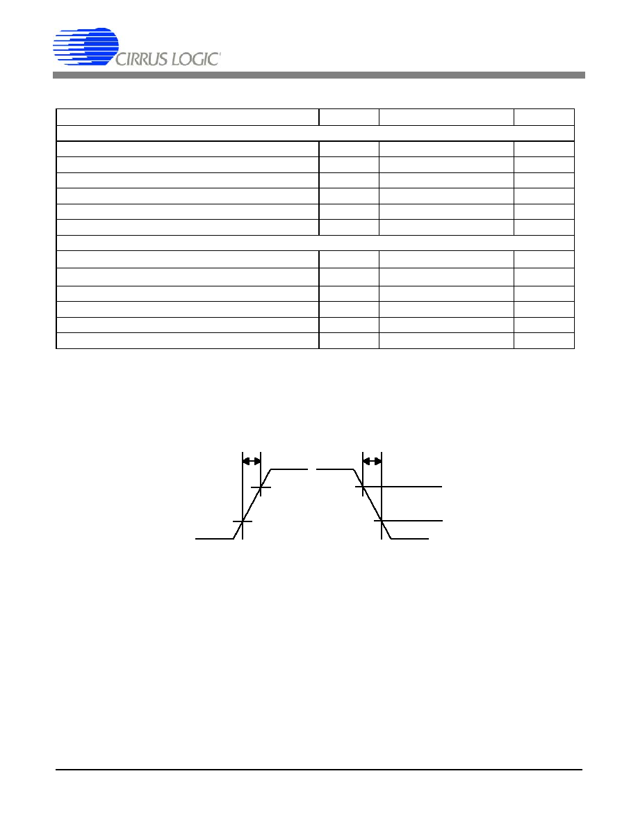
Input Rise Times Except MCLK
(Note 10)
t
RISE
-
-
100
ns
Input Fall Times Except MCLK
(Note 10)
t
FALL
-
-
100
ns
Digital Outputs
High-level Output Voltage, I
out
= -40
µA
(
Note 10
)
V
OH
VD-0.3
-
-
V
Low-level Output Voltage, I
out
= 40
µA
(
Note 10
)
V
OL
-
-
0.3
V
High-Z Leakage Current
I
OZ
-
-
±
10
µA
Digital Output Capacitance
C
OUT
-
9
-
pF
Output Rise Times
(Note 10)
t
RISE
-
-
100
ns
Output Fall Times
(Note 10)
t
FALL
-
-
100
ns
0.9 * VD
0.1 * VD
t fall
t rise
Figure 3. Digital Input Rise and Fall Times
CS5373A
16
DS703PP2
DIGITAL CHARACTERISTICS (CONT.)
Notes: 32. MCLK is generated by the CS5378 digital filter. If MCLK is disabled, the device automatically enters a
power-down state.
33. MSYNC is generated by the CS5378 digital filter and is latched on MCLK rising edge, synchronization
instant (t
0
) on next MCLK rising edge.
34. TDATA can be delayed from 0 to 63 full bit periods by the test bit stream generator in the CS5378 digital
filter. The timing diagrams show no TBSDATA delay.
35. Decimated, filtered, and offset corrected 24-bit output word from the CS5378 digital filter.
36. TDATA is generated by the test bit stream generator in the CS5378 digital filter.
37. TBSGAIN register value in the CS5378 digital filter.
Parameter
Symbol Min Typ
Max
Unit
Master Clock Input
MCLK Frequency
(
Note 32
)
f
CLK
-
2.048
-
MHz
MCLK Period
(
Note 32
)
t
mclk
-
488
-
ns
MCLK Duty Cycle
(
Note 10
)
MCLK
DC
40
-
60
%
MCLK Rise Time
(
Note 10
)
t
RISE
-
-
50
ns
MCLK Fall Time
(
Note 10
)
t
FALL
-
-
50
ns
MCLK Jitter (In-band or aliased in-band)
(
Note 10
)
MCLK
IBJ
-
-
300
ps
MCLK Jitter (Out-of-band)
(
Note 10
) MCLK
OBJ
-
-
1
ns
Master Sync Input
MSYNC Setup Time to MCLK Rising
(
Note 10, 33
)
t
mss
20
122
-
ns
MSYNC Period
(
Note 10, 33
)
t
msync
40
976
-
ns
MSYNC Hold Time after MCLK Falling
(
Note 10, 33
)
t
msh
20
122
-
ns
MSYNC Instant to TDATA Start
(
Note 34
)
t
tdata
-
1220
-
ns
MDATA Output
MDATA Output Bit Rate
f
mdata
-
512
-
kbits/s
MDATA Output One's Density Range
(
Note 10
) MDAT
OD
14
-
86
%
Full-scale Output Code
(
Note 35
)
MDAT
FS
0xA2EAAE
-
0x5D1C41
TDATA Input
TDATA Input Bit Rate
(
Note 36
)
f
tdata
-
256
-
kbits/s
TDATA Input One's Density Range
(
Note 10
)
TBS
OD
25
-
75
%
TBSGAIN Full-scale Code
(
Note 37
)
TBS
FS
-
0x04B8F2
-
TBSGAIN -20 dB Code
(
Note 37
) TBS
-20dB
-
0x0078E5
-
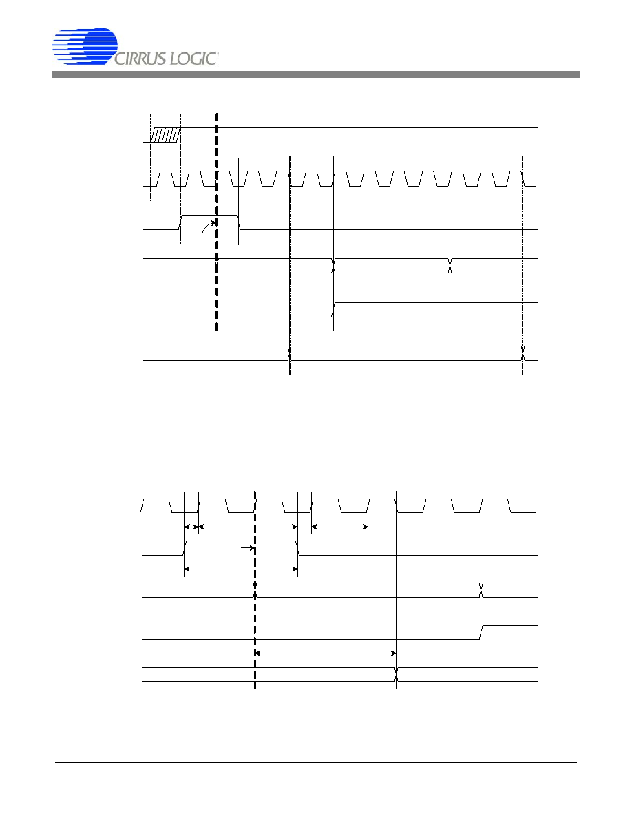
CS5373A
DS703PP2
17
DIGITAL CHARACTERISTICS (CONT.)
MCLK
MSYNC
t
MDATA
TDATA
0
(2.048 MHz)
(512 kHz)
(256 kHz)
SYNC
MFLAG
Figure 4. System Timing Diagram
MCLK
MSYNC
t
TDATA
0
(2.048 MHz)
(256 kHz)
t
mss
t
mclk
t
msync
t
msh
MDATA
(2.048 MHz)
MFLAG
t
tdata
Figure 5. MCLK / MSYNC Timing Detail
CS5373A
18
DS703PP2
POWER SUPPLY CHARACTERISTICS
Notes: 38. All outputs unloaded. Digital inputs forced to VD or GND respectively.
39. Power supply rejection is characterized by applying a 100 mVp-p 50-Hz sine wave to each supply.
Parameter
Symbol Min Typ
Max
Unit
Modulator Power Supply Current
Analog Power Supply Current
(
Note 38
)
I
A
-
5
7
mA
Digital Power Supply Current
(
Note 38
)
I
D
-
200
300
µA
DAC AC Mode Supply Current
Analog Power Supply Current
(
Note 38
)
I
A
-
7.8
10
mA
Digital Power Supply Current
(
Note 38
)
I
D
-
200
-
µA
DAC DC Mode Supply Current
Analog Power Supply Current
(
Note 38
)
I
A
-
4.8
-
mA
Digital Power Supply Current
(
Note 38
)
I
D
-
200
-
µA
Modulator Sleep Current
Analog Power Supply Current
(
Note 38
)
I
A
-
200
-
µA
Digital Power Supply Current
(
Note 38
)
I
D
-
20
-
µA
DAC Sleep Current
Analog Power Supply Current
(
Note 38
)
I
A
-
400
-
µA
Digital Power Supply Current
(
Note 38
)
I
D
-
100
-
µA
Power Down Current (MCLK = 0)
Analog Power Supply Current
(
Note 38
)
I
A
-
100
-
µA
Digital Power Supply Current
(
Note 38
)
I
D
-
20
-
µA
Time to Enter Power Down (MCLK disabled) (
Note 10
)
PD
TC
-
40
-
µS
Power Supply Rejection
Power Supply Rejection Ratio
(
Note 39
)
PSRR
-
90
-
dB
CS5373A
DS703PP2
19
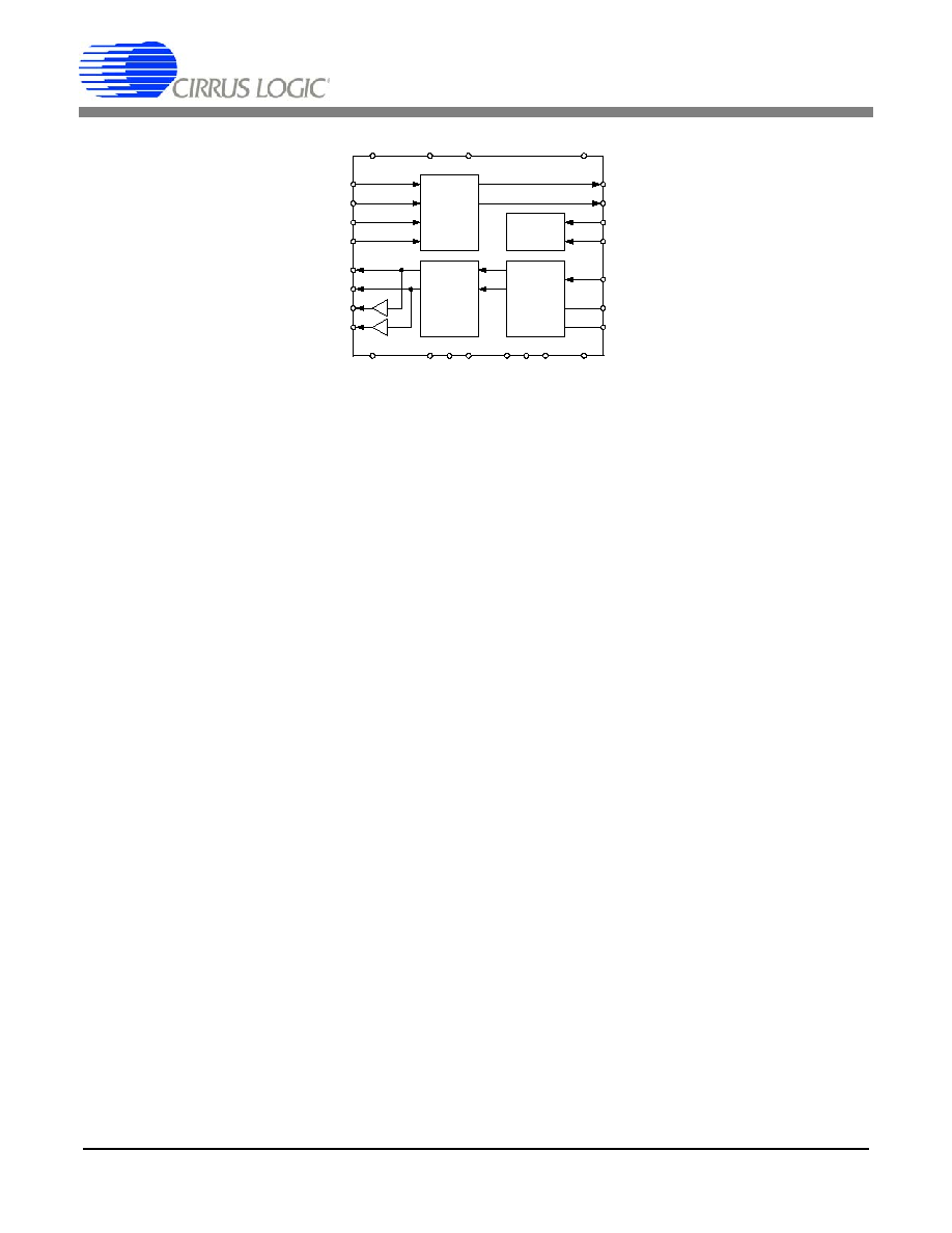
2. GENERAL DESCRIPTION
The CS5373A is a high-performance, fourth-
order
modulator integrated with a digital-to-
analog converter (DAC). When combined with
a CS3301/02 differential amplifier and the
CS5378 digital filter, a small low-power self-
testing high-accuracy single-channel mea-
surement system results.
2.1 Delta-Sigma Modulator
The CS5373A modulator has high dynamic
range and low total harmonic distortion with
very low power consumption, and is optimized
for extremely high-resolution measurement of
5 V
pp
or smaller differential signals. It converts
analog input signals between DC and 1720 Hz
to an oversampled serial bit stream at
512 kbits per second.
The CS5378 digital filter generates the clock
and synchronization inputs for the modulator
while receiving the modulator one-bit data and
over-range flag outputs. The digital filter then
decimates the modulator's oversampled out-
put bit stream to a 24-bit output at the selected
output word rate.
2.2 Digital-to-Analog Converter
The CS5373A test DAC is driven by a digital
bit stream from the CS5378 digital filter's
test bit stream (TBS) generator and operates
in either AC or DC test modes. AC test modes
(MODE 1, 2, 3, 6) are used to measure sys-
tem THD and CMRR performance. DC test
modes (MODE 4, 5) are for gain calibration
and pulse tests. The digital filter also provides
clock and syncronization signals as well as
GPIO control signals to set the operational
mode and analog output attenuation.
Two sets of differential analog outputs, OUT
and BUF, simplify system design as dedicated
outputs for testing the electronics channel and
for in-circuit sensor tests. Output attenuator
settings are binary weighted (1, 1/2, 1/4, 1/8,
1/16, 1/32, 1/64) and match the CS3301/02
amplifier input levels for full-scale testing at all
gain ranges.
For maximum performance, the precision out-
puts (OUT±) must drive only high-impedance
loads such as the CS3301/02 amplifier inputs.
The buffered outputs (BUF±) can drive lower-
impedance loads, down to 1 k
, but with re-
duced performance compared to the precision
outputs.
The test DAC is optimized for low-power oper-
ation and has a restricted operational band-
width in the AC modes. For stable operation,
full-scale AC test signals must not contain fre-
quencies above 100 Hz. AC test signals above
100 Hz (TBS impulse mode, for example)
must have a -20 dB reduced amplitude to en-
sure stability of the low-power
architecture.
24-Bit
Test DAC
Attenuator
1/1 to 1/64
Clock
Generator
VA+
MODE(0, 1, 2)
ATT(0, 1, 2)
VD
VA-
VREF+
VREF-
GND
MCLK
MSYNC
24-Bit
Modulator
OUT+
OUT-
BUF+
BUF-
TDATA
CAP+
CAP-
MDATA
MFLAG
INR+
INF+
INF-
INR-
Figure 6. CS5373A Block Diagram

CS5373A
20
DS703PP2
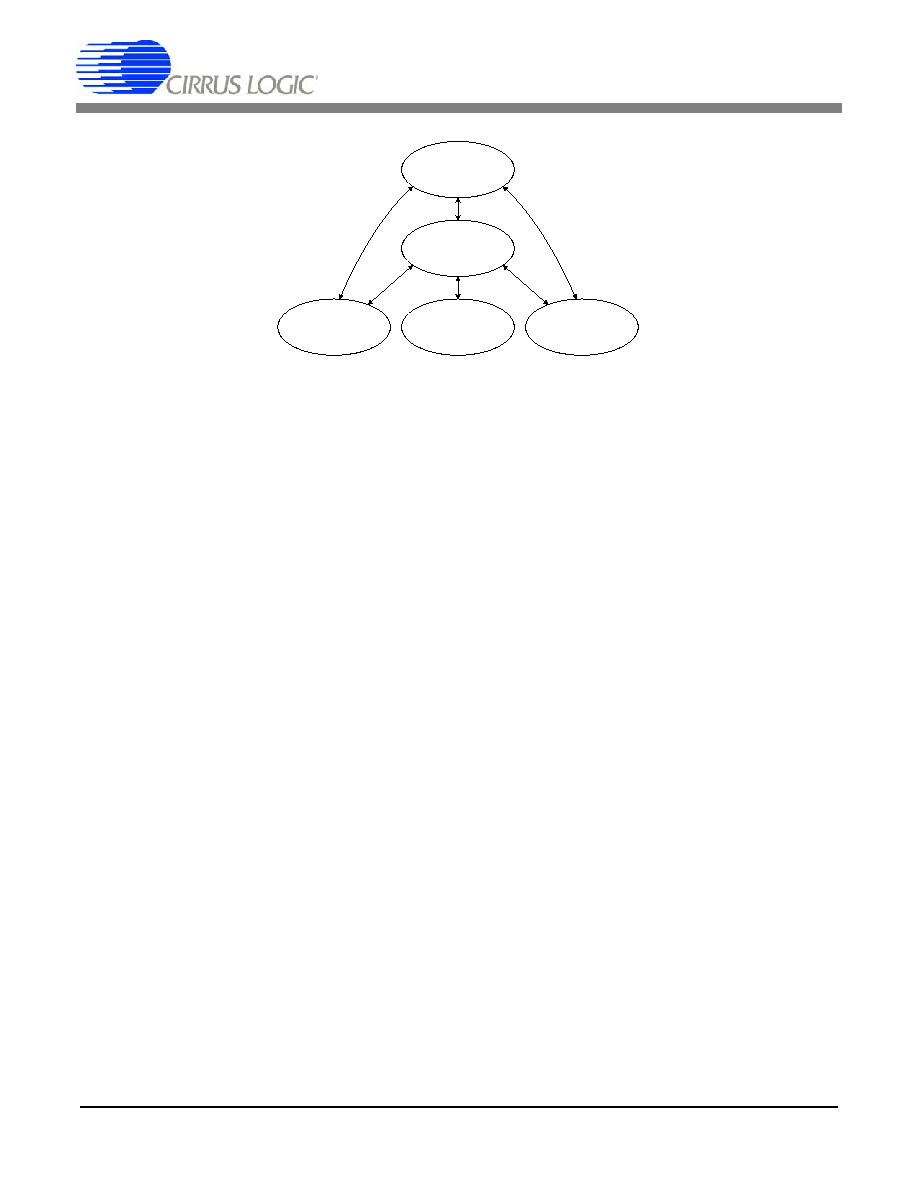
3. SYSTEM DIAGRAM
CS5373A
TDATA
CAP+
CAP-
BUF+
BUF-
OUT+
OUT-
MCLK
MSYNC
GND
MODE1
MODE2
ATT0
ATT1
MODE0
ATT2
VA-
2.5 V
VREF
10
VREF+
VREF-
100µF
0.1µF
VA+
VA+
VD
0.1µF
0.1µF
VD
VA+
10nF
C0G
GPIO
CS5378
SIGNALS
MCLK
MSYNC
TBSDATA
GPIO
GPIO
GPIO
GPIO
GPIO
SENSOR
TEST OUTPUT
ELECTRONICS
TEST OUTPUT
VA-
+
VA-
Route VREF as diff pair
Route OUT as diff pair
Route BUF as diff pair
MDATA
MFLAG
MDATA
MFLAG
INR+
INF+
INF-
INR-
20nF
*
C0G
20nF
*
C0G
INPUT FROM
CS3301/02
AMPLIFIER
*Populate with 2 x 10nF or
1 x 22nF C0G or better.
Figure 8. Connection Diagram
Digital Filter
w/ PLL
AMP
Geophone
or
Hydrophone
Sensor
M
U
X
µController
or
Configuration
EEPROM
Communication
Interface
CS3301
CS3302
CS5378
System
Telemetry
Modulator
and
Test DAC
CS5373A
Figure 7. System Diagram
CS5373A
DS703PP2
21
4. POWER MODES
The CS5373A has five power modes. Modula-
tor mode, AC test modes, and DC test modes
are operational modes, while power down and
sleep mode are non-operational standby
modes.
4.1 Power Down
If MCLK is stopped, an internal loss-of-clock
detection circuit automatically places the
CS5373A into power down. Power down is in-
dependent of the MODE and ATT pin settings,
and is automatically invoked after approxi-
mately 40 µs without an incoming MCLK edge.
In power down the modulator, AC test circuitry
and DC test circuitry are inactive and all out-
puts are high impedance. When used with the
CS5378 digital filter, the CS5373A is in power
down immediately after reset since MCLK is
disabled by default.
4.2 Sleep Mode
With MCLK active, selecting sleep mode
(MODE 7) places the CS5373A into a micro-
power sleep state. In sleep mode the modula-
tor, AC test circuitry and DC test circuitry are
inactive and all outputs are high impedance.
4.3 Modulator Mode
With MCLK active, selecting modulator mode
(MODE 0) enables the CS5373A modulator
and places the AC and DC test circuitry into a
micro-power sleep state with the analog test
outputs high impedance. Following completion
of AC and DC system self-tests, the CS5373A
is typically set into modulator mode for normal
data acquisition.
4.4 AC Test Modes
With MCLK and TDATA active, selecting an
AC test mode (MODE 1, 2, 3, 6) enables the
modulator and causes the DAC to output AC
waveforms on the analog test outputs. AC test
modes use the low-power
DAC circuitry in
the CS5373A to create precision differential or
common mode analog AC output signals from
the encoded digital test bit stream (TBS) input.
4.5 DC Test Modes
With MCLK active, selecting a DC test mode
(MODE 4, 5) enables the modulator and caus-
es the DAC to generate precision DC voltages
on the analog test outputs. DC test modes use
switch-capacitor level-shifting buffer circuitry
in the CS5373A to create differential or com-
mon mode DC analog output voltages from the
voltage reference input.
POWER DOWN
MCLK = OFF
MODE = XXX
SLEEP MODE
MCLK = ON
MODE = 7
AC TEST MODES
MCLK = ON
MODE = 1, 2, 3, 6
DC TEST MODES
MCLK = ON
MODE = 4, 5
MODULATOR MODE
MCLK = ON
MODE = 0
Figure 9. Power Mode Diagram
CS5373A
22
DS703PP2
5. OPERATIONAL MODES
The CS5373A has seven operational modes
and one sleep mode selected by the MODE2,
MODE1, and MODE0 pins.
5.1 Modulator Mode
Modulator mode (MODE 0) enables the
modulator and disables the DAC AC and DC
test circuitry to save power. This mode is used
for normal sensor measurements after self-
tests are completed.
5.1.1
Modulator One's Density
In modulator mode (and whenever the modu-
lator is enabled) the differential analog input
signal is converted to an oversampled
seri-
al bit stream on the MDATA output, with a
one's density proportional to the differential
amplitude of the analog input signal.
One's density of the MDATA output is defined
as the ratio of `1' bits to total bits in the serial
bit stream output, i.e. an 86% one's density
has, on average, a `1' value in 86 of every 100
output data bits. The MDATA output has a
nominal 50% one's density for a mid-scale dif-
ferential input, approximately 86% one's den-
sity for a positive full-scale input, and
approximately 14% one's density for a nega-
tive full-scale input.
5.1.2
Modulator Decimated Output
When the CS5373A modulator operates with
the CS5378 digital filter, the final decimated,
24-bit, full-scale output code range depends if
digital offset correction is enabled. With digital
offset correction enabled, amplifier offset and
the modulator internal offset are removed from
the final conversion result.
5.1.3
Modulator Synchronization
The modulator is designed to operate synchro-
nously with other modulators in a measure-
ment network, so a rising edge on the MSYNC
input resets the internal conversion state ma-
chine to synchronize analog sample timing.
MSYNC is automatically generated by the
CS5378 digital filter after receiving a synchro-
nization signal from the external system, and
is chip-to-chip accurate within ± 1 MCLK peri-
od.
Table 2. Operational Modes
Modes of Operation
Selection
MODE
[2:0]
Mode Description
0
0 0 0
Modulator: enabled.
DAC: sleep.
1
0 0 1
Modulator: enabled.
DAC: AC OUT and BUF outputs.
2
0 1 0
Modulator: enabled.
DAC: AC OUT only, BUF high-z.
3
0 1 1
Modulator: enabled.
DAC: AC BUF only, OUT high-z.
4
1 0 0
Modulator: enabled.
DAC: DC common mode output.
5
1 0 1
Modulator: enabled.
DAC: DC differential output.
6
1 1 0
Modulator: enabled.
DAC: AC common mode output.
7
1 1 1
Modulator: sleep.
DAC: sleep.
Table 3. Output Coding for the CS5373A
Modulator and CS5378 Digital Filter Combination
Modulator
Differential Analog
Input Signal
CS5378 Digital Filter
Output Code
Offset
Corrected
+100 mV
Offset
> + (VREF + 5%)
Error Flag Possible
+ VREF
5D1C41
60D5B4
0 V
000000
03B973
- VREF
A2EAAE
A6A421
> - (VREF + 5%)
Error Flag Possible
CS5373A
DS703PP2
23
5.1.4
Modulator Idle Tones
The CS5373A modulator is
type and so can
produce `idle tones' in the measurement band-
width when the differential input signal is a
steady-state DC signal within ± 50 mV of mid-
scale. Idle tones result from low-frequency
patterns in the output bit stream and appear in
the measurement spectrum as small tones
about -135 dB down from full scale.
Idle tones are eliminated within the CS5373A
modulator by automatically adding +100 mV of
internal differential offset during conversion to
push idle tones out of the measurement band-
width. Care should be taken to ensure external
offset voltages do not negate the internally
added differential offset.
5.1.5
Modulator Stability
The CS5373A's
modulator has a 4
th
order
architecture which is conditionally stable and
may go into an oscillatory condition if the ana-
log inputs are over-ranged more than 5% past
either positive or negative full scale.
If an unstable condition is detected, the modu-
lator collapses to a 1
st
order system and tran-
sitions the MFLAG output low-to-high to signal
an error condition to the CS5378 digital filter.
The analog input signal must be reduced to
within the full-scale range for at least 32 MCLK
cycles for the modulator to recover from an os-
cillatory condition. If the analog input remains
over-ranged for an extended period, the mod-
ulator will cycle between 4
th
order and 1
st
or-
der operation and the MFLAG output will be
seen to pulse.
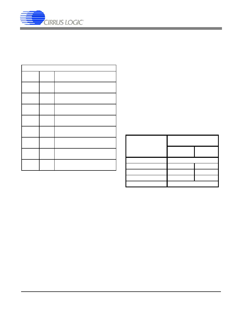
5.2 AC Test Modes
AC test modes (MODE 1, 2, 3, 6) enable the
modulator and use the digital test bit stream
(TBS) input from the CS5378 digital filter to
construct analog AC waveforms. The digital bit
stream input to the TDATA pin encodes the
analog waveform as over-sampled one-bit
data, which is then converted into precision
differential or common mode analog AC sig-
nals by the CS5373A's test DAC.
5.2.1
AC Differential
The first three AC test modes (MODE 1, 2, 3)
enable the modulator and AC test circuitry to
create precision differential analog signals for
THD and impulse testing of the measurement
channel. In mode 1, both sets of differential an-
alog outputs (OUT and BUF) are enabled. In
mode 2 only the OUT analog output is en-
abled, and the BUF output is high impedance.
In mode 3 only the BUF analog output is en-
abled, and the OUT output is high impedance.
OUT+
OUT-
BUF+
BUF-
CS5373A
MODE 1
Maximum
5 Vpp
Differential
Maximum
5 Vpp
Differential
OUT+
OUT-
BUF+
BUF-
CS5373A
MODE 2
Maximum
5 Vpp
Differential
High
Impedance
OUT+
OUT-
BUF+
BUF-
CS5373A
MODE 3
High
Impedance
Maximum
5 Vpp
Differential
Figure 10. AC Differential Modes
CS5373A
24
DS703PP2
Differential AC test signals out of the CS5373A
consist of two halves with equal but opposite
magnitude, varying about a common mode
voltage. A full-scale 5 V
PP
differential AC sig-
nal centered on a -0.15 V common mode volt-
age will have:
SIG+ = -0.15 V + 1.25 V = +1.1 V
SIG- = -0.15 V - 1.25 V = -1.4 V
SIG+ is +2.5 V relative to SIG-
For the opposite case:
SIG+ = -0.15 V - 1.25 V = -1.4 V
SIG- = -0.15 V + 1.25 V = +1.1 V
SIG+ is -2.5 V relative to SIG-
So the total swing for SIG+ relative to SIG- is
(+2.5 V) - (-2.5 V) = 5 V
pp
differential. A similar
calculation can be done for SIG- relative to
SIG+. It's important to note that a 5 V
pp
differ-
ential signal centered on a -0.15 V common
mode voltage never exceeds +1.1 V with re-
spect to ground and never drops below -1.4 V
with respect to ground on either half. By defini-
tion, differential voltages are measured with
respect to the opposite half, not relative to
ground. A voltmeter differentially measuring
between SIG+ and SIG- in the above example
would correctly read 1.767 V
rms
, or 5 V
pp
.
5.2.2
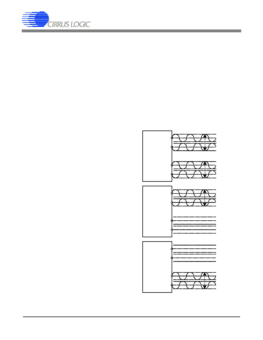
AC Common Mode
The final AC test mode (MODE 6) enables the
modulator and AC test circuitry to create a
matched AC common mode analog signal for
CMRR testing of the measurement channel. In
mode 6, both sets of analog outputs (OUT and
BUF) are enabled. There is no AC common
mode output for an attenuator setting of 1/64.
Gross leakage in the sensor channel can be
detected by applying a full-scale AC common
mode signal. If there is a significant differential
mismatch in the channel due to sensor leak-
age, the AC common mode signal will be con-
verted to a measurable differential signal at
the fundamental frequency.
5.2.3
DAC Stability
For the CS5373A's low-power
DAC archi-
tecture to remain stable, the TDATA input bit
stream should only encode 100 Hz or lower
bandwidth analog signals. For TDATA bit
stream frequencies above 100 Hz (for exam-
ple, TBS impulse mode), the encoded ampli-
tude must be reduced -20 dB below full scale
to guarantee stability.
If the CS5373A's low-power
DAC architec-
ture becomes unstable, persistent elevated
noise will be present on the analog outputs
and AC linearity will be poor. To recover stabil-
ity, place the CS5373A into power down or
sleep mode and restart the CS5378 test bit
stream generator before placing the CS5373A
back into an AC test mode.
5.3 DC Test Modes
DC test modes enable the modulator and DC
test circuitry to create precision level-shifted
and buffered versions of the voltage reference
input as precision DC common mode and DC
differential analog outputs. The absolute accu-
racy of the DC test modes is highly dependent
on the absolute accuracy of the voltage refer-
ence input voltage.
5.3.1
DC Common Mode
The first DC test mode (MODE 4) enables the
modulator and DC test circuitry to create a
matched DC common mode analog output
voltage as a baseline measurement for gain
OUT+
OUT-
BUF+
BUF-
CS5373A
MODE 6
Maximum
2.5 Vpp
Common
Mode
Maximum
2.5 Vpp
Common
Mode
Figure 11. AC Common Mode
CS5373A
DS703PP2
25
calibration and differential pulse tests. In mode
4, both sets of analog outputs (OUT and BUF)
are enabled.
5.3.2
DC Differential
The second DC test mode (MODE 5) enables
the modulator and DC test circuitry to create a
precision differential DC analog output voltage
as the final measurement for gain calibration
and as the step/pulse output for differential
pulse tests. In mode 5, both sets of analog out-
puts (OUT and BUF) are enabled.
In DC differential mode (MODE 5) the level-
shifting buffer circuitry adds low-level 32 kHz
switched-capacitor noise to the DC output.
This noise is out of the measurement band-
width for systems designed with a CS3301/02
amplifier and CS5373A modulator and is re-
jected by the CS5378 digital filter. This 32 kHz
switched-capacitor noise does not affect DC
system tests, though it may be visible on an
oscilloscope at high gain levels.
By measuring both DC test modes
(MODE 4, 5), precision gain-calibration coeffi-
cients can be calculated for the measurement
channel. By first measuring the differential off-
set of the DC common mode output (MODE 4)
and then measuring the DC differential mode
amplitude (MODE 5), a precise offset-correct-
ed, volts-to-codes conversion ratio can be cal-
culated. This known ratio is then used along
with the CS5378 digital filter GAIN register to
normalize the full-scale amplitude to match
other channels in the measurement network.
By switching between DC common mode
(MODE 4) and DC differential mode
(MODE 5), pulse waveforms can be created to
characterize the step response of the mea-
surement channel. If a pulse test requires pre-
cise timing control, an external controller
should directly toggle the MODE pins of the
CS5373A to avoid delays associated with writ-
ing to the CS5378 digital filter GPIO register.
Sensor impedance can be measured using
DC differential mode (MODE 5), provided
matched series resistors are installed between
the BUF analog outputs and the sensor. Ap-
plying the known DC differential voltage to the
resistor-sensor-resistor string permits a ratio-
metric sensor impedance calculation from the
measured voltage drop across the sensor.
Switching between DC differential mode
(MODE 5) and modulator mode (MODE 0)
can, in the case of a moving-coil geophone,
test basic parameters of the electro-mechani-
cal transfer function. The voltage relaxation
characteristic of the sensor when switching the
analog outputs from a differential DC voltage
to high impedance depends primarily on the
geophone resonant frequency and damping
factor.
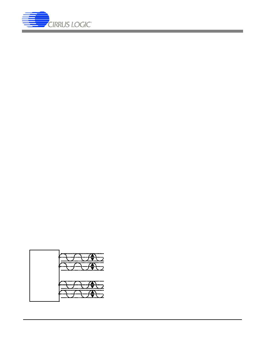
5.4 Sleep Mode
Sleep mode (MODE 7) saves system power
when measurements are not required by turn-
ing off the modulator, AC test circuitry, and DC
test circuitry. In sleep mode the modulator dig-
ital outputs and the BUF and OUT analog out-
puts are high impedance.
OUT+
OUT-
BUF+
BUF-
CS5373A
MODE 4
Approx
-0.15 V
DC
Common
Mode
Approx
-0.15 V
DC
Common
Mode
OUT+
OUT-
BUF+
BUF-
CS5373A
MODE 5
Maximum
2.5 V
DC
Differential
Maximum
2.5 V
DC
Differential
Figure 12. DC Test Modes
CS5373A
26
DS703PP2
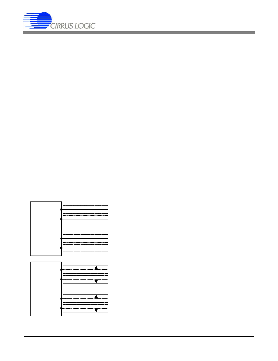
6. DIGITAL SIGNALS
The CS5373A is designed to operate with the
CS5378 digital filter. The digital filter gener-
ates the master clock and synchronization sig-
nals (MCLK and MSYNC) while receiving back
the modulator one-bit
conversion data
(MDATA) and over-range flag (MFLAG). It
also generates digital one-bit
test bit
stream data for the test DAC (TDATA) and
controls GPIO pins to set the operational
mode (MODE) and attenuation (ATT).
6.1 MCLK Connection
The CS5378 digital filter generates the master
clock for CS5373A, typically 2.048 MHz, from
a synchronous CLK input from the external
system. By default, MCLK is disabled at reset
and is enabled by writing the digital filter CON-
FIG register. If MCLK is disabled during oper-
ation, the CS5373A will enter power down
after approximately 40
µ
S.
MCLK must have low in-band jitter to guaran-
tee full analog performance, requiring a crys-
tal- or VCXO-based system clock into the
digital filter. Clock jitter on the digital filter ex-
ternal CLK input directly translates to jitter on
MCLK.
6.2 MSYNC Connection
The CS5378 digital filter also provides a syn-
chronization signal to the CS5373A. The
MSYNC signal is generated following a rising
edge received on the digital filter SYNC input.
By default MSYNC generation is disabled at
reset and is enabled by writing to the digital fil-
ter CONFIG register.
The input SYNC signal to the CS5378 digital
filter sets a common reference time t
0
for mea-
surement events, thereby synchronizing ana-
log sampling across a measurement network.
The timing accuracy of the received SYNC sig-
nal from node to node must be +/- 1 MCLK to
maximize the MSYNC analog sample syn-
chronization accuracy.
The CS5373A MSYNC input is rising-edge
triggered and resets the internal MCLK
counter/divider to guarantee synchronous op-
eration with other system devices. While the
MSYNC signal synchronizes the internal oper-
ation of the CS5373A, by default, it does not
synchronize the phase of the incoming encod-
ed digital test bit stream (TBS) sine wave un-
less enabled in the digital filter TBSCFG
register.
CS5373A
TDATA
CAP+
CAP-
BUF+
BUF-
OUT+
OUT-
MCLK
MSYNC
GND
MODE1
MODE2
ATT0
ATT1
MODE0
ATT2
VA-
2.5 V
VREF
10
VREF+
VREF-
100µF
0.1µF
VA+
VA+
VD
0.1µF
0.1µF
VD
VA+
10nF
C0G
GPIO
CS5378
SIGNALS
MCLK
MSYNC
TBSDATA
GPIO
GPIO
GPIO
GPIO
GPIO
SENSOR
TEST OUTPUT
ELECTRONICS
TEST OUTPUT
VA-
+
VA-
Route VREF as diff pair
Route OUT as diff pair
Route BUF as diff pair
MDATA
MFLAG
MDATA
MFLAG
INR+
INF+
INF-
INR-
20nF
*
C0G
20nF
*
C0G
INPUT FROM
CS3301/02
AMPLIFIER
*Populate with 2 x 10nF or
1 x 22nF C0G or better.
Figure 13. Digital Signals

CS5373A
DS703PP2
27
6.3 MDATA Connection
The CS5373A modulator outputs a
serial
bit stream to the MDATA pin, with a one's den-
sity proportional to the differential amplitude of
the analog input signal. The output bit rate
from the MDATA output is a divide-by-four of
the input master clock, and so is nominally
512 kHz.
The MDATA output has a nominal 50% one's
density for mid-scale input, approximately
86% one's density for a positive full-scale in-
put, and approximately 14% one's density for
a negative full-scale input. One's density of the
MDATA output is defined as the ratio of `1' bits
to total bits in the serial bit stream output, i.e.
an 86% one's density has, on average, a `1'
value in 86 of every 100 output data bits.
6.4 MFLAG Connection
The CS5373A
modulator has a 4
th
order ar-
chitecture which is conditionally stable and
may go into an oscillatory condition if the ana-
log inputs are over-ranged more than 5% past
either positive or negative full-scale.
If an unstable condition is detected, the modu-
lator collapses to a 1
st
order system and tran-
sitions the MFLAG output low-to-high to signal
an error condition to the CS5378 digital filter.
The analog signal must be reduced to within
the full-scale input range for at least 32 MCLK
cycles for the modulator to recover from an os-
cillatory condition. If the analog input remains
over-ranged for an extended period, the mod-
ulator will cycle between 4
th
order and 1
st
or-
der operation and the MFLAG output will be
seen to pulse.
The MFLAG output connects to a dedicated in-
put on the CS5378 digital filter, causing an er-
ror flag to be set in the status portion of the
next conversion output data word.
6.5 TDATA Connection
The TDATA digital input to the test DAC ex-
pects encoded one-bit
data nominally at a
256 kHz rate. The one's density input range is
approximately 25% minimum to 75% maxi-
mum, with differential mid-scale at 50% one's
density.
The CS5378 digital filter test bit stream (TBS)
generator can encode two types of AC signals
as over-sampled, one-bit
data ≠ a pure sine
wave for THD and CMRR testing or a trigger-
able impulse waveform for synchronization
testing and impulse response characteriza-
tion. In the AC test modes, the test DAC con-
verts the over-sampled test bit stream digital
data into precision differential or common
mode analog AC signals.
The CS5378 TBS sine mode encodes an ap-
proximately 5 V
pp
full-scale sine wave signal
with a digital filter TBSGAIN register setting of
0x04B8F2. Because TBS impulse mode en-
codes frequencies above 100 Hz, a maximum
0x0078E5 TBSGAIN impulse mode register
setting is specified to guarantee stability of the
DAC low-power
circuitry. Details on the set-
up and operation of the digital filter test bit-
stream (TBS) generator can be found in the
CS5378 data sheet.
6.6 GPIO Connections
The CS5378 controls 8 general-purpose input
output (GPIO) pins through the digital filter
GPCFG register. These GPIO pins are typical-
ly assigned to operate the CS5373A mode and
attenuator pins, along with the CS3301/02 am-
plifier input mux and gain pins. The gain and
attenuation settings of the CS3301/02 amplifi-
ers and the CS5373A test DAC are identically
decoded to allow full-scale performance test-
ing at all system gain ranges with shared GAIN
and ATT control signals.
If precise timing control of operational modes
is required (for example, switching between
DC modes for pulse generation), an external
controller should directly toggle the MODE
pins of the CS5373A to avoid the delay asso-
ciated with writing to the CS5378 digital filter
GPCFG register.

CS5373A
28
DS703PP2
7. ANALOG SIGNALS
The CS5373A has multiple differential analog
inputs and outputs. The modulator analog in-
puts are separated into rough and fine charge
differential pairs (INR±, INF±) for maximum
sampling accuracy. Both sets of modulator in-
puts require a simple differential anti-alias RC
filter to ensure high-frequency signals do not
alias into the measurement bandwidth.
The test DAC has a precision differential out-
put (OUT±) that provides the best analog per-
formance, but with only minimal drive
capability. A buffered output (BUF±) can drive
an external load, but with reduced analog per-
formance. Finally, the test DAC internal anti-
alias filter requires a dedicated capacitor con-
nection (CAP±) to eliminate undesired high-
frequency signals.
7.1 INR±, INF± Modulator Inputs
The modulator analog inputs are separated
into differential rough and fine signals (INR±,
INF±). The positive half of the differential input
signal is connected to INR+ and INF+, while
the negative half is attached to INF- and INR-.
The INR± pins are switched-capacitor `rough
charge' inputs that pre-charge the internal an-
alog sampling capacitor before it is connected
to the INF± fine input pins.
7.1.1
Modulator Input Impedance
The modulator input has a dynamic switched-
capacitor architecture and so has a rough
charge input impedance that is inversely pro-
portional to the input master clock frequency
and the input capacitor size, [1 / (f * C)].
Internal to the modulator, the rough inputs
(INR±) pre-charge the sampling capacitor
used by the fine inputs (INF±), therefore the in-
put current to the fine inputs is very low and the
effective input impedance is orders of magni-
tude above the impedance of the rough inputs.
7.1.2
Modulator Anti-alias Filter
The modulator inputs are required to be band-
width limited to ensure modulator loop stability
and prevent high-frequency signals from alias-
ing into the measurement band. The use of
simple single-pole differential low-pass RC fil-
ters across the INR± and INF± inputs ensures
high-frequency signals are rejected before
they can alias into the measurement band.
CS5373A
TDATA
CAP+
CAP-
BUF+
BUF-
OUT+
OUT-
MCLK
MSYNC
GND
MODE1
MODE2
ATT0
ATT1
MODE0
ATT2
VA-
2.5 V
VREF
10
VREF+
VREF-
100µF
0.1µF
VA+
VA+
VD
0.1µF
0.1µF
VD
VA+
10nF
C0G
GPIO
CS5378
SIGNALS
MCLK
MSYNC
TBSDATA
GPIO
GPIO
GPIO
GPIO
GPIO
SENSOR
TEST OUTPUT
ELECTRONICS
TEST OUTPUT
VA-
+
VA-
Route VREF as diff pair
Route OUT as diff pair
Route BUF as diff pair
MDATA
MFLAG
MDATA
MFLAG
INR+
INF+
INF-
INR-
20nF
*
C0G
20nF
*
C0G
INPUT FROM
CS3301/02
AMPLIFIER
*Populate with 2 x 10nF or
1 x 22nF C0G or better.
Figure 14. Analog Signals
∑
MCLK = 2.048 MHz
∑
INR± Input Cap = 20 pF
∑
Impedance = [1 / (2.048 MHz * 20 pF)] = 24 k
.
CS5373A
DS703PP2
29
The -3 dB corner of the input anti-alias filter is
nominally set to the internal analog sampling
rate divided by 64, which itself is a division by
4 of the MCLK input rate.
Figure 14 illustrates the CS5373A modulator
analog connections with input anti-alias filter
components. Filter components on the rough
and fine pins should be identical values for op-
timum performance, with the capacitor values
a minimum of 0.02
µF. The rough input can
use either X7R or C0G type capacitors, while
the fine input requires C0G type capacitors for
optimal linearity. Using X7R type capacitors on
the fine analog inputs will degrade total har-
monic distortion significantly.
The CS3301/02 differential amplifiers are de-
signed with separate rough and fine analog
outputs (OUTR±, OUTF±) that match the
rough and fine inputs to the modulator (INR±,
INF±). Internal anti-alias series resistors are
included in the amplifier analog outputs, so
only external differential capacitors are re-
quired to create the anti-alias RC filters.
7.2 DAC Output Attenuation
The CS5373A test DAC has seven analog out-
put attenuation settings from 1/1 to 1/64 se-
lected with the ATT2, ATT1, and ATT0 pins.
When enabled, attenuation is applied to both
the OUT± and BUF± differential analog out-
puts. At 1/64 attenuation in AC Common Mode
(MODE 6) there is no output signal amplitude
due to the attenuator architecture.
The OUT± pins connect directly into the inter-
nal attenuator resistors and so attenuation ac-
curacy is highly sensitive to load impedance
on the OUT± pins. Loading on the BUF± pins
does not affect attenuator accuracy.
The attenuation settings of CS5373A match
the gain ranges of the CS3301/02 differential
amplifiers to enable full-scale testing at all gain
ranges. The CS3301/02 amplifier gain settings
(GAIN) are decoded identical to the CS5373A
attenuator settings (ATT) and so can share
GPIO control signals from the CS5378 digital
filter.
7.3 DAC OUT± Precision Output
The test DAC OUT± pins are precision differ-
ential analog outputs for testing the high-per-
formance electronics measurement channel.
These precision outputs have higher perfor-
mance specifications than the BUF± outputs,
but with a much higher sensitivity to external
loading. Excessive resistive or capacitive load-
ing on the OUT± pins will degrade the analog
performance characteristics of the test DAC in
all operational modes.
The OUT± precision output is optimized for di-
rect connection to the CS3301/02 amplifier dif-
ferential inputs, which have very high input
impedance. These amplifiers include a pin-
controlled input multiplexer to switch between
an internal differential termination for noise
tests and two external differential inputs. One
∑
MCLK Frequency = 2.048 MHz
∑
Sampling Frequency = MCLK / 4 = 512 kHz
∑
-3 dB Filter Corner = Sample Freq / 64 = 8 kHz
∑
RC filter = 8 kHz = 1 / [ 2
* (2 * R
series
) * C
diff
)]
Figure 15. DAC Output Attenuation Settings
Selection ATT[2:0]
Attenuation
dB
0
0 0 0
1/1
0 dB
1
0 0 1
1/2
-6.02 dB
2
0 1 0
1/4
-12.04 dB
3
0 1 1
1/8
-18.06 dB
4
1 0 0
1/16
-24.08 dB
5
1 0 1
1/32
-30.10 dB
6
1 1 0
1/64
-36.12 dB
7
1 1 1
reserved
reserved

CS5373A
30
DS703PP2
external input is typically dedicated to sensor
measurements and the other to testing the
electronics channel.
The OUT± outputs are enabled in all opera-
tional modes except modulator mode
(MODE 0), "AC BUF Only" mode (MODE 3)
and sleep mode (MODE 7). In modulator
mode, AC BUF Only mode and sleep mode
the OUT± pins are high impedance.
7.4 DAC BUF± Buffered Output
The test DAC BUF± pins are buffered differen-
tial analog outputs for testing external sensors
such as geophones or hydrophones. The buff-
ered outputs have reduced performance spec-
ifications compared with the OUT± outputs,
but are less sensitive to external loading.
The BUF± outputs are enabled in all operation-
al modes except modulator mode (MODE 0),
"AC OUT Only" mode (MODE 2) and sleep
mode (MODE 7). In modulator mode,
AC OUT only and sleep mode the BUF± pins
are high impedance to ensure they do not in-
terfere with sensor operation during normal
data acquisition.
For sensor impedance testing, it is required to
place matched series resistors in between the
BUF± outputs and the differential sensor. With
known series resistors and a known DC differ-
ential source voltage, sensor resistance can
be calculated ratiometrically from the mea-
sured voltage drop across the sensor.
7.5 DAC CAP± Connection
The CS5373A test DAC requires a 10 nF C0G
type capacitor to be connected differentially
across the CAP± pins. This capacitor creates
an internal anti-alias filter to eliminate high-fre-
quency signals from the OUT± and BUF± ana-
log outputs and helps to maintain the stability
of the low-power
DAC circuitry.
A COG, NPO or similar high-quality capacitor
is required for CAP
±
since other capacitor
types, such as X7R, do not have the required
linearity. Using a poor-quality capacitor on
CAP± will significantly degrade THD perfor-
mance of the test DAC AC operational modes.
7.6 Analog Differential Signals
Differential AC test signals into and out of the
CS5373A consist of two halves with equal but
opposite magnitude varying about a common
mode voltage. A full-scale 5 V
PP
differential
AC signal centered on a -0.15 V common
mode voltage will have:
SIG+ = -0.15 V + 1.25 V = +1.1 V
SIG- = -0.15 V - 1.25 V = -1.4 V
SIG+ is +2.5 V relative to SIG-
For the opposite case:
SIG+ = -0.15 V - 1.25 V = -1.4 V
SIG- = -0.15 V + 1.25 V = +1.1 V
SIG+ is -2.5 V relative to SIG-
So the total swing for SIG+ relative to SIG- is
(+2.5 V) - (-2.5 V) = 5 V
pp
differential. A similar
calculation can be done for SIG- relative to
SIG+. It's important to note that a 5 V
pp
differ-
ential signal centered on a -0.15 V common
mode voltage never exceeds +1.1 V with re-
spect to ground and never drops below -1.4 V
with respect to ground on either half. By defini-
tion, differential voltages are measured with
respect to the opposite half, not relative to
ground. A voltmeter differentially measuring
between SIG+ and SIG- in the above example
would correctly read 1.767 V
rms
, or 5 V
pp
.
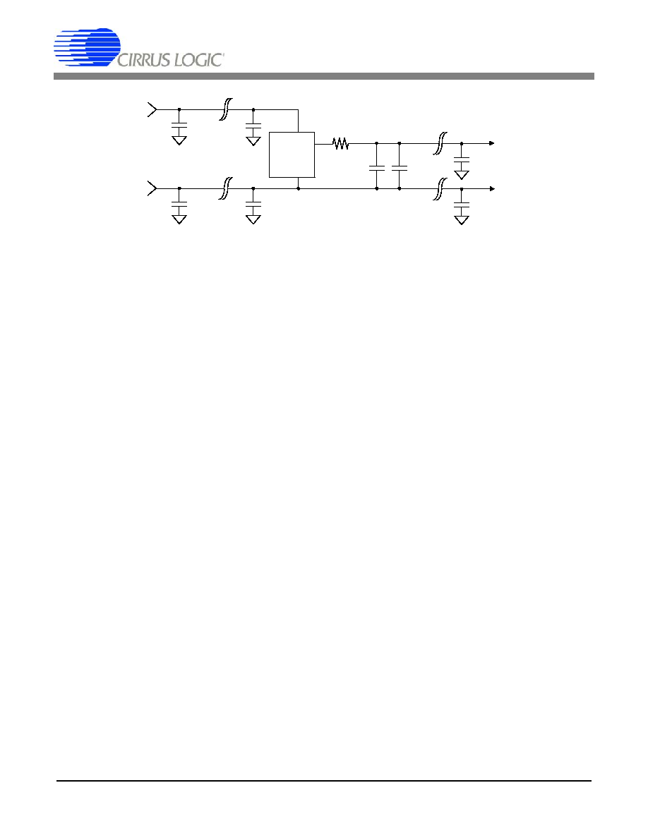
CS5373A
DS703PP2
31
8. VOLTAGE REFERENCE
The CS5373A requires a 2.500 V precision
voltage reference to be supplied to the VREF
±
pins.
8.1 VREF Power Supply
To guarantee proper regulation headroom for
the voltage reference device, the voltage refer-
ence GND pin should be connected to VA- in-
stead of system ground, as shown in
Figure 16
. This connection results in a VREF-
voltage equal to VA- and a VREF+ voltage
very near ground [(VA-) + 2.500 VREF].
Power supply inputs to the voltage reference
device should be bypassed to system ground
with 0.1
µF capacitors placed as close as pos-
sible to the power and ground pins. In addition
to 0.1
µF local bypass capacitors, at least
100
µF of bulk capacitance to system ground
should be placed on each power supply near
the voltage regulator outputs. Bypass capaci-
tors should be X7R, C0G, tantalum, or other
high-quality dielectric type.
8.2 VREF RC Filter
A primary concern in selecting a precision volt-
age reference device is noise performance in
the measurement bandwidth. The
Linear
Technology LT1019AIS8-2.5
voltage refer-
ence yields acceptable noise levels if the out-
put is filtered with a low-pass RC filter.
A separate RC filter is required for each sys-
tem device connected to a given voltage refer-
ence. By sharing a common RC filter, signal-
dependent sampling of the voltage reference
by one system device could cause unwanted
tones to appear in the measurement band-
width of another system device via common
impedance coupling.
8.3 VREF PCB Routing
To minimize the possibility of outside noise
coupling into the CS5373A voltage reference
input, the VREF
±
traces should be routed as a
differential pair from the large capacitor of the
voltage reference RC filter. Careful control of
the voltage reference source and return cur-
rents by routing VREF
±
as a differential pair
will improve immunity from external noise.
To further improve noise rejection of the
VREF
± routing,
include 0.1
µF
bypass
ca-
pacitors to system ground as close as possible
to the VREF+ and VREF- pins of the
CS5373A.
8.4 VREF Input Impedance
The switched-capacitor input architecture of
the VREF
±
inputs results in an input imped-
ance that depends on the internal capacitor
size and the clock frequency. With a 15 pF in-
ternal capacitor and a 2.048 MHz MCLK the
VREF input impedance is approximately
[1 / [(2.048 MHz) * (15 pF)]] = 32 k
. While
the size of the internal capacitor is fixed, the
voltage reference input impedance will vary
10
To VREF+
+
From VA+
Regulator
2.500 V
VREF
0.1
µF
To VREF-
0.1
µF
100
µF
0.1
µF
0.1
µF
0.1
µF
100
µF
100
µF
From VA-
Regulator
Route VREF
±
as a differential pair
from the 100uF RC filter capacitor
Figure 16. Voltage Reference Circuit

CS5373A
32
DS703PP2
with MCLK.
The voltage reference external RC filter series
resistor creates a voltage divider with the
VREF input impedance to reduce the effective
applied input voltage. To minimize gain error
resulting from this voltage divider effect, the
RC filter series resistor should be the minimum
size recommended in the voltage reference
device data sheet.
8.5 VREF Accuracy
The nominal voltage reference input is speci-
fied as 2.500 V across the VREF
±
pins, and all
CS5373A gain accuracy specifications are
measured with a nominal voltage reference in-
put. Any variation from a nominal VREF input
will proportionally vary the analog full-scale
gain accuracy.
Since temperature drift of the voltage refer-
ence results in gain drift of the analog full-scale
amplitude, care should be taken to minimize
temperature drift effects through careful selec-
tion of passive components and the voltage
reference device itself. Gain drift specifications
of the CS5373A do not include the tempera-
ture drift effects of external passive compo-
nents or of the voltage reference device itself.
8.6 VREF Independence
If the test signal source is required to be fully
independent of the measurement channel, the
CS5373A device cannot be used. Instead, a
CS5371 modulator and a CS4373A test DAC
should be used and connected to two indepen-
dent voltage reference devices. This will elimi-
nate the possibility for undetected ratiometric
errors when the same voltage reference de-
vice is used by both the test signal source and
the measurement channel.
Because modern precision voltage references
are highly reliable, requirements for separate
modulator and test DAC voltage references
should be considered carefully. In the unlikely
event of voltage reference failure independent
of other system components, the CS5373A
volts-to-codes ratio will be out of spec and
measurement channel performance will be
poor during system self-tests.
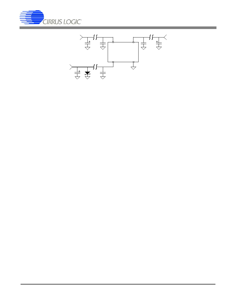
CS5373A
DS703PP2
33
9. POWER SUPPLIES
The CS5373A has a positive analog power
supply pin (VA+), a negative analog power
supply pin (VA-), a digital power supply pin
(VD), and a ground pin (GND).
For proper operation, power must be supplied
to all power supply pins, and the ground pin
must be connected to system ground. The
CS5373A digital power supply (VD) and the
CS5378 digital power supply (VDDPAD) must
share a common power supply voltage.
9.1 Power Supply Bypassing
The VA+, VA-, and VD power supplies should
be bypassed to system ground with 0.1
µF ca-
pacitors placed as close as possible to the
power pins of the device. In addition to the
0.1
µF local bypass capacitors, at least 100 µF
bulk capacitance to system ground should be
placed on each power supply near the voltage
regulator output, with additional power supply
bulk capacitance placed among the analog
component route if space permits. Bypass ca-
pacitors should be X7R, C0G, tantalum, or
other high-quality dielectric type.
9.2 PCB Layers and Routing
The CS5373A is a high-performance device,
and special care must be taken to ensure pow-
er and ground routing is correct. Power can be
supplied either through dedicated power
planes or routed traces. When routing power
traces, it is recommended to use a "star" rout-
ing scheme with the star point either at the
voltage regulator output or at a local power
supply bulk capacitor.
It is also recommended to dedicate a full PCB
layer to a solid ground plane, without splits or
routing. All bypass capacitors should connect
between the power supply circuit and the solid
ground plane as near as possible to the device
power supply pins.
The CS5373A analog signals are differentially
routed and do not normally require connection
to a separate analog ground. However, if a
separate analog ground is required, it should
be routed using a "star" routing scheme on a
separate layer from the solid ground plane and
connected to the ground plane only at the star
point. Be sure all active devices and passive
components connected to the analog ground
are included in the "star" route to ensure sen-
sitive analog currents do not return through the
ground plane.
9.3 Power Supply Rejection
Power supply rejection of the CS5373A is fre-
quency dependent. The CS5378 digital filter
rejects power supply noise for frequencies
above the selected digital filter corner frequen-
cy. Power supply noise frequencies between
DC and the digital filter corner frequency are
rejected as specified in the
Power Supply Characteristics
table.
CS5373A
VA+
VD
VA-
GND
0.1 uF
100 uF
0.1 uF
100 uF
100 uF
0.1 uF
To VA+
Regulator
To VA-
Regulator
To VD
Regulator
Figure 17. Power Supply Diagram

CS5373A
34
DS703PP2
9.4 SCR Latch-up
The VA- pin is tied to the CS5373A CMOS
substrate and must always be the most-nega-
tive voltage applied to the device to ensure
SCR latch-up does not occur. In general,
latch-up may occur when any pin voltage ex-
ceeds the limits specified in the
Absolute Maximum Ratings
table.
It is recommended to connect the VA- power
supply to system ground (GND) with a re-
verse-biased Schottky diode. At power up, if
the VA+ power supply ramps before the VA-
supply is established, the VA- pin voltage
could be pulled above ground potential
through the CS5373A device. If the VA- supply
is pulled 0.7 V or more above GND, SCR
latch-up can occur. A reverse-biased Schottky
diode will clamp the VA- voltage a maximum of
0.3 V above ground to ensure SCR latch-up
does not occur at power up.
9.5 DC-DC Converters
Many low-frequency measurement systems
are battery powered and utilize DC-DC con-
verters to efficiently generate power supply
voltages. To minimize interference effects, op-
erate the DC-DC converter at a frequency
which is rejected by the digital filter, or operate
it synchronous to the MCLK rate.
A synchronous DC-DC converter whose oper-
ating frequency is derived from MCLK will the-
oretically minimize the potential for "beat
frequencies" to appear in the
measurement
bandwidth. However this requires the source
clock to remain jitter-free within the DC-DC
converter circuitry. If clock jitter can occur with-
in the DC-DC converter (as in a PLL-based ar-
chitecture), it's better to use a non-
synchronous DC-DC converter whose switch-
ing frequency is rejected by the digital filter.
During PCB layout, do not place high-current
DC-DC converters near sensitive analog com-
ponents. Carefully routing a separate DC-DC
"star" ground will help isolate noisy switching
currents away from the sensitive analog com-
ponents.

CS5373A
DS703PP2
35
10. TERMINOLOGY
∑
Signal-to-Noise Ratio (Dynamic Range) - Ratio of the rms magnitude of the full-scale signal to the integrated
rms noise from DC to 400 Hz. The following formula is used to calculate SNR:
∑
Total Harmonic Distortion - Ratio of the power of the fundamental frequency to the sum of the powers of all
harmonic frequencies from DC to 400 Hz. The following formula is used to calculate THD:
∑
Full-scale Bandwidth - The bandwidth in which the converter can generate a full-scale signal while maintaining
performance specifications.
∑
Impulse Amplitude - The maximum amplitude of the output signal beyond the full-scale bandwidth.
∑
Differential Output Level - The voltage between the analog output pins of the device.
∑
Full-scale Accuracy - Variation in the measured output voltage from the theoretical full-scale output voltage at
1x attenuation. The following formula is used to calculate full-scale accuracy:
∑
Relative Accuracy - Variation in the measured output voltage from the theoretical attenuated output voltage at
each of the attenuation ranges. The following formula is used to calculate relative accuracy:
∑
Full Scale Drift - The variation of the measured full-scale voltage across the specified temperature range.
∑
Common Mode Drift - The variation in the measured common mode voltage across the specified temperature
range.
SNR = 20log rms magnitude of full scale signal
rms magnitude of noise floor
(
(
THD = 10log
power of the fundamental frequency
sum of the powers of the harmonic frequencies
(
(
full scale accuracy =
measured full scale voltage - theoretical full scale voltage
theoretical full scale voltage
(
(
∑100%
|
|
relative accuracy =
measured attenuated voltage - theoretical attenuated voltage
theoretical attenuated voltage (relative to the measured full scale voltage)
(
(
∑100%
|
|
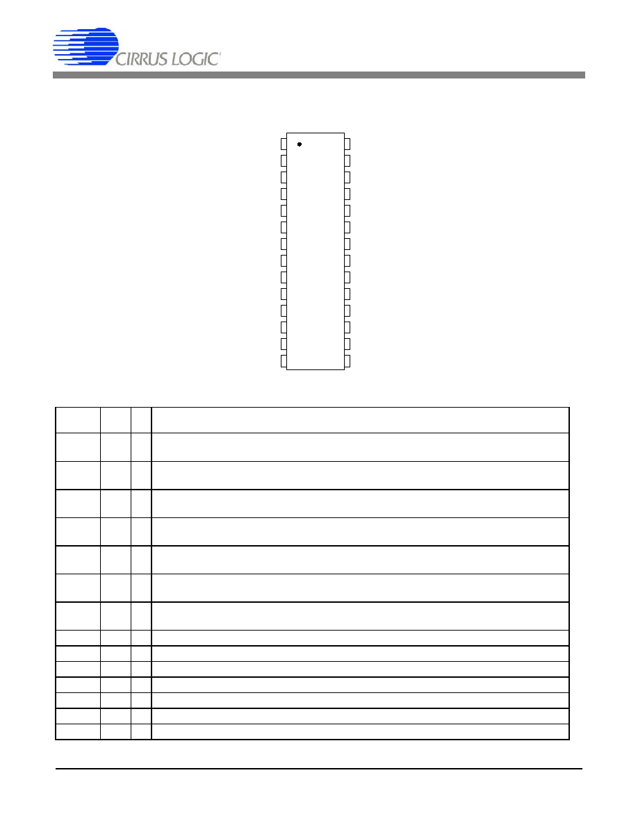
CS5373A
36
DS703PP2
11. PIN DESCRIPTION
1
2
3
4
5
6
7
8
21
22
23
24
25
26
27
28
9
10
11
12
17
18
19
20
13
14
15
16
Positive Capacitor Output
CAP+
Negative Capacitor Output
CAP-
Positive Buffered Output
BUF+
Negative Buffered Output
BUF-
Positive High Precision Output
OUT+
Negative High Precision Output
OUT-
Positive Analog Power Supply
VA+
Negative Analog Power Supply
VA-
Negative Voltage Reference
VREF-
Positive Voltage Reference
VREF+
Positive Analog Rough Input
INR+
Positive Analog Fine Input
INF+
Negative Analog Fine Input
INF-
Negative Analog Rough Input
INR-
GND
System Ground
MODE0
Mode Select
MODE1
Mode Select
MODE2
Mode Select
ATT0
Attenuation Range Select
ATT1
Attenuation Range Select
ATT2
Attenuation Range Select
TDATA
Test Bit Stream Input
VD
Positive Digital Power Supply
GND
System Ground
MCLK
Master Clock Input
MSYNC
Master Sync Input
MDATA
Modulator Data Output
MFLAG
Modulator Over-range Indicator
Pin
Name
Pin # I/O
Pin Description
CAP+,
CAP-
1
2
O
Capacitor connection for internal anti-alias filter.
BUF+,
BUF-
3
4
O
Buffered differential analog output.
OUT+,
OUT-
5
6
O
Precision differential analog output.
VA+,
VA-
7
8
Analog power supply. Refer to the Specified Operating Conditions.
VREF-,
VREF+
9
10
I Voltage reference input. Refer to the Specified Operating Conditions.
INR+,
INF+
11
12
I Analog differential rough and fine + inputs. From the + half of the differential anti-alias fil-
ter.
INF-,
INR-,
13
14
I Analog differential rough and fine - inputs. From the - half of the differential anti-alias filter.
MFLAG
15
O
Amplitude overload indicator flag.
MDATA
16
O
Oversampled
bit stream conversion output.
MSYNC
17
I
Master sync input. Low to high transition resets the internal clock phasing.
MCLK
18
I Master clock input. CMOS compatible clock input.
GND
19
System ground.
VD
20
Digital power supply. Refer to the Specified Operating Conditions.
TDATA
21
I
Test Bit Stream input from digital filter TBS generator.
CS5373A
DS703PP2
37
ATT2,
ATT1,
ATT0
22,
23,
24
I
Attenuation Range. Selects the output attenuation range.
MODE2,
MODE1,
MODE0
25,
26,
27
I
Mode Selection. Determines the operational mode of the device.
GND
28
System ground.
Pin
Name
Pin # I/O
Pin Description
Attenuation
Selection
ATT[2:0]
Attenuation
dB
0
0 0 0
1/1
0 dB
1
0 0 1
1/2
-6.02 dB
2
0 1 0
1/4
-12.04 dB
3
0 1 1
1/8
-18.06 dB
4
1 0 0
1/16
-24.08 dB
5
1 0 1
1/32
-30.10 dB
6
1 1 0
1/64
-36.12 dB
7
1 1 1
reserved
reserved
Modes of Operation
Selection MODE[2:0]
Mode Description
0
0 0 0
Modulator: enabled.
DAC: sleep.
1
0 0 1
Modulator: enabled.
DAC: AC OUT and BUF outputs.
2
0 1 0
Modulator: enabled.
DAC: AC OUT only, BUF high-z.
3
0 1 1
Modulator: enabled.
DAC: AC BUF only, OUT high-z.
4
1 0 0
Modulator: enabled.
DAC: DC common mode output.
5
1 0 1
Modulator: enabled.
DAC: DC differential output.
6
1 1 0
Modulator: enabled.
DAC: AC common mode output.
7
1 1 1
Modulator: sleep.
DAC: sleep.
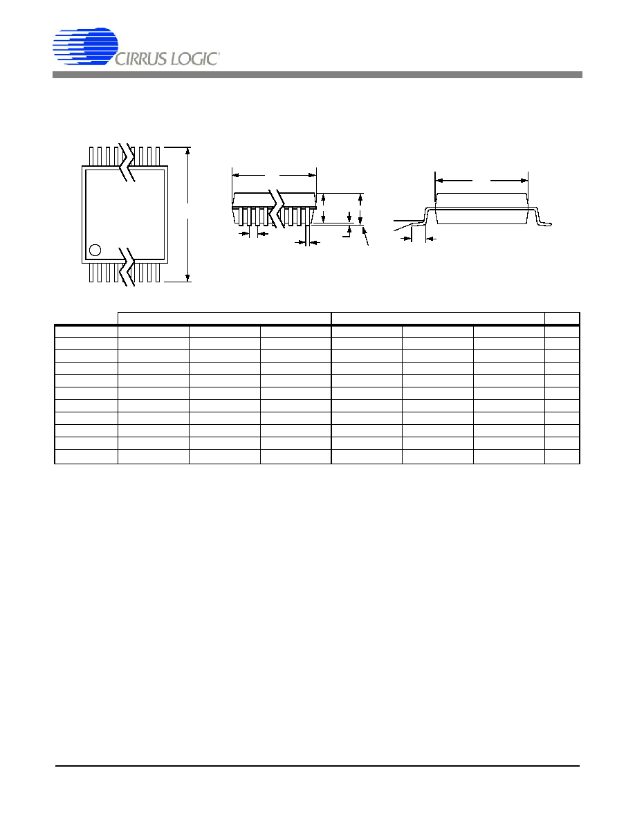
CS5373A
38
DS703PP2
12. PACKAGE DIMENSIONS
Notes: 1. "D" and "E1" are reference datums and do not included mold flash or protrusions, but do include mold
mismatch and are measured at the parting line, mold flash or protrusions shall not exceed 0.20 mm per
side.
2. Dimension "b" does not include dambar protrusion/intrusion. Allowable dambar protrusion shall be
0.13 mm total in excess of "b" dimension at maximum material condition. Dambar intrusion shall not
reduce dimension "b" by more than 0.07 mm at least material condition.
3. These dimensions apply to the flat section of the lead between 0.10 and 0.25 mm from lead tips.
INCHES
MILLIMETERS
NOTE
DIM
MIN
NOM
MAX
MIN
NOM
MAX
A
--
--
0.084
--
--
2.13
A1
0.002
0.006
0.010
0.05
0.15
0.25
A2
0.064
0.069
0.074
1.62
1.75
1.88
b
0.009
--
0.015
0.22
--
0.38
2,3
D
0.390
0.4015
0.413
9.90
10.20
10.50
1
E
0.291
0.307
0.323
7.40
7.80
8.20
E1
0.197
0.209
0.220
5.00
5.30
5.60
1
e
0.022
0.026
0.030
0.55
0.65
0.75
L
0.025
0.0354
0.041
0.63
0.90
1.03
0∞
4∞
8∞
0∞
4∞
8∞
JEDEC #: MO-150
Controlling Dimension is Millimeters
28L SSOP PACKAGE DRAWING
E
N
1 2 3
e
b
2
A1
A2
A
D
SEATING
PLANE
E1
1
L
SIDE VIEW
END VIEW
TOP VIEW
CS5373A
DS703PP2
39
13.ORDERING INFORMATION
14.ENVIRONMENTAL, MANUFACTURING, & HANDLING INFORMATION
* MSL (Moisture Sensitivity Level) as specified by IPC/JEDEC J-STD-020.
15.REVISION HISTORY
Model
Temperature
Package
CS5373A-IS
-40 to +85 ∞C
28-pin SSOP
CS5373A-ISZ (lead free)
Model Number
Peak Reflow Temp
MSL Rating*
Max Floor Life
CS5373A-IS
240 ∞C
2
365 Days
CS5373A-ISZ (lead free)
260 ∞C
3
7 Days
Revision
Date
Changes
PP1
NOV 2005
Preliminary release for CS5373A.
PP2
NOV 2005
Correct voltage units of full-scale DC differential output and common mode AC
output at 1/4 attenuation. Add T
tdata
timing to Figure 5. Correct bypass capacitor
sizes in Figure 8. Correct definition of pin 28 in Pin Description table.

CS5373A
40
DS703PP2
Contacting Cirrus Logic Support
For all product questions and inquiries contact a Cirrus Logic Sales Representative.
To find the one nearest to you go to
www.cirrus.com
IMPORTANT NOTICE
"Preliminary" product information describes products that are in production, but for which full characterization data is not yet available.
Cirrus Logic, Inc. and its subsidiaries ("Cirrus") believe that the information contained in this document is accurate and reliable. However, the information is subject
to change without notice and is provided "AS IS" without warranty of any kind (express or implied). Customers are advised to obtain the latest version of relevant
information to verify, before placing orders, that information being relied on is current and complete. All products are sold subject to the terms and conditions of sale
supplied at the time of order acknowledgment, including those pertaining to warranty, indemnification, and limitation of liability. No responsibility is assumed by Cirrus
for the use of this information, including use of this information as the basis for manufacture or sale of any items, or for infringement of patents or other rights of third
parties. This document is the property of Cirrus and by furnishing this information, Cirrus grants no license, express or implied under any patents, mask work rights,
copyrights, trademarks, trade secrets or other intellectual property rights. Cirrus owns the copyrights associated with the information contained herein and gives con-
sent for copies to be made of the information only for use within your organization with respect to Cirrus integrated circuits or other products of Cirrus. This consent
does not extend to other copying such as copying for general distribution, advertising or promotional purposes, or for creating any work for resale.
CERTAIN APPLICATIONS USING SEMICONDUCTOR PRODUCTS MAY INVOLVE POTENTIAL RISKS OF DEATH, PERSONAL INJURY, OR SEVERE PROP-
ERTY OR ENVIRONMENTAL DAMAGE ("CRITICAL APPLICATIONS"). CIRRUS PRODUCTS ARE NOT DESIGNED, AUTHORIZED OR WARRANTED FOR USE
IN AIRCRAFT SYSTEMS, MILITARY APPLICATIONS, PRODUCTS SURGICALLY IMPLANTED INTO THE BODY, AUTOMOTIVE SAFETY OR SECURITY DE-
VICES, LIFE SUPPORT PRODUCTS OR OTHER CRITICAL APPLICATIONS. INCLUSION OF CIRRUS PRODUCTS IN SUCH APPLICATIONS IS UNDERSTOOD
TO BE FULLY AT THE CUSTOMER'S RISK AND CIRRUS DISCLAIMS AND MAKES NO WARRANTY, EXPRESS, STATUTORY OR IMPLIED, INCLUDING THE
IMPLIED WARRANTIES OF MERCHANTABILITY AND FITNESS FOR PARTICULAR PURPOSE, WITH REGARD TO ANY CIRRUS PRODUCT THAT IS USED
IN SUCH A MANNER. IF THE CUSTOMER OR CUSTOMER'S CUSTOMER USES OR PERMITS THE USE OF CIRRUS PRODUCTS IN CRITICAL APPLICA-
TIONS, CUSTOMER AGREES, BY SUCH USE, TO FULLY INDEMNIFY CIRRUS, ITS OFFICERS, DIRECTORS, EMPLOYEES, DISTRIBUTORS AND OTHER
AGENTS FROM ANY AND ALL LIABILITY, INCLUDING ATTORNEYS' FEES AND COSTS, THAT MAY RESULT FROM OR ARISE IN CONNECTION WITH
THESE USES.
Cirrus Logic, Cirrus, and the Cirrus Logic logo designs are trademarks of Cirrus Logic, Inc. All other brand and product names in this document may be trademarks
or service marks of their respective owners.