1
Copyright
�
Cirrus Logic, Inc. 2004
(All Rights Reserved)
http://www.cirrus.com
CS5376A
Low Power Multi-Channel Decimation Filter
Features
1 to 4 Channel Digital Decimation Filter
Multiple On-Chip FIR and IIR Coefficient Sets
Programmable Coefficients for Custom Filters
Synchronous Operation
Selectable Output Word Rate
4000, 2000, 1000, 500, 333, 250 SPS
200, 125, 100, 50, 40, 25, 20, 10, 5, 1 SPS
Digital Gain and Offset Corrections
Test DAC Bit Stream Generator
Sine Wave or Impulse Output Mode
Time Break Controller, General Purpose I/O
Secondary SPI Port, Boundary Scan JTAG
Microcontroller or EEPROM Configuration
Small Footprint 64-pin TQFP Package
Low Power Consumption
9 mW per Channel at 500 SPS
Flexible Power Supplies
I/O Interface: 3.3 V or 5.0 V
Digital Logic Core: 3.0 V, 3.3 V or 5.0 V
Description
The CS5376A is a multi-function digital filter utilizing a
low-power signal processing architecture to achieve effi-
cient filtering for up to four
modulators. By combining
the CS5376A with CS3301/02 differential amplifiers,
CS5371/72
modulators, and the CS4373 test
DAC a synchronous high resolution multi-channel mea-
surement system can be designed quickly and easily.
Digital filter coefficients for the CS5376A FIR and IIR fil-
ters are included on-chip for a simple setup, or they can
be programmed for custom applications. Selectable dig-
ital filter decimation ratios produce output word rates
from 4000 SPS to 1 SPS, resulting in measurement
bandwidths ranging from 1600 Hz down to 400 mHz
when using the on-chip coefficient sets.
The CS5376A includes integrated peripherals to simplify
system design: offset and gain corrections, a test DAC
bit stream generator, a time break controller, 12 general
purpose I/O pins, a secondary SPI port, and a boundary
scan JTAG port.
ORDERING INFORMATION
CS5376A-IQ
-40 to +85
o
C
64-pin TQFP
I
S C K 1
S e ria l D a ta O u tp u t P o rt
D e c im a tio n a n d
F ilte rin g E n g in e
M o d u la to r D a ta
In te rfa c e
T e s t B it S tre a m C o n tr o ll e r
C lo c k a n d
S yn c h ro n iz a tio n
T B SC L K
T B SD AT A
S P I 1
S e ria l P e rip h e ra l In te rfa c e 1
J T A G
In te rfa c e
T im e B re a k C o n tr o lle r
S P I 2
S e ria l P e rip h e ra l In te rfa c e 2
G P IO
G e n e ra l P u r p o s e I/ O
SD
CL
K
SD
DA
T
SD
T
K
I
B
OOT
V
D
(
x2)
VD
D1
V
D
D
2
(
x2)
S Y N C
C L K
M C L K
M S Y N C
T IM E B
M IS O
M O S I
S S I
S IN T
SD
RD
Y
S C K 2
S O
S I1
S I2
S I3
S I4
G P IO 1 1 :E E C S
G P IO 1 0
G P IO 9
G P IO 8
G P IO 7
G P IO 6
G P IO 5
G P IO 4 :C S 4
G P IO 3 :C S 3
G P IO 2 :C S 2
G P IO 1 :C S 1
G P IO 0 :C S 0
G
ND (
x
2
)
G
N
D
2
(
x2)
GN
D
1
MD
A
T
A
[4
:1
]
M
F
L
A
G [4
:1
]
TC
K
TM
S
TD
I
TD
O
RE
SET
TR
S
T
FEB `04
DS612F1

CS5376A
2
TABLE OF CONTENTS
1. General Description. . . . . . . . . . . . . . . . . . . . . . . . . . . . . . . . . . . . . . . . 7
1.1. Digital Filter Features . . . . . . . . . . . . . . . . . . . . . . . . . . . . . . . . . . . . . . . .7
1.2. Integrated Peripheral Features . . . . . . . . . . . . . . . . . . . . . . . . . . . . . . . .8
1.3. System Level Features . . . . . . . . . . . . . . . . . . . . . . . . . . . . . . . . . . . . . .8
1.4. Configuration Interface. . . . . . . . . . . . . . . . . . . . . . . . . . . . . . . . . . . . . . .9
2. Characteristics and Specifications. . . . . . . . . . . . . . . . . . . . . . . . . . . . 13
Specified Operating Conditions . . . . . . . . . . . . . . . . . . . . . . . . . . . . . . . . . . .13
Absolute Maximum Ratings . . . . . . . . . . . . . . . . . . . . . . . . . . . . . . . . . . . . . .13
Thermal Characteristics . . . . . . . . . . . . . . . . . . . . . . . . . . . . . . . . . . . . . . . . .14
Digital Characteristics . . . . . . . . . . . . . . . . . . . . . . . . . . . . . . . . . . . . . . . . . .14
Power Consumption. . . . . . . . . . . . . . . . . . . . . . . . . . . . . . . . . . . . . . . . . . . .14
Switching Characteristics . . . . . . . . . . . . . . . . . . . . . . . . . . . . . . . . . . . . . . . .15
3. System Design with CS5376A. . . . . . . . . . . . . . . . . . . . . . . . . . . . . . . 19
3.1. Power Supplies . . . . . . . . . . . . . . . . . . . . . . . . . . . . . . . . . . . . . . . . . . .19
3.2. Reset Control . . . . . . . . . . . . . . . . . . . . . . . . . . . . . . . . . . . . . . . . . . . . .19
3.3. Clock Generation . . . . . . . . . . . . . . . . . . . . . . . . . . . . . . . . . . . . . . . . . .20
3.4. Synchronization . . . . . . . . . . . . . . . . . . . . . . . . . . . . . . . . . . . . . . . . . . .20
3.5. System Configuration. . . . . . . . . . . . . . . . . . . . . . . . . . . . . . . . . . . . . . .20
3.6. Digital Filter Operation . . . . . . . . . . . . . . . . . . . . . . . . . . . . . . . . . . . . . .20
3.7. Data Collection. . . . . . . . . . . . . . . . . . . . . . . . . . . . . . . . . . . . . . . . . . . .20
3.8. Integrated peripherals . . . . . . . . . . . . . . . . . . . . . . . . . . . . . . . . . . . . . .20
4. Power Supplies . . . . . . . . . . . . . . . . . . . . . . . . . . . . . . . . . . . . . . . . . . 21
4.1. Pin Descriptions . . . . . . . . . . . . . . . . . . . . . . . . . . . . . . . . . . . . . . . . . . .21
4.2. Bypass Capacitors . . . . . . . . . . . . . . . . . . . . . . . . . . . . . . . . . . . . . . . . .22
4.3. Power Consumption. . . . . . . . . . . . . . . . . . . . . . . . . . . . . . . . . . . . . . . .22
5. Reset Control. . . . . . . . . . . . . . . . . . . . . . . . . . . . . . . . . . . . . . . . . . . . 23
5.1. Pin Descriptions . . . . . . . . . . . . . . . . . . . . . . . . . . . . . . . . . . . . . . . . . . .23
5.2. Reset Self-Tests. . . . . . . . . . . . . . . . . . . . . . . . . . . . . . . . . . . . . . . . . . .23
5.3. Boot Configurations . . . . . . . . . . . . . . . . . . . . . . . . . . . . . . . . . . . . . . . .23
6. Clock Generation. . . . . . . . . . . . . . . . . . . . . . . . . . . . . . . . . . . . . . . . . 24
6.1. Pin Description . . . . . . . . . . . . . . . . . . . . . . . . . . . . . . . . . . . . . . . . . . . .24
6.2. Synchronous Clocking . . . . . . . . . . . . . . . . . . . . . . . . . . . . . . . . . . . . . .24
6.3. Master Clock Jitter and Skew. . . . . . . . . . . . . . . . . . . . . . . . . . . . . . . . .24
7. Synchronization . . . . . . . . . . . . . . . . . . . . . . . . . . . . . . . . . . . . . . . . . . 25
7.1. Pin Description . . . . . . . . . . . . . . . . . . . . . . . . . . . . . . . . . . . . . . . . . . . .25
7.2. MSYNC Generation . . . . . . . . . . . . . . . . . . . . . . . . . . . . . . . . . . . . . . . .25
7.3. Digital Filter Synchronization . . . . . . . . . . . . . . . . . . . . . . . . . . . . . . . . .25
7.4. Modulator Synchronization . . . . . . . . . . . . . . . . . . . . . . . . . . . . . . . . . .25
7.5. Test Bit Stream Synchronization . . . . . . . . . . . . . . . . . . . . . . . . . . . . . .25
8. Configuration By EEPROM . . . . . . . . . . . . . . . . . . . . . . . . . . . . . . . . . 26
8.1. Pin Descriptions . . . . . . . . . . . . . . . . . . . . . . . . . . . . . . . . . . . . . . . . . . .26
8.2. EEPROM Hardware Interface . . . . . . . . . . . . . . . . . . . . . . . . . . . . . . . .26
8.3. EEPROM Organization . . . . . . . . . . . . . . . . . . . . . . . . . . . . . . . . . . . . .26
8.4. EEPROM Configuration Commands . . . . . . . . . . . . . . . . . . . . . . . . . . .28
8.5. Example EEPROM Configuration . . . . . . . . . . . . . . . . . . . . . . . . . . . . .30
9. Configuration By Microcontroller . . . . . . . . . . . . . . . . . . . . . . . . . . . . . 32

CS5376A
3
9.1. Pin Descriptions . . . . . . . . . . . . . . . . . . . . . . . . . . . . . . . . . . . . . . . . . . .32
9.2. Microcontroller Hardware Interface . . . . . . . . . . . . . . . . . . . . . . . . . . . .32
9.3. Microcontroller Serial Transactions . . . . . . . . . . . . . . . . . . . . . . . . . . . .32
9.4. Microcontroller Configuration Commands . . . . . . . . . . . . . . . . . . . . . . .35
9.5. Example Microcontroller Configuration . . . . . . . . . . . . . . . . . . . . . . . . .37
10. Modulator Interface . . . . . . . . . . . . . . . . . . . . . . . . . . . . . . . . . . . . . . 39
10.1. Pin Descriptions . . . . . . . . . . . . . . . . . . . . . . . . . . . . . . . . . . . . . . . . . .39
10.2. Modulator Clock Generation . . . . . . . . . . . . . . . . . . . . . . . . . . . . . . . .39
10.3. Modulator Synchronization. . . . . . . . . . . . . . . . . . . . . . . . . . . . . . . . . .39
10.4. Modulator Data Inputs . . . . . . . . . . . . . . . . . . . . . . . . . . . . . . . . . . . . .40
10.5. Modulator Flag Inputs . . . . . . . . . . . . . . . . . . . . . . . . . . . . . . . . . . . . .40
11. Digital Filter Initialization . . . . . . . . . . . . . . . . . . . . . . . . . . . . . . . . . . 41
11.1. Filter Coefficient Selection . . . . . . . . . . . . . . . . . . . . . . . . . . . . . . . . . .41
11.2. Filter Configuration Options . . . . . . . . . . . . . . . . . . . . . . . . . . . . . . . . .41
12. SINC Filter . . . . . . . . . . . . . . . . . . . . . . . . . . . . . . . . . . . . . . . . . . . . . 43
12.1. SINC1 Filter . . . . . . . . . . . . . . . . . . . . . . . . . . . . . . . . . . . . . . . . . . . . .43
12.2. SINC2 Filter . . . . . . . . . . . . . . . . . . . . . . . . . . . . . . . . . . . . . . . . . . . . .43
12.3. SINC3 Filter . . . . . . . . . . . . . . . . . . . . . . . . . . . . . . . . . . . . . . . . . . . . .43
12.4. SINC Filter Synchronization . . . . . . . . . . . . . . . . . . . . . . . . . . . . . . . . .43
13. FIR Filter . . . . . . . . . . . . . . . . . . . . . . . . . . . . . . . . . . . . . . . . . . . . . . 47
13.1. FIR1 Filter . . . . . . . . . . . . . . . . . . . . . . . . . . . . . . . . . . . . . . . . . . . . . .47
13.2. FIR2 Filter . . . . . . . . . . . . . . . . . . . . . . . . . . . . . . . . . . . . . . . . . . . . . .47
13.3. On-Chip FIR Coefficients . . . . . . . . . . . . . . . . . . . . . . . . . . . . . . . . . . .47
13.4. Programmable FIR Coefficients . . . . . . . . . . . . . . . . . . . . . . . . . . . . . .48
13.5. FIR Filter Synchronization . . . . . . . . . . . . . . . . . . . . . . . . . . . . . . . . . .48
14. IIR Filter . . . . . . . . . . . . . . . . . . . . . . . . . . . . . . . . . . . . . . . . . . . . . . . 55
14.1. IIR Architecture . . . . . . . . . . . . . . . . . . . . . . . . . . . . . . . . . . . . . . . . . .55
14.2. IIR1 Filter . . . . . . . . . . . . . . . . . . . . . . . . . . . . . . . . . . . . . . . . . . . . . . .55
14.3. IIR2 Filter . . . . . . . . . . . . . . . . . . . . . . . . . . . . . . . . . . . . . . . . . . . . . . .55
14.4. IIR3 Filter . . . . . . . . . . . . . . . . . . . . . . . . . . . . . . . . . . . . . . . . . . . . . . .56
14.5. On-Chip IIR Coefficients . . . . . . . . . . . . . . . . . . . . . . . . . . . . . . . . . . .56
14.6. Programmable IIR Coefficients . . . . . . . . . . . . . . . . . . . . . . . . . . . . . .56
14.7. IIR Filter Synchronization . . . . . . . . . . . . . . . . . . . . . . . . . . . . . . . . . . .56
15. Gain and Offset Correction . . . . . . . . . . . . . . . . . . . . . . . . . . . . . . . . 59
15.1. Gain Correction . . . . . . . . . . . . . . . . . . . . . . . . . . . . . . . . . . . . . . . . . .59
15.2. Offset Correction . . . . . . . . . . . . . . . . . . . . . . . . . . . . . . . . . . . . . . . . .59
15.3. Offset Calibration . . . . . . . . . . . . . . . . . . . . . . . . . . . . . . . . . . . . . . . . .60
16. Serial Data Port . . . . . . . . . . . . . . . . . . . . . . . . . . . . . . . . . . . . . . . . . 61
16.1. Pin Descriptions . . . . . . . . . . . . . . . . . . . . . . . . . . . . . . . . . . . . . . . . . .61
16.2. SD Port Data Format . . . . . . . . . . . . . . . . . . . . . . . . . . . . . . . . . . . . . .61
16.3. SD Port Transactions . . . . . . . . . . . . . . . . . . . . . . . . . . . . . . . . . . . . . .62
17. Test Bit Stream Generator. . . . . . . . . . . . . . . . . . . . . . . . . . . . . . . . . 64
17.1. Pin Descriptions . . . . . . . . . . . . . . . . . . . . . . . . . . . . . . . . . . . . . . . . . .64
17.2. TBS Architecture . . . . . . . . . . . . . . . . . . . . . . . . . . . . . . . . . . . . . . . . .64
17.3. TBS Configuration . . . . . . . . . . . . . . . . . . . . . . . . . . . . . . . . . . . . . . . .64
17.4. TBS Data Source . . . . . . . . . . . . . . . . . . . . . . . . . . . . . . . . . . . . . . . . .65
17.5. TBS Sine Wave Output . . . . . . . . . . . . . . . . . . . . . . . . . . . . . . . . . . . .66
17.6. TBS Impulse Output . . . . . . . . . . . . . . . . . . . . . . . . . . . . . . . . . . . . . . .66

CS5376A
4
17.7. TBS Loopback Testing. . . . . . . . . . . . . . . . . . . . . . . . . . . . . . . . . . . . .66
17.8. TBS Synchronization . . . . . . . . . . . . . . . . . . . . . . . . . . . . . . . . . . . . . .67
18. Time Break Controller . . . . . . . . . . . . . . . . . . . . . . . . . . . . . . . . . . . . 68
18.1. Pin Description . . . . . . . . . . . . . . . . . . . . . . . . . . . . . . . . . . . . . . . . . . .68
18.2. Time Break Operation . . . . . . . . . . . . . . . . . . . . . . . . . . . . . . . . . . . . .68
18.3. Time Break Delay. . . . . . . . . . . . . . . . . . . . . . . . . . . . . . . . . . . . . . . . .68
19. General Purpose I/O . . . . . . . . . . . . . . . . . . . . . . . . . . . . . . . . . . . . . 69
19.1. Pin Descriptions . . . . . . . . . . . . . . . . . . . . . . . . . . . . . . . . . . . . . . . . . .69
19.2. GPIO Architecture . . . . . . . . . . . . . . . . . . . . . . . . . . . . . . . . . . . . . . . .69
19.3. GPIO Registers . . . . . . . . . . . . . . . . . . . . . . . . . . . . . . . . . . . . . . . . . .69
19.4. GPIO Input Mode . . . . . . . . . . . . . . . . . . . . . . . . . . . . . . . . . . . . . . . . .69
19.5. GPIO Output Mode . . . . . . . . . . . . . . . . . . . . . . . . . . . . . . . . . . . . . . .69
20. Serial Peripheral Interface 2 . . . . . . . . . . . . . . . . . . . . . . . . . . . . . . . 71
20.1. Pin Descriptions . . . . . . . . . . . . . . . . . . . . . . . . . . . . . . . . . . . . . . . . . .71
20.2. SPI 2 Architecture . . . . . . . . . . . . . . . . . . . . . . . . . . . . . . . . . . . . . . . .71
20.3. SPI 2 Registers . . . . . . . . . . . . . . . . . . . . . . . . . . . . . . . . . . . . . . . . . .71
20.4. SPI 2 Transactions. . . . . . . . . . . . . . . . . . . . . . . . . . . . . . . . . . . . . . . .73
21. Boundary Scan JTAG . . . . . . . . . . . . . . . . . . . . . . . . . . . . . . . . . . . . 76
21.1. Pin Descriptions . . . . . . . . . . . . . . . . . . . . . . . . . . . . . . . . . . . . . . . . . .76
21.2. JTAG Architecture . . . . . . . . . . . . . . . . . . . . . . . . . . . . . . . . . . . . . . . .76
22. Revision History. . . . . . . . . . . . . . . . . . . . . . . . . . . . . . . . . . . . . . . . . 79
22.1. Changes from CS5376 rev A to CS5376 rev B . . . . . . . . . . . . . . . . . .79
22.2. Changes from CS5376 rev B to CS5376A rev A . . . . . . . . . . . . . . . . .79
23. Register Summary. . . . . . . . . . . . . . . . . . . . . . . . . . . . . . . . . . . . . . . 82
23.1. SPI 1 Registers . . . . . . . . . . . . . . . . . . . . . . . . . . . . . . . . . . . . . . . . . .82
23.2. Digital Filter Registers . . . . . . . . . . . . . . . . . . . . . . . . . . . . . . . . . . . . .87
24. Pin Descriptions. . . . . . . . . . . . . . . . . . . . . . . . . . . . . . . . . . . . . . . . 103
25. Package Dimensions. . . . . . . . . . . . . . . . . . . . . . . . . . . . . . . . . . . . 106
26. Document Revisions . . . . . . . . . . . . . . . . . . . . . . . . . . . . . . . . . . . 107
LIST OF FIGURES
Figure 1. CS5376A Block Diagram . . . . . . . . . . . . . . . . . . . . . . . . . . . . . . . . . . . .7
Figure 2. Digital Filtering Stages . . . . . . . . . . . . . . . . . . . . . . . . . . . . . . . . . . . . . .8
Figure 3. FIR and IIR Coefficient Set Selection Word. . . . . . . . . . . . . . . . . . . . .11
Figure 4. MOSI Write Timing in SPI Slave Mode . . . . . . . . . . . . . . . . . . . . . . . .15
Figure 5. MISO Read Timing in SPI Slave Mode . . . . . . . . . . . . . . . . . . . . . . . .15
Figure 6. SD Port Read Timing . . . . . . . . . . . . . . . . . . . . . . . . . . . . . . . . . . . . . .16
Figure 7. SYNC, MCLK, MSYNC, MDATA Interface Timing . . . . . . . . . . . . . . .17
Figure 8. TBS Output Clock and Data Timing. . . . . . . . . . . . . . . . . . . . . . . . . . .18
Figure 9. Multi-Channel System Block Diagram . . . . . . . . . . . . . . . . . . . . . . . . .19
Figure 10. Power Supply Block Diagram . . . . . . . . . . . . . . . . . . . . . . . . . . . . . .21
Figure 11. Reset Control Block Diagram . . . . . . . . . . . . . . . . . . . . . . . . . . . . . .23
Figure 12. Clock Generation Block Diagram. . . . . . . . . . . . . . . . . . . . . . . . . . . .24
Figure 13. Synchronization Block Diagram . . . . . . . . . . . . . . . . . . . . . . . . . . . . .25
Figure 14. EEPROM Configuration Block Diagram . . . . . . . . . . . . . . . . . . . . . .26

CS5376A
5
Figure 15. SPI 1 EEPROM Read Transactions . . . . . . . . . . . . . . . . . . . . . . . . .27
Figure 16. 8 Kbyte EEPROM Memory Organization. . . . . . . . . . . . . . . . . . . . . .28
Figure 17. Serial Peripheral Interface 1 (SPI 1) Block Diagram . . . . . . . . . . . . .32
Figure 18. Microcontroller Serial Transactions . . . . . . . . . . . . . . . . . . . . . . . . . .33
Figure 19. SPI 1 Registers . . . . . . . . . . . . . . . . . . . . . . . . . . . . . . . . . . . . . . . . .34
Figure 20. Modulator Data Interface . . . . . . . . . . . . . . . . . . . . . . . . . . . . . . . . . .39
Figure 21. Digital Filter Stages . . . . . . . . . . . . . . . . . . . . . . . . . . . . . . . . . . . . . .41
Figure 22. FIR and IIR Coefficient Set Selection Word. . . . . . . . . . . . . . . . . . . .42
Figure 23. SINC Filter Block Diagram . . . . . . . . . . . . . . . . . . . . . . . . . . . . . . . . .43
Figure 24. SINC Filter Stages . . . . . . . . . . . . . . . . . . . . . . . . . . . . . . . . . . . . . . .44
Figure 25. FIR Filter Block Diagram . . . . . . . . . . . . . . . . . . . . . . . . . . . . . . . . . .47
Figure 26. FIR Filter Stages . . . . . . . . . . . . . . . . . . . . . . . . . . . . . . . . . . . . . . . .49
Figure 27. FIR1 Coefficients . . . . . . . . . . . . . . . . . . . . . . . . . . . . . . . . . . . . . . . .52
Figure 28. FIR2 Linear Phase Coefficients . . . . . . . . . . . . . . . . . . . . . . . . . . . . .53
Figure 29. FIR2 Minimum Phase Coefficients . . . . . . . . . . . . . . . . . . . . . . . . . .54
Figure 30. IIR Filter Block Diagram . . . . . . . . . . . . . . . . . . . . . . . . . . . . . . . . . . .55
Figure 31. IIR Filter Stages . . . . . . . . . . . . . . . . . . . . . . . . . . . . . . . . . . . . . . . . .57
Figure 32. Gain and Offset Correction . . . . . . . . . . . . . . . . . . . . . . . . . . . . . . . .59
Figure 33. Serial Data Port Block Diagram . . . . . . . . . . . . . . . . . . . . . . . . . . . . .61
Figure 34. SD Port Data Format . . . . . . . . . . . . . . . . . . . . . . . . . . . . . . . . . . . . .62
Figure 35. SD Port Transaction . . . . . . . . . . . . . . . . . . . . . . . . . . . . . . . . . . . . .63
Figure 36. Test Bit Stream Generator Block Diagram . . . . . . . . . . . . . . . . . . . .64
Figure 37. Time Break Block Diagram . . . . . . . . . . . . . . . . . . . . . . . . . . . . . . . .68
Figure 38. GPIO Bi-directional Structure . . . . . . . . . . . . . . . . . . . . . . . . . . . . . .69
Figure 39. Serial Peripheral Interface 2 (SPI 2) Block Diagram . . . . . . . . . . . . .71
Figure 40. SPI 2 Master Mode Transactions . . . . . . . . . . . . . . . . . . . . . . . . . . .74
Figure 41. SPI 2 Transaction Details . . . . . . . . . . . . . . . . . . . . . . . . . . . . . . . . .75
Figure 42. JTAG Block Diagram . . . . . . . . . . . . . . . . . . . . . . . . . . . . . . . . . . . . .76
Figure 43. SPI 1 Control Register SPI1CTRL . . . . . . . . . . . . . . . . . . . . . . . . . . .83
Figure 44. SPI 1 Command Register SPI1CMD . . . . . . . . . . . . . . . . . . . . . . . . .84
Figure 45. SPI 1 Data Register SPI1DAT1 . . . . . . . . . . . . . . . . . . . . . . . . . . . . .85
Figure 46. SPI 1 Data Register SPI1DAT2 . . . . . . . . . . . . . . . . . . . . . . . . . . . . .86
Figure 47. Hardware Configuration Register CONFIG . . . . . . . . . . . . . . . . . . . .88
Figure 48. GPIO Configuration Register GPCFG0 . . . . . . . . . . . . . . . . . . . . . . .89
Figure 49. GPIO Configuration Register GPCFG1 . . . . . . . . . . . . . . . . . . . . . . .90
Figure 50. SPI 2 Control Register SPI2CTRL . . . . . . . . . . . . . . . . . . . . . . . . . . .91
Figure 51. SPI 2 Command Register SPI2CMD . . . . . . . . . . . . . . . . . . . . . . . . .92
Figure 52. SPI 2 Data Register SPI2DAT . . . . . . . . . . . . . . . . . . . . . . . . . . . . . .93
Figure 53. Filter Configuration Register FILTCFG . . . . . . . . . . . . . . . . . . . . . . .94
Figure 54. Gain Correction Register GAIN1 . . . . . . . . . . . . . . . . . . . . . . . . . . . .95
Figure 55. Offset Correction Register OFFSET1 . . . . . . . . . . . . . . . . . . . . . . . .96
Figure 56. Time Break Counter Register TIMEBRK . . . . . . . . . . . . . . . . . . . . . .97
Figure 57. Test Bit Stream Configuration Register TBSCFG . . . . . . . . . . . . . . .98
Figure 58. Test Bit Stream Gain Register TBSGAIN . . . . . . . . . . . . . . . . . . . . .99
Figure 59. User Defined System Register SYSTEM1. . . . . . . . . . . . . . . . . . . .100
Figure 60. Hardware Version ID Register VERSION . . . . . . . . . . . . . . . . . . . .101
Figure 61. Self Test Result Register SELFTEST . . . . . . . . . . . . . . . . . . . . . . .102

CS5376A
6
LIST OF TABLES
Table 1. Microcontroller and EEPROM Configuration Commands . . . . . . . . . . .10
Table 2. TBS Configurations Using On-Chip Data . . . . . . . . . . . . . . . . . . . . . . .11
Table 3. SPI 1 and Digital Filter Registers . . . . . . . . . . . . . . . . . . . . . . . . . . . . .12
Table 4. Maximum EEPROM Configuration . . . . . . . . . . . . . . . . . . . . . . . . . . . .28
Table 5. EEPROM Boot Configuration Commands . . . . . . . . . . . . . . . . . . . . . .29
Table 6. Example EEPROM File. . . . . . . . . . . . . . . . . . . . . . . . . . . . . . . . . . . . .31
Table 7. Microcontroller Boot Configuration Commands . . . . . . . . . . . . . . . . . .35
Table 8. Example Microcontroller Configuration . . . . . . . . . . . . . . . . . . . . . . . . .38
Table 9. SINC Filter Configurations . . . . . . . . . . . . . . . . . . . . . . . . . . . . . . . . . .44
Table 10. SINC1 and SINC2 Filter Coefficients . . . . . . . . . . . . . . . . . . . . . . . . .45
Table 11. SINC3 Filter Coefficients. . . . . . . . . . . . . . . . . . . . . . . . . . . . . . . . . . .46
Table 12. FIR Filter Characteristics . . . . . . . . . . . . . . . . . . . . . . . . . . . . . . . . . .49
Table 13. SINC + FIR Group Delay . . . . . . . . . . . . . . . . . . . . . . . . . . . . . . . . . .50
Table 14. Minimum Phase Group Delay . . . . . . . . . . . . . . . . . . . . . . . . . . . . . . .51
Table 14. IIR Filter Characteristics . . . . . . . . . . . . . . . . . . . . . . . . . . . . . . . . . . .57
Table 15. IIR Filter Coefficients. . . . . . . . . . . . . . . . . . . . . . . . . . . . . . . . . . . . . .58
Table 16. TBS Configurations Using On-chip Data . . . . . . . . . . . . . . . . . . . . . .65
Table 17. TBS Impulse Characteristics. . . . . . . . . . . . . . . . . . . . . . . . . . . . . . . .66
Table 18. JTAG Instructions and IDCODE . . . . . . . . . . . . . . . . . . . . . . . . . . . . .77
Table 19. JTAG Scan Cell Mapping . . . . . . . . . . . . . . . . . . . . . . . . . . . . . . . . . .78

CS5376A
7
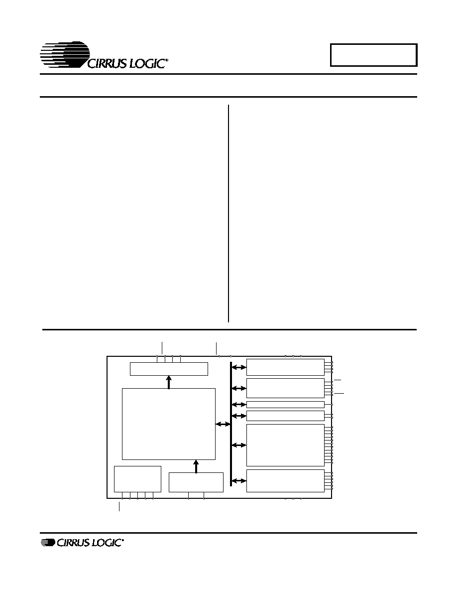
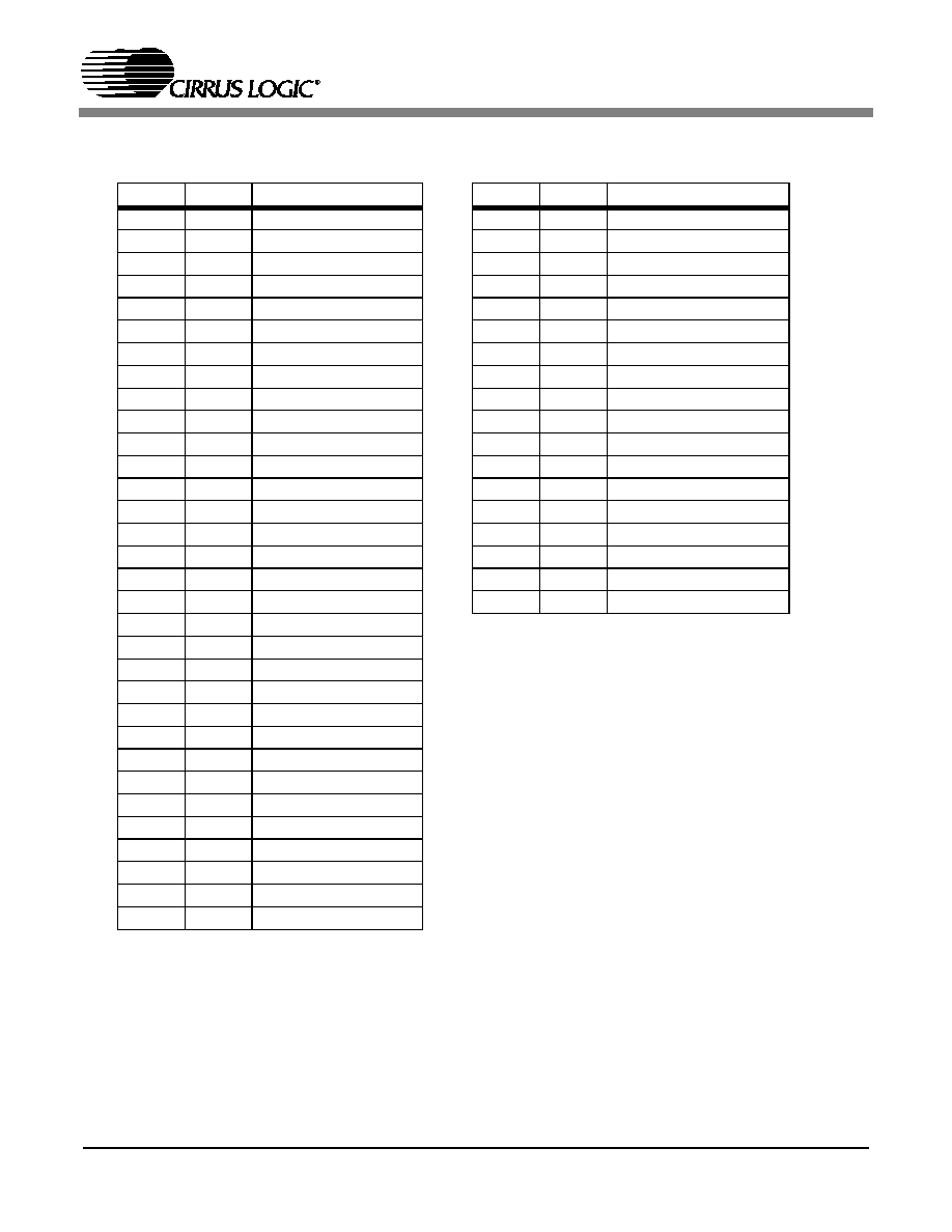
1. GENERAL DESCRIPTION
The CS5376A is a multi-channel digital filter with
integrated system peripherals. Figure 1 illustrates a
simplified block diagram of the CS5376A.
1.1 Digital Filter Features
�
Multi-channel decimation filter for CS5371/72
modulators.
-
1, 2, 3, or 4 channel concurrent operation.
�
Synchronous operation for simultaneous sam-
pling in multi-sensor systems.
-
Internal synchronization of digital filter
phase to an external SYNC signal.
�
Multiple output word rates, including low
bandwidth rates.
-
Standard output rates: 4000, 2000, 1000,
500, 333, 250 SPS.
-
Low bandwidth rates: 200, 125, 100, 50, 40,
25, 20, 10, 5, 1 SPS.
�
Flexible digital filter configuration. (See Figure
2)
-
Cascaded SINC, FIR, and IIR filters with
selectable output stage.
-
Linear and minimum phase FIR low-pass
filter coefficients included.
-
3 Hz Butterworth IIR high-pass filter coef-
ficients included.
-
FIR and IIR coefficients are programmable
to create a custom filter response.
�
Digital gain correction.
-
Individual channel gain correction to nor-
malize signal amplitudes.
Figure 1. CS5376A Block Diagram
SCK1
Serial Data Output Port
Decimation and
Filtering Engine
Modulator Data
Interface
Test Bit Stream Controller
Clock and
Synchronization
TBSCLK
TBSDATA
SPI 1
Serial Peripheral Interface 1
JTAG
Interface
Time Break Controller
SPI 2
Serial Peripheral Interface 2
GPIO
General Purpose I/O
SD
C
L
K
SD
D
A
T
SD
T
K
I
B
OOT
VD
(
x
2
)
VD
D
1
V
D
D
2
(
x2)
SYNC
CLK
MCLK
MSYNC
TIMEB
MISO
MOSI
SSI
SINT
SD
R
D
Y
SCK2
SO
SI1
SI2
SI3
SI4
GPIO11:EECS
GPIO10
GPIO9
GPIO8
GPIO7
GPIO6
GPIO5
GPIO4:CS4
GPIO3:CS3
GPIO2:CS2
GPIO1:CS1
GPIO0:CS0
G
ND (x
2
)
GN
D
2
(
x
2)
GN
D
1
M
D
AT
A [4
:
1
]
MFL
A
G
[
4
:
1
]
TC
K
TMS
TD
I
TD
O
R
E
SET
TR
S
T

CS5376A
8
�
Digital offset correction and calibration.
-
Individual channel offset correction to re-
move measurement offsets.
-
Calibration engine for automatic calcula-
tion of offset correction factors.
1.2 Integrated Peripheral Features
�
Synchronous operation for simultaneous sam-
pling in multi-sensor systems.
-
MCLK / MSYNC output signals to syn-
chronize external components.
�
High speed serial data output port (SD port).
-
Asynchronous operation to 4 MHz for di-
rect connection to system telemetry.
-
Internal 8-deep data FIFO for flexible out-
put timing.
�
Digital test bit stream signal generator suitable
for CS4373
test DAC.
-
Sine wave output mode for testing total har-
monic distortion.
-
Impulse output mode for transfer function
characterization.
-
Programmable waveform data for custom
test signal generation.
�
Time break controller to record system timing
information.
-
Dedicated TB status bit in the output data
stream.
-
Programmable output delay to match sys-
tem group delay.
�
Additional hardware peripherals simplify sys-
tem design.
-
12 General Purpose I/O (GPIO) pins for lo-
cal hardware control.
-
Secondary SPI 2 serial port to control local
serial peripherals.
-
JTAG port for boundary scan (IEEE 1149.1
compliant).
1.3 System Level Features
�
Flexible configuration options.
-
Configuration 'on-the-fly' via microcontrol-
ler or system telemetry.
-
Fixed configuration via stand-alone boot
Figure 2. Digital Filtering Stages
Sinc Filter
2 - 64000
FIR1
4
FIR2
2
IIR1
IIR2
1
st
Order
2
nd
Order
Output to High Speed Serial Data Port
DC Offset
Corrections
Output Word Rate from 4000 SPS ~ 1 SPS
Gain &
Modulator
512 kHz
Input

CS5376A
9
EEPROM.
�
Low power consumption.
-
37 mW for 4-channel operation at 500 SPS
(9.25 mW/channel).
-
40
�W standby mode.
�
Flexible power supply configurations.
-
Separate digital logic core, telemetry I/O,
and modulator I/O power supplies.
-
Telemetry I/O and modulator I/O interfaces
operate from 3.3 V or 5 V.
-
Digital logic core operates from 3.0 V,
3.3 V or 5 V.
�
Small 64-pin TQFP package.
-
Total footprint 12 mm x 12 mm plus five
bypass capacitors.
1.4 Configuration Interface
�
Configuration from microcontroller or stand-
alone boot EEPROM.
-
Microcontroller boot permits reconfigura-
tion during operation.
-
EEPROM boot sets a fixed operational con-
figuration.
�
Configuration commands written through Seri-
al Peripheral Interface 1. (See Table 1)
-
Standardized microcontroller interface us-
ing SPI 1 registers. (See Table 3)
-
Commands write digital filter registers, fil-
ter coefficients, and test bit stream data.
-
Digital filter registers set hardware config-
uration options.

CS5376A
10
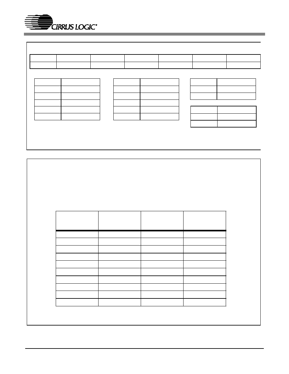
Microcontroller Boot Configuration Commands
EEPROM Boot Configuration Commands
[DATA] indicates data word returned from digital filter.
(DATA) indicates multiple words of this type are to be written.
Name
CMD
24-bit
DAT1
24-bit
DAT2
24-bit
Description
NOP
000000
-
-
No Operation
WRITE DF REGISTER
000001
REG
DATA
Write Digital Filter Register
READ DF REGISTER
000002
REG
[DATA]
-
-
Read Digital Filter Register
WRITE FIR COEFFICIENTS
000003
NUM FIR1
(FIR COEF)
NUM FIR2
(FIR COEF)
Write Custom FIR Coefficients
WRITE IIR COEFFICIENTS
000004
a11
b11
a22
b21
b10
a21
b20
b22
Write Custom IIR Coefficients
WRITE ROM COEFFICIENTS
000005
COEF SEL
-
Use On-Chip Coefficients
WRITE TBS DATA
000006
NUM TBS
(TBS DATA)
-
(TBS DATA)
Write Custom Test Bit Stream Data
WRITE ROM TBS
000007
-
-
Use On-Chip TBS Data
FILTER START
000008
-
-
Start Digital Filter Operation
FILTER STOP
000009
-
-
Stop Digital Filter Operation
Name
CMD
8-bit
DATA
24-bit
Description
NOP
00
-
No Operation
WRITE DF REGISTER
01
REG
DATA
Write Digital Filter Register
WRITE FIR COEFFICIENTS
02
NUM FIR1
NUM FIR2
(FIR COEF)
Write Custom FIR Coefficients
WRITE IIR COEFFICIENTS
03
a11
b10
b11
a21
a22
b20
b21
b22
Write Custom IIR Coefficients
WRITE ROM COEFFICIENTS
04
COEF SEL
Use On-Chip Coefficients
WRITE TBS DATA
05
NUM TBS
(TBS DATA)
Write Custom Test Bit Stream Data
WRITE ROM TBS
06
-
Use On-Chip TBS Data
FILTER START
07
-
Start Digital Filter Operation
Table 1. Microcontroller and EEPROM Configuration Commands
CS5376A
11
Bits
23:20
19:16
15:12
11:8
7:4
3:0
Selection
0000
0000
IIR2
IIR1
FIR2
FIR1
Figure 3. FIR and IIR Coefficient Set Selection Word
Bits 15:12
IIR2 Coefficients
0000
3 Hz @ 2000 SPS
0001
3 Hz @ 1000 SPS
0010
3 Hz @ 500 SPS
0011
3 Hz @ 333 SPS
0100
3 Hz @ 250 SPS
Bits 11:8
IIR1 Coefficients
0000
3 Hz @ 2000 SPS
0001
3 Hz @ 1000 SPS
0010
3 Hz @ 500 SPS
0011
3 Hz @ 333 SPS
0100
3 Hz @ 250 SPS
Bits 7:4
FIR2 Coefficients
0000
Linear Phase
0001
Minimum Phase
Bits 3:0
FIR1 Coefficients
0000
Linear Phase
0001
Minimum Phase
Test Bit Stream Characteristic Equation:
(Signal Freq) * (# TBS Data) * (Interpolation + 1) = Output Rate
Example: (31.25 Hz) * (1024) * (0x07 + 1) = 256 kHz
Signal
Frequency
(TBSDATA)
Output
Rate
(TBSCLK)
Output Rate
Selection
(RATE)
Interpolation
Selection
(INTP)
10.00 Hz
256 kHz
0x4
0x18
10.00 Hz
512 kHz
0x5
0x31
25.00 Hz
256 kHz
0x4
0x09
25.00 Hz
512 kHz
0x5
0x13
31.25 Hz
256 kHz
0x4
0x07
31.25 Hz
512 kHz
0x5
0x0F
50.00 Hz
256 kHz
0x4
0x04
50.00 Hz
512 kHz
0x5
0x09
125.00 Hz
256 kHz
0x4
0x01
125.00 Hz
512 kHz
0x5
0x03
Table 2. TBS Configurations Using On-Chip Data
CS5376A
12
SPI 1 Registers
Digital Filter Registers
Name
Addr.
Type
# Bits
Description
SPI1CTRL
00 - 02
R/W
8, 8, 8
SPI 1 Control
SPI1CMD
03 - 05
R/W
8, 8, 8
SPI 1 Command
SPI1DAT1
06 - 08
R/W
8, 8, 8
SPI 1 Data 1
SPI1DAT2
09 - 0B
R/W
8, 8, 8
SPI 1 Data 2
Name
Addr.
Type
# Bits
Description
CONFIG
00
R/W
24
Hardware Configuration
RESERVED
01-0D
R/W
24
Reserved
GPCFG0
0E
R/W
24
GPIO[7:0] Direction, Pull-up Enable, and Data
GPCFG1
0F
R/W
24
GPIO[11:8] Direction, Pull-up Enable, and Data
SPI2CTRL
10
R/W
24
SPI 2 Control
SPI2CMD
11
R/W
16
SPI 2 Command
SPI2DAT
12
R/W
24
SPI 2 Data
RESERVED
13-1F
R/W
24
Reserved
FILTCFG
20
R/W
24
Digital Filter Configuration
GAIN1
21
R/W
24
Gain Correction Channel 1
GAIN2
22
R/W
24
Gain Correction Channel 2
GAIN3
23
R/W
24
Gain Correction Channel 3
GAIN4
24
R/W
24
Gain Correction Channel 4
OFFSET1
25
R/W
24
Offset Correction Channel 1
OFFSET2
26
R/W
24
Offset Correction Channel 2
OFFSET3
27
R/W
24
Offset Correction Channel 3
OFFSET4
28
R/W
24
Offset Correction Channel 4
TIMEBRK
29
R/W
24
Time Break Delay
TBSCFG
2A
R/W
24
Test Bit Stream Configuration
TBSGAIN
2B
R/W
24
Test Bit Stream Gain
SYSTEM1
2C
R/W
24
User Defined System Register 1
SYSTEM2
2D
R/W
24
User Defined System Register 2
VERSION
2E
R/W
24
Hardware Version ID
SELFTEST
2F
R/W
24
Self-Test Result Code
Table 3. SPI 1 and Digital Filter Registers
CS5376A
13
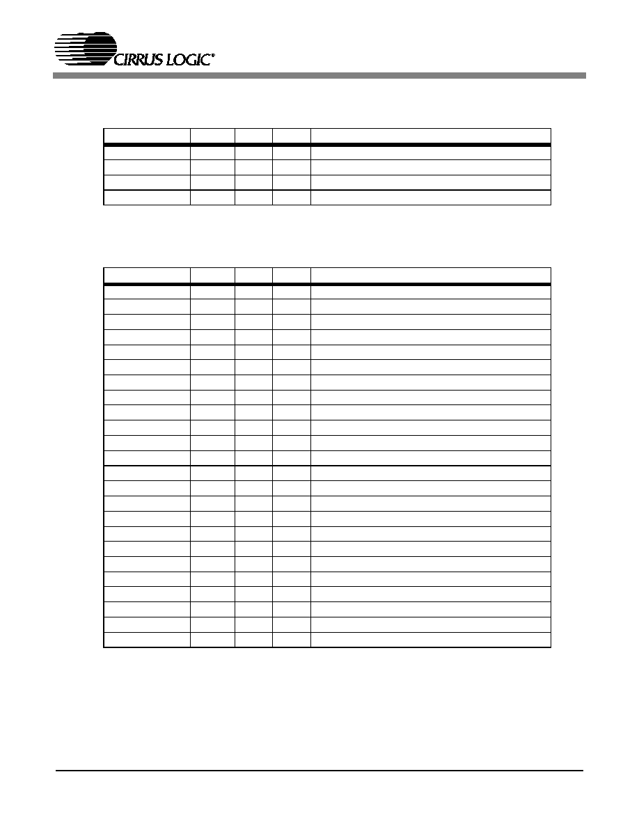
2. CHARACTERISTICS AND SPECIFICATIONS
�
Min / Max characteristics and specifications are guaranteed over the Specified Operating Conditions.
�
Typical performance characteristics and specifications are derived from measurements taken at nomi-
nal supply voltages and T
A
= 25
�C.
�
GND, GND1, GND2 = 0 V, all voltages with respect to 0 V.
SPECIFIED OPERATING CONDITIONS
ABSOLUTE MAXIMUM RATINGS
1. Transient currents up to 100 mA will not cause SCR latch-up.
Parameter
Symbol Min Nom
Max
Unit
Logic Core Power Supply
VD
2.85
3.0
5.25
V
Microcontroller Interface Power Supply
VDD1
3.135
3.3
5.25
V
Modulator Interface Power Supply
VDD2
3.135
3.3
5.25
V
Ambient Operating Temperature
Industrial (-IQ)
T
A
-40
-
85
�C
Parameter
Symbol
Min
Max
Units
DC Power Supplies
Logic Core
Microcontroller Interface
Modulator Interface
VD
VDD1
VDD2
-0.3
-0.3
-0.3
6.0
6.0
6.0
V
V
V
Input Current, Any Pin Except Supplies
(Note 1)
I
IN
-
�10
mA
Input Current, Power Supplies
(Note 1)
I
IN
-
�50
mA
Output Current
(Note 1)
I
OUT
-
�25
mA
Power Dissipation
P
DN
-
500
mW
Digital Input Voltages
V
IND
-0.3
VDD+0.3
V
Ambient Operating Temperature (Power Applied)
T
A
-40
85
�C
Storage Temperature Range
T
STG
-65
150
�C
CS5376A
14
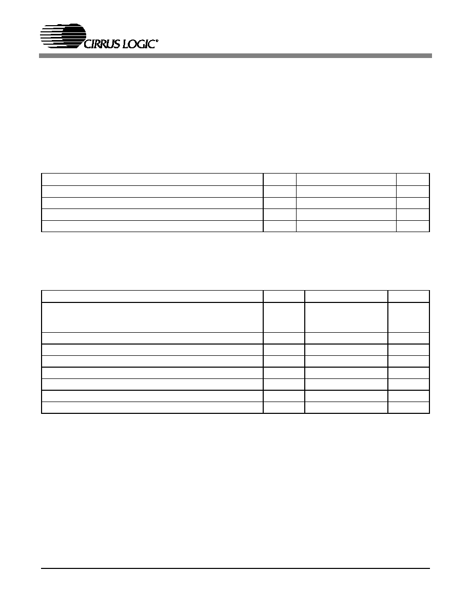
THERMAL CHARACTERISTICS
DIGITAL CHARACTERISTICS
Notes: 2. Max leakage for pins with pull-up resistors (TRST, TMS, TDI, SSI, GPIO, MOSI, SCK1) is �250
�A.
POWER CONSUMPTION
Parameter
Symbol Min Typ
Max
Unit
Allowable Junction Temperature
T
J
-
-
135
�C
Junction to Ambient Thermal Impedance
JA
-
65
�C / W
Ambient Operating Temperature (Power Applied)
T
A
-40
-
+85
�C
Parameter
Symbol Min Typ
Max
Unit
High-Level Input Drive Voltage
V
IH
0.6 * VDD
-
VDD
V
Low-Level Input Drive Voltage
V
IL
0.0
-
0.8
V
High-Level Output Drive Voltage
I
out
= -40 �A
V
OH
VDD - 0.3
-
VDD
V
Low-Level Output Drive Voltage
I
out
= +40 �A
V
OL
0.0
-
0.3
V
Rise Times, Digital Inputs
t
RISE
-
-
100
ns
Fall Times, Digital Inputs
t
FALL
-
-
100
ns
Rise Times, Digital Outputs
t
RISE
-
-
100
ns
Fall Times, Digital Outputs
t
FALL
-
-
100
ns
Input Leakage Current
(Note 2)
I
IN
-
� 1
� 10
�A
3-State Leakage Current
I
OZ
-
-
� 10
�A
Digital Input Capacitance
C
IN
-
9
-
pF
Digital Output Pin Capacitance
C
OUT
-
9
-
pF
Parameter
Symbol Min Typ
Max
Unit
Operational Power Consumption
1.024 MHz Digital Filter Clock
PWR
1
-
21
-
mW
2.048 MHz Digital Filter Clock
PWR
2
-
26
-
mW
4.096 MHz Digital Filter Clock
PWR
4
-
37
-
mW
8.192 MHz Digital Filter Clock
PWR
8
-
57
-
mW
16.384 MHz Digital Filter Clock
PWR
16
-
85
-
mW
Standby Power Consumption
32 kHz Digital Filter Clock, Filter Stopped
PWR
S
-
40
-
�W
2.6 V
0.7 V
t
fallin
t
risein
4.6 V
0.4 V
t
riseout
t
fallout
0.90 * VDD
0.10 * VDD
0.90 * VDD
0.10 * VDD

CS5376A
15
SWITCHING CHARACTERISTICS
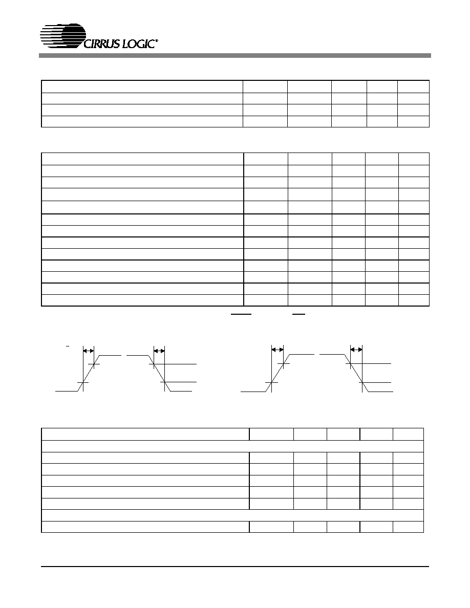
SPI 1 Interface Timing (External Master)
Parameter
Symbol Min Typ
Max
Unit
MOSI Write Timing
SSI Enable to Valid Latch Clock
t
1
60
-
-
ns
Data Set-up Time Prior to SCK1 Rising
t
2
60
-
-
ns
Data Hold Time After SCK1 Rising
t
3
120
-
-
ns
SCK1 High Time
t
4
120
-
-
ns
SCK1 Low Time
t
5
120
-
-
ns
SCK1 Falling Prior to SSI Disable
t
6
60
-
-
ns
MISO Read Timing
SCK1 Falling to New Data Bit
t
7
-
-
200
ns
SCK1 High Time
t
8
120
-
-
ns
SCK1 Low Time
t
9
120
-
-
ns
SSI Rising to MISO Hi-Z
t
10
-
-
150
ns
Figure 4. MOSI Write Timing in SPI Slave Mode
SSI
MOSI
SCLK
MSB
MSB - 1
LSB
t
6
t
5
t
4
t
3
t
2
t
1
SCK1
Figure 5. MISO Read Timing in SPI Slave Mode
MISO
SCLK
MSB
MSB - 1
LSB
t
10
t
9
t
8
t
7
SS I
SCK1
CS5376A
16
SWITCHING CHARACTERISTICS
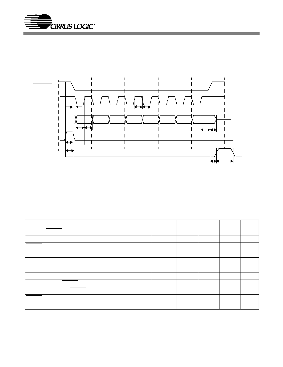
Serial Data Port (SD Port)
Parameter
Symbol Min Typ
Max
Unit
SDTKI to SDRDY Falling Edge
t
1
60
-
-
ns
SDTKI High Time Width
t
2
60
-
1000
ns
SDRDY Falling Edge to SDCLK Falling Edge
t
3
50
-
-
ns
Data Setup Time Prior to SDCLK Rising
t
4
60
-
-
ns
Data Hold Time After SDCLK Rising
t
5
60
-
-
ns
SDCLK High Time
t
6
120
-
-
ns
SDCLK Low Time
t
7
120
-
-
ns
SDCLK Rising to SDRDY Rising
t
8
60
-
-
ns
Data Hold Time After SDRDY Rising
t
9
-
-
150
ns
SDRDY High to SDTKO Rising Edge
t
10
-
-
60
ns
SDTKO High Time
t
11
90
-
-
ns
Figure 6. SD Port Read Timing
SDTKI
SDDAT
SDCLK
t
1
t
6
SDRDY
t
7
t
4
t
5
SDTKO
t
3
t
8
t
2
t
9
t
10
t
11
CS5376A
17
SWITCHING CHARACTERISTICS
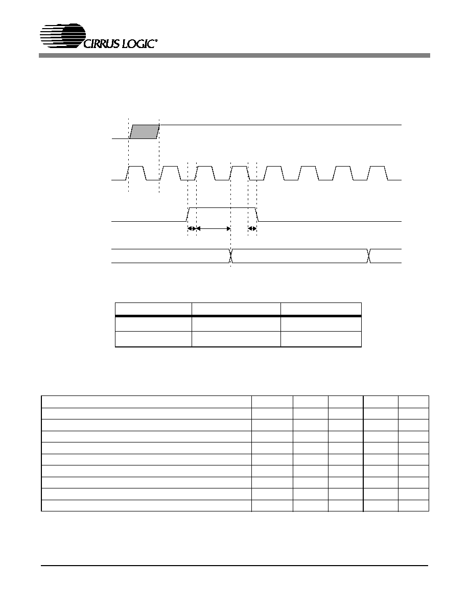
CLK, SYNC, MCLK, MSYNC, and MDATAx
Notes: 3. Master clock frequencies above or below 32.768 MHz will affect generated clock frequencies.
4. Sampling synchronization between multiple CS5376A devices receiving identical SYNC signals.
Parameter
Symbol Min Typ
Max
Unit
Master Clock Frequency
(Note 3)
CLK
32
32.768
33
MHz
Master Clock Duty Cycle
DTY
40
-
60
%
Master Clock Rise Time
t
RISE
-
-
20
ns
Master Clock Fall Time
t
FALL
-
-
20
ns
Master Clock Jitter
JTR
-
-
300
ps
Synchronization after SYNC rising
(Note 4)
SYNC
-2
-
2
�s
MSYNC Setup Time to MCLK rising
t
msr
20
-
-
ns
MCLK rising to Valid MDATA
t
mdv
-
-
75
ns
MSYNC falling to MCLK rising
t
msf
20
-
-
ns
MSYNC
MCLK
MDATAx
Figure 7. SYNC, MCLK, MSYNC, MDATA Interface Timing
t
msd
t
msd
t
msh
Data1
Data2
SYNC
f
MCLK
2.048 MHz
1.024 MHz
t
msd
= T
MCLK
/ 4
t
msd
= 122 ns
t
msd
= 244 ns
t
msh
= T
MCLK
t
msh
= 488 ns
t
msh
= 976 ns
Note: SYNC input latched on MCLK rising edge. MSYNC output triggered by MCLK falling edge.
CS5376A
18
SWITCHING CHARACTERISTICS
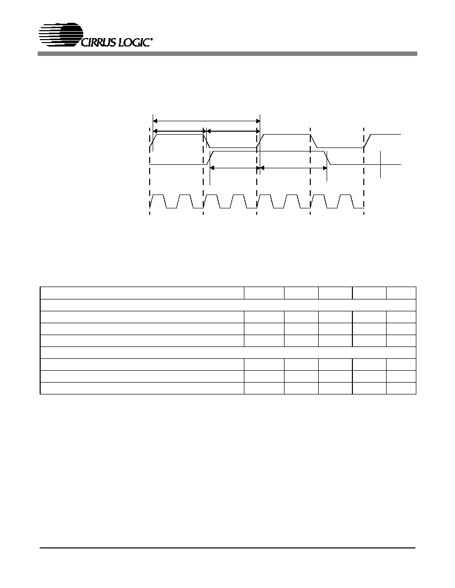
Test Bit Stream (TBS)
5. TBSCLK phase can be delayed in 1/8 increments. The timing diagram shows no TBSCLK delay.
6. TBSDATA can be delayed from 0 to 63 full bit periods. The timing diagram shows no TBSDATA delay.
Parameter
Symbol Min Typ
Max
Unit
TBS Clock Timing
TBS Clock Period
t
1
-
3.906
-
�s
TBS Clock High Time
(Note 5)
t
2
40
-
60
%
TBS Clock Low Time
t
3
40
-
60
%
TBS Data Output Timing
TBS Data Bit Rate
-
256
-
kbps
TBS Data Rising to TBS Clock Rising Setup Time
t
4
60
-
-
ns
TBS Clock Rising to TBS Data Falling Hold Time
(Note 6)
t
5
60
-
-
ns
Figure 8. TBS Output Clock and Data Timing
TBSCLK
TBSDATA
MCLK
t
1
t
2
t
3
t
5
t
4
Note: Example timing shown for a 256 kHz output rate and no programmable delays.
CS5376A
19
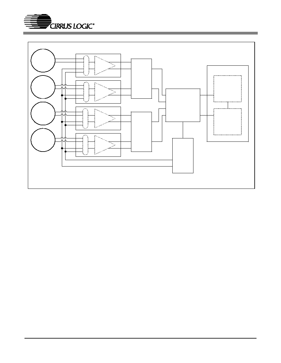
3. SYSTEM DESIGN WITH CS5376A
Figure 9 illustrates a simplified block diagram of
the CS5376A in a multi-channel measurement sys-
tem.
Up to four differential sensors are connected
through CS3301/02 differential amplifiers to the
CS5371/72
modulators, where analog to digital
conversion occurs. Each modulators 1-bit output
connects to a CS5376A MDATA input, where the
oversampled
data is decimated and filtered to
24-bit output samples at a programmed output rate.
These output samples are buffered in an 8-deep
data FIFO and passed to the system telemetry on
command.
System self tests are performed by connecting the
CS5376A test bit stream (TBS) generator to the
CS4373 test DAC. Analog tests drive differential
signals from the CS4373 test DAC into the multi-
plexed inputs of the CS3301/02 amplifiers or di-
rectly to the sensors through external analog
switches. Digital loopback tests internally connect
the TBS digital output directly to the CS5376A
modulator inputs.
3.1 Power Supplies
The multi-channel system shown in Figure 9 typi-
cally operates from a
�
2.5 V or 5 V analog power
supply and a 3.3 V digital power supply. The
CS5376A logic core can be powered from 3 V to
minimize power consumption, if required.
3.2 Reset Control
System reset is required only for the CS5376A de-
vice, and is a standard active low signal that can be
generated by a power supply monitor or microcon-
troller. Other system devices default to a power-
down state when the CS5376A is reset.
Figure 9. Multi-Channel System Block Diagram
Modulator
Modulator
Digital Filter
AMP
AMP
AMP
AMP
Geophone
or
Hydrophone
Sensor
Geophone
or
Hydrophone
Sensor
Geophone
or
Hydrophone
Sensor
Geophone
or
Hydrophone
Sensor
M
U
X
M
U
X
M
U
X
M
U
X
Test
DAC
�Controller
or
Configuration
EEPROM
Communication
Interface
CS3301
CS3302
CS5371
CS5371
CS5376A
CS4373
System Telemetry
CS3301
CS3302
CS3301
CS3302
CS3301
CS3302
CS5372
CS5372

CS5376A
20
3.3 Clock Generation
A single 32.768 MHz low-jitter clock input, which
can be generated from a VCXO based PLL, is re-
quired to drive the CS5376A device. Clock inputs
for other system devices are driven by clock out-
puts from the CS5376A.
3.4 Synchronization
Digital filter phase and analog sample timing of the
four
modulators connected to the CS5376A are
synchronized by a rising edge on the SYNC pin. If
a synchronization signal is received identically by
all CS5376A devices in a measurement network,
synchronous sampling across the network is guar-
anteed.
3.5 System Configuration
Through the SPI 1 serial port, filter coefficients and
digital filter register settings can either be pro-
grammed by a microcontroller or automatically
loaded from an external EEPROM after reset. Sys-
tem configuration is only required for the
CS5376A device, as other devices are configured
via the CS5376A General Purpose I/O pins.
Two registers in the digital filter, SYSTEM1 and
SYSTEM2 (0x2C, 0x2D), are provided for user de-
fined system information. These are general pur-
pose registers that will hold any 24-bit data values
written to them.
3.6 Digital Filter Operation
After analog to digital conversion occurs in the
modulators, the oversampled 1-bit
data is read
into the CS5376A through the MDATA pins. The
digital filter then processes data through the en-
abled filter stages, decimating it to 24-bit words at
a programmed output word rate. The final 24-bit
samples are concatenated with 8-bit status words
and placed into an output FIFO.
3.7 Data Collection
Data is collected from the CS5376A through the
Serial Data port (SD port). Automatically or upon
request, depending how the SDTKI pin is connect-
ed, the SD port initiates serial transactions to trans-
fer 32-bit data from the output FIFO to the system
telemetry. The output FIFO has eight data locations
to permit latency in data collection.
3.8 Integrated peripherals
Test Bit Stream (TBS)
A digital signal generator built into the CS5376A
produces a 1-bit
sine wave or impulse function.
This digital test bit stream can be connected to the
CS4373 test DAC to create high quality analog test
signals or it can be internally looped back to the
CS5376A MDATA inputs to test the digital filter
and data collection circuitry.
Time Break
Timing information is recorded during data collec-
tion by strobing the TIMEB pin. A dedicated flag
in the sample status bits, TB, is set high to indicate
over which measurement the timing event oc-
curred.
General Purpose I/O (GPIO)
Twelve general purpose pins are available on the
CS5376A for system control. Each pin can be set as
input or output, high or low, with an internal pull-
up enabled or disabled. The CS3301/02,
CS5371/72 and CS4373 devices in Figure 9 are
configured by simple pin settings controlled
through the CS5376A GPIO pins.
Serial Peripheral Interface 2 (SPI 2)
A secondary master mode serial port to communi-
cate with external serial peripherals.
JTAG Port
Boundary scan JTAG is IEEE 1149.1 compliant.
CS5376A
21
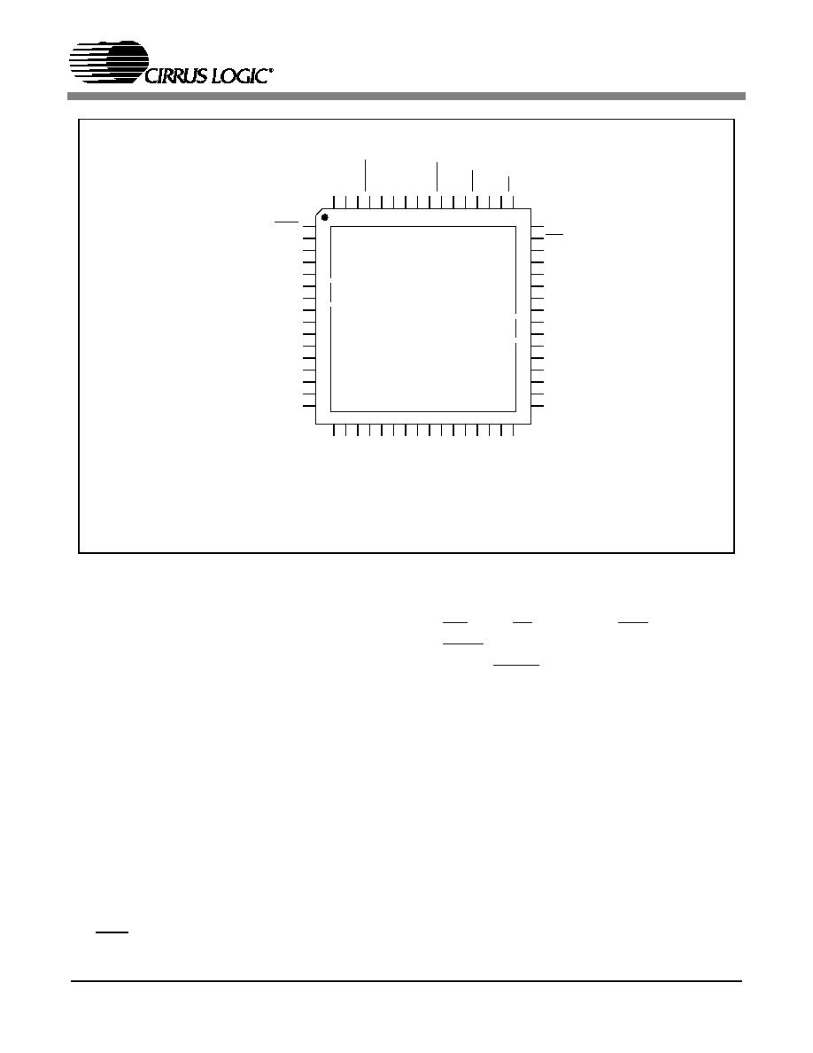
4. POWER SUPPLIES
The CS5376A has three sets of power supply in-
puts. Two sets supply power to the I/O pins of the
device (VDD1, VDD2), and the third supplies
power to the logic core (VD). The I/O pin power
supplies determine the maximum input and output
voltages when interfacing to peripherals, and the
logic core power supply largely determines the
power consumption of the CS5376A.
4.1 Pin Descriptions
VDD1, GND1 - Pins 54,53
Sets the interface voltage to a microcontroller and
system telemetry. Can be driven with voltages from
3.3 V to 5 V.
VDD1 powers pins 1-5 and 41-64:
TRST, TMS, TCK, TDI, TDO
GPIO6 - GPIO11:EECS
SSO, SCK1, SSI, MISO, MOSI, SINT,
RESET, BOOT, TIMEB, CLK, SYNC
SDDAT, SDRDY, SDCLK, SDTKO, SDTKI
VDD2, GND2 - Pins 11, 25, 24, 38
Sets the interface voltage to the modulators, test
DAC, and serial peripherals. Can be driven with
voltages from 3.3 V to 5 V.
VDD2 powers pins 8-37:
TBSCLK, TBSDATA
MCLK/2, MCLK, MSYNC
MDATA1 - MDATA4
MFLAG1 - MFLAG4
SI1 - SI4, SO, SCK2
GPIO0:CS0 - GPIO5
TRST
TMS
TCK
TDI
TDO
GND
VD
TBSCLK
TBSDATA
DNC
VDD2
MCLK/2
MCLK
MSYNC
MDATA4
MFLAG4
1
2
3
4
5
6
7
8
9
10
11
12
13
14
15
16
48
47
46
45
44
43
42
41
40
39
38
37
36
35
34
33
17 18 19 20 21 22 23 24 25 26 27 28 29 30 31 32
64 63 62 61 60 59 58 57 56 55 54 53 52 51 50 49
MD
A
T
A
3
MF
LA
G
3
MD
A
T
A
2
MF
LA
G
2
MD
A
T
A
1
MF
LA
G
1
GND
GND2
VDD2
SI
4
SI
3
SI
2
SI
1
SO
SC
K
2
GP
I
O
0
:
C
S
0
SD
T
K
I
SD
T
K
O
SD
C
L
K
SD
R
D
Y
SD
D
A
T
S
YNC
CL
K
TI
M
E
B
BO
O
T
RE
S
E
T
VDD1
GND1
SI
N
T
MO
S
I
MI
S
O
SSI
CS5376A
VDD1 Pad Ring
VDD2 Pad Ring
VD
Pad Ring
SCK1
SSO
GPIO11:EECS
GPIO10
GPIO9
GPIO8
GPIO7
GPIO6
VD
GND
GND2
GPIO5
GPIO4:CS4
GPIO3:CS3
GPIO2:CS2
GPIO1:CS1
VD
Pad Ring
Figure 10. Power Supply Block Diagram

CS5376A
22
VD, GND - Pins 7, 40, 6, 23, 39
Sets the operational voltage of the CS5376A logic
core. Can be driven with voltages from 3 V to 5 V.
A 3 V supply minimizes total power consumption.
4.2 Bypass Capacitors
Each power supply pin should be bypassed with
parallel 1
�F and 0.01 �F caps, or by a single
0.1
�F cap, placed as close as possible to the
CS5376A. Bypass capacitors should be ceramic
(X7R, C0G), tantalum, or other good quality di-
electric type.
4.3 Power Consumption
Power consumption of the CS5376A depends pri-
marily on the power supply voltage of the logic
core (VD) and the programmed digital filter clock
rate. Digital filter clock rates are selected based on
the required output word rate as explained in "Dig-
ital Filter Initialization" on page 41.
CS5376A
23
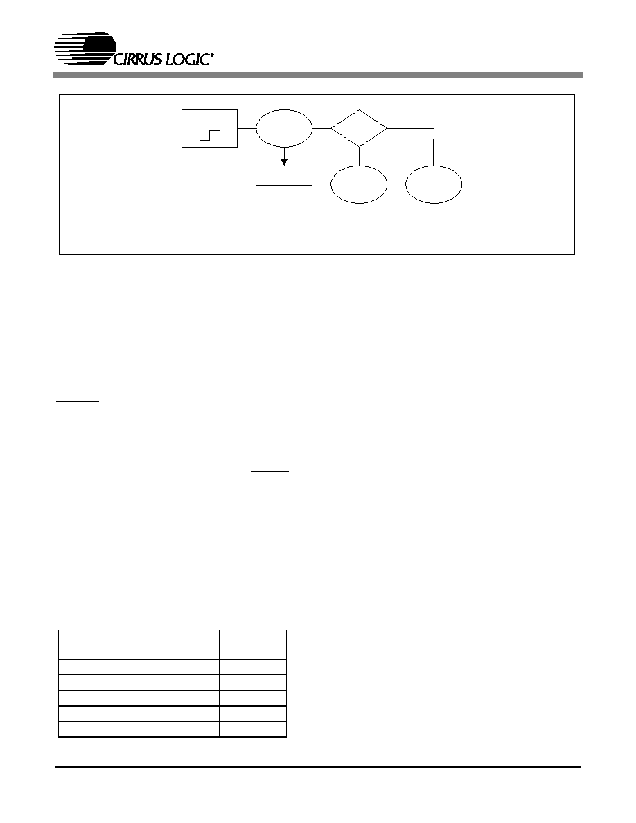
5. RESET CONTROL
The CS5376A reset signal is active low. When re-
leased, a series of self-tests are performed and the
device either actively boots from an external EE-
PROM or enters an idle state waiting for microcon-
troller configuration.
5.1 Pin Descriptions
RESET - Pin 55
Reset input, active low.
BOOT - Pin 56
Boot mode select, latched following a RESET ris-
ing edge.
BOOT = 1 = EEPROM boot
BOOT = 0 = Microcontroller boot
5.2 Reset Self-Tests
After RESET is released but before booting, a se-
ries of digital filter self-tests are run. Results are
combined into the SELFTEST register (0x2F),
with 0x0AAAAA indicating all passed. Self-tests
require 60 ms to complete, after which configura-
tion commands are serviced.
5.3 Boot Configurations
The logic state of the BOOT pin after reset deter-
mines if the CS5376A actively reads configuration
information from EEPROM or enters an idle state
waiting for a microcontroller to write configuration
commands.
EEPROM Boot
When the BOOT pin is high after reset, the
CS5376A actively reads data from an external seri-
al EEPROM and then begins operation in the spec-
ified configuration. Configuration commands and
data are encoded in the EEPROM as specified in
the `Configuration By EEPROM' section of this
data sheet, starting on page 26.
Microcontroller Boot
When the BOOT pin is low after reset, the
CS5376A enters an idle state waiting for a micro-
controller to write configuration commands and
initialize filter operation. Configuration commands
and data are written as specified in the `Configura-
tion By Microcontroller' section of this data sheet,
starting on page 32.
RESET
Self-Tests
SELFTEST
Register
BOOT
Pin
EEPROM
Boot
�Controller
Boot
1
0
Figure 11. Reset Control Block Diagram
Self-Test
Type
Pass
Code
Fail
Code
Program ROM
0x00000A
0x00000F
Data ROM
0x0000A0
0x0000F0
Program RAM
0x000A00
0x000F00
Data RAM
0x00A000
0x00F000
Execution Unit
0x0A0000
0x0F0000

CS5376A
24
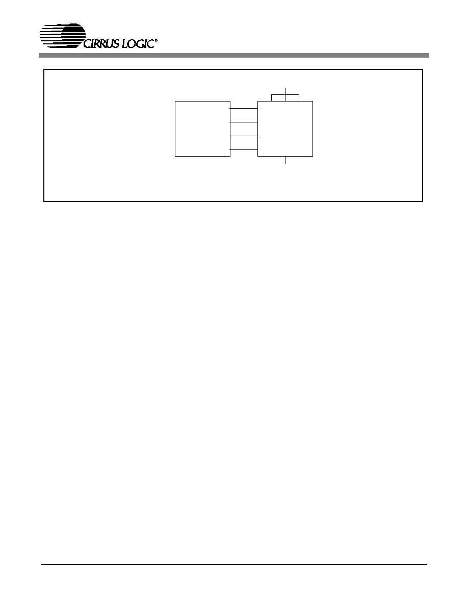
6. CLOCK GENERATION
The CS5376A requires a 32.768 MHz master clock
input, which is used to generate internal digital fil-
ter clocks and external modulator clocks.
6.1 Pin Description
CLK - Pin 58
Clock input, nominal frequency 32.768 MHz.
6.2 Synchronous Clocking
To guarantee synchronous measurements through-
out a sensor network, the CS5376A master clock
should be distributed to arrive at all nodes in phase.
The 32.768 MHz master clock can either be direct-
ly distributed through the system telemetry, or re-
constructed locally using a VCXO based PLL. To
ensure recovered clocks have identical phase, sys-
tem PLL designs should use a phase/frequency de-
tector architecture.
6.3 Master Clock Jitter and Skew
Care must be taken to minimize jitter and skew in
the received master clock as both parameters affect
measurement performance.
Jitter in the master clock causes jitter in the gener-
ated modulator clocks, resulting in sample timing
errors and increased noise.
Skew in the master clock from node to node creates
a sample timing offset, resulting in systematic mea-
surement errors in the reconstructed signal.
Clock Divider
CLK
DSPCFG Register
MCLK
Internal
Clocks
Figure 12. Clock Generation Block Diagram
and
Generator
MCLK
Output

CS5376A
25
7. SYNCHRONIZATION
The CS5376A has a dedicated SYNC input that
aligns the internal digital filter phase and generates
an external signal for synchronizing modulator an-
alog sampling. By providing simultaneous rising
edges to the SYNC pins of multiple CS5376A de-
vices, synchronous sampling across a network can
be guaranteed.
7.1 Pin Description
SYNC - Pin 59
Synchronization input, rising edge triggered.
7.2 MSYNC Generation
The SYNC signal rising edge is used to generate a
retimed synchronization signal, MSYNC. The
MSYNC signal reinitializes internal digital filter
phase and is driven onto the MSYNC output pin to
phase align modulator analog sampling.
The MSEN bit in the digital filter CONFIG register
(0x00) enables MSYNC generation. See "Modula-
tor Interface" on page 39 for more information
about MSYNC.
7.3 Digital Filter Synchronization
The internal MSYNC signal resets the digital filter
state machine to establish a known digital filter
phase. Filter convolutions restart, and the next out-
put word is available one full sample period later.
Repetitive synchronization is supported when
SYNC events occur at exactly the selected output
word rate. In this case, re-synchronization occurs at
the start of a convolution cycle when the digital fil-
ter state machine is already reset.
7.4 Modulator Synchronization
The external MSYNC signal phase aligns modula-
tor analog sampling when connected to the
CS5371/72 MSYNC input. This ensures synchro-
nous analog sampling relative to MCLK.
Repetitive synchronization of the modulators is
supported when SYNC events occur at exactly the
selected output word rate. In this case, synchroni-
zation will occur at the start of analog sampling.
7.5 Test Bit Stream Synchronization
When the test bit stream generator is enabled, an
MSYNC signal can reset the internal data pointer.
This restarts the test bit stream from the first data
point to establish a known output signal phase.
The TSYNC bit in the digital filter TBSCFG regis-
ter (0x2A) enables synchronization of the test bit
stream by MSYNC. When TSYNC is disabled, the
test bit stream phase is not affected by MSYNC.
Figure 13. Synchronization Block Diagram
SYNC
MSYNC
Digital
Filter
Generator
MSYNC
0
1
MSEN
0
1
TSYNC
Test Bit
Stream
Output
CS5376A
26
8. CONFIGURATION BY EEPROM
After reset, the CS5376A reads the state of the
BOOT pin to determine a source for configuration
commands. If BOOT is high, the CS5376A ini-
tiates serial transactions through the SPI 1 port to
read configuration information from an external
EEPROM.
8.1 Pin Descriptions
Pins required for EEPROM boot are listed here,
other SPI 1 pins are inactive.
GPIO11:EECS - Pin 46
EEPROM chip select output, active low.
SCK1 - Pin 48
Serial clock output, nominally 1.024 MHz.
MOSI - Pin 51
Serial data output pin. Valid on rising edge of
SCK1, transition on falling edge.
MISO - Pin 50
Serial data input pin. Valid on rising edge of SCK1,
transition on falling edge.
8.2 EEPROM Hardware Interface
When booting from EEPROM the CS5376A SPI 1
port actively performs serial transactions, as shown
in Figure 15, to read configuration commands and
data. 8-bit SPI opcodes and 16-bit addresses are
combined to read back 8-bit configuration com-
mands and 24-bit configuration data.
System design should include a connection to the
configuration EEPROM for in-circuit reprogram-
ming. The CS5376A SPI 1 pins tri-state when inac-
tive to support external connections to the serial
bus.
8.3 EEPROM Organization
The boot EEPROM holds the 8-bit commands and
24-bit data required to initialize the CS5376A into
an operational state. Configuration information
starts at memory location 0x10, with addresses
0x00 to 0x0F free for use as manufacturing header
information.
The first serial transaction reads a 1-byte command
from memory location 0x10 and then, depending
on the command type, reads multiple 3-byte data
words to complete the command. Command and
data reads continue until the `Filter Start' command
is recognized.
The maximum number of bytes that can be written
for a single configuration is approximately
GPIO11:EECS
SCK1
MISO
MOSI
CS5376A
AT25640
CS
SCK
SI
SO
46
48
50
51
1
6
2
5
VD
GND
WP
VCC HOLD
3
8
7
4
Figure 14. EEPROM Configuration Block Diagram

CS5376A
27
SCK1
MOSI
EECS
MSB
LSB
MISO
X
6
1
2
3
4
5
MSB
LSB
6
1
2
3
4
5
1
8
2
7
6
5
4
3
Cycle
MOSI
MISO
SSI
0x03
ADDR
DATA1
DATA3
DATA2
EECS
READ
1 BYTE / 3 BYTE
ADDR
CMD
ADDR
DATA
2 BYTE
Figure 15. SPI 1 EEPROM Read Transactions
SPI 1 Read from EEPROM
Instruction
Opcode
Address
Definition
Read
0x03
ADDR[15:0]
Read data beginning at the address given in ADDR.

CS5376A
28
5 KByte (40 Kbit), which includes command over-
head:
Supported serial configuration EEPROMs are
SPI mode 0 (0,0) compatible, 16-bit addresses, 8-
bit data, larger than 5 KByte (40 KBit). ATMEL
AT25640, AT25128, or similar serial EEPROMs
are recommended.
8.4 EEPROM Configuration Commands
A summary of available EEPROM commands is
shown in Table 5.
Write DF Register - 0x01
This EEPROM command writes a data value to the
specified digital filter register. Digital filter regis-
ters control hardware peripherals and filtering
functions. See "Digital Filter Registers" on page 87
for the bit definitions of the digital filter registers.
Sample Command:
Write digital filter register 0x00 with data value
0x070431. Then write 0x20 with data 0x000240.
01 00 00 00 07 04 31
01 00 00 20 00 02 40
Write FIR Coefficients - 0x02
This EEPROM command writes custom coeffi-
cients for the FIR1 and FIR2 filters. The first two
data words set the number of FIR1 and FIR2 coef-
ficients to be written. The remaining data words are
the concatenated FIR1 and FIR2 coefficients.
A maximum of 255 coefficients can be written for
each FIR filter, though the available digital filter
computation cycles will limit their practical size.
See "FIR Filter" on page 47 for more information
about FIR filter coefficients.
Sample Command:
Write FIR1 coefficients 0x00022E, 0x000771 then
FIR2 coefficients 0xFFFFB9, 0xFFFE8D.
02 00 00 02 00 00 02
00 02 2E 00 07 71 FF FF B9 FF FE 8D
Write IIR Coefficients - 0x03
This EEPROM command writes custom coeffi-
cients for the two stage IIR filter. The IIR architec-
ture and number of coefficients is fixed, so eight
data words containing coefficient values always
immediately follow the command byte. The IIR co-
efficient write order is: a11, b10, b11, a21, a22,
b20, b21, and b22. See "IIR Filter" on page 55 for
more information about IIR filter coefficients.
Figure 16. 8 Kbyte EEPROM Memory Organization
0000h
1FFFh
EEPROM
Manufacturing
Information
EEPROM
Command and
Data Values
Mfg Header
8-bit Command
0010h
N x 24-bit Data
8-bit Command
N x 24-bit Data
. . .
Table 4. Maximum EEPROM Configuration
Memory Requirement
Bytes
Digital Filter Registers (22)
154
FIR Coefficients (255+255)
1537
IIR Coefficients (3+5)
25
Test Bit Stream Data (1024)
3076
`Filter Start' Command
1
Total Bytes
4793

CS5376A
29
Sample Command:
Write IIR1 coefficients 0x84BC9D, 0x7DA1B1,
0x825E4F, and IIR2 coefficients 0x83694F,
0x3CAD5F, 0x3E5104, 0x835DF8, 0x3E5104.
03
84 BC 9D 7D A1 B1 82 5E 4F 83 69 4F
3C AD 5F 3E 51 04 83 5D F8 3E 51 04
Write ROM Coefficients - 0x04
This EEPROM command selects the on-chip coef-
ficients for the FIR1, FIR2, IIR 1st order, and IIR
2nd order filters for use by the digital filter. One
data word is required to select which internal coef-
ficient sets to use. See "Filter Coefficient Selec-
tion" on page 41 for information about selecting
on-chip FIR and IIR coefficient sets.
Sample Command:
Select IIR1 and IIR2 3 Hz @ 500 SPS low-cut co-
efficients, with FIR1 and FIR2 linear phase high-
cut coefficients. Data word 0x002200.
04 00 22 00
Write TBS Data - 0x05
This EEPROM command writes a custom data set
for the test bit stream (TBS) generator. This com-
mand, along with the ability to program the test bit
stream generator interpolation and clock rate, can
create custom frequency test signals.
The first data word sets the number of TBS data to
be written and the remaining data words are the
TBS data values. See "Test Bit Stream Generator"
on page 64 for information about using custom test
bit stream data sets.
Table 5. EEPROM Boot Configuration Commands
(DATA) indicates multiple words of this type are to be written.
Name
CMD
8-bit
DATA
24-bit
Description
NOP
00
-
No Operation
WRITE DF REGISTER
01
REG
DATA
Write Digital Filter Register
WRITE FIR COEFFICIENTS
02
NUM FIR1
NUM FIR2
(FIR COEF)
Write Custom FIR Coefficients
WRITE IIR COEFFICIENTS
03
a11
b10
b11
a21
a22
b20
b21
b22
Write Custom IIR Coefficients
WRITE ROM COEFFICIENTS
04
COEF SEL
Use On-Chip Coefficients
WRITE TBS DATA
05
NUM TBS
(TBS DATA)
Write Custom Test Bit Stream Data
WRITE ROM TBS
06
-
Use On-Chip TBS Data
FILTER START
07
-
Start Digital Filter Operation

CS5376A
30
Sample Command:
Write test bit stream data 0x000000, 0x0007DA,
0x000FB5, 0x00178F.
05 00 00 04
00 00 00 00 07 DA 00 0F B5 00 17 8F
Write TBS ROM Data - 0x06
This EEPROM command selects the on-chip test
bit stream (TBS) data for use by the TBS generator.
No data words are required for this EEPROM com-
mand. See "Test Bit Stream Generator" on page 64
for more information about the on-chip test bit
stream data set.
Sample Command:
06
Filter Start - 0x07
This EEPROM command initializes and starts the
digital filter. Measurement data becomes available
one full sample period after this command is re-
ceived. No data words are required for this EE-
PROM command.
Sample Command:
07
8.5 Example EEPROM Configuration
Table 6 shows an example EEPROM file for a min-
imal CS5376A configuration.
CS5376A
31
Table 6. Example EEPROM File
Addr
Data
Description
00
00
Mfg header
01
00
02
00
03
00
04
00
05
00
06
00
07
00
08
00
09
00
0A
00
0B
00
0C
00
0D
00
0E
00
0F
00
10
04
Write ROM Coefficients
11
00
12
22
13
00
14
06
Write TBS ROM Data
15
01
Write CONFIG Register
16
00
17
00
18
00
19
07
1A
04
1B
31
1C
01
Write FILTCFG Register
1D
00
1E
00
1F
20
Addr
Data
Description
20
00
21
02
22
40
23
01
Write TBSCFG Register
24
00
25
00
26
2A
27
07
28
40
29
40
2A
01
Write TBSGAIN Register
2B
00
2C
00
2D
2B
2E
04
2F
B0
30
00
31
07
Filter Start

CS5376A
32
9. CONFIGURATION BY MICROCONTROLLER
After reset, the CS5376A reads the state of the
BOOT pin to determine a source for configuration
commands. If BOOT is low, the CS5376A receives
configuration commands from a microcontroller.
9.1 Pin Descriptions
Pins required for microcontroller boot are listed
here, other SPI 1 pins are inactive.
SSI - Pin 49
Slave select input pin, active low. Serial chip select
input from a microcontroller.
SCK1 - Pin 48
Serial clock input pin. Serial clock input from mi-
crocontroller, maximum 4.096 MHz.
MOSI - Pin 51
Serial data input pin. Valid on rising edge of SCK1,
transition on falling edge.
MISO - Pin 50
Serial data output pin. Valid on rising edge of
SCK1, transition on falling edge. Open drain out-
put requiring a 10 k
pull-up resistor.
SINT - Pin 52
Serial interrupt output pin, active low. 1 uS active
low pulse output when ready for next serial trans-
action.
9.2 Microcontroller Hardware Interface
When booting from a microcontroller the
CS5376A SPI 1 port receives configuration com-
mands and configuration data through serial trans-
actions, as shown in Figure 18. 8-bit SPI opcodes
and 8-bit addresses are combined to read and write
24-bit configuration commands and data.
Microcontroller serial transactions require toggling
the SSI pin as the CS5376A chip select and writing
a serial clock to the SCK1 input. Serial data is input
to the CS5376A on the MOSI pin, and output from
the CS5376A on the MISO pin.
9.3 Microcontroller Serial Transactions
Microcontroller configuration commands are writ-
ten to the digital filter through the SPI 1 registers.
A 24-bit command and two 24-bit data words can
be written to the SPI 1 registers in any single serial
transaction. Some commands require additional
data words through additional serial transactions to
complete.
9.3.1
SPI opcodes
A microcontroller communicates with the
CS5376A SPI 1 port using standard 8-bit SPI op-
codes and an 8-bit SPI address. The standard SPI
`Read' and `Write' opcodes are listed in Figure 18.
SCK1
MISO
MOSI
Pin Logic
SPI 1
Figure 17. Serial Peripheral Interface 1 (SPI 1) Block Diagram
SINT
Command
SSI
Registers
Digital Filter
Interpreter
SPI 1

CS5376A
33
SCK1
MOSI
Figure 18. Microcontroller Serial Transactions
SSI
MSB
LSB
MISO
X
6
1
2
3
4
5
MSB
LSB
6
1
2
3
4
5
1
8
2
7
6
5
4
3
Cycle
MOSI
0x02
ADDR
Data1
MISO
MOSI
MISO
Microcontroller Write to SPI 1
Microcontroller Read from SPI 1
DataN
Data2
SSI
SSI
0x03
ADDR
Data1
DataN
Data2
Instruction
Opcode
Address
Definition
Write
0x02
ADDR[7:0]
Write SPI 1 registers beginning at the address in ADDR.
Read
0x03
ADDR[7:0]
Read SPI 1 registers beginning at the address in ADDR.

CS5376A
34
9.3.2
SPI 1 registers
The SPI 1 registers are shown in Figure 19 and are
24-bit registers mapped into an 8-bit register space
as high, mid, and low bytes. See "SPI 1 Registers"
on page 82 for the bit definitions of the SPI 1 reg-
isters.
9.3.3
SPI 1 transactions
A serial transaction to the SPI 1 registers starts with
an SPI opcode, followed by an address, and then
some number of data bytes written or read starting
at that address.
Typical serial write transactions require sending
groups of 5, 8, or 11 total bytes to the SPI1CMD or
SPI1DAT1 registers.
Example 5-byte write transaction to SPI1CMD
02 03 12 34 56
Example 5-byte write transaction to SPI1DAT1
02 06 12 34 56
Example 8-byte write transaction to SPI1CMD
02 03 12 34 56 AB CD EF
Example 8-byte write transaction to SPI1DAT1
02 06 12 34 56 AB CD EF
Example 11-byte write transaction to SPI1CMD
02 03 12 34 56 AB CD EF 65 43 21
Typical serial read transactions require groups of 3
or 5 bytes, split between writing into MOSI and
reading from MISO.
3-byte read transaction of mid-byte of SPI1CTRL
MOSI: 03 01 00
MISO: xx xx 12
5-byte read transaction of SPI1DAT1
MOSI: 03 06 00 00 00
MISO: xx xx 12 34 56
9.3.4
Multiple serial transactions
Some configuration commands require multiple se-
rial transactions to complete. There must be a small
delay between transactions for the CS5376A to
process the incoming data. Three methods can be
used to ensure the CS5376A is ready to receive the
next configuration command.
1) Delay a fixed 1 ms period to guarantee enough
time for the command to be completed.
2) Monitor the SINT pin for a 1 us active low pulse.
This pulse output occurs once the CS5376A com-
pletes processing the current command.
3) Verify the status of the E2DREQ bit by reading
the SPI1CTRL register. When low, the CS5376A is
ready for the next command.
9.3.5
Polling E2DREQ
One transaction type that can always be performed
no matter the delay from the previous configuration
command is reading E2DREQ in the mid-byte of
the SPI1CTRL register. A 3-byte read transaction.
MOSI: 03 01 00
MISO: xx xx 01 <- E2DREQ bit high
MISO: xx xx 00 <- E2DREQ bit low
Name
Addr.
Type
# Bits
Description
SPI1CTRL
00 - 02
R/W
8, 8, 8
SPI 1 Control
SPI1CMD
03 - 05
R/W
8, 8, 8
SPI 1 Command
SPI1DAT1
06 - 08
R/W
8, 8, 8
SPI 1 Data 1
SPI1DAT2
09 - 0B
R/W
8, 8, 8
SPI 1 Data 2
Figure 19. SPI 1 Registers

CS5376A
35
The E2DREQ bit reads high while a configuration
command is being processed. When low, the digital
filter is ready to receive a new configuration com-
mand.
9.4 Microcontroller Configuration
Commands
A summary of available microcontroller configura-
tion commands is listed in Table 7.
Write DF Register - 0x01
This configuration command writes a specified
digital filter register. Digital filter registers control
hardware peripherals and filtering functions. See
"Digital Filter Registers" on page 87 for the bit def-
initions of the digital filter registers.
Sample Command:
Write digital filter register 0x00 with data value
0x070431. Then write 0x20 with data 0x000240.
02 03 00 00 01 00 00 00 07 04 31
Delay 1 ms, monitor SINT, or poll E2DREQ
02 03 00 00 01 00 00 20 00 02 40
Delay 1 ms, monitor SINT, or poll E2DREQ
Read DF Register - 0x02
This command reads a specified digital filter regis-
ter. The register value is requested in the first SPI
transaction, with the register value copied to
SPI1DAT1 and read in a subsequent SPI transac-
tion.
Sample Command:
Read digital filter registers 0x00 and 0x20.
02 03 00 00 02 00 00 00
[DATA] indicates data word returned from digital filter.
(DATA) indicates multiple words of this type are to be written.
Name
CMD
24-bit
DAT1
24-bit
DAT2
24-bit
Description
NOP
000000
-
-
No Operation
WRITE DF REGISTER
000001
REG
DATA
Write Digital Filter Register
READ DF REGISTER
000002
REG
[DATA]
-
-
Read Digital Filter Register
WRITE FIR COEFFICIENTS
000003
NUM FIR1
(FIR COEF)
NUM FIR2
(FIR COEF)
Write Custom FIR Coefficients
WRITE IIR COEFFICIENTS
000004
a11
b11
a22
b21
b10
a21
b20
b22
Write Custom IIR Coefficients
WRITE ROM COEFFICIENTS
000005
COEF SEL
-
Use On-Chip Coefficients
WRITE TBS DATA
000006
NUM TBS
(TBS DATA)
-
(TBS DATA)
Write Custom Test Bit Stream Data
WRITE ROM TBS
000007
-
-
Use On-Chip TBS Data
FILTER START
000008
-
-
Start Digital Filter Operation
FILTER STOP
000009
-
-
Stop Digital Filter Operation
Table 7. Microcontroller Boot Configuration Commands

CS5376A
36
Delay 1 ms, monitor SINT, or poll E2DREQ
MOSI: 03 06 00 00 00
MISO: xx xx 07 04 31
02 03 00 00 02 00 00 20
Delay 1 ms, monitor SINT, or poll E2DREQ
MOSI: 03 06 00 00 00
MISO: xx xx 00 02 40
Write FIR Coefficients - 0x03
This command writes custom coefficients for the
FIR1 and FIR2 filters. The first two data words set
the number of FIR1 and FIR2 coefficients to be
written. The remaining data words are the concate-
nated FIR1 and FIR2 coefficients.
A maximum of 255 coefficients can be written for
each FIR filter, though the available digital filter
computation cycles will limit their practical size.
See "FIR Filter" on page 47 for more information
about FIR filter coefficients.
Sample Command:
Write FIR1 coefficients 0x00022E, 0x000771 then
FIR2 coefficients 0xFFFFB9, 0xFFFE8D.
02 03 00 00 03 00 00 02 00 00 02
Delay 1 ms, monitor SINT, or poll E2DREQ
02 06 00 02 2E 00 07 71
Delay 1 ms, monitor SINT, or poll E2DREQ
02 06 FF FF B9 FF FE 8D
Delay 1 ms, monitor SINT, or poll E2DREQ
Write IIR Coefficients - 0x04
This command writes custom coefficients for the
two stage IIR filter. The IIR architecture and num-
ber of coefficients is fixed, so eight coefficient val-
ues immediately follow this command. The IIR
coefficient write order is: a11, b10, b11, a21, a22,
b20, b21, and b22. See "IIR Filter" on page 55 for
more information about IIR filter coefficients.
Sample Command:
Write IIR1 coefficients 0x84BC9D, 0x7DA1B1,
0x825E4F, and IIR2 coefficients 0x83694F,
0x3CAD5F, 0x3E5104, 0x835DF8, 0x3E5104.
02 03 00 00 04 84 BC 9D 7D A1 B1
Delay 1 ms, monitor SINT, or poll E2DREQ
02 06 82 5E 4F 83 69 4F
Delay 1 ms, monitor SINT, or poll E2DREQ
02 06 3C AD 5F 3E 51 04
Delay 1 ms, monitor SINT, or poll E2DREQ
02 06 83 5D F8 3E 51 04
Delay 1 ms, monitor SINT, or poll E2DREQ
Write ROM Coefficients - 0x05
This configuration command selects the on-chip
coefficients for FIR1, FIR2, IIR 1st order, and IIR
2nd order filters for use by the digital filter. One
data word is required to select which internal coef-
ficient sets to use. See "Filter Coefficient Selec-
tion" on page 41 for information about selecting
on-chip FIR and IIR coefficient sets.
Sample Command:
Select IIR1 and IIR2 3 Hz @ 500 SPS low-cut co-
efficients, with FIR1 and FIR2 linear phase high-
cut coefficients. Data word 0x002200.
02 03 00 00 05 00 22 00
Delay 1 ms, monitor SINT, or poll E2DREQ
Write TBS Data - 0x06
This command writes a custom data set for the test
bit stream (TBS) generator. This command, along
with the ability to program the test bit stream gen-
erator interpolation and clock rate, can create cus-
tom frequency test signals.
The first data word sets the number of TBS data to
be written and the remaining data words are the
TBS data values. See "Test Bit Stream Generator"

CS5376A
37
on page 64 for information about using custom test
bit stream data sets.
Sample Command:
Write test bit stream data 0x000000, 0x0007DA,
0x000FB5, 0x00178F.
02 03 00 00 06 00 00 04
Delay 1 ms, monitor SINT, or poll E2DREQ
02 06 00 00 00 00 07 DA
Delay 1 ms, monitor SINT, or poll E2DREQ
02 06 00 0F B5 00 17 8F
Delay 1 ms, monitor SINT, or poll E2DREQ
Write TBS ROM Data - 0x07
This command selects the on-chip test bit stream
(TBS) data for use by the TBS generator. No data
words are required for this configuration com-
mand. See "Test Bit Stream Generator" on page 64
for information about the on-chip test bit stream
data set.
Sample Command:
02 03 00 00 07
Delay 1 ms, monitor SINT, or poll E2DREQ
Filter Start - 0x08
This command initializes and starts the digital fil-
ter. Measurement data becomes available one full
sample period after this command is issued. No
data words are required for this configuration com-
mand.
Sample Command:
02 03 00 00 08
Delay 1 ms, monitor SINT, or poll E2DREQ
Filter Stop - 0x09
This command disables the digital filter. Measure-
ment data output stops immediately after this com-
mand is issued. No data words are required for this
configuration command.
Sample Command:
02 03 00 00 09
Delay 1 ms, monitor SINT, or poll E2DREQ
9.5 Example Microcontroller
Configuration
Table 6 shows example microcontroller transac-
tions for a minimal CS5376A configuration.

CS5376A
38
Table 8. Example Microcontroller Configuration
Transaction
SPI Data
Description
01
02 03 00 00 05 00 22 00
Write ROM coefficients
02
Delay 1ms, monitor SINT, or poll E2DREQ
03
02 03 00 00 07
Write ROM TBS Data
04
Delay 1ms, monitor SINT, or poll E2DREQ
05
02 03 00 00 01 00 00 00 07 04 31
Write CONFIG Register
06
Delay 1ms, monitor SINT, or poll E2DREQ
07
02 03 00 00 01 00 00 20 00 02 40
Write FILTCFG Register
08
Delay 1ms, monitor SINT, or poll E2DREQ
09
02 03 00 00 01 00 00 2A 07 40 40
Write TBSCFG Register
10
Delay 1ms, monitor SINT, or poll E2DREQ
11
02 03 00 00 01 00 00 2B 04 B0 00
Write TBSGAIN Register
12
Delay 1ms, monitor SINT, or poll E2DREQ
13
02 03 00 00 08
Filter Start
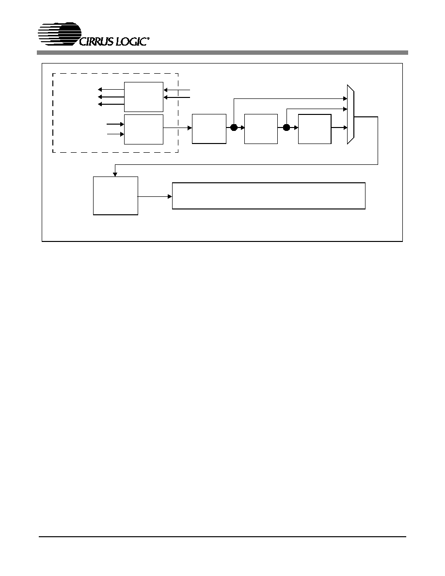
CS5376A
39
10. MODULATOR INTERFACE
The CS5376A performs digital filtering for up to
four
modulators. Signals from the modulators
are connected through the modulator data interface
(MDI).
10.1 Pin Descriptions
MCLK, MCLK/2 - Pins 13, 12
Modulator clock outputs. Nominally 2.048 MHz
and 1.024 MHz.
MSYNC - Pin 14
Modulator synchronization signal output. Generat-
ed from the SYNC input.
MDATA1 - MDATA4 - Pins 15, 17, 19, 21
Modulator data inputs, nominally 512 kbit/s.
MFLAG1 - MFLAG4 - Pins 16, 18, 20, 22
Modulator flag inputs. Driven high when modula-
tor is unstable due to an analog over-range signal.
10.2 Modulator Clock Generation
The MCLK and MCLK/2 outputs are low-jitter,
low-skew modulator clocks generated from the
32.768 MHz master clock.
MCLK typically operates at 2.048 MHz unless an-
alog low-power modes require a 1.024 MHz mod-
ulator clock. MCLK/2 always produces a clock at
half the selected MCLK rate.
The MCLK rate is selected and the MCLK and
MCLK/2 outputs are enabled by bits in the digital
filter CONFIG register (0x00). By default MCLK
and MCLK/2 are disabled and driven low.
10.3 Modulator Synchronization
The MSYNC output signal follows an input on the
SYNC pin. MSYNC phase aligns the modulator
sampling instant to guarantee synchronous analog
sampling across a measurement network.
MSYNC is enabled by a bit in the CONFIG register
(0x00). By default SYNC inputs do not cause an
MSYNC output.
Figure 20. Modulator Data Interface
FIR
IIR
Filters
Filter
Output to High Speed Serial Data Port (SD Port)
DC Offset
Correction
Output Rate 4000 SPS ~ 1 SPS
& Gain
MDATA[4:1]
MFLAG[4:1]
MDI Input
512 kHz
MCLK /
Generate
MSYNC
CLK
SYNC
MSYNC
SINC
Filter
MCLK
MCLK/2

CS5376A
40
10.4 Modulator Data Inputs
The MDATA input expects 1-bit
data at a
512 kHz or 256 kHz rate. The input rate is selected
by a bit in the CONFIG register (0x00). By default,
MDATA is expected at 512 kHz.
The MDATA input one's density is designed for
full scale positive at 86% and full scale negative at
14%, with absolute maximum over-range capabili-
ty to 93% and 7%. These raw
inputs are deci-
mated and filtered by the digital filter to create 24-
bit samples at the output rate.
10.5 Modulator Flag Inputs
A high MFLAG input signal indicates the corre-
sponding
modulator has become unstable due
to an analog over-range input signal. Once the
over-range signal is reduced, the modulator recov-
ers stability and the MFLAG signal is cleared.
The MFLAG inputs are mapped to status bits in the
SD port, and are associated with each sample when
written. See "Serial Data Port" on page 61 for more
information on the MFLAG error bits in the SD
port status byte.
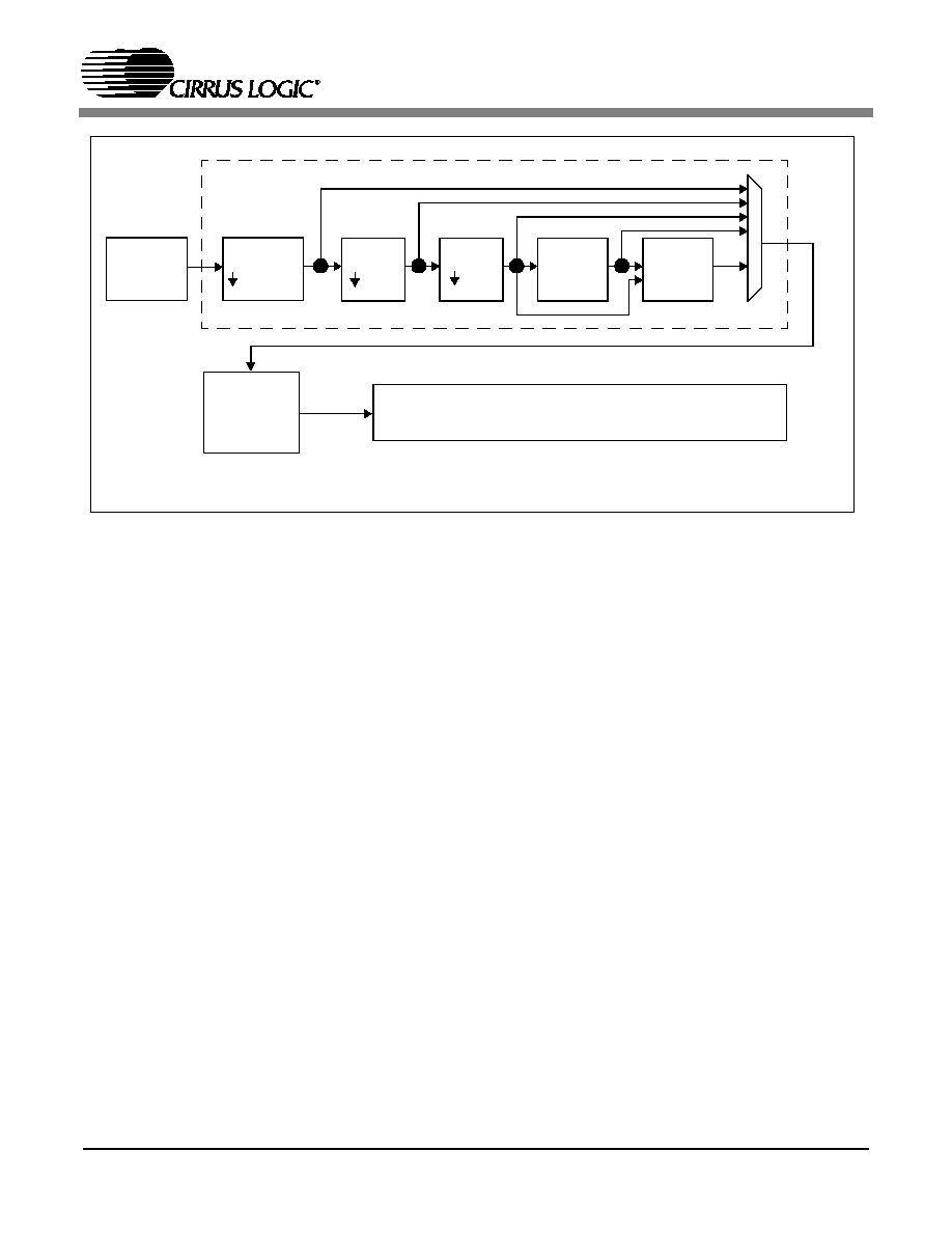
CS5376A
41
11. DIGITAL FILTER INITIALIZATION
The CS5376A digital filter consists of three multi-
stage sections: a three stage SINC filter, a two stage
FIR filter, and a two stage IIR filter.
To initialize the digital filter, FIR and IIR coeffi-
cient sets are selected using configuration com-
mands, and the FILTCFG register (0x20) is written
to select the output filter stage, the output word
rate, and the number of enabled channels. The dig-
ital filter clock rate is selected by writing the CON-
FIG register (0x00).
11.1 Filter Coefficient Selection
Selection of SINC filter coefficients is not required
as they are selected automatically based on the pro-
grammed output word rate.
Digital filter FIR and IIR coefficients are selected
using the `Write FIR Coefficients' and `Write IIR
Coefficients', or the `Write ROM Coefficients'
configuration commands. When writing the FIR
and IIR coefficients from ROM, a data word selects
an on-chip coefficient set for each filter stage. Fig-
ure 22 shows the format of the coefficient selection
word, and the available coefficient sets for each se-
lection.
Characteristics of the on-chip digital filter coeffi-
cients are discussed in the `SINC Filter', `FIR Fil-
ter', and `IIR Filter' sections of this data sheet.
11.2 Filter Configuration Options
Digital filter parameters are selected by bits in the
FILTCFG register (0x20), and the digital filter
clock rate is selected by bits in the CONFIG regis-
ter (0x00).
11.2.1 Output Filter Stage
The digital filter can output data following any
stage in the filter chain. The output filter stage is se-
lected by the FSEL bits in the FILTCFG register.
Taking data from the SINC or FIR1 filter stages re-
duces the overall decimation of the filter chain and
increases the output rate, as discussed in the fol-
lowing section. Taking data from FIR2, IIR1, IIR2,
or IIR3 results in data at the selected rate.
Figure 21. Digital Filter Stages
SINC Filter
2 - 64000
FIR1
4
FIR2
2
IIR1
IIR2
1st Order
2nd Order
Output to High Speed Serial Data Port (SD Port)
DC Offset
Correction
Output Rate 4000 SPS ~ 1 SPS
& Gain
Modulator
512 kHz
Input

CS5376A
42
11.2.2 Output Word Rate
The CS5376A digital filter supports output word
rates (OWRs) between 4000 SPS and 1 SPS. The
output word rate is selected by the DEC bits in the
FILTCFG register.
When taking data directly from the SINC filter, the
decimation of the FIR1 and FIR2 stages is by-
passed and the actual output word rate is multiplied
by a factor of eight compared with the register se-
lection. When taking data directly from FIR1, the
decimation of the FIR2 stage is bypassed and the
actual output word rate is multiplied by a factor of
two. Data taken from the FIR2, IIR1, IIR2, or IIR3
filtering stages is output at the selected rate.
11.2.3 Channel Enable
Digital filtering can be performed simultaneously
for up to four
modulators. The number of en-
abled channels is selected by the CH bits in the
FILTCFG register.
Channels are enabled sequentially. Selecting one
channel operation enables channel 1 only, selecting
two channel operation enables channels 1 and 2, se-
lecting three channel operation enables channels 1,
2, and 3, and selecting four channel operation en-
ables all four channels.
11.2.4 Digital Filter Clock
The digital filter clock rate is programmable be-
tween 16.384 MHz and 32 kHz by bits in the CON-
FIG register.
Computation Cycles
The minimum digital filter clock rate for a config-
uration depends on the computation cycles required
to complete digital filter convolutions at the select-
ed output word rate. All configurations work for a
maximum digital filter clock, but lower clock rates
consume less power.
Standby Mode
The CS5376A can be placed in a low-power stand-
by mode by sending the `Filter Stop' configuration
command and programming the digital filter clock
to 32 kHz. In this mode the digital filter idles, con-
suming minimal power until re-enabled by later
configuration commands.
Bits
23:20
19:16
15:12
11:8
7:4
3:0
Selection
0000
0000
IIR2
IIR1
FIR2
FIR1
Figure 22. FIR and IIR Coefficient Set Selection Word
Bits 15:12
IIR2 Coefficients
0000
3 Hz @ 2000 SPS
0001
3 Hz @ 1000 SPS
0010
3 Hz @ 500 SPS
0011
3 Hz @ 333 SPS
0100
3 Hz @ 250 SPS
Bits 11:8
IIR1 Coefficients
0000
3 Hz @ 2000 SPS
0001
3 Hz @ 1000 SPS
0010
3 Hz @ 500 SPS
0011
3 Hz @ 333 SPS
0100
3 Hz @ 250 SPS
Bits 7:4
FIR2 Coefficients
0000
Linear Phase
0001
Minimum Phase
Bits 3:0
FIR1 Coefficients
0000
Linear Phase
0001
Minimum Phase
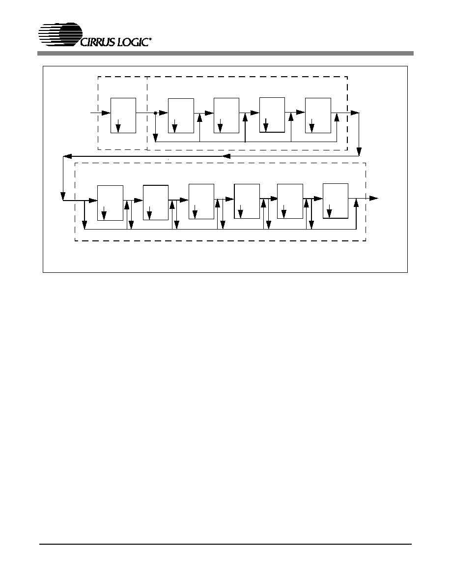
CS5376A
43
12. SINC FILTER
The SINC filters primary purpose is to attenuate
out-of-band noise components from the
modu-
lators. While doing so, they decimate 1-bit
data
into lower frequency 24-bit data suitable for the
FIR and IIR filters.
The SINC filter has three cascaded sections,
SINC1, SINC2, and SINC3, which are each made
up of the smaller stages shown in Figure 23.
The selected output word rate in the FILTCFG reg-
ister automatically determines the coefficients and
decimation ratios selected for the SINC filters.
Once the SINC filter configuration is set, all en-
abled channels are filtered and decimated using an
identical hardware algorithm.
12.1 SINC1 Filter
The first section is SINC1, a single stage 5th order
fixed decimate by 8 SINC filter. This SINC filter
decimates the incoming 1-bit
bit stream from
the modulators down to a 64 kHz rate.
12.2 SINC2 Filter
The second section is SINC2, a multi-stage, vari-
able order, variable decimation SINC filter. De-
pending on the selected output word rate in the
FILTCFG register, different cascaded SINC2 stag-
es are enabled, as shown in Table 9.
12.3 SINC3 Filter
The last section is SINC3, a flexible multi-stage
variable order, variable decimation SINC filter.
Depending on the selected output word rate in the
FILTCFG register, different SINC3 stages are en-
abled, as shown in Table 9.
12.4 SINC Filter Synchronization
The SINC filter is synchronized to the external sys-
tem by the MSYNC signal, which is generated
from the SYNC input. The MSYNC signal sets a
reference time (time 0) for all filter operations, and
the SINC filter is restarted to phase align with this
reference time.
sinc1
8
5th order
4th order
Figure 23. SINC Filter Block Diagram
1-bit
24-bit
-
2
stage1
sinc2
4th order
2
stage2
sinc2
4th order
2
stage3
sinc2
4th order
2
stage4
sinc2
4th order
5
stage1
sinc3
4th order
5
stage2
sinc3
4th order
5
stage3
sinc3
5th order
2
stage4
sinc3
6th order
2
stage5
sinc3
6th order
3
stage6
sinc3
Output
Input

CS5376A
44
SINC1 � Single stage, fixed decimate by 8
5
th
order decimate by 8, 36 coefficients
SINC2 � Multi-stage, variable decimation
Stage 1: 4
th
order decimate by 2, 5 coefficients
Stage 2: 4
th
order decimate by 2, 5 coefficients
Stage 3: 5
th
order decimate by 2, 6 coefficients
Stage 4: 6
th
order decimate by 2, 7 coefficients
SINC3 � Multi-stage, variable decimation
Stage 1: 4
th
order decimate by 5, 17 coefficients
Stage 2: 4
th
order decimate by 5, 17 coefficients
Stage 3: 4
th
order decimate by 5, 17 coefficients
Stage 4: 5
th
order decimate by 2, 6 coefficients
Stage 5: 6
th
order decimate by 2, 7 coefficients
Stage 6: 6
th
order decimate by 3, 13 coefficients
Figure 24. SINC Filter Stages
SINC filters
FIR2
Output
Word
Rate
DEC Bit
Setting
SINC1
Deci-
mation
SINC2
Deci-
mation
SINC2
Stages
SINC3
Deci-
mation
SINC3
Stages
4000
0111
8 2 4 - -
2000 0110
8
4
3,4
-
-
1000 0101
8
8
2,3,4 -
-
500 0100 8
16
1,2,3,4 -
-
333 0011 8
8 2,3,4 3
6
250 0010 8
16
1,2,3,4 2
5
200 0001 8
2
4
20 3,4,5
125 0000 8
16
1,2,3,4 4
4,5
100 1111 8
4
3,4 20 3,4,5
50 1110 8
8 2,3,4 20 3,4,5
40 1101 8
2
4 100
2,3,4,5
25 1100
8
16 1,2,3,4 20
3,4,5
20 1011 8
4
3,4 100
2,3,4,5
10 1010 8
8 2,3,4
100
2,3,4,5
5 1001 8 16
1,2,3,4
100
2,3,4,5
1 1000 8 16
1,2,3,4
500
1,2,3,4,5
Table 9. SINC Filter Configurations
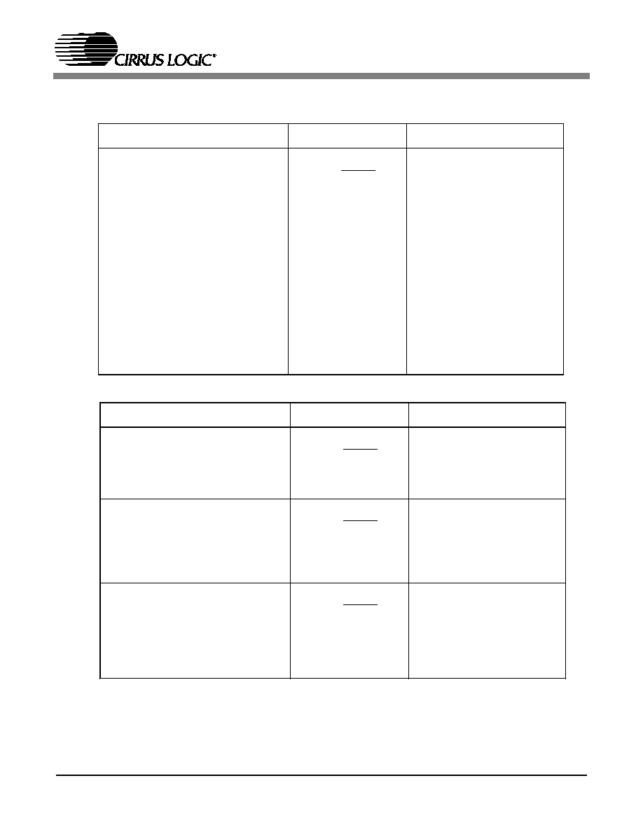
CS5376A
45
Filter Type
System Function
Filter Coefficients
SINC2 (Stage 1)
SINC2 (Stage 2)
4
th
order decimate by 2
5 coefficients
4
1
2
1
1
)
(
-
-
=
-
-
z
z
z
H
h
0
= 1
h
1
= 4
h
2
= 6
h
3
= 4
h
4
= 1
SINC2 (Stage 3)
5
th
order decimate by 2
6 coefficients
5
1
2
1
1
)
(
-
-
=
-
-
z
z
z
H
h
0
= 1
h
1
= 5
h
2
= 10
h
3
= 10
h
4
= 5
h
5
= 1
SINC2 (Stage 4)
6
th
order decimate by 2
7 coefficients
6
1
2
1
1
)
(
-
-
=
-
-
z
z
z
H
h
0
= 1
h
1
= 6
h
2
= 15
h
3
= 20
h
4
= 15
h
5
= 6
h
6
= 1
Filter Type
System Function
Filter Coefficients
SINC1
5
th
order decimate by 8
36 coefficients
5
1
8
1
1
)
(
-
-
=
-
-
z
z
z
H
h
0
= 1 h
18
= 2460
h
1
= 5 h
19
= 2380
h
2
= 15 h
20
= 2226
h
3
= 35 h
21
= 2010
h
4
= 70 h
22
= 1750
h
5
= 126 h
23
= 1470
h
6
= 210 h
24
= 1190
h
7
= 330 h
25
= 926
h
8
= 490 h
26
= 690
h
9
= 690 h
27
= 490
h
10
= 926 h
28
= 330
h
11
= 1190 h
29
= 210
h
12
= 1470 h
30
= 126
h
13
= 1750 h
31
= 70
h
14
= 2010 h
32
= 35
h
15
= 2226 h
33
= 15
h
16
= 2380 h
34
= 5
h
17
= 2460 h
35
= 1
Table 10. SINC1 and SINC2 Filter Coefficients
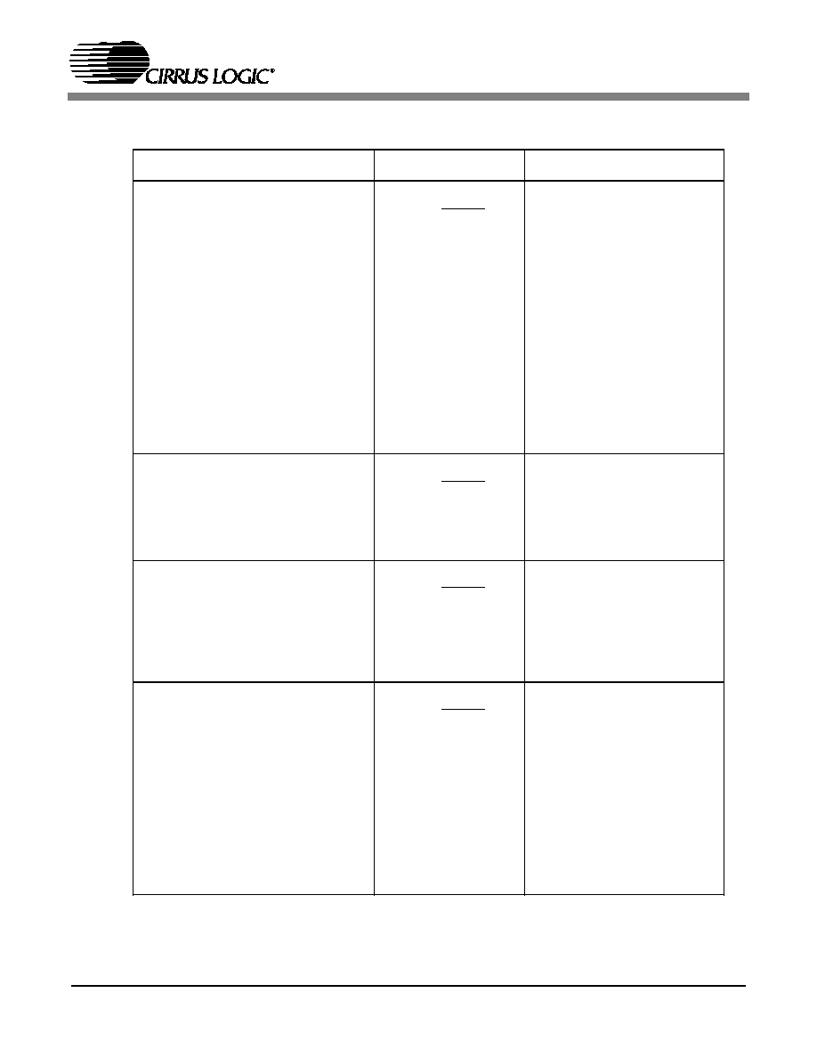
CS5376A
46
Filter Type
System Function
Filter Coefficients
SINC3 (Stage 1)
SINC3 (Stage 2)
SINC3 (Stage 3)
4
th
order decimate by 5
17 coefficients
4
1
5
1
1
)
(
-
-
=
-
-
z
z
z
H
h
0
= 1
h
1
= 4
h
2
= 10
h
3
= 20
h
4
= 35
h
5
= 52
h
6
= 68
h
7
= 80
h
8
= 85
h
9
= 80
h
10
= 68
h
11
= 52
h
12
= 35
h
13
= 20
h
14
= 10
h
15
= 4
h
16
= 1
SINC3 (Stage 4)
5
th
order decimate by 2
6 coefficients
5
1
2
1
1
)
(
-
-
=
-
-
z
z
z
H
h
0
= 1
h
1
= 5
h
2
= 10
h
3
= 10
h
4
= 5
h
5
= 1
SINC3 (Stage 5)
6
th
order decimate by 2
7 coefficients
6
1
2
1
1
)
(
-
-
=
-
-
z
z
z
H
h
0
= 1
h
1
= 6
h
2
= 15
h
3
= 20
h
4
= 15
h
5
= 6
h
6
= 1
SINC3 (Stage 6)
6
th
order decimate by 3
13 coefficients
6
1
3
1
1
)
(
-
-
=
-
-
z
z
z
H
h
0
= 1
h
1
= 6
h
2
= 21
h
3
= 50
h
4
= 90
h
5
= 126
h
6
= 141
h
7
= 126
h
8
= 90
h
9
= 50
h
10
= 21
h
11
= 6
h
12
= 1
Table 11. SINC3 Filter Coefficients
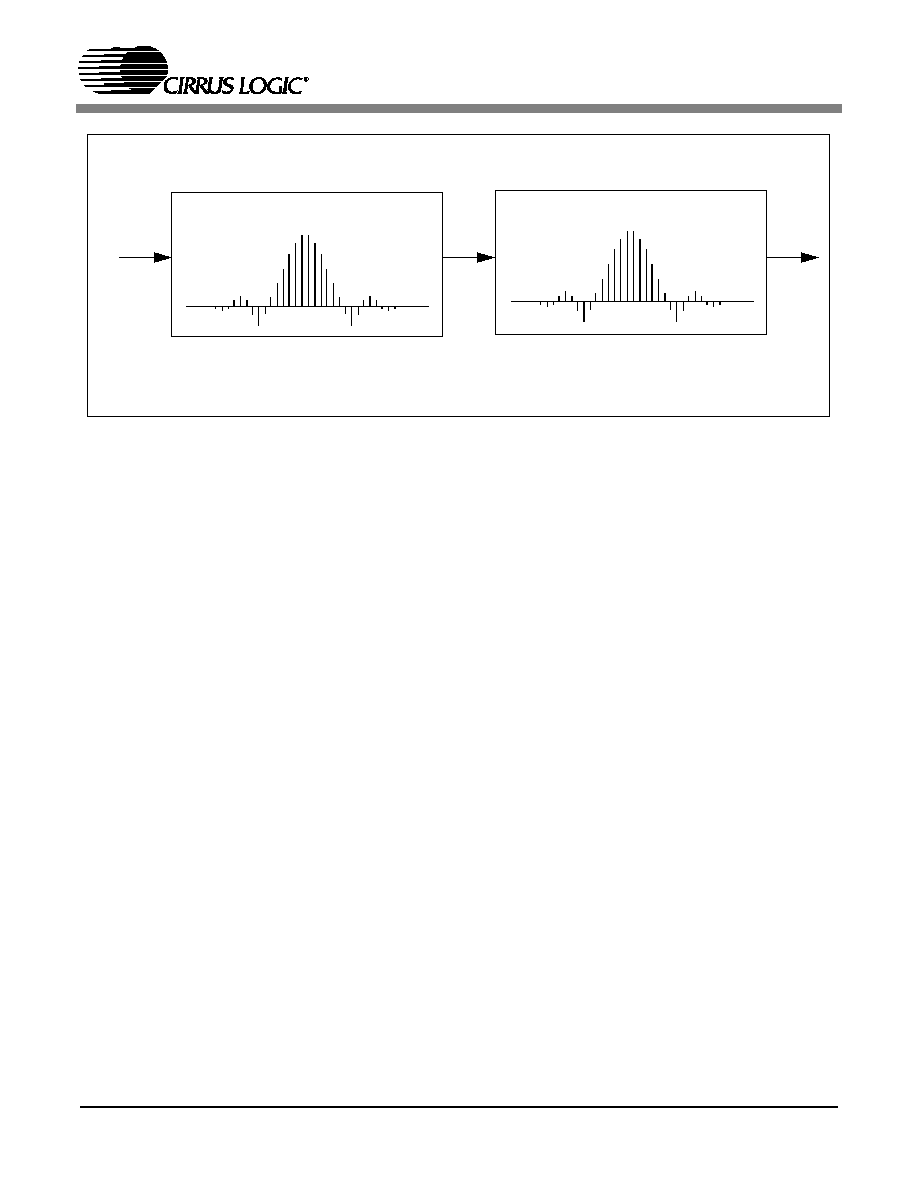
CS5376A
47
13. FIR FILTER
The finite impulse response (FIR) filter block con-
sists of two cascaded stages, FIR1 and FIR2. It
compensates for SINC filter droop and creates a
low-pass corner to block aliased components of the
input signal.
On-chip linear phase or minimum phase coeffi-
cients can be selected using a configuration com-
mand, or the coefficients can be programmed for a
custom filter response.
13.1 FIR1 Filter
The FIR1 filter stage has a decimate by four archi-
tecture. It compensates for SINC filter droop and
flattens the magnitude response of the pass band.
The on-chip linear and minimum phase coefficient
sets are 48-tap, with a maximum 255 programma-
ble coefficients. All coefficients are normalized to
24-bit two's complement full scale, 0x7FFFFF.
The characteristic equation for FIR1 is a convolu-
tion of the input values, X(n), and the filter coeffi-
cients, h(k), to produce an output value, Y.
Y = [h(k)*X(n-k)] + [h(k+1)*X(n-(k+1))] + ...
13.2 FIR2 Filter
The FIR2 filter stage has a decimate by two archi-
tecture. It creates a low-pass brick wall filter to
block aliased components of the input signal.
The on-chip linear and minimum phase coefficient
sets are 126-tap, with a maximum 255 programma-
ble coefficients. All coefficients are normalized to
24-bit two's complement full scale, 0x7FFFFF.
The characteristic equation for FIR2 is a convolu-
tion of the input values, X(n), and the filter coeffi-
cients, h(k), to produce an output value, Y.
Y = [h(k)*X(n-k)] + [h(k+1)*X(n-(k+1))] + ...
13.3 On-Chip FIR Coefficients
Two sets of on-chip linear phase and minimum
phase coefficients are available for FIR1 and FIR2.
Performance of the on-chip coefficient sets is very
good, with excellent ripple and stop band charac-
teristics as described in Figure 26 and Table 12.
Which on-chip coefficient set to use is selected by
a data word following the `Write ROM Coeffi-
cients' configuration command. See "Filter Coeffi-
cient Selection" on page 41 for information about
selecting on-chip coefficient sets.
FIR1 Filter - decimate by 4
FIR2 Filter - decimate by 2
Figure 25. FIR Filter Block Diagram

CS5376A
48
13.4 Programmable FIR Coefficients
A maximum of 255 + 255 coefficients can be pro-
grammed into FIR1 and FIR2 to create a custom
filter response. The total number of coefficients for
the FIR filter is fundamentally limited by the avail-
able computation cycles in the digital filter, which
itself is determined by the digital filter clock rate.
Custom filter sets should normalize the maximum
coefficient value to 24-bit two's complement full
scale, 0x7FFFFF, and scale all other coefficients
accordingly. To maintain maximum internal dy-
namic range, the CS5376A FIR filter performs
double precision calculations with an automatic
gain correction to scale the final output.
Custom FIR coefficients are uploaded using the
`Write FIR Coefficients' configuration command.
See "EEPROM Configuration Commands" on
page 28 or "Microcontroller Configuration Com-
mands" on page 35 for information about writing
custom FIR coefficients.
13.5 FIR Filter Synchronization
The FIR1 and FIR2 filters are synchronized to the
external system by the MSYNC signal, which is
generated from the SYNC input. The MSYNC sig-
nal sets a reference time (time 0) for all filter oper-
ations, and the FIR filters are restarted to phase
align with this reference time.
CS5376A
49
FIR1 � Single stage, fixed decimate by 4
Coefficient set 0: linear phase decimate by 4, 48 coefficients
Coefficient set 1: minimum phase decimate by 4, 48 coefficients
SINC droop compensation filter
FIR2 � Single stage, fixed decimate by 2
Coefficient set 0: linear phase decimate by 2, 126 coefficients
Coefficient set 1: minimum phase decimate by 2, 126 coefficients
Brick wall low-pass filter, flat to 40% f
s
Combined SINC + FIR digital filter specifications
Passband ripple less than +/- 0.01 dB below 40% f
s
Transition band -3 dB frequency at 42.89% f
s
Stopband attenuation greater than 130 dB above 50% f
s
Figure 26. FIR Filter Stages
SINC + FIR filters
FIR2
Output
Word
Rate
SINC
Deci-
mation
FIR1
Deci-
mation
FIR2
Deci-
mation
Total
Deci-
mation
Passband
Ripple
(
� dB)
Stopband
Atten-
uation
(dB)
4000 16
4
2 128
0.0042
130.38
2000 32
4
2 256
0.0045
130.38
1000 64
4
2 512
0.0040
130.42
500 128 4
2 1024
0.0041
130.42
333 192 4
2 1536
0.0080
130.45
250 256 4
2 2048
0.0064
130.43
200 320 4
2 2560
0.0041
130.43
125 512 4
2 4096
0.0046
130.42
100 640 4
2 5120
0.0040
130.43
50 1280 4
2 10240
0.0040
130.43
40 1600 4
2 12800
0.0036
130.43
25 2560 4
2 20480
0.0040
132.98
20 3200 4
2 25600
0.0036
130.43
10 6400 4
2 51200
0.0036
130.43
5 12800 4
2 102400
0.0036
130.43
1 64000 4
2 512000
0.0029
134.31
Table 12. FIR Filter Characteristics

CS5376A
50
Individual filter stage group delay (no IIR)
Decimation
Ratios
Number of
Coefficients
Group Delay
(Filter Stage
Input Rate)
SINC1
8 36
17.5
SINC2
Stage 4
2
7
3.0
Stages 3,4
2,2
6,7
8.5
Stages 2,3,4
2,2,2
5,6,7
19.0
Stages 1,2,3,4
2,2,2,2
5,5,6,7
40.0
SINC3
Stage 6
3
13
6.0
Stage 5
2
7
3.0
Stages 4,5
2,2
6,7
8.5
Stages 3,4,5
5,2,2
17,6,7
50.5
Stages 2,3,4,5
5,5,2,2
17,17,6,7
260.5
Stages 1,2,3,4,5
5,5,5,2,2
17,17,17,6,7
1310.5
FIR1
Coefficient Set 0
4
48
23.5
Coefficient Set 1
4
48
See Figure
FIR2
Coefficient Set 0
2
126
62.5
Coefficient Set 1
2
126
See Figure
Cumulative linear phase group delay (no IIR)
FIR2
Output
Word
Rate
SINC Output
Group Delay
(SINC Filter
Input Rate)
FIR1 Output
Group Delay
(SINC Filter
Input Rate)
FIR2 Output
Group Delay
(SINC Filter
Input Rate)
FIR2 Output
Group Delay
(FIR2 Output
Word Rate)
4000 41.5
417.5
4417.5
34.5117
2000 85.5
837.5
8837.5
34.5215
1000 169.5
1673.5
17673.5
34.5186
500 337.5
3345.5
35345.5 34.5171
333 553.5
5065.5
53065.5 34.5479
250 721.5
6737.5
70737.5 34.5398
200 849.5
8369.5
88369.5 34.5193
125 1425.5
13457.5 141457.5 34.5355
100 1701.5
16741.5 176741.5 34.5198
50 3401.5
33481.5 353481.5 34.5197
40 4209.5
41809.5 441809.5 34.5164
25 6801.5
66961.5 706961.5 34.5196
20 8421.5
83621.5 883621.5 34.5165
10 16841.5 167241.5 1767241.5 34.5164
5 33681.5 334481.5 3534481.5 34.5164
1 168081.5 1672081.5
17672081.5 34.5158
Table 13. SINC + FIR Group Delay

CS5376A
51
Minimum phase group delay
FIR1
Minimum
Phase Group
Delay
(Normalized
frequency)
FIR2
Minimum
Phase Group
Delay
(Normalized
frequency)
Table 14. Minimum Phase Group Delay

CS5376A
52
Filter Type
Filter Coefficients
(normalized 24-bit)
FIR1 (Coefficient set 0)
Low pass, SINC compensation
Linear phase decimate by 4
48 coefficients
h
0
= 558 h
24
= 8388607
h
1
= 1905 h
25
= 7042723
h
2
= 3834 h
26
= 4768946
h
3
= 5118 h
27
= 2266428
h
4
= 365 h
28
= 189436
h
5
= -14518 h
29
= -1053303
h
6
= -39787 h
30
= -1392827
h
7
= -67365 h
31
= -1084130
h
8
= -69909 h
32
= -496361
h
9
= -19450 h
33
= 39864
h
10
= 97434 h
34
= 332367
h
11
= 258881 h
35
= 375562
h
12
= 375562 h
36
= 258881
h
13
= 332367 h
37
= 97434
h
14
= 39864 h
38
= -19450
h
15
= -496361 h
39
= -69909
h
16
= -1084130 h
40
= -67365
h
17
= -1392827 h
41
= -39787
h
18
= -1053303 h
42
= -14518
h
19
= 189436 h
43
= 365
h
20
= 2266428 h
44
= 5118
h
21
= 4768946 h
45
= 3834
h
22
= 7042723 h
46
= 1905
h
23
= 8388607 h
47
= 558
FIR1 (Coefficient set 1)
Low pass, SINC compensation
Minimum phase decimate by 4
48 coefficients
h
0
= 3337 h
24
= 555919
h
1
= 22258 h
25
= -165441
h
2
= 88284 h
26
= -581479
h
3
= 266742 h
27
= -617500
h
4
= 655747 h
28
= -388985
h
5
= 1371455 h
29
= -99112
h
6
= 2502684 h
30
= 114761
h
7
= 4031988 h
31
= 186557
h
8
= 5783129 h
32
= 141374
h
9
= 7396359 h
33
= 58582
h
10
= 8388607 h
34
= -12664
h
11
= 8325707 h
35
= -42821
h
12
= 6988887 h
36
= -35055
h
13
= 4531706 h
37
= -16792
h
14
= 1507479 h
38
= 367
h
15
= -1319126 h
39
= 7929
h
16
= -3207750 h
40
= 5926
h
17
= -3736028 h
41
= 2892
h
18
= -2980701 h
42
= 23
h
19
= -1421498 h
43
= -1164
h
20
= 237307 h
44
= -538
h
21
= 1373654 h
45
= -238
h
22
= 1711919 h
46
= 18
h
23
= 1322371 h
47
= 113
Figure 27. FIR1 Coefficients

CS5376A
53
Filter Type
Filter Coefficients
(normalized 24-bit)
FIR2 (Coefficient set 0)
Low pass, passband to 40% f
s
Linear phase decimate by 2
126 coefficients
h
0
= -71 h
63
= 8388607
h
1
= -371 h
64
= 3875315
h
2
= -870 h
65
= -766230
h
3
= -986 h
66
= -1854336
h
4
= 34 h
67
= -137179
h
5
= 1786 h
68
= 1113788
h
6
= 2291 h
69
= 454990
h
7
= 291 h
70
= -642475
h
8
= -2036 h
71
= -553873
h
9
= -943 h
72
= 298975
h
10
= 2985 h
73
= 533334
h
11
= 3784 h
74
= -49958
h
12
= -1458 h
75
= -443272
h
13
= -5808 h
76
= -116005
h
14
= -1007 h
77
= 318763
h
15
= 7756 h
78
= 208018
h
16
= 5935 h
79
= -187141
h
17
= -7135 h
80
= -238025
h
18
= -11691 h
81
= 68863
h
19
= 3531 h
82
= 221211
h
20
= 17500 h
83
= 22850
h
21
= 4388 h
84
= -174452
h
22
= -20661 h
85
= -81993
h
23
= -15960 h
86
= 114154
h
24
= 18930 h
87
= 109009
h
25
= 29808 h
88
= -54172
h
26
= -9795 h
89
= -109189
h
27
= -42573 h
90
= 4436
h
28
= -7745 h
91
= 90744
h
29
= 49994 h
92
= 29702
h
30
= 33021 h
93
= -62651
h
31
= -47092 h
94
= -47092
h
32
= -62651 h
95
= 33021
h
33
= 29702 h
96
= 49994
h
34
= 90744 h
97
= -7745
h
35
= 4436 h
98
= -42573
h
36
= -109189 h
99
= -9795
h
37
= -54172 h
100
= 29808
h
38
= 109009 h
101
= 18930
h
39
= 114154 h
102
= -15960
h
40
= -81993 h
103
= -20661
h
41
= -174452 h
104
= 4388
h
42
= 22850 h
105
= 17500
h
43
= 221211 h
106
= 3531
h
44
= 68863 h
107
= -11691
h
45
= -238025 h
108
= -7135
h
46
= -187141 h
109
= 5935
h
47
= 208018 h
110
= 7756
h
48
= 318763 h
111
= -1007
h
49
= -116005 h
112
= -5808
h
50
= -443272 h
113
= -1458
h
51
= -49958 h
114
= 3784
h
52
= 533334 h
115
= 2985
h
53
= 298975 h
116
= -943
h
54
= -553873 h
117
= -2036
h
55
= -642475 h
118
= 291
h
56
= 454990 h
119
= 2291
h
57
= 1113788 h
120
= 1786
h
58
= -137179 h
121
= 34
h
59
= -1854336 h
122
= -986
h
60
= -766230 h
123
= -870
h
61
= 3875315 h
124
= -371
h
62
= 8388607 h
125
= -71
Figure 28. FIR2 Linear Phase Coefficients

CS5376A
54
Filter Type
Filter Coefficients
(normalized 24-bit)
FIR2 (Coefficient set 1)
Low pass, passband to 40% f
s
Minimum phase decimate by 2
126 coefficients
h
0
= 4019 h
63
= 67863
h
1
= 43275 h
64
= -190800
h
2
= 235427 h
65
= -128546
h
3
= 848528 h
66
= 114197
h
4
= 2240207 h
67
= 147750
h
5
= 4525758 h
68
= -46352
h
6
= 7077833 h
69
= -143269
h
7
= 8388607 h
70
= -13290
h
8
= 6885673 h
71
= 114721
h
9
= 2483461 h
72
= 51933
h
10
= -2538963 h
73
= -75952
h
11
= -4800543 h
74
= -68746
h
12
= -2761696 h
75
= 38171
h
13
= 1426109 h
76
= 68492
h
14
= 3624338 h
77
= -7856
h
15
= 1820814 h
78
= -57526
h
16
= -1695825 h
79
= -12540
h
17
= -2885148 h
80
= 41717
h
18
= -605252 h
81
= 23334
h
19
= 2135021 h
82
= -25516
h
20
= 1974197 h
83
= -26409
h
21
= -630111 h
84
= 11717
h
22
= -2168177 h
85
= 24246
h
23
= -750147 h
86
= -1620
h
24
= 1516192 h
87
= -19248
h
25
= 1550127 h
88
= -4610
h
26
= -508445 h
89
= 13356
h
27
= -1686937 h
90
= 7526
h
28
= -437822 h
91
= -7887
h
29
= 1308705 h
92
= -8016
h
30
= 1069556 h
93
= 3559
h
31
= -657282 h
94
= 7023
h
32
= -1301014 h
95
= -598
h
33
= -30654 h
96
= -5350
h
34
= 1173754 h
97
= -1097
h
35
= 579643 h
98
= 3579
h
36
= -803111 h
99
= 1806
h
37
= -895851 h
100
= -2058
h
38
= 328399 h
101
= -1859
h
39
= 962522 h
102
= 936
h
40
= 124678 h
103
= 1558
h
41
= -820948 h
104
= -224
h
42
= -466657 h
105
= -1129
h
43
= 545674 h
106
= -152
h
44
= 652827 h
107
= 718
h
45
= -220448 h
108
= 290
h
46
= -680495 h
109
= -395
h
47
= -80886 h
110
= -290
h
48
= 578844 h
111
= 178
h
49
= 306445 h
112
= 227
h
50
= -395302 h
113
= -53
h
51
= -431004 h
114
= -151
h
52
= 181900 h
115
= -5
h
53
= 454403 h
116
= 86
h
54
= 15856 h
117
= 23
h
55
= -395525 h
118
= -42
h
56
= -166123 h
119
= -22
h
57
= 284099 h
120
= 17
h
58
= 253485 h
121
= 14
h
59
= -152407 h
122
= -5
h
60
= -277888 h
123
= -7
h
61
= 28526 h
124
= 1
h
62
= 250843 h
125
= 3
Figure 29. FIR2 Minimum Phase Coefficients

CS5376A
55
14. IIR FILTER
The infinite impulse response (IIR) filter block
consists of two cascaded stages, IIR1 and IIR2. It
creates a high-pass corner to block very low-fre-
quency and DC components of the input signal.
On-chip IIR1 and IIR2 coefficients can be selected
using a configuration command, or the coefficients
can be programmed for a custom filter response.
14.1 IIR Architecture
The architecture of the IIR filter is automatically
determined when the output filter stage is selected
in the FILTCFG register. Selecting the 1st order
IIR1 filter bypasses the 2nd order stage, while se-
lecting the 2nd order IIR2 filter bypasses the 1st or-
der stage. Selection of the 3rd order IIR3 filter
enables both the 1st and 2nd order stages.
14.2 IIR1 Filter
The 1st order IIR filter stage is a direct form filter
with three coefficients: a11, b10, and b11. Coeffi-
cients of a 1st order IIR are inherently normalized
to one, and should be scaled to 24-bit two's com-
plement full scale, 0x7FFFFF.
The characteristic equations for the 1st order IIR
include an input value, X, an output value, Y, and
two intermediate values, W1 and W2, separated by
a delay element (z
-1
).
W2 = W1
W1 = X + (-a11 * W2)
Y = (W1 * b10) + (W2 * b11)
14.3 IIR2 Filter
The 2nd order IIR filter stage is a direct form filter
with five coefficients: a21, a22, b20, b21, and b22.
Coefficients of a 2nd order IIR are inherently nor-
malized to two, and should be scaled to 24-bit
two's complement full scale, 0x7FFFFF. Normal-
ization effectively divides the 2nd order coeffi-
cients in half relative to the input, and requires
modification of the characteristic equations.
The characteristic equations for the 2nd order IIR
include an input value, X, an output value, Y, and
three intermediate values, W3, W4, and W5, each
separated by a delay element (z
-1
). The following
Z
-1
Z
-1
Z
-1
-a
11
b
11
b
10
-a
21
-a
22
b
21
b
22
b
20
Figure 30. IIR Filter Block Diagram
1st Order IIR1
2nd Order IIR2
3rd Order IIR3 implemented by
running both IIR1 and IIR2 stages

CS5376A
56
characteristic equations model the operation of the
2nd order IIR filter with unnormalized coefficients.
W5 = W4
W4 = W3
W3 = X + (-a21 * W4) + (-a22 * W5)
Y = (W3 * b20) + (W4 * b21) + (W5 * b22)
Internally, the CS5376A uses normalized coeffi-
cients to perform the 2nd order IIR filter calcula-
tion, which changes the algorithm slightly. The
following characteristic equations model the oper-
ation of the 2nd order IIR filter when using normal-
ized coefficients.
W5 = W4
W4 = W3
W3 = 2 * [(X / 2) + (-a21 * W4) + (-a22 * W5)]
Y = 2 * [(W3 * b20) + (W4 * b21) + (W5 * b22)]
14.4 IIR3 Filter
The 3rd order IIR filter is implemented by running
both the 1st order and 2nd order IIR filter stages. It
can be modeled by cascading the characteristic
equations of the 1st order and 2nd order IIR stages.
14.5 On-Chip IIR Coefficients
Five sets of on-chip coefficients are available for
IIR1 and IIR2, each providing a 3 Hz high-pass
Butterworth response at different output word
rates. Characteristics of the on-chip coefficient sets
are described in Figure 31 and Table 14.
Which on-chip coefficient set to use is selected by
a data word following the `Write ROM Coeffi-
cients' configuration command. See "Filter Coeffi-
cient Selection" on page 41 for information about
selecting on-chip coefficient sets.
14.6 Programmable IIR Coefficients
A maximum of 3 + 5 coefficients can be pro-
grammed into IIR1 and IIR2 to create a custom fil-
ter response. Custom filter sets should normalize
the coefficients to 24-bit two's complement full
scale, 0x7FFFFF. To maintain maximum internal
dynamic range, the CS5376A IIR filter performs
double precision calculations with an automatic
gain correction to scale the final output.
Custom IIR coefficients are uploaded using the
`Write IIR Coefficients' configuration command.
See "EEPROM Configuration Commands" on
page 28 or "Microcontroller Configuration Com-
mands" on page 35 for information about writing
custom IIR coefficients.
14.7 IIR Filter Synchronization
The IIR filter is not synchronized to the external
system directly, only indirectly through the syn-
chronization of the SINC and FIR filters. Because
IIR filters have `infinite' memory, a discontinuity
in the input data stream from a synchronization
event can require significant time to settle out. The
exact settling time depends on the size of the dis-
continuity and the filter coefficient characteristics.

CS5376A
57
IIR1 � Single stage, no decimation
1
st
order no decimation, 3 coefficients
Coefficient set 0: high-pass, corner 0.15% f
s
(3 Hz at 2000 SPS)
Coefficient set 1: high-pass, corner 0.30% f
s
(3 Hz at 1000 SPS)
Coefficient set 2: high-pass, corner 0.60% f
s
(3 Hz at 500 SPS)
Coefficient set 3: high-pass, corner 0.90% f
s
(3 Hz at 333 SPS)
Coefficient set 4: high-pass, corner 1.20% f
s
(3 Hz at 250 SPS)
IIR2 � Single stage, no decimation
2
nd
order no decimation, 5 coefficients
Coefficient set 0: high-pass, corner 0.15% f
s
(3 Hz at 2000 SPS)
Coefficient set 1: high-pass, corner 0.30% f
s
(3 Hz at 1000 SPS)
Coefficient set 2: high-pass, corner 0.60% f
s
(3 Hz at 500 SPS)
Coefficient set 3: high-pass, corner 0.90% f
s
(3 Hz at 333 SPS)
Coefficient set 4: high-pass, corner 1.20% f
s
(3 Hz at 250 SPS)
IIR3 � Two stage, no decimation
3
rd
order no decimation, 8 coefficients
(Combined IIR1 and IIR2 filter responses)
Coefficient set 0,0: high-pass, corner 0.20% f
s
(4 Hz at 2000 SPS)
Coefficient set 1,1: high-pass, corner 0.41% f
s
(4 Hz at 1000 SPS)
Coefficient set 2,2: high-pass, corner 0.82% f
s
(4 Hz at 500 SPS)
Coefficient set 3,3: high-pass, corner 1.22% f
s
(4 Hz at 333 SPS)
Coefficient set 4,4: high-pass, corner 1.63% f
s
(4 Hz at 250 SPS)
Figure 31. IIR Filter Stages
IIR filters
IIR1 Coeff
Selection
IIR1
Corner
Frequency
IIR2 Coeff
Selection
IIR2
Corner
Frequency
IIR3 Coeff
Selection
IIR3
Corner
Frequency
0 0.15%
f
s
0 0.15%
f
s
0,0
0.2041%
f
s
1 0.30%
f
s
1 0.30%
f
s
1,1
0.4074%
f
s
2 0.60%
f
s
2 0.60%
f
s
2,2
0.8152%
f
s
3 0.90%
f
s
3 0.90%
f
s
3,3
1.2222%
f
s
4 1.20%
f
s
4 1.20%
f
s
4,4
1.6293%
f
s
Table 14. IIR Filter Characteristics

CS5376A
58
Filter Type
System Function
Filter Coefficients
(normalized 24-bit)
IIR1 (Coefficient set 0)
1
st
order, high pass
Corner at 0.15% f
s
3 coefficients
+
+
=
-
-
1
11
1
11
10
1
)
(
z
a
z
b
b
z
H
a
11
= -8309916
b
10
= 8349262
b
11
= -8349262
IIR1 (Coefficient set 1)
1
st
order, high pass
Corner at 0.30% f
s
3 coefficients
+
+
=
-
-
1
11
1
11
10
1
)
(
z
a
z
b
b
z
H
a
11
= -8231957
b
10
= 8310282
b
11
= -8310282
IIR1 (Coefficient set 2)
1
st
order, high pass
Corner at 0.60% f
s
3 coefficients
+
+
=
-
-
1
11
1
11
10
1
)
(
z
a
z
b
b
z
H
a
11
= -8078179
b
10
= 8233393
b
11
= -8233393
IIR1 (Coefficient set 3)
1
st
order, high pass
Corner at 0.90% f
s
3 coefficients
+
+
=
-
-
1
11
1
11
10
1
)
(
z
a
z
b
b
z
H
a
11
= -7927166
b
10
= 8157887
b
11
= -8157887
IIR1 (Coefficient set 4)
1
st
order, high pass
Corner at 1.20% f
s
3 coefficients
+
+
=
-
-
1
11
1
11
10
1
)
(
z
a
z
b
b
z
H
a
11
= -7778820
b
10
= 8083714
b
11
= -8083714
Filter Type
System Function
Filter Coefficients
(normalized 24-bit)
IIR2 (Coefficient set 0)
2
nd
order, high pass
Corner at 0.15% f
s
5 coefficients
+
+
+
+
=
-
-
-
-
1
22
1
21
1
22
1
21
20
1
)
(
z
a
z
a
z
b
z
b
b
z
H
a
21
= -8332704
a
22
= 4138771
b
20
= 4166445
b
21
= -8332890
b
22
= 4166445
IIR2 (Coefficient set 1)
2
nd
order, high pass
Corner at 0.30% f
s
5 coefficients
+
+
+
+
=
-
-
-
-
1
22
1
21
1
22
1
21
20
1
)
(
z
a
z
a
z
b
z
b
b
z
H
a
21
= -8276806
a
22
= 4083972
b
20
= 4138770
b
21
= -8277540
b
22
= 4138770
IIR2 (Coefficient set 2)
2
nd
order, high pass
Corner at 0.60% f
s
5 coefficients
+
+
+
+
=
-
-
-
-
1
22
1
21
1
22
1
21
20
1
)
(
z
a
z
a
z
b
z
b
b
z
H
a
21
= -8165041
a
22
= 3976543
b
20
= 4083972
b
21
= -8167944
b
22
= 4083972
IIR2 (Coefficient set 3)
2
nd
Order, high pass
Corner at 0.90% f
s
5 coefficients
+
+
+
+
=
-
-
-
-
1
22
1
21
1
22
1
21
20
1
)
(
z
a
z
a
z
b
z
b
b
z
H
a
21
= -8053350
a
22
= 3871939
b
20
= 4029898
b
21
= -8059796
b
22
= 4029898
IIR2 (Coefficient set 4)
2
nd
order, high pass
Corner at 1.20% f
s
5 coefficients
+
+
+
+
=
-
-
-
-
1
22
1
21
1
22
1
21
20
1
)
(
z
a
z
a
z
b
z
b
b
z
H
a
21
= -7941764
a
22
= 3770088
b
20
= 3976539
b
21
= -7953078
b
22
= 3976539
Table 15. IIR Filter Coefficients

CS5376A
59
15. GAIN AND OFFSET CORRECTION
The CS5376A digital filter can apply independent
gain and offset corrections to the data of each mea-
surement channel. Also, an offset calibration algo-
rithm can automatically calculate offset correction
values for each channel.
Gain correction values are written to the GAINx
registers (0x21-0x24), while offset correction val-
ues are written to the OFFSETx registers (0x25-
0x28). Gain and offset corrections are enabled by
the USEGR and USEOR bits in the FILTCFG reg-
ister (0x20).
When enabled, the offset calibration algorithm will
automatically calculate offset correction values for
each channel and write them into the OFFSETx
registers. Offset calibration is enabled by writing
the EXP and ORCAL bits in FILTCFG.
15.1 Gain Correction
Gain correction in the CS5376A normalizes sensor
gains in multi-sensor networks. It requires exter-
nally calculated correction values to be written into
the GAINx registers (0x21-0x24).
Gain correction values are 24-bit two's comple-
ment with unity gain defined as full scale,
0x7FFFFF. Gain correction always scales to a frac-
tional value, and can never gain the digital filter
data greater than one.
Output Value = Data * (GAIN / 0x7FFFFF)
Unity Gain: GAIN = 0x7FFFFF
50% Gain: GAIN = 0x3FFFFF
Zero Gain: GAIN = 0x000000
Once the GAIN registers are written, the USEGR
bit in the FILTCFG register enables gain correc-
tion.
15.2 Offset Correction
Offset correction in the CS5376A cancels the DC
bias of a measurement channel by subtracting the
Figure 32. Gain and Offset Correction
FIR
IIR
Filters
Filter
Output to High Speed Serial Data Port (SD Port)
Offset
Correction
Output Rate 4000 SPS ~ 1 SPS
SINC
Filter
MDI Input
512 kHz
Correction
Gain
Offset
Calibration
4
4
4
4

CS5376A
60
value in the OFFSETx registers (0x25-0x28) from
the digital filter output data word.
Offset correction values are 24-bit two's comple-
ment with a maximum positive value of 0x7FFFFF,
and a maximum negative value of 0x800000. If ap-
plying an offset correction causes the final result to
exceed a 24-bit two's complement maximum, the
output data will saturate to that maximum value.
Output Data = Input Data - Offset Correction
Max Positive Output Value = 0x7FFFFF
Max Negative Output Value = 0x800000
Once the OFFSET registers are written, the USE-
OR bit in the FILTCFG register enables offset cor-
rection.
15.3 Offset Calibration
An offset calibration algorithm in the CS5376A
can automatically calculate offset correction val-
ues. When using the offset calibration algorithm,
background noise data should be used as the basis
for calculating the offset value of each measure-
ment channel.
The offset calibration algorithm is an exponential
averaging function that places increased weight on
more recent digital filter data. The exponential
weighting factor is set by the EXP bits in the
FILTCFG register, with larger exponent values
producing a smoother averaging function that re-
quires a longer settling time, and smaller values
producing a noisier averaging function that re-
quires a shorter settling time. Typical exponential
values range from 0x05 to 0x0F, depending on the
available settling time.
The characteristic equations of the offset calibra-
tion algorithm include an input value, X, an output
value, Y, a summation value, YSUM, a sample in-
dex, n, and an exponential value, EXP.
Y(n) = X(n) - [YSUM(n-1) >> EXP]
YSUM(n) = Y(n) + YSUM(n-1)
Offset Correction = YSUM >> EXP
Once the EXP bits are written, the ORCAL bit in
the FILTCFG register is set to enable offset calibra-
tion. When enabled, updated offset correction val-
ues are automatically written to the OFFSETx
registers. When the offset calibration algorithm is
fully settled, the ORCAL bit is cleared to maintain
the final values in the OFFSETx registers.

CS5376A
61
16. SERIAL DATA PORT
Once digital filtering is complete, each 24-bit out-
put sample is combined with an 8-bit status byte.
These 32-bit data words are written to an 8-deep
FIFO buffer and then transmitted to the communi-
cations channel through a high speed serial data
port (SD port).
16.1 Pin Descriptions
SDTKI - Pin 64
Token input, requests an SD port transaction.
SDRDY - Pin 61
Data ready output signal, active low. Open drain
output requiring a 10 k
pull-up resistor.
SDCLK - Pin 62
Serial clock input.
SDDAT - Pin 60
Serial data output. Data valid on rising edge of
SDCLK, transition on falling edge.
SDTKO - Pin 63
Token output, ends an SD port transaction. Passes
through the SDTKI signal when no data is available
in the SD port output FIFO.
16.2 SD Port Data Format
Serial data transactions transfer 32-bit words. Each
word consists of an 8-bit status byte followed by a
24-bit output sample. The status byte, shown in
Figure 34, has an MFLAG bit, channel bits, a time
break bit, and a FIFO overflow bit.
MFLAG Bit - MFLAG
The MFLAG bit is set when an MFLAG signal is
received on the MFLAG1-MFLAG4 pins. When
received, that channel MFLAG bit is set in the next
output word. See "Modulator Interface" on page 39
for more information about MFLAG.
Channel Bits - CH[1:0]
Channel bits indicate from which conversion chan-
nel the data word is from. The channel number,
CH[1:0], is zero based.
CH[1:0] = 00 = Channel 1
CH[1:0] = 01 = Channel 2
CH[1:0] = 10 = Channel 3
CH[1:0] = 11 = Channel 4
Time Break Bit - TB
The time break bit marks a timing reference based
on a rising edge into the TIMEB pin. After a pro-
grammed delay, the TB bit in the status byte is set
CS5376A
SDTKI
SDTKO
Figure 33. Serial Data Port Block Diagram
System Telemetry
SDDAT
SDRDY
SDCLK
Token Out
Token In
Data Ready
Data In
Clock Out

CS5376A
62
for one output sample in all channels. The TIME-
BRK digital filter register (0x29) programs the
sample delay for the TB bit output. See "Time
Break Controller" on page 68 for more information
about time break.
FIFO Overflow Bit - W
The FIFO overflow bit indicates an error condition
in the SD port data FIFO, and is set if new digital
filter data overwrites a FIFO location containing
data which has not yet been sent.
The W bit is sticky, meaning it persists indefinitely
once set. Clearing the W bit requires sending the
`Filter Stop' and `Filter Start' configuration com-
mands to reinitialize the data FIFO.
Conversion Data Word
The lower 24-bits of the SD port output data word
is the conversion sample for the specified channel.
Conversion data is 24-bit two's complement for-
mat.
16.3 SD Port Transactions
The SD port can operate in two modes depending
how the SDTKI pin is connected: request mode
where data is output when requested by the com-
munications channel, or continuous mode where
data is output immediately when ready.
16.3.1 Request Mode
To initiate SD port transactions on request, SDTKI
is connected to an active high polling signal from
the communications channel. A rising edge into
SDTKI when new data is available in the SD port
FIFO causes the CS5376A to initiate an SD port
transaction by driving SDRDY low. If data is not
yet available in the SD port FIFO, the SDTKI sig-
nal is passed through to the SDTKO output.
Once an SD port transaction is initiated, serial
clocks into SDCLK cause data to be output to
SDDAT, as shown in Figure 35. When all available
Data
Status
0
23
31
--
MFLAG
CH[1]
CH[0]
W
31
29
30
28
27
26
25
24
Figure 34. SD Port Data Format
TB
--
Word 1
Word 4
Word 2
Word 3
Status
Data
128 bits
--
00 - Channel 1
01 - Channel 2
10 - Channel 3
11 - Channel 4
0 - Modulator Ok
1 - Modulator Error
0 - No Time Break
1 - Time Break
0 - FIFO Ok
1 - FIFO Overflow

CS5376A
63
data is read from the SD port data FIFO, SDRDY is
released and SDTKO is pulsed high for 100 nS.
16.3.2 Continuous Mode
To have the CS5376A automatically initiate SD
port transactions whenever data becomes available,
connect SDTKI to a 4 MHz or slower clock source
such as MCLK/2. The first rising edge into SDTKI
after data becomes available in the SD port FIFO
causes the CS5376A to initiate an SD port transac-
tion by driving SDRDY low. If data is not available
in the SD port FIFO, the SDTKI signal is passed
through to the SDTKO output.
Once an SD port transaction is initiated, serial
clocks into SDCLK cause data to be output to
SDDAT, as shown in Figure 35. When all available
data is read from the SD port data FIFO, SDRDY is
released and SDTKO is pulsed high for 100 nS.
SDRDY
SDCLK
SDDAT
Figure 35. SD Port Transaction
MSB
LSB
SDTKI
SDTKO

CS5376A
64
17. TEST BIT STREAM GENERATOR
The CS5376A test bit stream (TBS) generator cre-
ates sine wave or impulse
bit stream data to
drive an external test DAC. The TBS digital output
can also be internally connected to the MDATA in-
puts for loopback testing of the digital filter.
17.1 Pin Descriptions
TBSDATA - Pin 9
Test bit stream 1-bit
data output.
TBSCLK - Pin 8
Test bit stream clock output. Not used by the
CS4373 test DAC.
17.2 TBS Architecture
The test bit stream generator consists of a data in-
terpolator and a digital
modulator. It receives
periodic 24-bit data from the digital filter to create
a 1-bit
data output on the TBSDATA pin. It also
creates a clock signal at the data rate, output to the
TBSCLK pin.
The TBS input data from the digital filter is scaled
by the TBSGAIN register (0x2B). Maximum stable
amplitude is 0x04FFFF, with 0x04B000 approxi-
mately full scale for the CS4373 test DAC. The full
scale 1-bit
output from the TBS generator is de-
fined as 25% minimum and 75% maximum one's
density.
17.3 TBS Configuration
Configuration options for the TBS generator are set
through the TBSCFG register (0x2A). Gain scaling
of the TBS generator output is set by the TBSGAIN
register (0x2B).
Interpolation Factor - INTP[7:0]
Selects how many times the interpolator uses a data
point when generating the output bit stream. Inter-
polation is zero based and represents one greater
than the programmed register value.
Operational Mode - TMODE
Selects between sine wave or impulse output mode.
Clock Rate - RATE[2:0]
Selects the TBSDATA and TBSCLK output rate.
Synchronization - TSYNC
Enables synchronization of the TBS output phase
to the MSYNC signal.
Digital
Modulator
24-bit
1-bit
TBSDATA
Digital Filter
TBSGAIN Register
24-bit
Figure 36. Test Bit Stream Generator Block Diagram
Data Bus
TBSCLK
Clock Generation
TBSCFG Register
CS5376A
65
Clock Delay - CDLY[2:0]
Programs a fractional delay for TBSCLK with a 1/8
clock period resolution.
Loopback - LOOP
Enables digital loopback from the TBS output to
the MDATA inputs.
Run - RUN
Enables the test bit stream generator.
Data Delay - DDLY[5:0]
Programs full period delays for TBSDATA, up to a
maximum of 63 bits.
Gain - TBSGAIN[23:0]
Scales the amplitude of the sine wave output and
generated impulse. Maximum 0x04FFFF, nominal
0x04B000.
17.4 TBS Data Source
Data to create test signals is loaded into digital fil-
ter memory by configuration commands. The on-
chip sine wave data is suitable for most tests,
though custom data is required to support custom
signal frequencies. See "EEPROM Configuration
Commands" on page 28 or "Microcontroller Con-
figuration Commands" on page 35 for information
about programming TBS data.
TBS ROM Data
An on-chip 24-bit 1024 point digital sine wave is
stored on the CS5376A. When selected by the
`Write TBS ROM Data' configuration command,
the TBS generator can produce the test signal fre-
quencies listed in Table 16. Additional discrete test
frequencies and output rates can be programmed
with the on-chip data by varying the interpolation
factor and output rate.
Test Bit Stream Characteristic Equation:
(Signal Freq) * (# TBS Data) * (Interpolation + 1) = Output Rate
Example: (31.25 Hz) * (1024) * (0x07 + 1) = 256 kHz
Signal
Frequency
(TBSDATA)
Output
Rate
(TBSCLK)
Output Rate
Selection
(RATE)
Interpolation
Selection
(INTP)
10.00 Hz
256 kHz
0x4
0x18
10.00 Hz
512 kHz
0x5
0x31
25.00 Hz
256 kHz
0x4
0x09
25.00 Hz
512 kHz
0x5
0x13
31.25 Hz
256 kHz
0x4
0x07
31.25 Hz
512 kHz
0x5
0x0F
50.00 Hz
256 kHz
0x4
0x04
50.00 Hz
512 kHz
0x5
0x09
125.00 Hz
256 kHz
0x4
0x01
125.00 Hz
512 kHz
0x5
0x03
Table 16. TBS Configurations Using On-chip Data
CS5376A
66
Custom TBS Data
If a required test frequency cannot be generated us-
ing the on-chip test bit stream data, a custom data
set can be written into the CS5376A. The number
of data points to write, up to a maximum of 1024,
depends on the required test signal frequency, out-
put rate, and available interpolation factors. Cus-
tom data sets must be continuous on the ends; i.e.
when copied end-to-end the data set must produce
a smooth curve.
17.5 TBS Sine Wave Output
When the TMODE bit in the TBSCFG register is
low, the TBS generator operates in sine wave
mode. In this mode, sine wave data from digital fil-
ter memory is used to create a sine wave test signal
that can drive a test DAC. Sine wave frequency and
output data rate are calculated as shown by the
characteristic equation of Table 16.
The sine wave maximum
one's density output
from the TBS generator is set by the TBSGAIN
register. TBSGAIN can be programmed up to a
maximum of 0x04FFFF, with the TBS generator
unstable for higher amplitudes. For the CS4373 test
DAC, a gain value of 0x04B000 produces an ap-
proximately full scale sine wave output (5 V
pp
dif-
ferential).
17.6 TBS Impulse Output
If the TMODE bit in TBSCFG is set high, the TBS
generator operates in impulse mode. In this mode,
the value in TBSGAIN sets the amplitude of the
generated impulse. Impulse amplitude and period
are calculated as shown in Table 17.
To create an impulse from the TBS generator, the
TBSGAIN register should be set to maximum,
0x04FFFF, and the INTP bits in TBSCFG should
also be set to maximum, 0xFF. The RATE bits
should be set to produce data at the correct rate for
the selected test DAC.
A rising edge on the TIMEB pin triggers the im-
pulse output. When impulse mode is enabled but no
TIMEB input is received, the TBS generator uses a
negated TBSGAIN register as a repetitive input
value. When a rising edge is recognized on the
TIMEB pin, a single positive TBSGAIN value is
written to the TBS generator to create the impulse.
17.7 TBS Loopback Testing
Included as part of the CS5376A test bit stream
generator is a feedback path to the digital filter
MDATA inputs. This loopback mode provides a
fully digital signal path to test the TBS generator,
digital filter, and data collection interface. Digital
Test Bit Stream Impulse Characteristics:
Interpolation
Selection
(INTP)
Output Rate
Selection
(RATE)
Pulse Width
from CS4373
Gain Scale
Factor
(TBSGAIN)
Pulse Height
from CS4373
0xFF
0x5
500
�s
0x04B000
860 mV
0xFF
0x4
1 ms
0x04B000
820 mV
0xFF
0x3
2 ms
0x04B000
820 mV
0x7F
0x5
250
�s
0x04B000
820 mV
0x7F
0x4
500
�s
0x04B000
820 mV
0x7F
0x3
1 ms
0x04B000
820 mV
Table 17. TBS Impulse Characteristics

CS5376A
67
loopback testing expects 512 kHz
data for the
MDATA inputs.
A mismatch of the TBS generator full scale output
and the MDATA full scale input results in an am-
plitude mismatch when testing in loopback mode.
The TBS generator outputs a 75% maximum one's
density, while the MDATA inputs expect an 86%
maximum one's density from a
modulator, re-
sulting in a measured full scale error of -3.6 dB.
17.8 TBS Synchronization
When the TSYNC bit is set in the TBSCFG regis-
ter, the MSYNC signal resets the sine wave data
pointer and phase aligns the TBS signal output.
Once the digital filter is settled, all CS5376A de-
vices receiving the SYNC signal will have identical
TBS signal phase. See "Synchronization" on
page 25 for more information about the SYNC and
MSYNC signals.
If TSYNC is clear, MSYNC has no effect on the
TBS data pointer and no change in the TBS output
phase will occur during synchronization.

CS5376A
68
18. TIME BREAK CONTROLLER
A time break signal is used to mark timing events
that occur during measurement. An external signal
sets a flag in the status byte of an output sample to
mark when the external event occurred.
A rising edge input to the TIMEB pin causes the
TB timing reference flag to be set in the SD port
status byte. When set, the TB flag appears for only
one output sample in the status byte of all enabled
channels. The TB flag output can be delayed by
programming a sample delay value into the TIME-
BRK digital filter register.
18.1 Pin Description
TIMEB - Pin 57
Time break input pin, rising edge triggered.
18.2 Time Break Operation
An externally generated timing reference signal ap-
plied to the TIMEB pin initiates an internal sample
counter. After a number of output samples have
passed, programmed in the TIMEBRK digital filter
register (0x29), the TB flag is set in the status byte
of the SD port output word for all enabled channels.
The TB flag is automatically cleared for subse-
quent data words, and appears for only one output
sample in each channel.
18.3 Time Break Delay
The TIMEBRK register (0x29) sets a sample delay
between a received rising edge on the TIMEB pin
and writing the TB flag into the SD port status byte.
The programmable sample counter can compensate
for group delay through the digital filters. When the
proper group delay value is programmed into the
TIMEBRK register, the TB flag will be set in the
status byte of the measurement sample taken when
the timing reference signal was received.
18.3.1 Step Input and Group Delay
A simple method to empirically measure the step
response and group delay of a CS5376A measure-
ment channel is to use the time break signal as both
a timing reference input and an analog step input.
When a rising edge is received on the TIMEB pin
with no delay programmed into the TIMEBRK reg-
ister, the TB flag is set in the next SD port status
byte. The same rising edge can act as a step input to
the analog channel, propagating through the digital
filter to appear as a rising edge in the measurement
data. By comparing the timing of the TB status flag
output and the rising edge in the measurement data,
the measurement channel group delay can be deter-
mined.
TIMEB
in SD Port
Status Byte
Delay Counter
TIMEBRK
TB Flag
Figure 37. Time Break Block Diagram
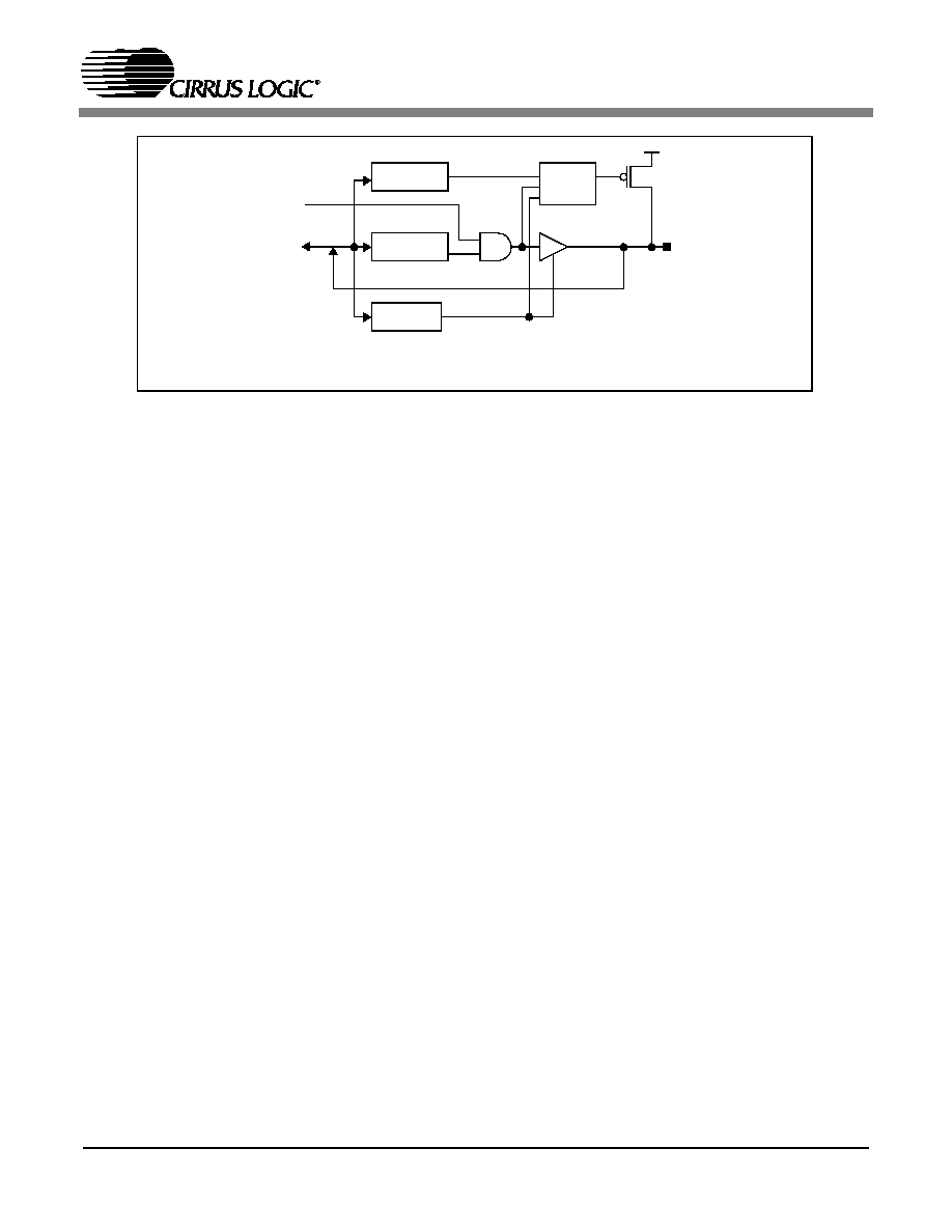
CS5376A
69
19. GENERAL PURPOSE I/O
The General Purpose I/O (GPIO) block provides 12
general purpose pins to interface with external
hardware.
19.1 Pin Descriptions
GPIO[4:0]:CS[4:0] - Pins 32 - 36
Standard GPIO pins also used as SPI 2 chip selects.
GPIO[5:10] - Pins 37, 41 - 45
Standard GPIO pins.
GPIO11:EECS - Pin 46
Standard GPIO pin also used as an SPI 1 chip select
when booting from an external EEPROM.
19.2 GPIO Architecture
Each GPIO pin can be configured as input or out-
put, high or low, with a weak (~200 k
) internal
pull-up resistor enabled or disabled. Several GPIO
pins also double as chip selects for the SPI 1 and
SPI 2 serial ports. Figure 38 shows the structure of
a bi-directional GPIO pin with SPI chip select func-
tionality.
When the CS5376A is used as an SPI master, either
when booting from EEPROM using SPI 1 or per-
forming master mode transactions using SPI 2, the
chip select signals from SPI 1 and SPI 2 are logi-
cally AND-ed with the GPIO data bit. The corre-
sponding GPIO pin should be initialized as output
mode and logical 1 to produce the chip select fall-
ing edge.
19.3 GPIO Registers
When used as standard GPIO pins, settings are pro-
grammed in the GPCFG0 and GPCFG1 registers.
GP_DIR bits set the input/output mode, GP_PULL
bits enable/disable the internal pull-up resistor, and
GP_DATA bits set the output data value. After re-
set, GPIO pins default as inputs with pull-up resis-
tors enabled.
19.4 GPIO Input Mode
When reading a value from the GP_DATA bits, the
returned data reports the current state of the pins. If
a pin is externally driven high it reads a logical 1, if
externally driven low it reads a logical 0. When a
GPIO pin is used as an input, the pull-up resistor
should be disabled to save power if it isn't required.
19.5 GPIO Output Mode
When a GPIO pin is programmed as an output with
a data value of 0, the pin is driven low and the in-
ternal pull-up resistor is automatically disabled.
When programmed as an output with a data value
of 1, the pin is driven high and the pull-up resistor
is inconsequential.
Figure 38. GPIO Bi-directional Structure
CS output from SPI
GPIO/CS
GP_DIR
Data bit
GP_DATA
GP_PULL
Pull Up
Logic
R

CS5376A
70
Any GPIO pin can be used as an open-drain output
by setting the data value to 0, enabling the pull-up,
and using the GP_DIR direction bits to control the
pin value. This open-drain output configuration
uses the internal pull-up resistor to hold the pin
high when GP_DIR is set as an input, and drives the
pin low when GP_DIR is set as an output.
19.5.1 GPIO Reads in Output Mode
When reading GPIO pins the GP_DATA register
value always reports the current state of the pins, so
a value written in output mode does not necessarily
read back the same value. If a pin in output mode is
written as a logical 1, the CS5376A attempts to
drive the pin high. If an external device forces the
pin low, the read value reflects the pin state and re-
turns a logical 0. Similarly, if an output pin is writ-
ten as a logical 0 but forced high externally, the
read value reflects the pin state and returns a logical
1. In both cases the CS5376A is in contention with
the external device resulting in increased power
consumption.
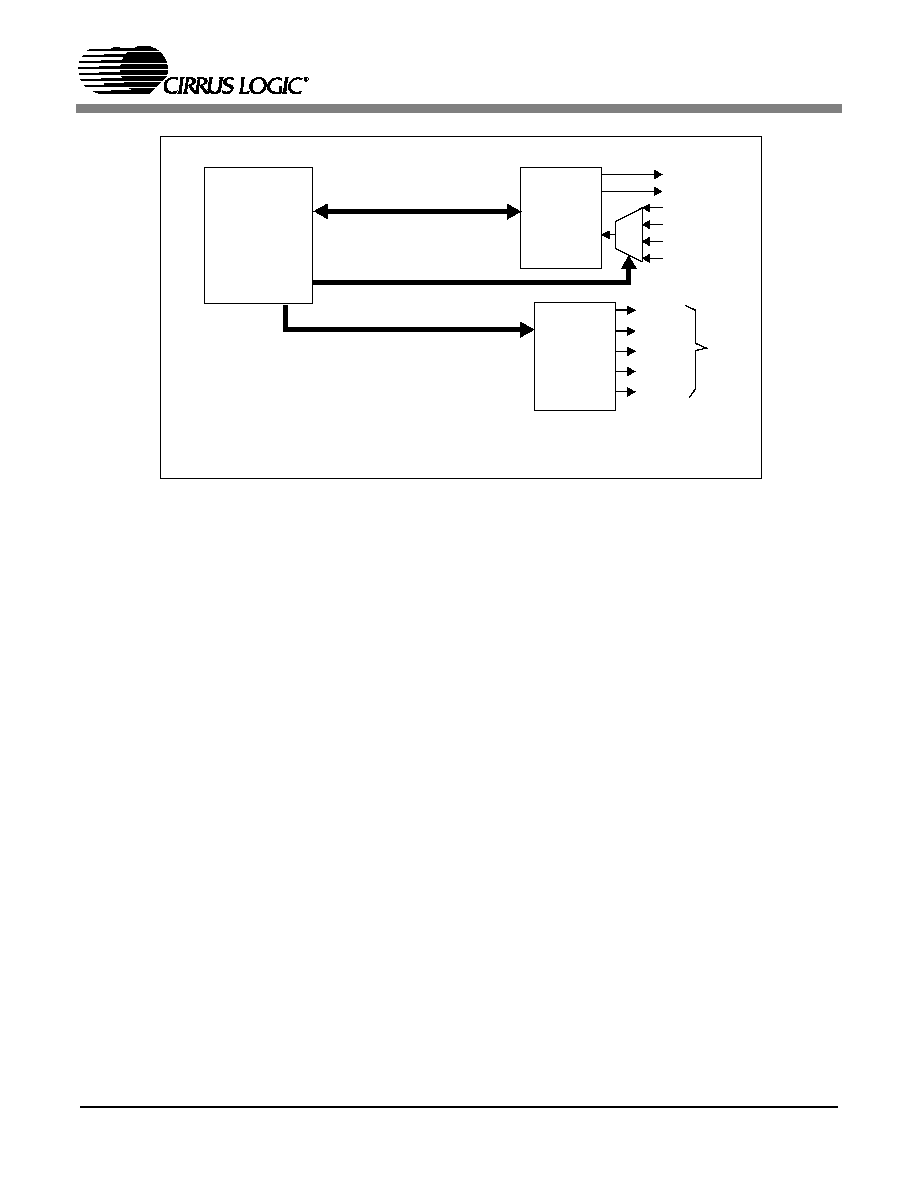
CS5376A
71
20. SERIAL PERIPHERAL INTERFACE 2
The Serial Peripheral Interface 2 (SPI 2) port is a
master mode SPI port designed to interface with se-
rial peripherals. By writing the SPI2 digital filter
registers, multiple serial slave devices can be con-
trolled through the CS5376A.
20.1 Pin Descriptions
CS[4:0] - Pins 32 - 36
Serial chip selects. Multiplexed with GPIO pins.
SCK2 - Pin 31
Serial clock output, common to all channels.
SO - Pin 30
Serial data output, common to all channels.
SI[4:1] - Pins 26 - 29
Serial data inputs.
20.2 SPI 2 Architecture
The SPI 2 pin interface has multiple chip selects
and serial data inputs, but a common serial clock
and serial data output. Which chip select and serial
input to use for a particular slave serial transaction
is selected by bits in the SPI2CTRL digital filter
register.
SPI 2 chip select outputs are multiplexed with
GPIO pins, which cannot perform both functions
simultaneously. When used as a chip select, the
GPIO output must be programmed high to permit
the chip select to operate as an active low signal.
See "General Purpose I/O" on page 69 for informa-
tion about programming the GPIO pins.
The SPI 2 interface transfers data from the SPI 2
registers to a slave serial device and back through a
bi-directional 8-bit shift register. Serial transac-
tions are automatic once control, command, and
data values are written into the SPI 2 digital filter
registers.
20.3 SPI 2 Registers
SPI 2 transactions are initiated by first writing
command, address, and data values to the
SPI2CMD and SPI2DAT digital filter registers,
and then writing the SPI2CTRL register to set the
D2SREQ bit. The D2SREQ bit initiates a serial
Figure 39. Serial Peripheral Interface 2 (SPI 2) Block Diagram
SCK2
SI4
SO
CS1
CS2
CS3
CS4
Pin logic
Select
To
G
P
I
O
B
l
o
c
k
SI2
SI1
SI3
logic
SPI2EN[4:1] / RCH[1:0]
4:1
CS0
Digital
Filter
CS[4:0]
SCKFS[2:0] / SCKPO / SCKPH

CS5376A
72
transaction using the programmed SPI2CTRL con-
figuration.
20.3.1 SPI 2 Control Register
The SPI 2 hardware is configured by the
SPI2CTRL digital filter register (0x10).
Bits in this register select the serial input pin and
chip select pin used for a transaction, set the total
number of bytes in a transaction, initiate a serial
transaction, and report status information about a
transaction. Other bits in SPI2CTRL set hardware
configuration options such as the serial clock rate,
the SPI mode, and the state of internal pull-up re-
sistors.
Chip Select Enable - CS[4:0]
The chip select pin to use during a transaction is se-
lected by the CS0, CS1, CS2, CS3, and CS4 bits.
Multiple chip selects can be enabled to send a
transaction to more than one serial peripheral.
Serial Input Select - SPI2EN[4:1], RCH[1:0]
Which serial input pin will receive data is selected
using the SPI2EN bits and the RCH bits. The
SPI2EN bits enable the serial input, while the RCH
bits select it for the SPI 2 transaction.
A channel's SPI2EN bit should always be enabled,
even when transactions do not expect to receive
data from the slave device.
Transaction Bytes - DNUM[2:0]
DNUM bits specify the total number of bytes to
transfer during a serial transaction, including com-
mand and address bytes. DNUM is zero based and
represents one greater than the number pro-
grammed.
Serial Clock Rate - SCKFS[2:0]
The serial clock rate output from the SCK2 pin is
selected by the SCKFS bits. Serial clock rates
range from 32 kHz to 4.096 MHz.
SPI Mode - SCKPO, SCKPH
The serial mode used for a transaction depends on
the SCKPO and SCKPH bits. The SPI 2 port sup-
ports all four SPI modes, with mode 0 and mode 3
the most commonly used. Supported modes are:
SPI Mode 0 (0,0): SCKPO = 0, SCKPH = 0
SPI Mode 1 (0,1): SCKPO = 0, SCKPH = 1
SPI Mode 2 (1,0): SCKPO = 1, SCKPH = 0
SPI Mode 3 (1,1): SCKPO = 1, SCKPH = 1
Wired-Or Mode - WOM
The SPI 2 pins can operate in two modes depend-
ing on the WOM bit. A default push-pull configu-
ration drives output signals both high and low.
Wired-Or mode only drives low, relying on a weak
internal pull-up resistor to pull the output high.
Wired-Or mode permits multiple serial controllers
to access the same bus without contention.
Initiating Serial Transactions - D2SREQ
Writing the D2SREQ bit starts an SPI 2 serial
transaction. When complete, the D2SREQ bit is au-
tomatically cleared by the SPI 2 hardware.
Status and Error Bits - D2SOP, SWEF, TM
Three bits in the SPI2CTRL register report status
and error information.
D2SOP is set when the SPI 2 port is busy perform-
ing a transaction. It is automatically cleared when
the transaction is completed.
SWEF is set if a request to initiate a new transac-
tion occurs during the current transaction. This flag
is latched and must be cleared manually.
TM is set to indicate the SPI 2 port timed out on the
requested transaction. This flag is latched and must
be cleared manually.
20.3.2 SPI 2 Command Register
The SPI2CMD register (0x11) is a 16-bit digital fil-
ter register with the high byte designated as an SPI

CS5376A
73
command and the low byte designated as an ad-
dress. The high byte holds an 8-bit SPI `write' or
`read' opcode, as shown in Figure 40, and the low
byte holds an 8-bit serial address.
During a transaction, bits in SPI2CMD are output
MSB first, with data in SPI2DAT written or read
following.
20.3.3 SPI 2 Data Register
The SPI2DAT register (0x12) is a 24-bit digital fil-
ter register containing three SPI data bytes. Data in
SPI2DAT is always LSB aligned, with 1-byte data
written or received using the low byte, 2-byte data
written or received using the middle and low bytes,
and 3-byte data written or received using all three
bytes.
Data in SPI2DAT is written or read after writing
the command and address bytes from the
SPI2CMD register.
20.4 SPI 2 Transactions
The SPI 2 port operates as an SPI master to perform
write and read transactions with serial slave periph-
erals. The exact format of the SPI transactions de-
pends on the SPI mode, selected using the SCKPO
and SCKPH bits in the SPI2CTRL register.
Write Transactions
Write transactions start by writing an SPI `write'
(0x02) opcode and an 8-bit destination address into
the SPI2CMD register and the output data value to
the SPI2DAT register. Writing the D2SREQ bit in
the SPI2CTRL register initiates the SPI 2 transac-
tion based on the SPI2CTRL configuration.
A write transaction outputs 1 or 2 bytes from the
SPI2CMD register followed by 1, 2, or 3 bytes
from the SPI2DAT register. Write transactions are
therefore a minimum of 1 byte (DNUM = 0) and a
maximum of 5 bytes (DNUM = 4). The SPI 2 port
uses the DNUM bits in the SPI2CTRL register to
determine the total number of bytes to send during
a write transaction.
Write transactions are not required to use standard
SPI commands. If serial peripherals use non-stan-
dard write commands they can be written into
SPI2CMD and SPI2DAT as required.
Read Transactions
Read transactions start by writing an SPI `read'
(0x03) opcode and an 8-bit source address to the
SPI2CMD register. Writing the D2SREQ bit in the
SPI2CTRL register initiates the SPI 2 transaction
based on the SPI2CTRL configuration, with the
data value automatically received into the
SPI2DAT register.
A read transaction outputs 2 bytes from the
SPI2CMD register and can receive 1, 2, or 3 bytes
into the SPI2DAT register. Read transactions are a
minimum of 3 bytes (DNUM = 2) and a maximum
of 5 bytes (DNUM = 4). The SPI 2 port uses the
DNUM bits in the SPI2CTRL register to determine
the total number of bytes to send and receive during
a read transaction.
Read transactions are not required to use standard
SPI commands. If serial peripherals use non-stan-
dard read commands they can be written to the
SPI2CMD register, as long as they conform to the
format of 2 bytes out with 1, 2, or 3 bytes in.
SPI Modes
The SPI mode for the SPI 2 port is selected in the
SPI2CTRL register using the SCKPO and SCKPH
bits. The most commonly used SPI modes are
mode 0 and mode 3, both of which define the serial
clock with data valid on rising edges and transition-
ing on falling edges.
In SPI mode 0, the SCK2 serial clock is defined ini-
tially in a low state. Output data on the SO pin is
valid immediately after the chip select pin goes
low, and the first rising edge of SCK2 latches valid
data.
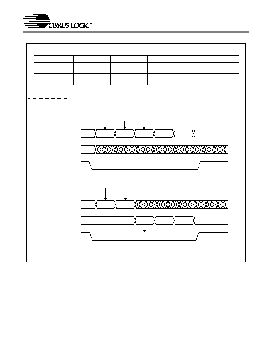
CS5376A
74
In SPI mode 3, the SCK2 serial clock is defined ini-
tially in a high state. Output data on the SO pin is
invalid until the initial falling edge of SCK2, and
the first rising edge of SCK2 latches valid data.
SPI modes 1 and 4 work similarly to modes 0 and
3, with the serial clock defined to have data valid on
falling edges and transitioning on rising edges.
Figure 40. SPI 2 Master Mode Transactions
SO
0x02
ADDR
Data1
SI
SO
SI
SPI 2 Write to External Slave
SPI 2 Read from External Slave
Data3
Data2
0x03
ADDR
Data1
Data3
Data2
CS
CS
SPI2CMD[15:8]
SPI2CMD[7:0]
SPI2DAT
SPI2CMD[15:8]
SPI2CMD[7:0]
SPI2DAT
Instruction
Opcode
Address
Definition
Write
0x02
SPI2CMD[7:0]
Write serial peripheral beginning at the address
given in SPI2CMD[7:0].
Read
0x03
SPI2CMD[7:0]
Read serial peripheral beginning at the address
given in SPI2CMD[7:0].

CS5376A
75
SCK2
SO
Figure 41. SPI 2 Transaction Details
CS
MSB
LSB
SCK2
SI
SCKPO = 0
SCKPO = 1
X
6
1
2
3
4
5
LSB
MSB
6
1
2
3
4
5
1
8
2
7
6
5
4
3
Cycle
Slave devices only drive SI after being selected and responding to a read command.
SCK2
SO
CS
MSB
LSB
SCK2
SI
SCKPO = 0
SCKPO = 1
X
6
1
2
3
4
5
MSB
LSB
6
1
2
3
4
5
1
8
2
7
6
5
4
3
Cycle
Slave devices only drive SI after being selected and responding to a read command.
SPI 2 Transaction with SCKPH=0
SPI 2 Transaction with SCKPH=1

CS5376A
76
21. BOUNDARY SCAN JTAG
The CS5376A includes an IEEE 1149.1 boundary
scan JTAG port to test PCB interconnections. Refer
to the IEEE 1149.1 specification for more informa-
tion about boundary scan testing.
21.1 Pin Descriptions
TRST - Pin 1
Reset input for the test access port (TAP) controller
and all boundary scan cells, active low. Connect to
GND to disable the JTAG port.
TMS - Pin 2
Serial input to select the JTAG test mode.
TCK - Pin 3
Clock input to the TAP controller.
TDI - Pin 4
Serial input to the scan chain or TAP controller.
TDO - Pin 5
Serial output from the scan chain or TAP control-
ler.
21.2 JTAG Architecture
The JTAG test circuitry consists of a test access
port (TAP) controller and boundary scan cells con-
nected to each pin. The boundary scan cells are
linked together to create a scan chain around the
CS5376A.
21.2.1 JTAG Reset
As required by the IEEE 1149.1 specification, the
JTAG TRST signal is independent of the CS5376A
RESET signal. In systems not using the JTAG port,
TRST should be connected to ground. In systems
using the JTAG port, TRST and RESET should be
independently driven to provide reset capability
during boundry scan.
21.2.2 TAP Controller
The test access port (TAP) controller manages
commands and data through the boundary scan
chain. It supports the four JTAG instructions and
contains the IDCODE listed in Table 18.
The TAP controller also implements the 16 JTAG
state assignments from the IEEE 1149.1 specifica-
tion, which are sequenced using TMS and TCK.
Figure 42. JTAG Block Diagram
TDI
TDO
Controller
TAP
TRST
TMS
TCK
Boundary Scan Cells

CS5376A
77
21.2.3 Boundary Scan Cells
The CS5376A JTAG test port provides access to all
device pins via internal boundary scan cells. When
the JTAG port is disabled, boundary scan cells are
transparent and do not affect CS5376A operation.
When the JTAG port is enabled, boundary scan
cells can write and read each pin independent of
CS5376A operation.
Boundary scan cells are serially linked to create a
scan chain around the CS5376A controlled by the
TAP controller. Table 19 lists the scan cell map-
ping of the CS5376A.
JTAG Instructions
Encoding
BYPASS
11
EXTEST
00
IDCODE
01
SAMPLE / PRELOAD
10
JTAG IDCODE
Components
Encoding
Revision
0x10000000
Device ID
0x05376000
Manufacturer ID
0x000000C9
CS5376A IDCODE
0x153760C9
Table 18. JTAG Instructions and IDCODE
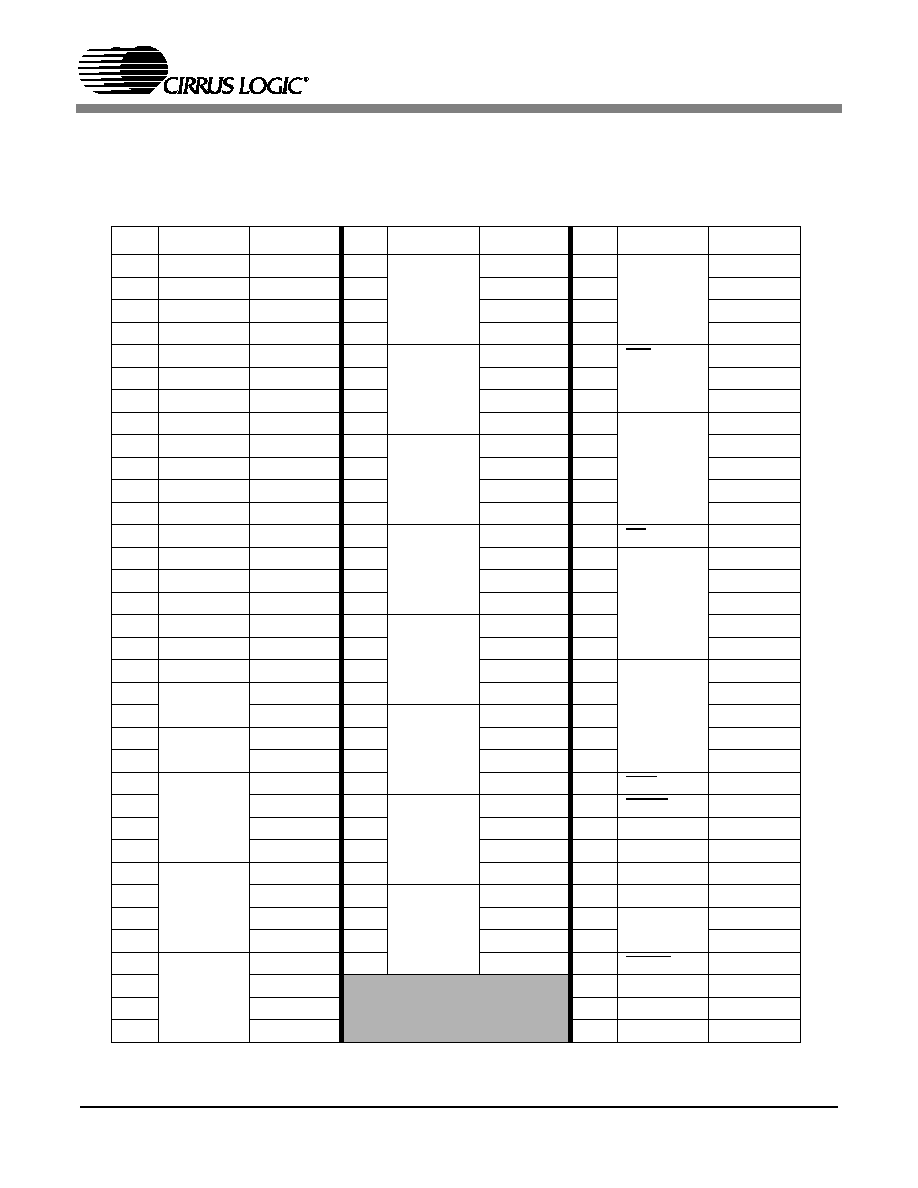
CS5376A
78
BRC
Pin
Function
BRC
Pin
Function
BRC
Pin
Function
1
TBSCLK
data out
36
GPIO3
data in
68
GPIO11
data in
2
TBSDATA
data out
37
data out
69
data out
3
DNC
data out
38
output enable
70
output enable
4
MCLK/2
data out
39
pullup
71
pullup
5
MCLK
data out
40
GPIO4
data in
72
SSO
data out
6
MSYNC
data out
41
data out
73
output enable
7
MDATA4
data in
42
output enable
74
WOM
8
MFLAG4
data in
43
pullup
75
SCK1
data in
9
MDATA3
data in
44
GPIO5
data in
76
data out
10
MFLAG3
data in
45
data out
77
output enable
11
MDATA2
data in
46
output enable
78
WOM
12
MFLAG2
data in
47
pullup
79
pullup
13
MDATA1
data in
48
GPIO6
data in
80
SSI
data in
14
MFLAG1
data in
49
data out
81
MISO
data in
15
GND
data in
50
output enable
82
data out
16
SI4
data in
51
pullup
83
output enable
17
SI3
data in
52
GPIO7
data in
84
WOM
18
SI2
data in
53
data out
85
pullup
19
SI1
data in
54
output enable
86
MOSI
data in
20
SO
data out
55
pullup
87
data out
21
WOM
56
GPIO8
data in
88
output enable
22
SCK2
data out
57
data out
89
WOM
23
WOM
58
output enable
90
pullup
24
GPIO0
data in
59
pullup
91
SINT
data out
25
data out
60
GPIO9
data in
92
RESET
data in
26
output enable
61
data out
93
BOOT
data in
27
pullup
62
output enable
94
TIMEB
data in
28
GPIO1
data in
63
pullup
95
CLK
data in
29
data out
64
GPIO10
data in
96
SYNC
data in
30
output enable
65
data out
97
SDDAT
data out
31
pullup
66
output enable
98
output enable
32
GPIO2
data in
67
pullup
99
SDRDY
data out
33
data out
100
SDCLK
data in
34
output enable
101
SDTKO
data out
35
pullup
102
SDTKI
data in
Table 19. JTAG Scan Cell Mapping

CS5376A
79
22. REVISION HISTORY
The CS5376A is a pin compatible upgrade to the
CS5376. The part family has had three revisions:
CS5376 rev A
CS5376 rev B
CS5376A rev A
The part number change for CS5376A reflects ad-
ditional functionality built into the device.
22.1 Changes from CS5376 rev A to CS5376
rev B
New Sinc Filter, SINC3
Added a new sinc filter, SINC3, between the previ-
ous sinc filters and FIR1. Will permit higher deci-
mation rates for seismology applications. Not used
for 0.25 ms, 0.5 ms, 1 ms, or 2 ms output rates to
maintain backward compatibility.
Added FIR1 Coefficients
Included an improved FIR1 filter to compensate for
sinc filter droop. Previous filter had stop band fre-
quency components up to -100 dB not removed by
the FIR2 brick wall filter. Required stop band at-
tenuation is 130 dB minimum. Previous FIR1 filter
coefficients still included to maintain backwards
compatibility.
Added IIR Coefficients
Included 3 Hz IIR1 and IIR2 filter coefficients for
the 0.5 ms, 1 ms, 2 ms, 3 ms, and 4 ms configura-
tions (5 sets IIR1, 5 sets IIR2). Previous
2 Hz @ 1 ms coefficient set was removed.
Modified Output Word Rate Selection
Changed the DEC bit settings in the FILTCFG reg-
ister used to select an output word rate. Re-num-
bered to include the new 120 Hz, 60 Hz, 30 Hz,
15 Hz, and 7.5 Hz output rates. Other settings the
same for backward compatibility.
Modified ROM Coefficient Selection Method
Changed the ROM coefficient selection routines
(SPI and EEPROM) to require a 24 bit data word.
Previously no data word was required, only the
command byte. The data word is parsed to select
the FIR1, FIR2, IIR1, and IIR2 coefficient sets.
Modified ROM TBS Data Selection Method
Changed the ROM test bit stream selection routine
(SPI and EEPROM) to require a 24 bit data word.
Previously no data word was required, only the
command byte. The data word scales the ROM test
bit stream data to a user selected amplitude.
Modified SPI port to strobe SINT pin
The SPI port now pulses the SINT pin whenever
data is received. Can be used by a microcontroller
to trigger additional data writes. Eliminates the
need to poll the e2dreq bit.
Fixed continuous synchronization operation
The synchronization operation was modified to
permit continuous re-sync. The SD port FIFO is no
longer reset by the SYNC interrupt.
Corrected EEPROM loader bug
The EEPROM loader bug is fixed. A preamble to
write required constants into memory is no longer
required.
22.2 Changes from CS5376 rev B to
CS5376A rev A
Fixed synchronization repeatability bug
Identical synchronization signals previously
caused different impulse responses from multi-
ple devices. Synchronization is now repeatable.

CS5376A
80
Modified SINC2 filter to correct gain and tim-
ing errors
Corrected SINC2 decimate by 2 gain error
which affected 4000 SPS operation. Also mod-
ified SINC2 decimate by 16 output timing to
match output of other SINC2 rates. Previous
SINC2 decimate by 16 output was one sample
later than expected.
Corrected gain error of 333 SPS output rate
SINC architecture was modified to correct gain
error in SINC2 decimate by 12 by moving dec-
imate by 3 stage into SINC3.
Modified SINC3 filter for new low bandwidth
rates.
Newly supported output word rates are 200,
125, 100, 50, 40, 25, 20, 10, 5, 1 SPS. Older low
bandwidth rates of 120, 60, 30, 15, 7.5 SPS
were removed. No changes to 4000, 2000,
1000, 500, 333, 250 SPS rates for backwards
compatibility to CS5376 revision A/B.
Added minimum phase FIR coefficients
Minimum phase FIR1 coefficient set 1 and
FIR2 coefficient set 1 are newly available as se-
lections for the SPI and EEPROM 'Write ROM
Coefficients' command.
Corrected IIR2/IIR3 channels 2, 3, 4 bug
When selecting IIR2 or IIR3 output, data from
channels 2, 3, and 4 were corrupted. IIR2 and
IIR3 now operate correctly for these channels.
Corrected IIR2 coefficient DC offset
IIR2 coefficient sets 0, 1, and 3 did not perfect-
ly cancel DC due to coefficient b20, b21, b22
mismatch. New b21 IIR2 coefficients correct
this offset error.
Removed gain scale factor from 'Write TBS
ROM' command
TBS data was previously scaled during config-
uration by a data word following the 'Write
TBS ROM' command. Added a new TBSGAIN
register (0x2B, replacing WD_CFG) that scales
the TBS amplitude and can be modified during
normal operation.
Removed watchdog timer
The watchdog timer was removed. Replaced
WD_CFG register (0x2B) with TBSGAIN reg-
ister.
Set GPIO11 as tri-state when EEPROM boot
completed
After stand-alone boot from EEPROM,
GPIO11 (acting as EEPROM chip select) was
previously driven high. This pin now tri-states
with an internal pull-up to hold it high.
Modified Test Bit Stream (TBS) to disable
loopback when TBS disabled.
If TBS loopback mode was enabled, the exter-
nal MDATA inputs were disconnected from the
SINC filter even if the TBS was disabled. Now
when the TBS is disabled, loopback mode is
automatically disabled also.
Added Test Bit Stream (TBS) impulse mode.
TBS can now operate in sine wave or impulse
mode, depending on bit 15 in the TBSCFG reg-
ister. When impulse mode is enabled (TBSCFG
bit 15 = 1), a rising edge on the TIMEB pin
causes the TBS to output an impulse bitstream.
When sine wave mode is enabled (TBSCFG bit
15 = 0), operation is identical to CS5376 revi-
sion A/B.

CS5376A
81
Added Test Bit Stream (TBS) synchronization
in sine wave mode.
The TBS sine wave phase will reset if bit 11 of
the TBSCFG register is set (TBSCFG bit 11 =
1) and a rising edge is received on the SYNC
pin. When TBSCFG bit 11 is set low (TBSCFG
bit 11 = 0), TBS phase is unaffected by the
SYNC input similar to CS5376 revision A/B.
Modified Time Break delay function.
The timing delay between receiving a rising
edge on the TIMEB pin and asserting the
TIMEB flag in the output word status bits is
corrected. In CS5376 revision A/B a '0' value in
the TIMEBREAK register (0x29) disabled the
TIMEB status bit write, and a '1' value set the
status bit in the current output word. Now, a '0'
value sets the TIMEB status bit in the current
output word, and a '1' value delays until the fol-
lowing word.

CS5376A
82
23. REGISTER SUMMARY
23.1 SPI 1 Registers
The CS5376A SPI 1 registers interface the serial port to the digital filter.
Name
Addr.
Type
# Bits
Description
SPI1CTRLH
00
R/W
8
SPI 1 Control Register, High Byte
SPI1CTRLM
01
R/W
8
SPI 1 Control Register, Middle Byte
SPI1CTRLL
02
R/W
8
SPI 1 Control Register, Low Byte
SPI1CMDH
03
R/W
8
SPI 1 Command, High Byte
SPI1CMDM
04
R/W
8
SPI 1 Command, Middle Byte
SPI1CMDL
05
R/W
8
SPI 1 Command, Low Byte
SPI1DAT1H
06
R/W
8
SPI 1 Data 1, High Byte
SPI1DAT1M
07
R/W
8
SPI 1 Data 1, Middle Byte
SPI1DAT1L
08
R/W
8
SPI 1 Data 1, Low Byte
SPI1DAT2H
09
R/W
8
SPI 1 Data 2, High Byte
SPI1DAT2M
0A
R/W
8
SPI 1 Data 2, Middle Byte
SPI1DAT2L
0B
R/W
8
SPI 1 Data 2, Low Byte
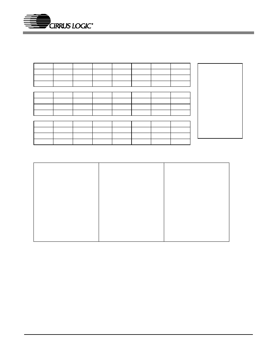
CS5376A
83
23.1.1
SPI1CTRL : 0x00, 0x01, 0x02
(MSB) 23
22
21
20
19
18
17
16
--
--
--
--
--
--
--
--
R/W
R/W1
R/W
R/W
R/W
R/W
R/W
R/W
0
0
0
0
1
0
1
1
15
14
13
12
11
10
9
8
SMODF
--
--
EMOP
SWEF
--
--
E2DREQ
R
R/W
R
R
R
R/W
R/W
R/W
0
0
0
0
0
0
1
0
7
6
5
4
3
2
1
(LSB) 0
--
--
--
--
--
--
--
--
R/W
R/W
R/W
R/W
R/W
R/W
R/W
R/W
0
0
1
0
0
0
0
0
SPI 1 Address: 0x00
0x01
0x02
--
Not defined;
read as 0
R
Readable
W
Writable
R/W
Readable and
Writable
Bits in bottom rows
are reset condition
Bit definitions:
23:16 --
reserved
15
SMODF
SPI 1 mode fault flag
7:0
--
reserved
14:13 --
reserved
12
EMOP
External master to SPI 1
operation in progress
flag
11
SWEF
SPI 1 write collision
error flag
10:9
--
reserved
8
E2DREQ External master to digital
filter request flag
Figure 43. SPI 1 Control Register SPI1CTRL
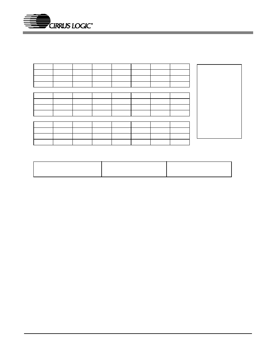
CS5376A
84
23.1.2
SPI1CMD : 0x03, 0x04, 0x05
(MSB) 23
22
21
20
19
18
17
16
S1CMD23
S1CMD22
S1CMD21
S1CMD20
S1CMD19
S1CMD18
S1CMD17
S1CMD16
R/W
R/W
R/W
R/W
R/W
R/W
R/W
R/W
0
0
0
0
0
0
0
0
15
14
13
12
11
10
9
8
S1CMD15
S1CMD14
S1CMD13
S1CMD12
S1CMD11
S1CMD10
S1CMD9
S1CMD8
R/W
R/W
R/W
R/W
R/W
R/W
R/W
R/W
0
0
0
0
0
0
0
0
7
6
5
4
3
2
1
(LSB) 0
S1CMD7
S1CMD6
S1CMD5
S1CMD4
S1CMD3
S1CMD2
S1CMD1
S1CMD0
R/W
R/W
R/W
R/W
R/W
R/W
R/W
R/W
0
0
0
0
0
0
0
0
SPI 1 Address: 0x03
0x04
0x05
--
Not defined;
read as 0
R
Readable
W
Writable
R/W
Readable and
Writable
Bits in bottom rows
are reset condition
Figure 44. SPI 1 Command Register SPI1CMD
Bit definitions:
23:16 S1CMD[23:16] SPI 1 Command
High Byte
15:8
S1CMD[15:8] SPI 1 Command
Middle Byte
15:8
S1CMD[7:0] SPI 1 Command
Low Byte

CS5376A
85
23.1.3
SPI1DAT1 : 0x06, 0x07, 0x08
(MSB) 23
22
21
20
19
18
17
16
S1DAT23
S1DAT22
S1DAT21
S1DAT20
S1DAT19
S1DAT18
S1DAT17
S1DAT16
R/W
R/W
R/W
R/W
R/W
R/W
R/W
R/W
0
0
0
0
0
0
0
0
15
14
13
12
11
10
9
8
S1DAT15
S1DAT14
S1DAT13
S1DAT12
S1DAT11
S1DAT10
S1DAT9
S1DAT8
R/W
R/W
R/W
R/W
R/W
R/W
R/W
R/W
0
0
0
0
0
0
0
0
7
6
5
4
3
2
1
(LSB) 0
S1DAT7
S1DAT6
S1DAT5
S1DAT4
S1DAT3
S1DAT2
S1DAT1
S1DAT0
R/W
R/W
R/W
R/W
R/W
R/W
R/W
R/W
0
0
0
0
0
0
0
0
SPI 1 Address: 0x06
0x07
0x08
--
Not defined;
read as 0
R
Readable
W
Writable
R/W
Readable and
Writable
Bits in bottom rows
are reset condition
Figure 45. SPI 1 Data Register SPI1DAT1
Bit definitions:
23:16 S1DAT[23:16] SPI 1 Data
High Byte
15:8
S1DAT[15:8] SPI 1 Data
Middle Byte
15:8
S1DAT[7:0]
SPI 1 Data
Low Byte

CS5376A
86
23.1.4
SPI1DAT2 : 0x09, 0x0A, 0x0B
(MSB) 23
22
21
20
19
18
17
16
S1DAT23
S1DAT22
S1DAT21
S1DAT20
S1DAT19
S1DAT18
S1DAT17
S1DAT16
R/W
R/W
R/W
R/W
R/W
R/W
R/W
R/W
0
0
0
0
0
0
0
0
15
14
13
12
11
10
9
8
S1DAT15
S1DAT14
S1DAT13
S1DAT12
S1DAT11
S1DAT10
S1DAT9
S1DAT8
R/W
R/W
R/W
R/W
R/W
R/W
R/W
R/W
0
0
0
0
0
0
0
0
7
6
5
4
3
2
1
(LSB) 0
S1DAT7
S1DAT6
S1DAT5
S1DAT4
S1DAT3
S1DAT2
S1DAT1
S1DAT0
R/W
R/W
R/W
R/W
R/W
R/W
R/W
R/W
0
0
0
0
0
0
0
0
SPI 1 Address: 0x09
0x0A
0x0B
--
Not defined;
read as 0
R
Readable
W
Writable
R/W
Readable and
Writable
Bits in bottom rows
are reset condition
Figure 46. SPI 1 Data Register SPI1DAT2
Bit definitions:
23:16 S1DAT[23:16] SPI 1 Data
High Byte
15:8
S1DAT[15:8] SPI 1 Data
Middle Byte
15:8
S1DAT[7:0]
SPI 1 Data
Low Byte
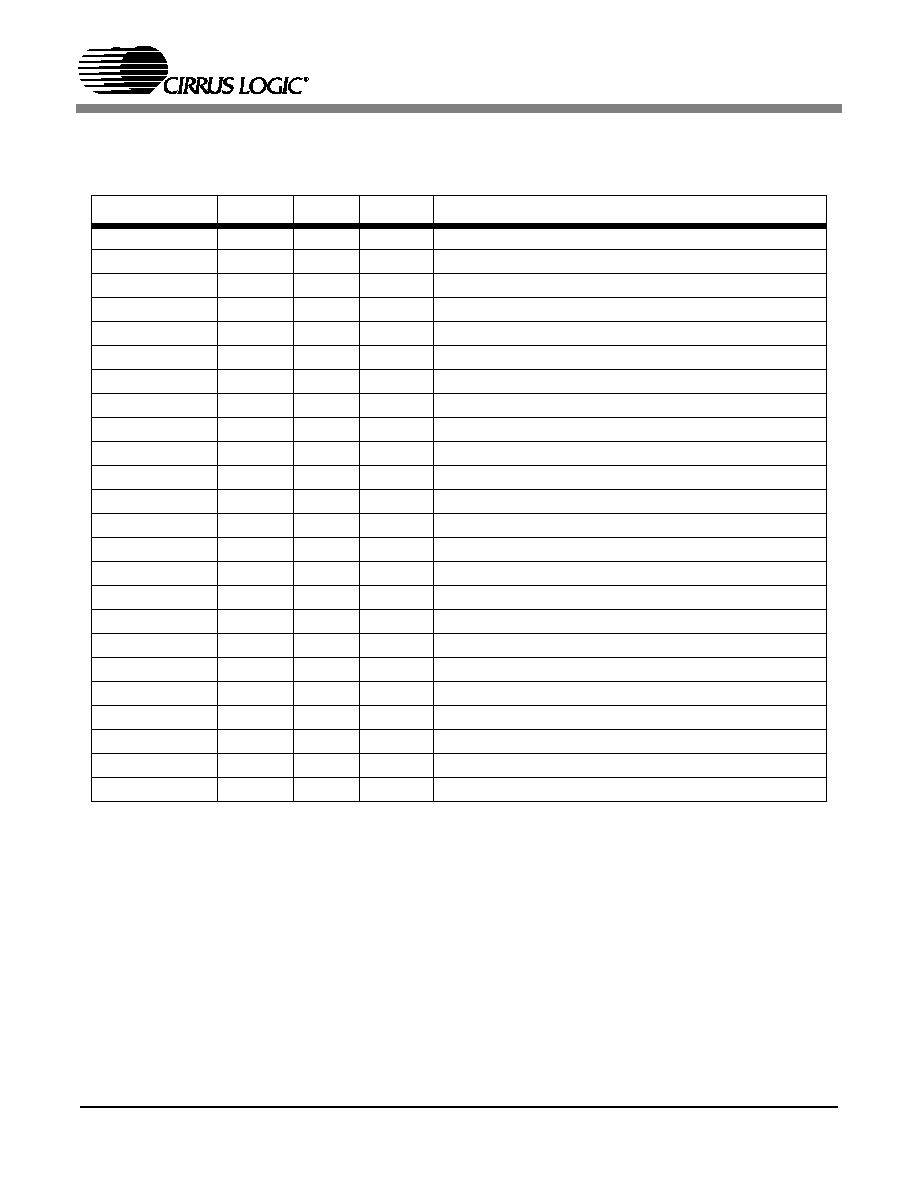
CS5376A
87
23.2
Digital Filter Registers
The CS5376A digital filter registers control hardware peripherals and filtering functions.
Name
Addr.
Type
# Bits
Description
CONFIG
00
R/W
24
Hardware Configuration
RESERVED
01-0D
R/W
24
Reserved
GPCFG0
0E
R/W
24
GPIO[7:0] Direction, Pull-Up Enable, and Data
GPCFG1
0F
R/W
24
GPIO[11:8] Direction, Pull-Up Enable, and Data
SPI2CTRL
10
R/W
24
SPI2 Control
SPI2CMD
11
R/W
16
SPI2 Command
SPI2DAT
12
R/W
24
SPI2 Data
RESERVED
13-1F
R/W
24
Reserved
FILTCFG
20
R/W
24
Digital Filter Configuration
GAIN1
21
R/W
24
Gain Correction Channel 1
GAIN2
22
R/W
24
Gain Correction Channel 2
GAIN3
23
R/W
24
Gain Correction Channel 3
GAIN4
24
R/W
24
Gain Correction Channel 4
OFFSET1
25
R/W
24
Offset Correction Channel 1
OFFSET2
26
R/W
24
Offset Correction Channel 2
OFFSET3
27
R/W
24
Offset Correction Channel 3
OFFSET4
28
R/W
24
Offset Correction Channel 4
TIMEBRK
29
R/W
24
Time Break Delay
TBSCFG
2A
R/W
24
Test Bit Stream Configuration
TBSGAIN
2B
R/W
24
Test Bit Stream Gain
SYSTEM1
2C
R/W
24
User Defined System Register 1
SYSTEM2
2D
R/W
24
User Defined System Register 2
VERSION
2E
R/W
24
Hardware Version ID
SELFTEST
2F
R/W
24
Self-Test Result Code
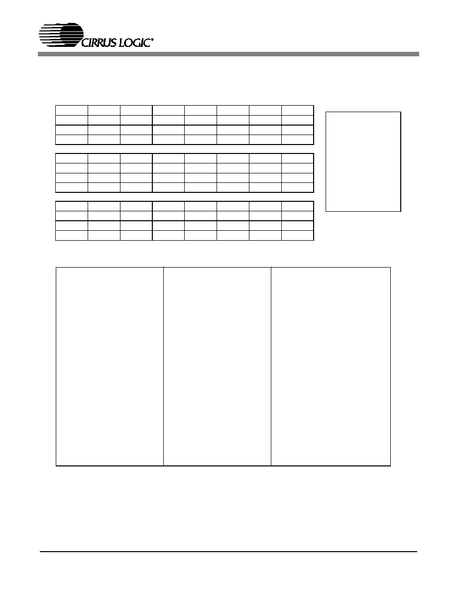
CS5376A
88
23.2.1
CONFIG : 0x00
(MSB)23
22
21
20
19
18
17
16
--
--
--
--
--
DFS2
DFS1
DFS0
R/W
R/W
R/W
R/W
R/W
R/W
R/W
R/W
0
0
0
0
0
1
0
1
15
14
13
12
11
10
9
8
--
--
--
--
--
MCKFS2
MCKFS1
MCKFS0
R/W
R/W
R/W
R/W
R/W
R/W
R/W
R/W
0
0
0
0
0
1
0
0
7
6
5
4
3
2
1
(LSB)0
--
--
MCKEN2
MCKEN
MDIFS
--
BOOT
MSEN
R/W
R/W
R/W
R/W
R/W
R/W
R
R/W
0
0
0
0
0
0
0
1
Figure 47. Hardware Configuration Register CONFIG
Bit definitions:
23:19 --
reserved
15:11 --
reserved
7:6
--
reserved
18:16 DFS
[2:0]
Digital filter
frequency select
111: 16.384 MHz
110: 8.192 MHz
101: 4.096 MHz
100: 2.048 MHz
011: 1.024 MHz
010: 512 kHz
001: 256 kHz
000: 32 kHz
10:8
MCKFS
[2:0]
MCLK frequency select
111: reserved
110: reserved
101: 4.096 MHz
100: 2.048 MHz
011: 1.024 MHz
010: 512 kHz
001: reserved
000: reserved
5
MCKEN2
MCLK/2 output enable
1: Enabled
0: Disabled
4
MCKEN
MCLK output enable
1: Enabled
0: Disabled
3
MDIFS
MDATA input frequency
select
1: 256 kHz
0: 512 kHz
2
--
reserved
1
BOOT
Boot source indicator
1: Booted from EEPROM
0: Booted from Micro
0
MSEN
MSYNC enable
1: MSYNC generated
0: MSYNC remains low
DF Address: 0x00
--
Not defined;
read as 0
R
Readable
W
Writable
R/W
Readable and
Writable
Bits in bottom rows
are reset condition

CS5376A
89
23.2.2
GPCFG0 : 0x0E
(MSB) 23
22
21
20
19
18
17
16
GP_DIR7
GP_DIR6
GP_DIR5
GP_DIR4
GP_DIR3
GP_DIR2
GP_DIR1
GP_DIR0
R/W
R/W
R/W
R/W
R/W
R/W
R/W
R/W
0
0
0
0
0
0
0
0
15
14
13
12
11
10
9
8
GP_PULL7
GP_PULL6
GP_PULL5
GP_PULL4
GP_PULL3
GP_PULL2
GP_PULL1
GP_PULL0
R/W
R/W
R/W
R/W
R/W
R/W
R/W
R/W
1
1
1
1
1
1
1
1
7
6
5
4
3
2
1
(LSB) 0
GP_DATA7
GP_DATA6
GP_DATA5
GP_DATA4
GP_DATA3
GP_DATA2
GP_DATA1
GP_DATA0
R/W
R/W
R/W
R/W
R/W
R/W
R/W
R/W
1
1
1
1
1
1
1
1
DF Address: 0x0E
--
Not defined;
read as 0
R
Readable
W
Writable
R/W
Readable and
Writable
Bits in bottom rows
are reset condition
Bit
definitions:
Note: GPIO[4:0] also used as SPI 2 chip selects CS[4:0].
23:16 GP_DIR
[7:0]
GPIO pin direction
1: Output
0: Input
15:8
GP_PULL
[7:0]
GPIO pullup resistor
1: Enabled
0: Disabled
7:0
GP_DATA
[7:0]
GPIO data value
1: VDD
0: GND
Figure 48. GPIO Configuration Register GPCFG0

CS5376A
90
23.2.3
GPCFG1 : 0x0F
(MSB) 23
22
21
20
19
18
17
16
--
--
--
--
GP_DIR11
GP_DIR10
GP_DIR9
GP_DIR8
R/W
R/W
R/W
R/W
R/W
R/W
R/W
R/W
0
0
0
0
0
0
0
0
15
14
13
12
11
10
9
8
--
--
--
--
GP_PULL11
GP_PULL10
GP_PULL9
GP_PULL8
R/W
R/W
R/W
R/W
R/W
R/W
R/W
R/W
0
0
0
0
1
1
1
1
7
6
5
4
3
2
1
(LSB) 0
--
--
--
--
GP_DATA11
GP_DATA10
GP_DATA9
GP_DATA8
R/W
R/W
R/W
R/W
R/W
R/W
R/W
R/W
0
0
0
0
1
1
1
1
DF Address: 0x0F
--
Not defined;
read as 0
R
Readable
W
Writable
R/W
Readable and
Writable
Bits in bottom rows
are reset condition
Bit definitions:
Note: GPIO11 also used as boot EEPROM chip select EECS.
23:20 --
reserved
15:12 --
reserved
7:4
--
reserved
19:16 GP_DIR
[11:8]
GPIO pin direction
1: Output
0: Input
11:8
GP_PULL
[11:8]
GPIO pullup resistor
1: Enabled
0: Disabled
3:0
GP_DATA
[11:8]
GPIO data value
1: VDD
0: GND
Figure 49. GPIO Configuration Register GPCFG1
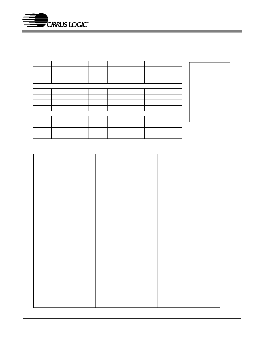
CS5376A
91
23.2.4
SPI2CTRL : 0x10
(MSB) 23
22
21
20
19
18
17
16
WOM
SCKFS2
SCKFS1
SCKFS0
SPI2EN3
SPI2EN2
SPI2EN1
SPI2EN0
R/W
R/W
R/W
R/W
R/W
R/W
R/W
R/W
0
0
1
1
1
1
1
1
15
14
13
12
11
10
9
8
RCH1
RCH0
D2SOP
SCKPH
SWEF
SCKPO
TM
D2SREQ
R/W
R/W
R
R/W
R/W
R/W
R/W
R/W
0
0
0
0
0
0
0
0
7
6
5
4
3
2
1
(LSB) 0
DNUM2
DNUM1
DNUM0
CS4
CS3
CS2
CS1
CS0
R/W
R/W
R/W
R/W
R/W
R/W
R/W
R/W
1
1
1
0
0
0
0
0
DF Address: 0x10
--
Not defined;
read as 0
R
Readable
W
Writable
R/W
Readable
and Writable
Bits in bottom rows
are reset condition.
Bit definitions:
23
WOM
Wired-or mode
1: Enabled (open drain)
0: Disabled (push-pull)
15:14 RCH
[1:0]
Read channel
11: SI4
10: SI3
01: SI2
00: SI1
7:5
DNUM
[2:0]
Number of bytes in
serial transaction
22:20 SCKFS
[2:0]
SCK2 frequency select
111: reserved
110: reserved
101: 4.096 MHz
100: 2.048 MHz
011: 1.024 MHz
010: 512 kHz
001: 128 kHz
000: 32 kHz
13
D2SOP
Digital filter to SPI2
operation in progress
flag
4
CS4
Chip Select 4 Enable
12
SCKPH
SO output timing
1: Data becomes valid
on first SCK2 edge
0: Data becomes valid
before first SCK2 edge
3
CS3
Chip Select 3 Enable
2
CS2
Chip Select 2 Enable
11
SWEF
SPI2 write collision flag 1
CS1
Chip Select 1 Enable
19:16 SPI2EN
[3:0]
SI[4:1] input enable
1111: All enabled
0000: All disabled
10
SCKPO
SCK2 data polarity
1: Valid on falling edge,
transition on rising edge
0: Valid on rising edge,
transition on falling edge
0
CS0
Chip Select 0 Enable
9
TM
SPI2 timeout flag
1: SPI2 timed out
0: not timed out
8
D2SREQ Digital filter to SPI2
serial transaction request
1: Request operation
0: Operation complete
(cleared by hardware)
Figure 50. SPI 2 Control Register SPI2CTRL

CS5376A
92
23.2.5
SPI2CMD : 0x11
(MSB) 23
22
21
20
19
18
17
16
--
--
--
--
--
--
--
--
R/W
R/W
R/W
R/W
R/W
R/W
R/W
R/W
0
0
0
0
0
0
0
0
15
14
13
12
11
10
9
8
SCMD15
SCMD14
SCMD13
SCMD12
SCMD11
SCMD10
SCMD9
SCMD8
R/W
R/W
R/W
R/W
R/W
R/W
R/W
R/W
0
0
0
0
0
0
0
0
7
6
5
4
3
2
1
(LSB) 0
SCMD7
SCMD6
SCMD5
SCMD4
SCMD3
SCMD2
SCMD1
SCMD0
R/W
R/W
R/W
R/W
R/W
R/W
R/W
R/W
0
0
0
0
0
0
0
0
DF Address: 0x11
--
Not defined;
read as 0
R
Readable
W
Writable
R/W
Readable and
Writable
Bits in bottom rows
are reset condition
Bit definitions:
23:16 --
reserved
15:8
SCMD[15:8] SPI2 Upper Command
Byte
15:8
SCMD[7:0]
SPI2 Lower Command
Byte
Figure 51. SPI 2 Command Register SPI2CMD

CS5376A
93
23.2.6
SPI2DAT : 0x12
(MSB) 23
22
21
20
19
18
17
16
SDAT23
SDAT22
SDAT21
SDAT20
SDAT19
SDAT18
SDAT17
SDAT16
R/W
R/W
R/W
R/W
R/W
R/W
R/W
R/W
0
0
0
0
0
0
0
0
15
14
13
12
11
10
9
8
SDAT15
SDAT14
SDAT13
SDAT12
SDAT11
SDAT10
SDAT9
SDAT8
R/W
R/W
R/W
R/W
R/W
R/W
R/W
R/W
0
0
0
0
0
0
0
0
7
6
5
4
3
2
1
(LSB) 0
SDAT7
SDAT6
SDAT5
SDAT4
SDAT3
SDAT2
SDAT1
SDAT0
R/W
R/W
R/W
R/W
R/W
R/W
R/W
R/W
0
0
0
0
0
0
0
0
DF Address: 0x12
--
Not defined;
read as 0
R
Readable
W
Writable
R/W
Readable and
Writable
Bits in bottom rows
are reset condition
Figure 52. SPI 2 Data Register SPI2DAT
Bit definitions:
23:16 SDAT[23:16]
SPI2 Upper Data
Byte
15:8
SDAT[15:8]
SPI2 Middle Data
Byte
15:8
SDAT[7:0]
SPI2 Lower Data
Byte

CS5376A
94
23.2.7
FILTCFG : 0x20
(MSB) 23
22
21
20
19
18
17
16
--
--
--
EXP4
EXP3
EXP2
EXP1
EXP0
R/W
R/W
R/W
R/W
R/W
R/W
R/W
R/W
0
0
0
0
0
0
0
0
15
14
13
12
11
10
9
8
--
ORCAL
USEOR
USEGR
--
FSEL2
FSEL1
FSEL0
R/W
R/W
R/W
R/W
R/W
R/W
R/W
R/W
0
0
0
0
0
0
0
0
7
6
5
4
3
2
1
(LSB) 0
DEC3
DEC2
DEC1
DEC0
--
--
CH1
CH0
R/W
R/W
R/W
R/W
R/W
R/W
R/W
R/W
0
0
0
0
0
0
0
0
DF Address: 0x20
--
Not defined;
read as 0
R
Readable
W
Writable
R/W
Readable and
Writable
Bits in bottom rows
are reset condition
Bit definitions:
23:21 --
reserved
15
--
reserved
7:4
DEC[3:0]
Decimation selection
(Output word rate)
20:16 EXP[4:0] OFFSET calibration
exponent
14
ORCAL
Run OFFSET calibration
1: Enable
0: Disable
0111: 4000 SPS
0110: 2000 SPS
0101: 1000 SPS
0100: 500 SPS
0011: 333 SPS
13
USEOR
Use OFFSET correction
1: Enable
0: Disable
0010: 250 SPS
0001: 200 SPS
0000: 125 SPS
1111: 100 SPS
1110: 50 SPS
12
USEGR
Use GAIN correction
1: Enable
0: Disable
1101: 40 SPS
1100: 25 SPS
1011: 20 SPS
1010: 10 SPS
1001: 5 SPS
1000: 1 SPS
11
--
reserved
3:2
--
reserved
10:8
FSEL[2:0] Output filter stage select
111: reserved
110: reserved
101: IIR 3rd Order
100: IIR 2nd Order
011: IIR 1st Order
010: FIR2 Output
001: FIR1 Output
000: SINC Output
1:0
CH[1:0]
Channel Enable
11: 3 Channel (1, 2, 3)
10: 2 Channel (1, 2)
01: 1 Channel (1 only)
00: 4 Channel (1, 2, 3, 4)
Figure 53. Filter Configuration Register FILTCFG
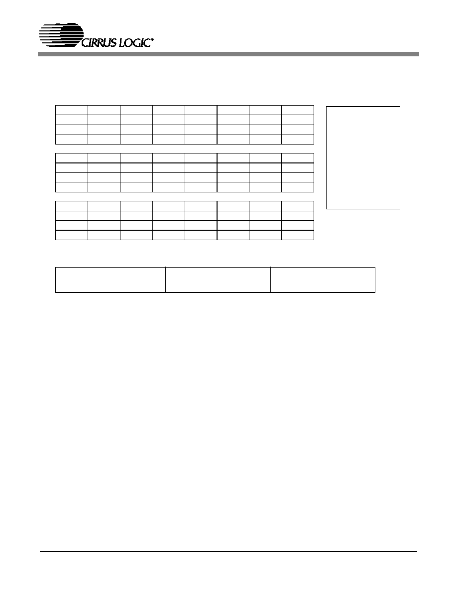
CS5376A
95
23.2.8
GAIN1 - GAIN4 : 0x21 - 0x24
(MSB) 23
22
21
20
19
18
17
16
GAIN23
GAIN22
GAIN21
GAIN20
GAIN19
GAIN18
GAIN17
GAIN16
R/W
R/W
R/W
R/W
R/W
R/W
R/W
R/W
0
0
0
0
0
0
0
0
15
14
13
12
11
10
9
8
GAIN15
GAIN14
GAIN13
GAIN12
GAIN11
GAIN10
GAIN9
GAIN8
R/W
R/W
R/W
R/W
R/W
R/W
R/W
R/W
0
0
0
0
0
0
0
0
7
6
5
4
3
2
1
(LSB) 0
GAIN7
GAIN6
GAIN5
GAIN4
GAIN3
GAIN2
GAIN1
GAIN0
R/W
R/W
R/W
R/W
R/W
R/W
R/W
R/W
0
0
0
0
0
0
0
0
DF Address: 0x21
--
Not defined;
read as 0
R
Readable
W
Writable
R/W
Readable and
Writable
Bits in bottom rows
are reset condition
Figure 54. Gain Correction Register GAIN1
Bit definitions:
23:16 GAIN[23:16]
Gain Correction
Upper Byte
15:8
GAIN[15:8]
Gain Correction
Middle Byte
15:8
GAIN[7:0]
Gain Correction
Lower Byte

CS5376A
96
23.2.9
OFFSET1 - OFFSET4 : 0x25 - 0x28
(MSB) 23
22
21
20
19
18
17
16
OFST23
OFST22
OFST21
OFST20
OFST19
OFST18
OFST17
OFST16
R/W
R/W
R/W
R/W
R/W
R/W
R/W
R/W
0
0
0
0
0
0
0
0
15
14
13
12
11
10
9
8
OFST15
OFST14
OFST13
OFST12
OFST11
OFST10
OFST9
OFST8
R/W
R/W
R/W
R/W
R/W
R/W
R/W
R/W
0
0
0
0
0
0
0
0
7
6
5
4
3
2
1
(LSB) 0
OFST7
OFST6
OFST5
OFST4
OFST3
OFST2
OFST1
OFST0
R/W
R/W
R/W
R/W
R/W
R/W
R/W
R/W
0
0
0
0
0
0
0
0
DF Address: 0x25
--
Not defined;
read as 0
R
Readable
W
Writable
R/W
Readable and
Writable
Bits in bottom rows
are reset condition
Figure 55. Offset Correction Register OFFSET1
Bit definitions:
23:16 OFST[23:16]
Offset Correction
Upper Byte
15:8
OFST[15:8]
Offset Correction
Middle Byte
15:8
OFST[7:0]
Offset Correction
Lower Byte

CS5376A
97
23.2.10
TIMEBRK : 0x29
(MSB) 23
22
21
20
19
18
17
16
TBRK23
TBRK22
TBRK21
TBRK20
TBRK19
TBRK18
TBRK17
TBRK16
R/W
R/W
R/W
R/W
R/W
R/W
R/W
R/W
0
0
0
0
0
0
0
0
15
14
13
12
11
10
9
8
TBRK15
TBRK14
TBRK13
TBRK12
TBRK11
TBRK10
TBRK9
TBRK8
R/W
R/W
R/W
R/W
R/W
R/W
R/W
R/W
0
0
0
0
0
0
0
0
7
6
5
4
3
2
1
(LSB) 0
TBRK7
TBRK6
TBRK5
TBRK4
TBRK3
TBRK2
TBRK1
TBRK0
R/W
R/W
R/W
R/W
R/W
R/W
R/W
R/W
0
0
0
0
0
0
0
0
DF Address: 0x29
--
Not defined;
read as 0
R
Readable
W
Writable
R/W
Readable and
Writable
Bits in bottom rows
are reset condition
Figure 56. Time Break Counter Register TIMEBRK
Bit definitions:
23:16 TBRK[23:16] Time Break Counter
Upper Byte
15:8
TBRK[15:8] Time Break Counter
Middle Byte
15:8
TBRK[7:0]
Time Break Counter
Lower Byte
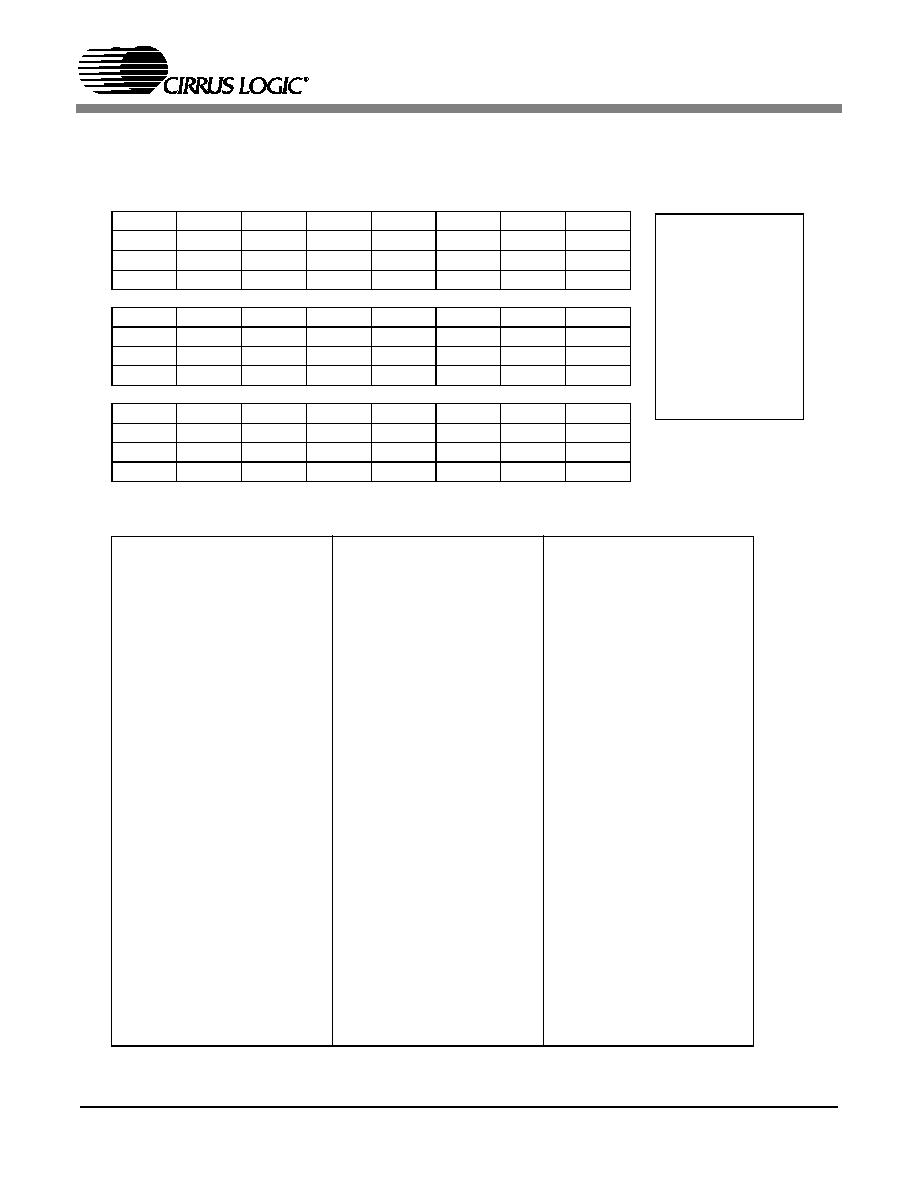
CS5376A
98
23.2.11
TBSCFG : 0x2A
(MSB) 23
22
21
20
19
18
17
16
INTP7
INTP6
INTP5
INTP4
INTP3
INTP2
INTP1
INTP0
R/W
R/W
R/W
R/W
R/W
R/W
R/W
R/W
0
0
0
0
0
0
0
0
15
14
13
12
11
10
9
8
TMODE
RATE2
RATE1
RATE0
TSYNC
CDLY2
CDLY1
CDLY0
R/W
R/W
R/W
R/W
R/W
R/W
R/W
R/W
0
0
0
0
0
0
0
0
7
6
5
4
3
2
1
(LSB) 0
LOOP
RUN
DDLY5
DDLY4
DDLY3
DDLY2
DDLY1
DDLY0
R/W
R/W
R/W
R/W
R/W
R/W
R/W
R/W
0
0
0
0
0
0
0
0
DF Address: 0x2A
--
Not defined;
read as 0
R
Readable
W
Writable
R/W
Readable and
Writable
Bits in bottom rows
are reset condition
Figure 57. Test Bit Stream Configuration Register TBSCFG
Bit definitions:
23:16 INTP[7:0]
Interpolation factor
0xFF: 256
0xFE: 255
...
0x01: 2
0x00: 1 (use once)
15
TMODE
Operational mode
1: Impulse mode
0: Sine Mode
7
LOOP
Loopback
TBSDATA output
to MDATA inputs
1: Enabled
0: Disabled
14:12 RATE[2:0]
TBSDATA and
TBSCLK output
rate.
111: 2.048 MHz
110: 1.024 MHz
101: 512 kHz
100: 256 kHz
011: 128 kHz
010: 64 kHz
001: 32 kHz
000: 4 kHz
6
RUN
Run Test Bit Stream
1: Enabled
0: Disabled
11
TSYNC
Synchronization
1: Sync enabled
0: No sync
10:8
CDLY[2:0]
TBSCLK output
phase delay
111: 7/8 period
110: 3/4 period
101: 5/8 period
100: 1/2 period
011: 3/8 period
010: 1/4 period
001: 1/8 period
000: none
5:0
DDLY[5:0]
TBSDATA output
delay
0x3F: 63 bits
0x3E: 62 bits
...
0x01: 1 bit
0x00: 0 bits ( no
delay)

CS5376A
99
23.2.12
TBSGAIN : 0x2B
(MSB) 23
22
21
20
19
18
17
16
TGAIN23
TGAIN22
TGAIN21
TGAIN20
TGAIN19
TGAIN18
TGAIN17
TGAIN16
R/W
R/W
R/W
R/W
R/W
R/W
R/W
R/W
0
0
0
0
0
0
0
0
15
14
13
12
11
10
9
8
TGAIN15
TGAIN14
TGAIN13
TGAIN12
TGAIN11
TGAIN10
TGAIN9
TGAIN8
R/W
R/W
R/W
R/W
R/W
R/W
R/W
R/W
0
0
0
0
0
0
0
0
7
6
5
4
3
2
1
(LSB) 0
TGAIN7
TGAIN6
TGAIN5
TGAIN4
TGAIN3
TGAIN2
TGAIN1
TGAIN0
R/W
R/W
R/W
R/W
R/W
R/W
R/W
R/W
0
0
0
0
0
0
0
0
DF Address: 0x2B
--
Not defined;
read as 0
R
Readable
W
Writable
R/W
Readable and
Writable
Bits in bottom rows
are reset condition
Figure 58. Test Bit Stream Gain Register TBSGAIN
Bit definitions:
23:16 TGAIN[23:16] Test Bit Stream Gain
Upper Byte
15:8
TGAIN[15:8] Test Bit Stream
Gain Middle Byte
15:8
TGAIN[7:0] Test Bit Stream
Gain Lower Byte

CS5376A
100
23.2.13
SYSTEM1, SYSTEM2 : 0x2C, 0x2D
(MSB) 23
22
21
20
19
18
17
16
SYS23
SYS22
SYS21
SYS20
SYS19
SYS18
SYS17
SYS16
R/W
R/W
R/W
R/W
R/W
R/W
R/W
R/W
0
0
0
0
0
0
0
0
15
14
13
12
11
10
9
8
SYS15
SYS14
SYS13
SYS12
SYS11
SYS10
SYS9
SYS8
R/W
R/W
R/W
R/W
R/W
R/W
R/W
R/W
0
0
0
0
0
0
0
0
7
6
5
4
3
2
1
(LSB) 0
SYS7
SYS6
SYS5
SYS4
SYS3
SYS2
SYS1
SYS0
R/W
R/W
R/W
R/W
R/W
R/W
R/W
R/W
0
0
0
0
0
0
0
0
DF Address: 0x2C
--
Not defined;
read as 0
R
Readable
W
Writable
R/W
Readable and
Writable
Bits in bottom rows
are reset condition
Figure 59. User Defined System Register SYSTEM1
Bit definitions:
23:16 SYS[23:16]
System Register
Upper Byte
15:8
SYS[15:8]
System Register
Middle Byte
15:8
SYS[7:0]
System Register
Lower Byte

CS5376A
101
23.2.14
VERSION : 0x2E
(MSB) 23
22
21
20
19
18
17
16
TYPE7
TYPE6
TYPE5
TYPE4
TYPE3
TYPE2
TYPE1
TYPE0
R/W
R/W
R/W
R/W
R/W
R/W
R/W
R/W
0
1
1
1
0
1
1
0
15
14
13
12
11
10
9
8
HW7
HW6
HW5
HW4
HW3
HW2
HW1
HW0
R/W
R/W
R/W
R/W
R/W
R/W
R/W
R/W
0
0
0
0
0
0
0
1
7
6
5
4
3
2
1
(LSB) 0
ROM7
ROM6
ROM5
ROM4
ROM3
ROM2
ROM1
ROM0
R/W
R/W
R/W
R/W
R/W
R/W
R/W
R/W
0
0
0
0
0
0
0
1
DF Address: 0x2E
--
Not defined;
read as 0
R
Readable
W
Writable
R/W
Readable and
Writable
Bits in bottom rows
are reset condition
Figure 60. Hardware Version ID Register VERSION
Bit definitions:
23:16 TYPE
[7:0]
Chip Type
76 - CS5376, CS5376A
15:8
HW
[7:0]
Hardware Revision
01 - CS5376 Rev A
02 - CS5376 Rev B
03 - CS5376A Rev A
7:4
ROM
[7:0]
ROM Version
01 - Ver 1.0
02 - Ver 2.0
03 - Ver 3.0

CS5376A
102
23.2.15
SELFTEST : 0x2F
(MSB) 23
22
21
20
19
18
17
16
--
--
--
--
EU3
EU2
EU1
EU0
R/W
R/W
R/W
R/W
R/W
R/W
R/W
R/W
0
0
0
0
1
0
1
0
15
14
13
12
11
10
9
8
DRAM3
DRAM2
DRAM1
DRAM0
PRAM3
PRAM2
PRAM1
PRAM0
R/W
R/W
R/W
R/W
R/W
R/W
R/W
R/W
1
0
1
0
1
0
1
0
7
6
5
4
3
2
1
(LSB) 0
DROM3
DROM2
DROM1
DROM0
PROM3
PROM2
PROM1
PROM0
R/W
R/W
R/W
R/W
R/W
R/W
R/W
R/W
1
0
1
0
1
0
1
0
DF Address: 0x2F
--
Not defined;
read as 0
R
Readable
W
Writable
R/W
Readable and
Writable
Bits in bottom rows
are reset condition
Figure 61. Self Test Result Register SELFTEST
Bit definitions:
23:20 --
reserved
15:12 DRAM
[3:0]
Data RAM Test
`A': Pass
`F': Fail
7:4
DROM
[3:0]
Data ROM Test
`A': Pass
`F': Fail
19:16 EU
[3:0]
Execution Unit Test
`A': Pass
`F': Fail
11:8
PRAM
[3:0]
Program RAM Test
`A': Pass
`F': Fail
3:0
PROM
[3:0]
Program ROM Test
`A': Pass
`F': Fail
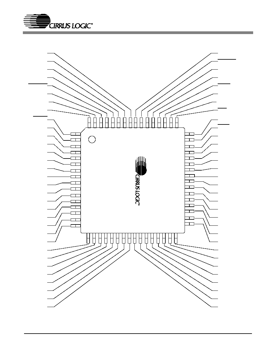
CS5376A
103
24. PIN DESCRIPTIONS
TIMEB
CLK
SYNC
SDDAT
SDRDY
SDCLK
SDTKO
SDTKI
TRST
TMS
TCK
TDI
TDO
GND
VD
TBSCLK
TBSDATA
DNC
VDD2
MCLK/2
MCLK
MSYNC
MDATA4
MFLAG4
MDATA3
MFLAG3
MDATA2
MFLAG2
MDATA1
MFLAG1
GND
GND2
BOOT
RESET
VDD1
GND1
SINT
MOSI
MISO
SSI
SCK1
SSO
GPIO11:EECS
GPIO10
GPIO9
GPIO8
GPIO7
GPIO6
VD
GND
GND2
GPIO5
GPIO4:CS4
GPIO3:CS3
GPIO2:CS2
GPIO1:CS1
GPIO0:CS0
SCK2
SO
SI1
SI2
SI3
SI4
VDD2
1
2
3
4
5
6
7
8
9
10
11
12
13
14
15
16
17 18 19 20 21 22 23 2425 26 2728 29 30 3132
33
34
35
36
37
38
39
40
41
42
43
44
45
46
47
48
49
50
51
52
53
54
55
56
57
58
59
60
61
62
63
64
CS5
376A
6
4
-
P
I
N
TQ
FP

CS5376A
104
Pin
Name
Pin
Number
Pin
Type
Pin
Description
JTAG port
TRST
1
Input
JTAG reset, active low.
Connect to GND if JTAG is not used.
TMS
2
Input
JTAG test mode select.
TCK
3
Input
JTAG clock input.
TDI
4
Input
JTAG data input.
TDO
5
Output
JTAG data output.
Test Bit Stream
TBSCLK
8
Output
Test bit stream clock output.
TBSDATA
9
Output
Test bit stream data output.
No Connect
DNC
10
N/A
Do not connect.
Modulator Interface
MCLK/2
12
Output
Modulator clock output, half rate.
MCLK
13
Output
Modulator clock output, full rate.
MSYNC
14
Output
Modulator sync output.
MDATA[4:1]
15, 17, 19, 21
Input
Modulator data inputs.
MFLAG[4:1]
16, 18, 20, 22
Input
Modulator flag inputs.
Serial Peripheral Interface 2
SI[4:1]
26, 27, 28, 29
Input
SPI 2 data inputs.
SO
30
Output
SPI 2 data output.
SCK2
31
Output
SPI 2 clock output.
General Purpose Input / Output
GPIO[0:4]:CS[0:4]
32, 33, 34,
35, 36
Input / Output
General Purpose I/O with SPI 2 chip selects.
GPIO[5:10]
37, 41, 42,
43, 44, 45
Input / Output
General Purpose I/O.
GPIO11:EECS
46
Input / Output
General Purpose I/O with boot EEPROM chip select.
Serial Peripheral Interface 1
47
Output
SPI 1 slave select output, active low.
SCK1
48
Input / Output
SPI 1 serial clock input / output.
49
Input
SPI 1 slave select input, active low.
MISO
50
Input / Output
SPI 1 data, master in / slave out.
Open drain output requiring a 10 k
pull-up.
MOSI
51
Input / Output
SPI 1 data, master out / slave in.
52
Output
SPI 1 serial interrupt output, active low.
Reset Control
55
Input
Reset, active low.
BOOT
56
Input
Boot mode select.
Time Break
TIMEB
57
Input
Time break input.
SSO
SSI
SINT
RESET
CS5376A
105
Clock and Synchronization
CLK
58
Input
Clock input, nominal 32.768 MHz.
SYNC
59
Input
Sync input.
Serial Data Port
SDDAT
60
Output
SD port data output.
SDRDY
61
Output
SD port data ready, active low.
Open drain output requiring a 10 k
pull-up.
SDCLK
62
Input
SD port clock input.
SDTKO
63
Output
SD port token output.
SDTKI
64
Input
SD port token input.
Power Supplies
VDD1
54
Supply
Pin power supply for pins 1 - 5 and 41 - 64.
VDD2
11, 25
Supply
Pin power supplies for pins 8 - 37.
VD
7, 40
Supply
Logic core power supplies.
GND1, GND2, GND
6, 23, 24,
38, 39, 53
Supply
Digital grounds.
Pin
Name
Pin
Number
Pin
Type
Pin
Description
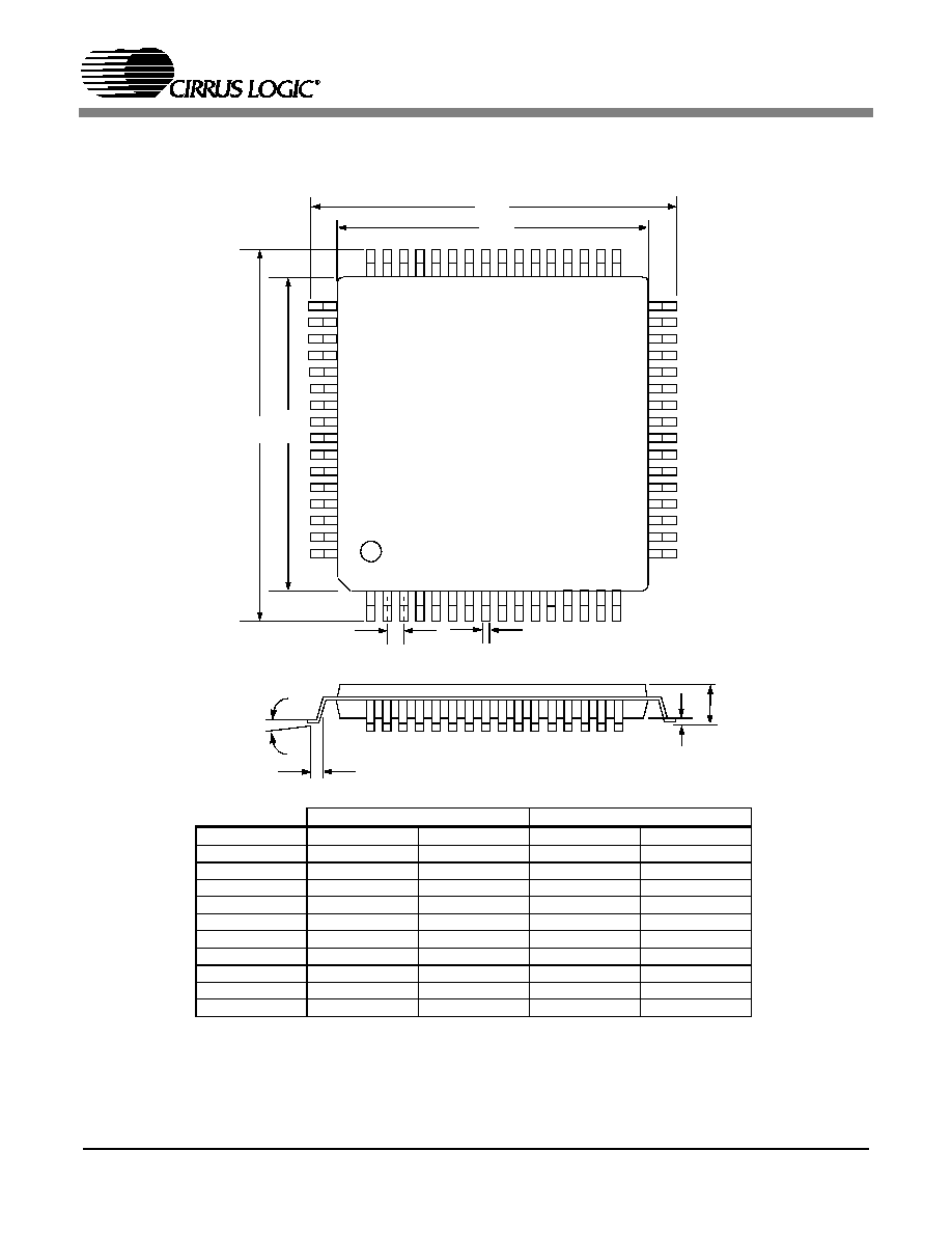
CS5376A
106
25. PACKAGE DIMENSIONS
INCHES
MILLIMETERS
DIM
MIN
MAX
MIN
MAX
A
---
0.063
---
1.60
A1
0.002
0.006
0.05
0.15
B
0.007
0.011
0.17
0.27
D
0.461
0.484
11.70
12.30
D1
0.390
0.398
9.90
10.10
E
0.461
0.484
11.70
12.30
E1
0.390
0.398
9.90
10.10
e*
0.016
0.024
0.40
0.60
L
0.018
0.030
0.45
0.75
�
0.000�
7.000�
0.00�
7.00�
* Nominal pin pitch is 0.50 mm
Controlling dimension is mm.
JEDEC Designation: MS026
64L TQFP PACKAGE DRAWING
E1
E
D1
D
1
e
L
B
A1
A

CS5376A
107
26. DOCUMENT REVISIONS
Revision
Date
Changes
PP1
September 2003 Initial "Preliminary Product" release.
F1
February 2004
Update group delay on page 50, power consumption on page 14 and MISO read
timing on page 15. Add TBS impulse data on page 66 and MOSI pull-up on
page 32.
Contacting Cirrus Logic Support
For all product questions and inquiries contact a Cirrus Logic Sales Representative.
To find one nearest you go to
www.cirrus.com
IMPORTANT NOTICE
Cirrus Logic, Inc. and its subsidiaries ("Cirrus") believe that the information contained in this document is accurate and reliable. However, the information is
subject to change without notice and is provided "AS IS" without warranty of any kind (express or implied). Customers are advised to obtain the latest version
of relevant information to verify, before placing orders, that information being relied on is current and complete. All products are sold subject to the terms and
conditions of sale supplied at the time of order acknowledgment, including those pertaining to warranty, patent infringement, and limitation of liability. No re-
sponsibility is assumed by Cirrus for the use of this information, including use of this information as the basis for manufacture or sale of any items, or for in-
fringement of patents or other rights of third parties. This document is the property of Cirrus and by furnishing this information, Cirrus grants no license, express
or implied under any patents, mask work rights, copyrights, trademarks, trade secrets or other intellectual property rights. Cirrus owns the copyrights associated
with the information contained herein and gives consent for copies to be made of the information only for use within your organization with respect to Cirrus
integrated circuits or other products of Cirrus. This consent does not extend to other copying such as copying for general distribution, advertising or promotional
purposes, or for creating any work for resale.
CERTAIN APPLICATIONS USING SEMICONDUCTOR PRODUCTS MAY INVOLVE POTENTIAL RISKS OF DEATH, PERSONAL INJURY, OR SEVERE
PROPERTY OR ENVIRONMENTAL DAMAGE ("CRITICAL APPLICATIONS"). CIRRUS PRODUCTS ARE NOT DESIGNED, AUTHORIZED OR WARRANT-
ED FOR USE IN AIRCRAFT SYSTEMS, MILITARY APPLICATIONS, PRODUCTS SURGICALLY IMPLANTED INTO THE BODY, LIFE SUPPORT PROD-
UCTS OR OTHER CRITICAL APPLICATIONS (INCLUDING MEDICAL DEVICES, AIRCRAFT SYSTEMS OR COMPONENTS AND PERSONAL OR
AUTOMOTIVE SAFETY OR SECURITY DEVICES). INCLUSION OF CIRRUS PRODUCTS IN SUCH APPLICATIONS IS UNDERSTOOD TO BE FULLY AT
THE CUSTOMER'S RISK AND CIRRUS DISCLAIMS AND MAKES NO WARRANTY, EXPRESS, STATUTORY OR IMPLIED, INCLUDING THE IMPLIED
WARRANTIES OF MERCHANTABILITY AND FITNESS FOR PARTICULAR PURPOSE, WITH REGARD TO ANY CIRRUS PRODUCT THAT IS USED IN
SUCH A MANNER. IF THE CUSTOMER OR CUSTOMER'S CUSTOMER USES OR PERMITS THE USE OF CIRRUS PRODUCTS IN CRITICAL APPLICA-
TIONS, CUSTOMER AGREES, BY SUCH USE, TO FULLY INDEMNIFY CIRRUS, ITS OFFICERS, DIRECTORS, EMPLOYEES, DISTRIBUTORS AND OTH-
ER AGENTS FROM ANY AND ALL LIABILITY, INCLUDING ATTORNEYS' FEES AND COSTS, THAT MAY RESULT FROM OR ARISE IN CONNECTION
WITH THESE USES.
Cirrus Logic, Cirrus, and the Cirrus Logic logo designs are trademarks of Cirrus Logic, Inc. All other brand and product names in this document may be trade-
marks or service marks of their respective owners.