
1
Copyright
©
Cirrus Logic, Inc. 2004
(All Rights Reserved)
Cirrus Logic, Inc.
http://www.cirrus.com
CS5460A
Single Phase Bi-Directional Power/Energy IC
Features
Energy Data Linearity: ±0.1% of Reading
over 1000:1 Dynamic Range.
On-Chip Functions: (Real) Energy, I
V,
I
RMS
and V
RMS
, Energy-to-Pulse
Conversion
Smart "Auto-Boot" Mode from Serial
EEPROM Enables Use without MCU.
AC or DC System Calibration
Mechanical Counter/Stepper Motor Driver
Meets Accuracy Spec for IEC 687/1036, JIS
Typical Power Consumption <12 mW
Interface Optimized for Shunt Sensor
V vs. I Phase Compensation
Ground-Referenced Signals with Single
Supply
On-chip 2.5 V Reference (MAX 60 ppm/∞C
drift)
Simple Three-Wire Digital Serial Interface
Watch Dog Timer
Power Supply Monitor
Power Supply Configurations
VA+ = +5 V; VA- = 0 V; VD+ = +3.3 V to +5 V
Description
The CS5460A is a highly integrated power mea-
surement solution which combines two
Analog-to-Digital Converters (ADCs), high speed
power calculation functions, and a serial interface
on a single chip. It is designed to accurately mea-
sure and calculate: Real (True) Energy,
Instantaneous Power, I
RMS
, and V
RMS
for single
phase 2- or 3-wire power metering applications.
The CS5460A interfaces to a low-cost shunt resis-
tor or transformer to measure current, and to a
resistive divider or potential transformer to mea-
sure voltage. The CS5460A features a
bi-directional serial interface for communication
with a micro-controller and a pulse output engine
for which the average pulse frequency is propor-
tional to the real power. The CS5460A has on-chip
functionality to facilitate AC or DC system-level
calibration.
The "Auto-Boot" feature allows the CS5460A to
function `stand-alone' and to initialize itself on sys-
tem power-up. In Auto-Boot Mode, the CS5460A
reads the calibration data and start-up instructions
from an external EEPROM. In this mode, the
CS5460A can operate without a microcontroller, in
order to lower the total bill-of-materials cost.
PGA
x10,x50
VA+
VD+
IIN+
IIN-
VIN+
VIN-
VREFIN
VREFOUT
VA-
XIN
XOUT CPUCLK
DGND
CS
SDO
SDI
SCLK
INT
EOUT
Digital
Filter
High Pass
Filter
Voltage
Reference
System
Clock
/K
Clock
Generator
Serial
Interface
Power
Calculation
Engine
(Energy
I * V
I
,V
)
RMS
RMS
Energy-to-
Pulse
Converter
Power
Monitor
PFMON
x1
x10
4
Order
Modulator
th
RESET
Digital
Filter
Calibration
SRAM
EDIR
High Pass
Filter
2
Order
Modulator
nd
Watch Dog
Timer
MODE
Control /
SEP `04
DS487F2

CS5460A
2
TABLE OF CONTENTS
1. CHARACTERISTICS AND SPECIFICATIONS ........................................................................ 5
ANALOG CHARACTERISTICS ................................................................................................ 5
VREFOUT REFERENCE OUTPUT VOLTAGE........................................................................ 7
5V DIGITAL CHARACTERISTICS............................................................................................ 7
3.3 V DIGITAL CHARACTERISTICS........................................................................................ 8
ABSOLUTE MAXIMUM RATINGS ........................................................................................... 8
SWITCHING CHARACTERISTICS .......................................................................................... 9
2. GENERAL DESCRIPTION ..................................................................................................... 12
2.1 Theory of Operation ......................................................................................................... 12
2.1.1 DS Modulators ................................................................................................... 12
2.1.2 High-Rate Digital Low-Pass Filters ..................................................................... 12
2.1.3 Digital Compensation Filters ............................................................................... 12
2.1.4 Digital High-Pass Filters ...................................................................................... 12
2.1.5 Overall Filter Response ....................................................................................... 13
2.1.6 Gain and DC Offset Adjustment .......................................................................... 13
2.1.7 Real Energy and RMS Computations ................................................................. 13
2.2 Performing Measurements ............................................................................................... 13
2.2.1 CS5460A Linearity Performance ......................................................................... 15
2.2.2 Single Computation Cycle (C=0) ......................................................................... 15
2.2.3 Continuous Computation Cycles (C=1) ............................................................... 16
2.3 Basic Application Circuit Configurations .......................................................................... 16
3. FUNCTIONAL DESCRIPTION ............................................................................................... 21
3.1 Pulse-Rate Output ........................................................................................................... 21
3.2 Pulse Output for Normal Format, Stepper Motor Format and Mechanical Counter Format 22
3.2.1 Normal Format .................................................................................................... 22
3.2.2 Mechanical Counter Format ................................................................................ 23
3.2.3 Stepper Motor Format ......................................................................................... 23
3.3 Auto-Boot Mode Using EEPROM .................................................................................... 24
3.3.1 Auto-Boot Configuration ...................................................................................... 24
3.3.2 Auto-Boot Data for EEPROM .............................................................................. 25
3.3.3 Application Note AN225 ...................................................................................... 26
3.4 Interrupt and Watchdog Timer ......................................................................................... 26
3.4.1 Interrupt ............................................................................................................... 26
3.4.1.1 Clearing the Status Register ............................................................... 26
3.4.1.2 Typical use of the INT pin ................................................................... 26
3.4.1.3 INT Active State .................................................................................. 26
3.4.1.4 Exceptions ........................................................................................... 26
3.4.2 Watch Dog Timer ................................................................................................ 26
3.5 Oscillator Characteristics ................................................................................................. 27
3.6 Analog Inputs ................................................................................................................... 27
3.7 Voltage Reference ........................................................................................................... 27
3.8 Calibration ........................................................................................................................ 27
3.8.1 Overview of Calibration Process ......................................................................... 27
3.8.2 The Calibration Registers .................................................................................... 28
3.8.3 Calibration Sequence .......................................................................................... 28
3.8.4 Calibration Signal Input Level ............................................................................. 29
3.8.5 Calibration Signal Frequency .............................................................................. 29
3.8.6 Input Configurations for Calibrations ................................................................... 29
3.8.7 Description of Calibration Algorithms .................................................................. 30
3.8.7.1 AC Offset Calibration Sequence ......................................................... 30
3.8.7.2 DC Offset Calibration Sequence ......................................................... 31
3.8.7.3 AC Gain Calibration Sequence ........................................................... 31

CS5460A
3
3.8.7.4 DC Gain Calibration Sequence ......................................................... 31
3.8.8 Duration of Calibration Sequence ....................................................................... 31
3.9 Phase Compensation ...................................................................................................... 31
3.10 Time-Base Calibration Register ..................................................................................... 32
3.11 Power Offset Register ................................................................................................... 32
3.12 Input Protection - Current Limit ...................................................................................... 32
3.13 Input Filtering ................................................................................................................. 34
3.14 Protection Against High-Voltage and/or High-Current Surges ...................................... 37
3.15 Improving RFI Immunity ................................................................................................ 38
3.16 PCB Layout ................................................................................................................... 38
4. SERIAL PORT OVERVIEW .................................................................................................... 38
4.1 Commands (Write Only) .................................................................................................. 39
4.2 Serial Port Interface ......................................................................................................... 42
4.3 Serial Read and Write ..................................................................................................... 42
4.3.1 Register Write ..................................................................................................... 42
4.3.2 Register Read ..................................................................................................... 42
4.4 System Initialization ......................................................................................................... 42
4.5 Serial Port Initialization .................................................................................................... 43
4.6 CS5460A Power States ................................................................................................... 43
5. REGISTER DESCRIPTION ................................................................................................... 44
5.1 Configuration Register ...................................................................................................... 44
5.2 Current Channel DC Offset Register and Voltage Channel DC Offset Register .............. 46
5.3 Current Channel Gain Register and Voltage Channel Gain Register............................... 46
5.4 Cycle Count Register........................................................................................................ 46
5.5 Pulse-Rate Register ......................................................................................................... 47
5.6 I,V,P,E Signed Output Register Results ........................................................................... 47
5.7 IRMS, VRMS Unsigned Output Register Results ............................................................. 47
5.8 Timebase Calibration Register ......................................................................................... 47
5.9 Power Offset Register ...................................................................................................... 48
5.10 Current Channel AC Offset Register and Voltage Channel AC Offset Register............. 48
5.11 Status Register and Mask Register ................................................................................ 48
5.12 Control Register.............................................................................................................. 50
6. PIN DESCRIPTION ................................................................................................................. 51
7. PACKAGE DIMENSIONS ...................................................................................................... 53
8. ORDERING INFORMATION .................................................................................................. 54
9. CHANGE HISTORY ................................................................................................................ 54

CS5460A
4
LIST OF FIGURES
Figure 1. CS5460A Read and Write Timing Diagrams.................................................................. 10
Figure 2. CS5460A Auto-Boot Sequence Timing .......................................................................... 11
Figure 3. Data Flow. ...................................................................................................................... 13
Figure 4. Voltage Input Filter Characteristics ................................................................................ 14
Figure 5. Current Input Filter Characteristics ................................................................................ 14
Figure 6. Typical Connection Diagram (One-Phase 2-Wire, Direct Connect to Power Line) ........ 17
Figure 7. Typical Connection Diagram (One-Phase 2-Wire, Isolated from Power Line) ............... 18
Figure 8. Typical Connection Diagram (One-Phase 3-Wire) ......................................................... 19
Figure 9. Typical Connection Diagram (One-Phase 3-Wire - No Neutral Available)..................... 20
Figure 10. Time-plot representation of pulse output for a typical burst of pulses (Normal Format)23
Figure 11. Mechanical Counter Format on EOUT and EDIR ........................................................ 23
Figure 12. Stepper Motor Format on EOUT and EDIR ................................................................. 24
Figure 13. Typical Interface of EEPROM to CS5460A .................................................................. 24
Figure 14. Timing Diagram for Auto-Boot Sequence .................................................................... 25
Figure 15. Oscillator Connection ................................................................................................... 27
Figure 16. System Calibration of Gain. ......................................................................................... 30
Figure 17. System Calibration of Offset. ....................................................................................... 30
Figure 18. Calibration Data Flow................................................................................................... 30
Figure 19. Example of AC Gain Calibration .................................................................................. 31
Figure 20. Input Protection for Single-Ended Input Configurations ............................................... 37
Figure 21. CS5460A Register Diagram ......................................................................................... 44
LIST OF TABLES
Table 1. Differential Input Voltage vs. Output Code ...................................................................... 14
Table 2. Available range of ±0.1% output linearity, with default settings in the gain/offset registers.15
Table 3. Default Register Values upon Reset Event ..................................................................... 43
CS5460A
5
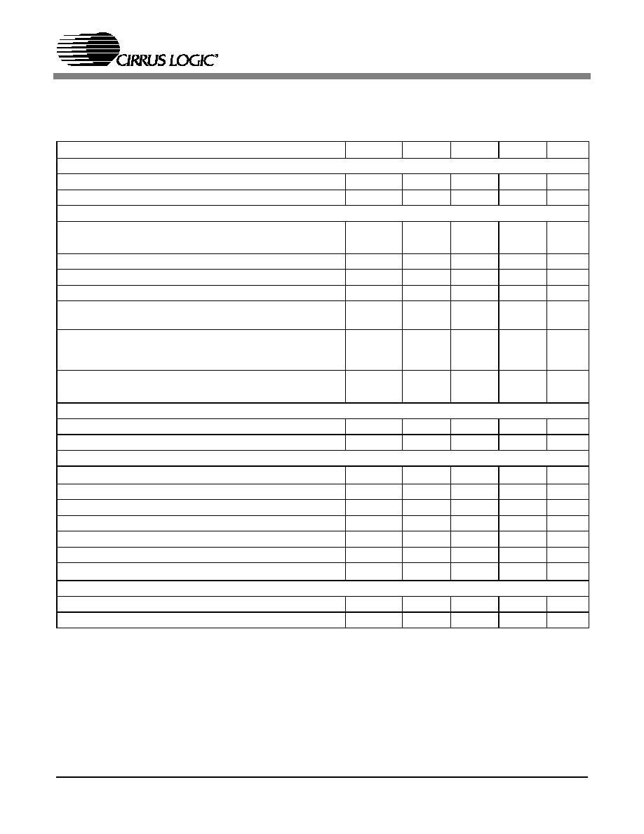
1. CHARACTERISTICS AND SPECIFICATIONS
ANALOG CHARACTERISTICS
(T
A
= -40 ∞C to +85 ∞C; VA+ = VD+ = +5 V ±10%; VREFIN = +2.5 V; VA- = AGND = 0 V; MCLK = 4.096 MHz,
K = 1; N = 4000 ==> OWR = 4000 Sps.)(See Notes 1, 2, 3, 4, and 5.)
Notes:
1.
Bipolar Offset Errors and Full-Scale Gain Errors for the current and voltage channels refer to the respective Irms
Register and Vrms Register output, when the device is operating in `continuous computation cycles' data acquisition
mode,
after offset/gain system calibration sequences have been executed. These specs do not apply to the error
of the Instantaneous Current/Voltage Register output.
2.
Specifications guaranteed by design, characterization, and/or test.
3.
Analog signals are relative to VA- and digital signals to DGND unless otherwise noted.
4.
In requiring VA+ = VD+ =5 V ±10%, note that it is allowable for VA+, VD+ to differ by as much as ±200 mV, as long
as VA+ > VD+.
5.
Note that "Sps" is an abbreviation for units of "samples per second".
6.
Effective Input Impedance (Zin) is determined by clock frequency (DCLK) and Input Capacitance (IC).
Zin = 1/(IC*DCLK/4). Note that DCLK = MCLK / K.
Parameter
Symbol Min Typ
Max
Unit
Accuracy (Both Channels)
Common Mode Rejection
(DC, 50, 60 Hz)
CMRR
80
-
-
dB
Offset Drift (Without the High Pass Filter)
-
5
-
nV/∞C
Analog Inputs (Current Channel)
Maximum Differential Input Voltage Range
(Gain = 10)
{(V
IIN+
) - (V
IIN-
)}
(Gain = 50)
I
IN
-
-
-
-
500
100
mV
P-P
mV
P-P
Total Harmonic Distortion
THD
I
80
-
-
dB
Common Mode + Signal on IIN+ or IIN-
(Gain = 10 or 50)
-0.25
-
VA+
V
Crosstalk with Voltage Channel at Full Scale
(50, 60 Hz)
-
-
-115
dB
Input Capacitance
(Gain = 10)
(Gain = 50)
C
in
-
-
25
25
-
-
pF
pF
Effective Input Impedance
(Note 6)
(Gain = 10)
(Gain = 50)
Z
inI
Z
inI
-
-
30
30
-
-
k
k
Noise (Referred to Input)
(Gain = 10)
(Gain = 50)
-
-
-
-
20
4
µV
rms
µV
rms
Accuracy (Current Channel)
Bipolar Offset Error
(Note 1)
VOS
I
-
±0.001
-
%F.S.
Full-Scale Error
(Note 1)
FSE
I
-
±0.001
-
%F.S.
Analog Inputs (Voltage Channel)
Maximum Differential Input Voltage Range
{(V
VIN+
) - (V
VIN-
)}
V
IN
-
-
500
mV
P-P
Total Harmonic Distortion
THD
V
62
-
-
dB
Common Mode + Signal on VIN+ or VIN-
VA-
-
VA+
V
Crosstalk with Current Channel at Full Scale
(50, 60 Hz)
-
-
-70
dB
Input Capacitance
C
inV
-
0.2
-
pF
Effective Input Impedance
(Note 6)
Z
inV
-
5
-
M
Noise (Referred to Input)
-
-
250
µV
rms
Accuracy (Voltage Channel)
Bipolar Offset Error
(Note 1)
VOS
V
-
±0.01
-
%F.S.
Full-Scale Error
(Note 1)
FSE
V
-
±0.01
-
%F.S.

CS5460A
6
ANALOG CHARACTERISTICS
(Continued)
Notes: 7. The minimum FSCR is limited by the maximum allowed gain register value.
8. All outputs unloaded. All inputs CMOS level.
9. Definition for PSRR: VREFIN tied to VREFOUT, VA+ = VD+ = 5 V, a 150 mV zero-to-peak sinewave
(frequency = 60 Hz) is imposed onto the +5 V supply voltage at VA+ and VD+ pins. The "+" and "-" input
pins of both input channels are shorted to VA-. Then the CS5460A is commanded to 'continuous
computation cycles' data acquisition mode, and digital output data is collected for the channel under
test. The zero-peak value of the digital sinusoidal output signal is determined, and this value is
converted into the zero-peak value of the sinusoidal voltage that would need to be applied at the
channel's inputs, in order to cause the same digital sinusoidal output. This voltage is then defined as
Veq. PSRR is then (in dB):
10. When voltage level on PFMON is sagging, and LSD bit is 0, the voltage at which LSD bit is set to 1.
11. Assuming that the LSD bit has been set to 1 (because PFMON voltage fell below PMLO), then if/when
the PFMON voltage starts to rise again, PMHI is the voltage level (on PFMON pin) at which the LSD bit
can be permanently reset back to 0 (without instantaneously changing back to 1). Attempts to reset the
LSD bit before this condition is true will not be successful. This condition indicates that power has been
restored. Typically, for a given sample, the PMHI voltage will be ~100 mV above the PMLO voltage.
Parameter
Symbol Min
Typ
Max
Unit
Dynamic Characteristics
Phase Compensation Range
(Voltage Channel, 60 Hz)
-2.4
-
+2.5
∞
High Rate Filter Output Word Rate
(Both Channels)
OWR
-
DCLK/1024
-
Sps
Input Sample Rate
DCLK = MCLK/K
-
DCLK/8
-
Sps
Full Scale DC Calibration Range
(Note 7)
FSCR
25
-
100
%F.S.
Channel-to-Channel Time-Shift Error
(when PC[6:0] bits are set to "0000000")
1.0
µs
High Pass Filter Pole Frequency
-3 dB
-
0.5
-
Hz
Power Supplies
Power Supply Currents (Active State)
I
A+
I
D+
(VD+ = 5 V)
I
D+
(VD+ = 3.3 V)
PSCA
PSCD
PSCD
-
-
-
1.3
2.9
1.7
-
-
-
mA
mA
mA
Power Consumption
Active State (VD+ = 5 V)
(Note 8)
Active State (VD+ = 3.3 V)
Stand-By State
Sleep State
PC
-
-
-
-
21
11.6
6.75
10
25
-
-
-
mW
mW
mW
µW
Power Supply Rejection Ratio
(50, 60 Hz)
for Current Channel
(Gain = 10)
(Note 9)
(Gain = 50)
PSRR
PSRR
56
75
-
-
-
-
dB
dB
Power Supply Rejection Ratio
(50, 60 Hz)
for Voltage Channel
(Note 9)
PSRR
48
-
-
dB
PFMON Power-Fail Detect Threshold
(Note 10)
PMLO
2.3
2.45
-
V
PFMON "Power-Restored" Detect Threshold
(Note 11)
PMHI
-
2.55
2.7
V
PSRR
20
0.150V
V
eq
-------------------
log
=

CS5460A
7
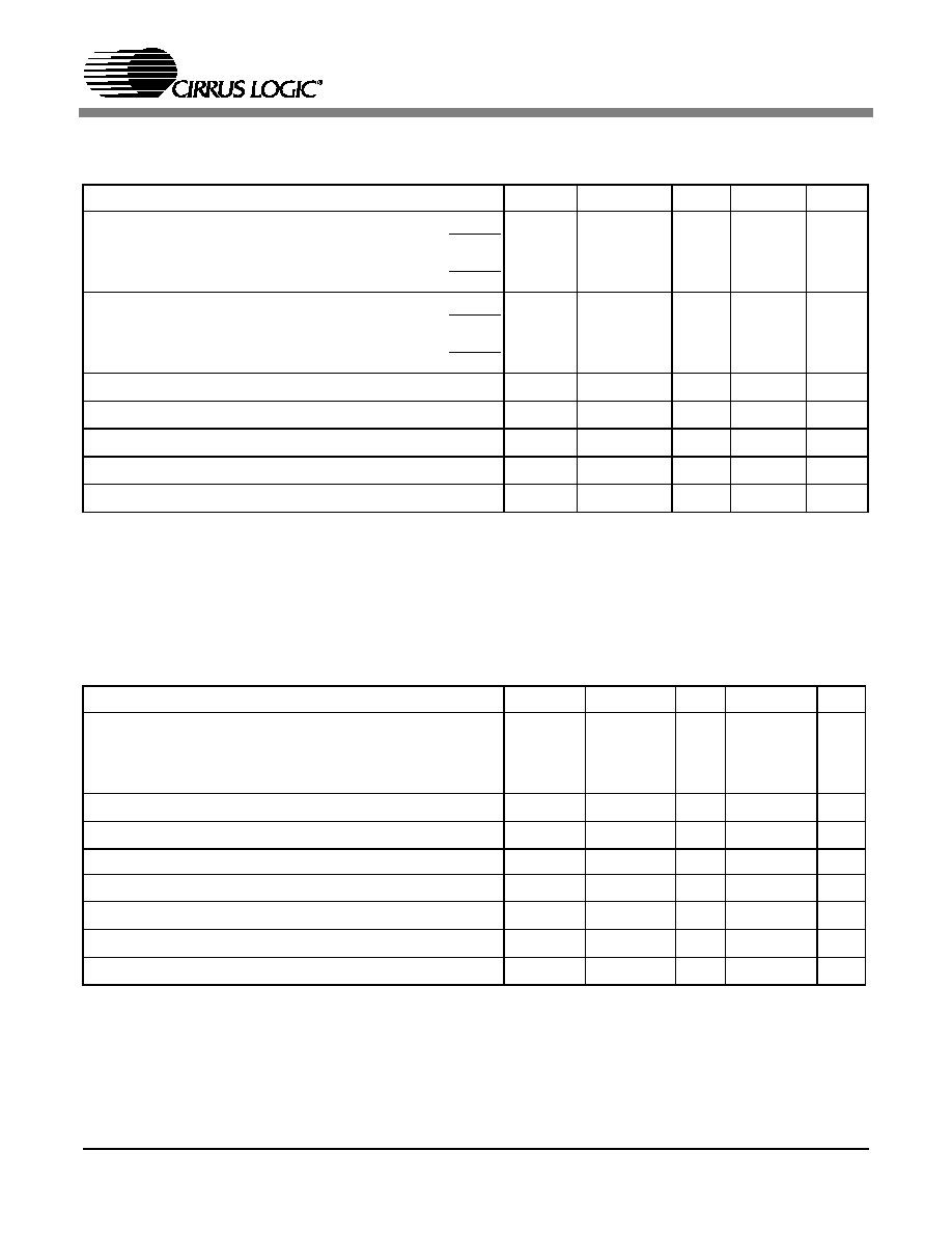
VREFOUT REFERENCE OUTPUT VOLTAGE
Notes: 12. The voltage at VREFOUT is measured across the temperature range. From these measurements the
following formula is used to calculate the VREFOUT Temperature Coefficient:.
5V DIGITAL CHARACTERISTICS
(T
A
= -40 ∞C to +85 ∞C; VA+ = VD+ = 5 V ±10% VA-, DGND = 0 V) (See Notes 3, 4, and 13)
13. Note that the 5 V characteristics are guaranteed by characterization. Only the more rigorous 3.3 V
digital characteristics are actually verified during production test.
14. Applies to all INPUT pins except XIN pin (leakage current < 50 µA) and MODE pin (leakage current <
25 µA).
Parameter
Symbol Min
Typ
Max
Unit
Reference Output
Output Voltage
REFOUT
+2.4
-
+2.6
V
VREFOUT Temperature Coefficient
(Note 12) T
VREFOUT
-
30
60
ppm/∞C
Load Regulation
(Output Current 1 µA Source or Sink)
V
R
-
6
10
mV
Reference Input
Input Voltage Range
VREFIN
+2.4
+2.5
+2.6
V
Input Capacitance
-
4
-
pF
Input CVF Current
-
25
-
nA
Parameter
Symbol Min Typ
Max
Unit
High-Level Input Voltage
All Pins Except XIN, SCLK and RESET
XIN
SCLK and RESET
V
IH
0.6 VD+
(VD+) - 0.5
0.8
VD+
-
-
-
-
-
-
V
V
V
Low-Level Input Voltage
All Pins Except XIN, SCLK, and RESET
XIN
SCLK and RESET
V
IL
-
-
-
-
-
-
0.8
1.5
0.2
VD+
V
V
V
High-Level Output Voltage (except XOUT)
I
out
= +5 mA
V
OH
(VD+) - 1.0
-
-
V
Low-Level Output Voltage (except XOUT)
I
out
= -5 mA
V
OL
-
-
0.4
V
Input Leakage Current
(Note 14)
I
in
-
±1
±10
µA
High Impedance State Leakage Current
I
OZ
-
-
±10
µA
Digital Output Pin Capacitance
C
out
-
5
-
pF
(VREFOUT
MAX
-
VREFOUT
MIN
)
VREFOUT
AVG
T
A
MAX
-
T
A
MIN
1
(
(
)
)
1.0 x 10
(
)
6
T
VREFOUT
=
CS5460A
8
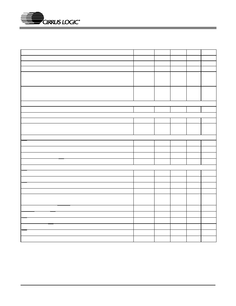
3.3 V DIGITAL CHARACTERISTICS
(T
A
= -40 ∞C to +85 ∞C; VA+ = 5 V ±10%, VD+ = 3.3 V ±10%; VA-, DGND = 0 V) (See Notes 3, 4, and 13)
Notes: 15. All measurements performed under static conditions.
16. If VD+ = 3 V and if XIN input is generated using crystal, then XIN frequency must remain between
2.5 MHz - 5.0 MHz. If using oscillator, full XIN frequency range is available, see
SWITCHING
CHARACTERISTICS
.
ABSOLUTE MAXIMUM RATINGS
(DGND = 0 V; See Note 17) WARNING: Operation at or beyond these limits may result in permanent damage to
the device. Normal operation is not guaranteed at these extremes.
Notes: 17. All voltages with respect to ground.
18. VA+ and VA- must satisfy {(VA+) - (VA-)}
+6.0 V.
19. VD+ and VA- must satisfy {(VD+) - (VA-)}
+6.0 V.
20. Applies to all pins including continuous over-voltage conditions at the analog input (AIN) pins.
21. Transient current of up to 100 mA will not cause SCR latch-up.
22. Maximum DC input current for a power supply pin is ±50 mA.
23. Total power dissipation, including all input currents and output currents.
Parameter
Symbol Min Typ
Max
Unit
High-Level Input Voltage
All Pins Except XIN, XOUT, SCLK, and RESET
XIN
SCLK and RESET
V
IH
0.6 VD+
(VD+) - 0.5
0.8
VD+
-
-
-
-
-
-
V
V
V
Low-Level Input Voltage
All Pins Except XIN, XOUT, SCLK, and RESET
XIN
SCLK and RESET
V
IL
-
-
-
-
-
-
0.48
0.3
0.2
VD+
V
V
V
High-Level Output Voltage (except XIN, XOUT) I
out
= +5 mA
V
OH
(VD+) - 1.0
-
-
V
Low-Level Output Voltage (except XIN, XOUT) I
out
= -5 mA
V
OL
-
-
0.4
V
Input Leakage Current
(Note 14)
I
in
-
±1
±10
µA
3-State Leakage Current
I
OZ
-
-
±10
µA
Digital Output Pin Capacitance
C
out
-
5
-
pF
Parameter
Symbol Min Typ
Max
Unit
DC Power Supplies
(Notes 18 and 19)
Positive Digital
Positive Analog
Negative Analog
VD+
VA+
VA-
-0.3
-0.3
+0.3
-
-
-
+6.0
+6.0
-6.0
V
V
V
Input Current, Any Pin Except Supplies(Note 20, 21, and 22)
I
IN
-
-
±10
mA
Output Current
I
OUT
-
-
±25
mA
Power Dissipation
(Note 23)
P
D
-
-
500
mW
Analog Input Voltage
All Analog Pins
V
INA
(VA-) - 0.3
-
(VA+) + 0.3
V
Digital Input Voltage
All Digital Pins
V
IND
DGND - 0.3
-
(VD+) + 0.3
V
Ambient Operating Temperature
T
A
-40
-
85
∞C
Storage Temperature
T
stg
-65
-
150
∞C
CS5460A
9
SWITCHING CHARACTERISTICS
(T
A
= -40 ∞C to +85 ∞C; VA+ = 5.0 V ±10%; VD+ = 3.0 V ±10% or 5.0 V ±10%; VA- = 0.0 V; Logic Levels:
Logic 0 = 0.0 V, Logic 1 = VD+; CL = 50 pF))
Notes: 24. Device parameters are specified with a 4.096 MHz clock, yet, clocks between 3 MHz to 20 MHz can be
used. However, for input frequencies over 5 MHz, an external oscillator must be used.
25. If external MCLK is used, then duty cycle must be between 45% and 55% to maintain this specification.
26. Specified using 10% and 90% points on wave-form of interest. Output loaded with 50 pF.
27. Oscillator start-up time varies with crystal parameters. This specification does not apply when using an
external clock source.
Parameter
Symbol Min Typ
Max
Unit
Master Clock FrequencyCrystal/Internal Gate Oscillator (Note 24)
MCLK
2.5
4.096
20
MHz
Master Clock Duty Cycle
40
-
60
%
CPUCLK Duty Cycle
(Note 25)
40
60
%
Rise Times
Any Digital Input Except SCLK (Note 26)
SCLK
Any Digital Output
t
rise
-
-
-
-
-
50
1.0
100
-
µs
µs
ns
Fall Times
Any Digital Input Except SCLK (Note 26)
SCLK
Any Digital Output
t
fall
-
-
-
-
-
50
1.0
100
-
µs
µs
ns
Start-up
Oscillator Start-Up Time
XTAL = 4.096 MHz (Note 27)
t
ost
-
60
-
ms
Serial Port Timing
Serial Clock Frequency
SCLK
-
-
2
MHz
Serial Clock
Pulse Width High
Pulse Width Low
t
1
t
2
200
200
-
-
-
-
ns
ns
SDI Timing
CS Falling to SCLK Rising
t
3
50
-
-
ns
Data Set-up Time Prior to SCLK Rising
t
4
50
-
-
ns
Data Hold Time After SCLK Rising
t
5
100
-
-
ns
SCLK Falling Prior to CS Disable
t
6
100
-
-
ns
SDO Timing
CS Falling to SDI Driving
t
7
-
20
50
ns
SCLK Falling to New Data Bit
t
8
-
20
50
ns
CS Rising to SDO Hi-Z
t
9
-
20
50
ns
Auto-Boot Timing
Serial Clock
Pulse Width High
Pulse Width Low
t
10
t
11
8
8
MCLK
MCLK
MODE setup time to RESET Rising
t
12
50
ns
RESET rising to CS falling
t
13
48
MCLK
CS falling to SCLK rising
t
14
100
8
MCLK
SCLK falling to CS rising
t
15
16
MCLK
CS rising to driving MODE low (to end auto-boot sequence).
t
16
50
ns
SDO guaranteed setup time to SCLK rising
t
17
100
ns

CS5460A
10
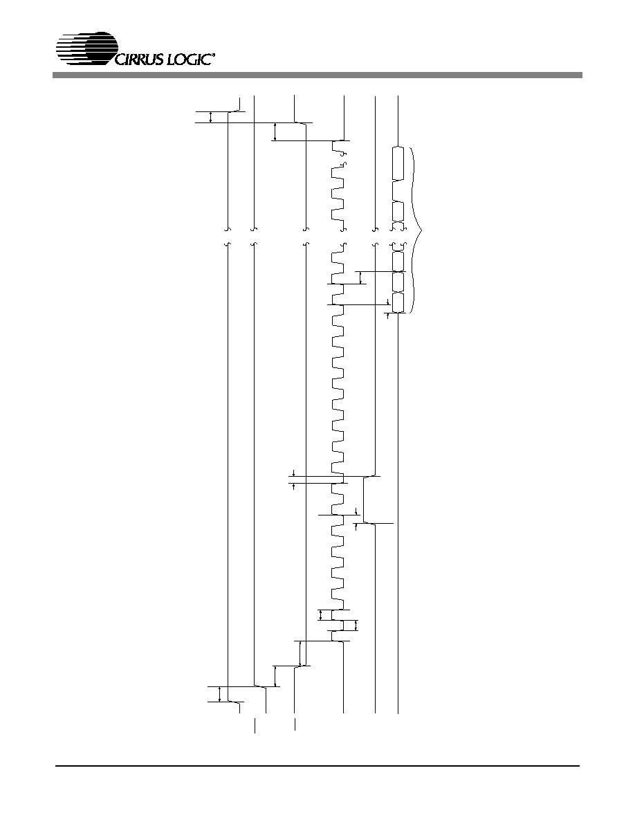
CS
SC
L
K
MS
B
M
S
B
-
1
LS
B
t 2
t 1
t 3
SD
I
MS
B
M
S
B
-
1
LS
B
C
o
m
m
an
d T
i
m
e
8 S
C
LK
s
LS
B
t 6
MS
B
M
S
B
-
1
LS
B
MS
B
M
S
B
-
1
H
i
g
h
By
t
e
M
i
d
By
t
e
L
o
w
By
t
e
t
t
45
S
D
I
W
r
i
t
e
T
i
m
i
n
g
(No
t
to
S
cal
e)
CS
SD
O
SC
LK
MS
B
M
S
B
-
1
LS
B
t 2
t 1
t 8
t 7
SD
I
MS
B
M
S
B
-
1
LS
B
C
o
m
m
an
d Ti
m
e
8 S
C
L
K
s
LS
B
t 9
MS
B
M
S
B
-
1
LS
B
MS
B
M
S
B
-
1
H
i
gh B
y
t
e
M
i
d By
t
e
Lo
w
By
t
e
M
u
s
t
s
t
r
o
b
e
"
S
Y
N
C
0
"
c
o
m
m
a
n
d
o
n
S
D
I
w
h
e
n
r
e
a
d
i
n
g
e
a
c
h
b
y
t
e
o
f
d
a
t
a
f
r
o
m
S
D
O
.
S
D
O
R
e
a
d
Ti
m
i
n
g
(
N
ot
t
o
S
c
a
l
e
)
Figure 1. CS5460A Read and Write Timing Diagrams
CS5460A
11
RE
S
SD
I
SC
L
K
t
8
t
14
t
13
t
1
1
t
10
SD
O
CS
t
5
t
4
D
a
t
a
f
r
o
m
EEPR
O
M
(
O
ut
put
)
(
O
ut
put
)
(
O
ut
put
)
(
I
nput
)
MO
D
E
(
I
nput
)
t
12
t
15
t
16
ST
O
P
BI
T
L
AST
8
BI
T
S
(
I
nput
)
t
17
Fi
gur
e 2
.
CS5
460A
Aut
o
-
B
oot
Seq
u
ence
Ti
m
i
ng

CS5460A
12
2. GENERAL DESCRIPTION
The CS5460A is a CMOS monolithic power mea-
surement device with a real power/energy compu-
tation engine. The CS5460A combines two
programmable gain amplifiers, two
modulators,
two high rate filters, system calibration, and
rms/power calculation functions to provide instan-
taneous voltage/current/power data samples as
well as periodic computation results for real (bill-
able) energy, V
RMS
, and I
RMS
. In order to accom-
modate lower cost metering applications, the
CS5460A can also generate pulse-train signals on
certain output pins, for which the number of pulses
emitted on the pins is proportional to the quantity of
real (billable) energy registered by the device.
The CS5460A is optimized for power measure-
ment applications and is designed to interface to a
shunt or current transformer to measure current,
and to a resistive divider or potential transformer to
measure voltage. To accommodate various input
voltage levels, the current channel includes a pro-
grammable gain amplifier (PGA) which provides
two full-scale input levels, while the voltage chan-
nel's PGA provides a single input voltage range.
With a single +5 V supply on VA+/-, both of the
CS5460A's input channels can accomodate com-
mon mode + signal levels between -0.25 V and
VA+.
The CS5460A includes two high-rate digital filters
(one per channel), which decimate/integrate the
output from the 2
modulators. The filters yield
24-bit output data at a (MCLK/K)/1024 output word
rate (OWR). The OWR can be thought of as the ef-
fective sample frequency of the voltage channel and
the current channel.
To facilitate communication to a microcontroller,
the CS5460A includes a simple three-wire serial
interface which is SPITM and MicrowireTM compati-
ble. The serial port has a Schmitt Trigger input on
its SCLK (serial clock) and RESET pins to allow for
slow rise time signals.
2.1 Theory of Operation
A computational flow diagram for the two data
paths is shown in Fig. 3. The reader should refer to
this diagram while reading the following data pro-
cessing description, which is covered
block-by-block.
2.1.1
Modulators
The analog waveforms at the voltage/current chan-
nel inputs are subject to the gains of the input
PGAs (not shown in Figure 3). These waveforms
are then sampled by the delta-sigma modulators at
a rate of (MCLK/K)/8 Sps.
2.1.2 High-Rate Digital Low-Pass Filters
The data is then low-pass filtered, to remove
high-frequency noise from the modulator output.
Referring to Figure 3, the high rate filter on the volt-
age channel is implemented as a fixed Sinc
2
filter.
The current channel uses a Sinc
4
filter, which al-
lows the current channel to make accurate mea-
surements over a wider span of the total input
range, in comparison to the accuracy range of the
voltage channel. (This subject is discussed more in
Section 2.2.1)
Also note from Figure 3 that the digital data on the
voltage channel is subjected to a variable time-de-
lay filter. The amount of delay depends on the val-
ue of the seven phase compensation bits (see
Phase Compensation). Note that when the phase
compensation bits PC[6:0] are set to their default
setting of "0000000" (and if MCLK/K = 4.096 MHz)
then the nominal time delay that is imposed on the
original analog voltage input signal, with respect to
the original analog current input signal, is ~1.0
µ
s.
This translates into a delay of ~0.0216 degrees at
60 Hz.
2.1.3 Digital Compensation Filters
The data from both channels is then passed
through two FIR compensation filters, whose pur-
pose is to compensate for the magnitude roll-off of
the low-pass filtering operation (mentioned earli-
er).
2.1.4 Digital High-Pass Filters
Both channels provide an optional high-pass filter
(denoted as "HPF" in Figure 3) which can be en-
gaged into the signal path, to remove the DC con-
tent from the current/voltage signal before the
RMS/energy calculations are made. These filters
are activated by enabling certain bits in the Config-
uration Register.
If e high-pass filter is engaged in only one of the
two channels, then the all-pass filter (see "APF" in

CS5460A
13
Figure 3) will be enabled on the other channel; in
order to preserve the relative phase relationship
between the voltage-sense and current-sense in-
put signals. For example, if the HPF is engaged for
the voltage channel, but not the current channel,
then the APF will be engaged in the current channel,
to nullify the additional phase delay introduced by
the high-pass filter in the current channel.
2.1.5 Overall Filter Response
When the CS5460A is driven with a 4.096 MHz
clock (K = 1), the composite magnitude response
(over frequency) of the voltage channel's input fil-
ter network is shown in Figure 4, while the com-
posite magnitude response of the current
channel's input filter network is given in Figure 5.
Note that the composite filter response of both
channels scales with MCLK frequency and K.
2.1.6 Gain and DC Offset Adjustment
After filtering, the instantaneous voltage and cur-
rent digital codes are subjected to offset/gain ad-
justments, based on the values in the DC offset
registers (additive) and the gain registers (multipli-
cative). These registers are used for calibration of
the device (see
Section 3.8, Calibration). After off-
set and gain, the 24-bit instantaneous data sample
values are stored in the Instantaneous Voltage and
Current Registers.
2.1.7 Real Energy and RMS Computations
The digital instantaneous voltage and current data
is then processed further. Referring to Figure 3, the
instantaneous voltage/current data samples are
multiplied together (one multiplication for each pair
of voltage/current samples) to form instantaneous
(real) power samples. After each A/D conversion
cycle, the new instantaneous power sample is
stored in the Instantaneous Power Register.
The instantaneous power samples are then
grouped into sets of N samples (where N = value in
Cycle Count Register). The cumulative sum of
each successive set of N instantaneous power is
used to compute the result stored in the Energy
Register, which will be proportional to the amount
of real energy registered by the device during the
most recent N A/D conversion cycles. Note from
Figure 3 that the bits in this running energy sum
are right-shifted 12 times (divided by 4096) to
avoid overflow in the Energy Register. RMS calcu-
lations are also performed on the data using the
last N instantaneous voltage/current samples, and
these results can be read from the RMS Voltage
Register and the RMS Current Register.
2.2 Performing Measurements
To summarize Section 2.1, the CS5460A performs
measurements of instantaneous current and in-
stantaneous voltage, and from this, performs com-
putations of the corresponding instantaneous
power, as well as periodic calculations of real en-
ergy, RMS current, and RMS voltage. These mea-
surement/calculation results are available in the
form of 24-bit signed and unsigned words. The
scaling of all output words is normalized to unity
VOLTAGE
SINC2
+
x
V
*
gn
x
V *
CURRENT
SINC4
+
x
I
*
gn
x
x
TBC *
DELAY
REG
DELAY
REG
FIR
HPF
APF
Configuration Register *
PC[6:0] Bits
x
I
*
RMS
N
V
*
RMS
N
˜ 4096
E to F
E *
E
E
out
dir
PULSE-RATE*
* DENOTES REGISTER NAME
HPF
APF
FIR
SINC2
I *
P*
N
SINC2
-
-
I
ACoff
*
I
DCoff
*
V
ACoff
*
V
DCoff
*
+
P
off
*
˜
N
˜
N
Figure 3. Data Flow.

CS5460A
14
full-scale. Note that the 24-bit
signed output words
are expressed in two's complement format. The
24-bit data words in the CS5460A output registers
represent values between 0 and 1 (for unsigned
output registers) or between -1 and +1 (for signed
output registers). A register value of 1 represents
the maximum possible value. Note that a value of
1.0 is never actually obtained in the registers of the
CS5460A. As an illustration, in any of the signed
output registers, the maximum register value is
[(2^23 - 1) / (2^23)] = 0.999999880791. After each
A/D conversion, the CRDY bit will be asserted in
the Status Register, and the INT pin will also be-
come active if the CRDY bit is unmasked (in the
Mask Register). The assertion of the CRDY bit in-
dicates that new instantaneous 24-bit voltage and
current samples have been collected, and these
two samples have also been multiplied together to
provide a corresponding instantaneous 24-bit pow-
er sample.
Table 1 conveys the typical relationship between
the differential input voltage (across the "+" and "-"
input pins of the voltage channel input) and the cor-
responding output code in the Instantaneous Volt-
age Register. Note that this table is applicable for
the current channel if the current channel's PGA
gain is set for the "10x" gain mode.
The V
RMS
, I
RMS
, and energy calculations are up-
dated every N conversions (which is known as 1
"
computation cycle"), where N is the value in the
Cycle Count Register. At the end of each computa-
tion cycle, the DRDY bit in the Mask Register will
be set, and the INT pin will become active if the
DRDY bit is unmasked.
DRDY is set only after each computation cycle has
completed, whereas the CRDY bit is asserted after
each individual A/D conversion. Bits asserted by
the CS5460A must be cleared before being assert-
ed again. If the Cycle Count Register value (N) is
set to 1, all output calculations are instantaneous,
and DRDY will indicate when instantaneous calcu-
lations are finished, just like the CRDY bit. For the
RMS results to be valid, the Cycle-Count Register
must be set to a value greater than 10.
The computation cycle frequency is derived from
the master clock, and has a value of
(MCLK/K)/(1024*N). Under default conditions, with
-2.5
-2.0
-1.5
-1.0
-0.5
0.0
0.5
Frequency (Hertz)
G
a
in
(
d
B
)
0
200
400
600
800
1000 1200 1400
1600 1800 2000
Figure 4. Voltage Input Filter Characteristics
Input Voltage (DC)
Output Code
(hexidecimal)
Output Code
(decimal)
+250 mV
7FFFFF
8388607
14.9 nV to 44.7 nV
000001
1
-14.9 nV to 14.9 nV
000000
0
-44.7 nV to -14.9 nV
FFFFFF
-1
-250 mV
800000
-8388608
Table 1. Differential Input Voltage vs. Output Code
-2.5
-2
-1.5
-1
-0.5
0
0.5
0
200
400
600
800
1000 1200
1400 1600
1800 2000
Ga
i
n
(
d
B
)
Frequency (Hertz)
Figure 5. Current Input Filter Characteristics

CS5460A
15
a 4.096 MHz clock at XIN, and K = 1, instanta-
neous A/D conversions for voltage, current, and
power are performed at a 4000 Sps rate, whereas
I
RMS
, V
RMS
, and energy calculations are per-
formed at a 1 Sps rate.
2.2.1 CS5460A Linearity Performance
Table 2 lists the range of input levels (as a percent-
age of full-scale) over which the (linearity + varia-
tion) of the results in the Vrms, Irms and Energy
Registers are guaranteed to be within
±
0.1 % of
reading after the completion of each successive
computation cycle. Note that until the CS5460A is
calibrated (see Calibration) the
accuracy of the
CS5460A with respect to a reference line-voltage
and line-current level on the power mains is not
guaranteed to within
±
0.1%. After both channels of
the device are calibrated for offset/gain, the ±0.1%
of reading spec will also reflect accuracy of the
Vrms, Irms, and Energy Register results. Finally,
observe that the maximum (full-scale) differential
input voltage for the voltage channel (and current
channel, when its PGA is set for 10x gain) is
250 mV (nominal). If the gain registers of both
channels are set to 1 (default) and the two DC
offset registers are set to zero (default), then a
250mV DC signal applied to the voltage/current
inputs will measure at (or near) the maximum
value of 0.9999... in the RMS Current/Voltage
Registers. Remember that the RMS value of a
250 mV (DC) signal is also 250 mV. However, for
either input channel, it would not be practical to in-
ject a sinusoidal voltage with RMS value of
250 mV. This is because when the instantaneous
value of such a sine wave is at or near the level of
its positive/negative peak regions (over each cy-
cle), the voltage level of this signal would exceed
the maximum differential input voltage range of the
input channels. The largest sine wave voltage sig-
nal that can be presented across the inputs, with
no saturation of the inputs, is:
250 mV / sqrt(2) = ~176.78 mV (RMS),
which is ~70.7% of full-scale. This would imply that
for the current channel, the (linearity+variation) tol-
erance of the RMS measurements for a purely si-
nusoidal 60 Hz input signal could be measured to
within
±
0.1% of reading over a magnitude range of
0.2% - 70.7% of the maximum full-scale differen-
tial input voltage level.
The range over which the (linearity + variation) will
remain within ±0.1% can often be increased by se-
lecting a value for the Cycle-Count Register such
that the time duration of one computation cycle is
equal to (or very close to) a
whole-number of pow-
er-line cycles (and N must be greater than or equal
to 4000). For example, with the cycle count set to
4200, the ±0.1% of reading (linearity + variation)
range for measurement of a 60 Hz sinusoidal cur-
rent-sense voltage signal can be increased beyond
the range of 0.2% - 70.7%. The accuracy range
will be increased because (4200 samples / 60 Hz)
is a whole number of cycles (70). Note that this in-
crease in the measurement range refers to an ex-
tension of the
low end of the input scale (i.e., this
does
not extend the high-end of the range above
100% of full-scale). This enables accurate mea-
surement of even smaller power-line current lev-
els, thereby extending the load range over which
the power meter can make accurate energy mea-
surements. Increasing the accuracy range can be
beneficial for power metering applications which
require accurate power metering over a very large
load range.
2.2.2 Single Computation Cycle (C=0)
Note that `C' refers to the value of the C bit, con-
tained in the `Start Conversions' command (see
Section 4.1). This commands instructs the
CS5460A to perform conversions in `single compu-
tation cycle' data acquisition mode. Based on the
value in the Cycle Count Register, a single compu-
tation cycle is performed after a `Start Conversions'
command is sent to the serial interface. After the
computations are complete, DRDY is set. 32
SCLKs are then needed to read out a calculation
Energy
Vrms
Irms
Range (% of FS)
0.1% - 100%
50% - 100%
0.2% - 100%
Max. Differential
Input
not applicable
V-channel:
±250 mV
I-channel:
±250
mV 10x
±50
mV 50x
Linearity
0.1% of
reading
0.1% of
reading
0.1% of
reading
Table 2. Available range of ±0.1% output linearity, with
default settings in the gain/offset registers.

CS5460A
16
result from one of several result registers. The first
8 SCLKs are used to clock in the command to de-
termine which register is to be read. The last 24
SCLKs are used to read the desired register. After
reading the data, the serial port remains in the
ac-
tive state, and waits for a new command to be is-
sued. (See Section 3 for more details on reading
register data from the CS5460A).
2.2.3 Continuous Computation Cycles
(C=1)
When C = 1, the CS5460A will perform conversions
in `continuous computation cycles' data acquisition
mode. Based on the information provided in the Cy-
cle Count Register, computation cycles are repeat-
edly performed on the voltage and current channels
(after every N conversions). Computation cycles
cannot be started/stopped on a `per-channel' basis.
After each computation cycle is completed, DRDY
is set. Thirty-two SCLKs are then needed to read a
register. The first 8 SCLKs are used to clock in the
command to determine which results register is to
be read. The last 24 SCLKs are used to read out the
24-bit calculation result. While in this acquisition
mode, the designer/programmer may choose to ac-
quire (read) only those calculations required for
their particular application, as DRDY repeatedly in-
dicates the availability of new data. Note again that
the MCU firmware must reset the DRDY bit to "0"
before it can be asserted again.
Referring again to Figure 3, note that within the
Irms and Vrms data paths, prior to the square-root
operation, the instantaneous voltage/current data
is low-pass filtered by a Sinc
2
filter. Then the data
is decimated to every Nth sample. Because of the
Sinc
2
filter operation, the first output for each chan-
nel will be invalid (i.e. all RMS calculations are in-
valid in the `single computation cycle' data
acquisition mode and the first RMS calculation re-
sults will be invalid in the `continuous computation
cycles' data acquisition mode). However, all ener-
gy calculations will be valid since energy calcula-
tions do not require this Sinc
2
operation.
If the 'Start Conversions' command is issued to the
CS5460A (see
Section 4.1, Commands (Write
Only)), and if the `C' bit in this command is set to a
value of `1', the device will remain in its
active state.
Once commanded into
continuous computation
cycles data acquisition mode, the CS5460A will
continue to perform A/D conversions on the volt-
age/current channels, as well as all subsequent
calculations, until:
1) the `Power-Up/Halt' command is received
through the serial interface, or
2) loss of power, or
3) the RS bit in the Configuration Register is as-
serted (`software reset'), or
4) the /RESET pin is asserted and then de-assert-
ed (`hardware reset').
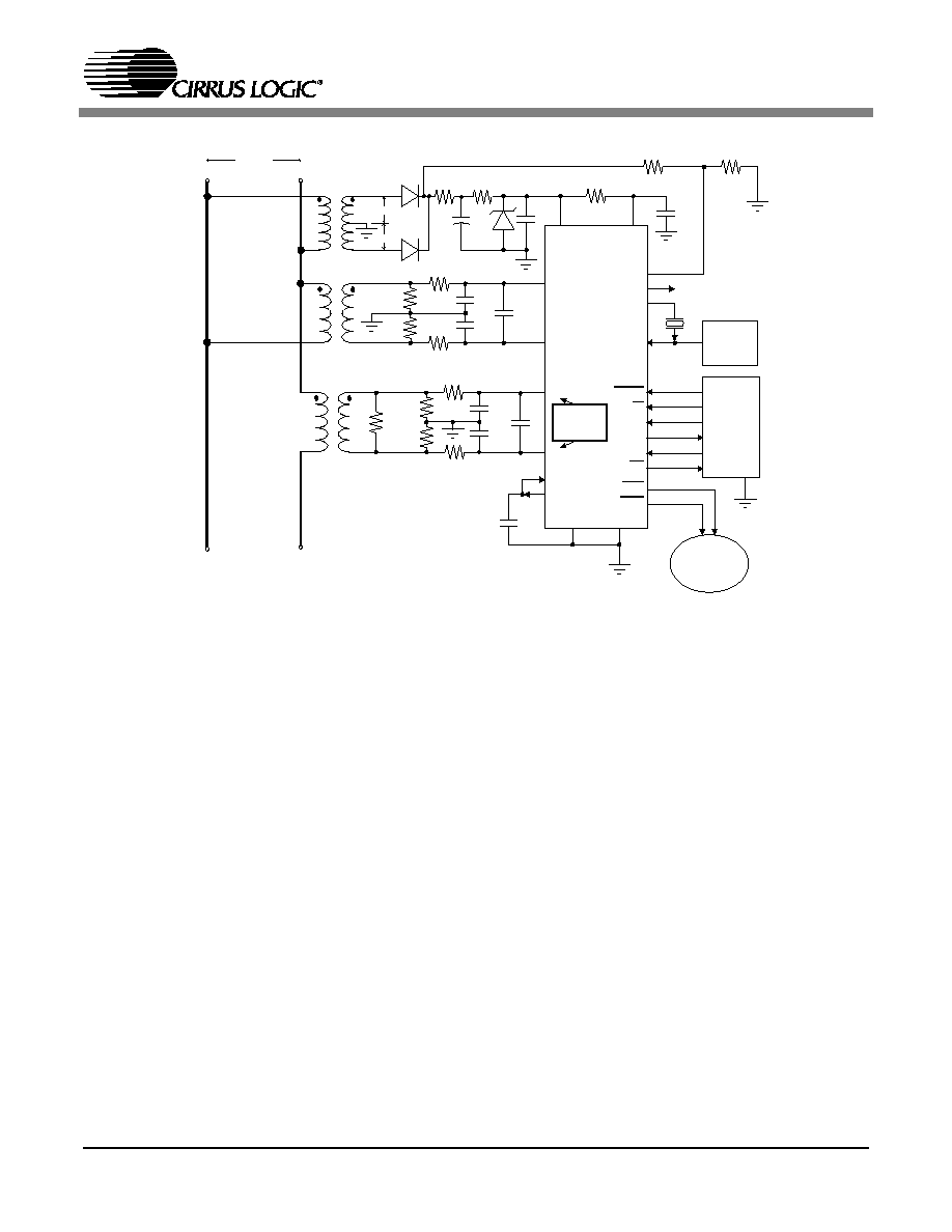
2.3 Basic Application Circuit
Configurations
Figure 6 shows the CS5460A connected to a ser-
vice to measure power in a single-phase 2-wire
system operating from a single power supply. Note
that in this diagram the shunt resistor used to mon-
itor the line current is connected on the "Line" (hot)
side of the power mains. In most residential power
metering applications, the power meter's cur-
rent-sense shunt resistor is intentionally placed on
the `hot' side of the power mains in order to help
detect any attempt by the subscriber to steal pow-
er. In this type of shunt-resistor configuration, note
that the common-mode level of the CS5460A must
be referenced to the hot side of the power line. This
means that the common-mode potential of the
CS5460A will typically oscillate to very high posi-
tive voltage levels, as well as very high negative
voltage levels, with respect to earth ground poten-
tial.
The designer must therefore be careful when
attempting to interface the CS5460A's digital out-
put lines to an external digital interface (such as a
LAN connection or other communication network).
Such digital communication networks may require
that the CMOS-level digital interface to the meter is
referenced to an earth-ground. In such cases, the
CS5460A's digital serial interface pins
must be iso-
lated from the external digital interface, so that
there is no conflict between the ground references
of the meter and the external interface. The
CS5460A and associate circuitry should be en-
closed in a protective insulated case when used in
this configuration, to avoid risk of harmful electric
shock to humans/animals/etc.
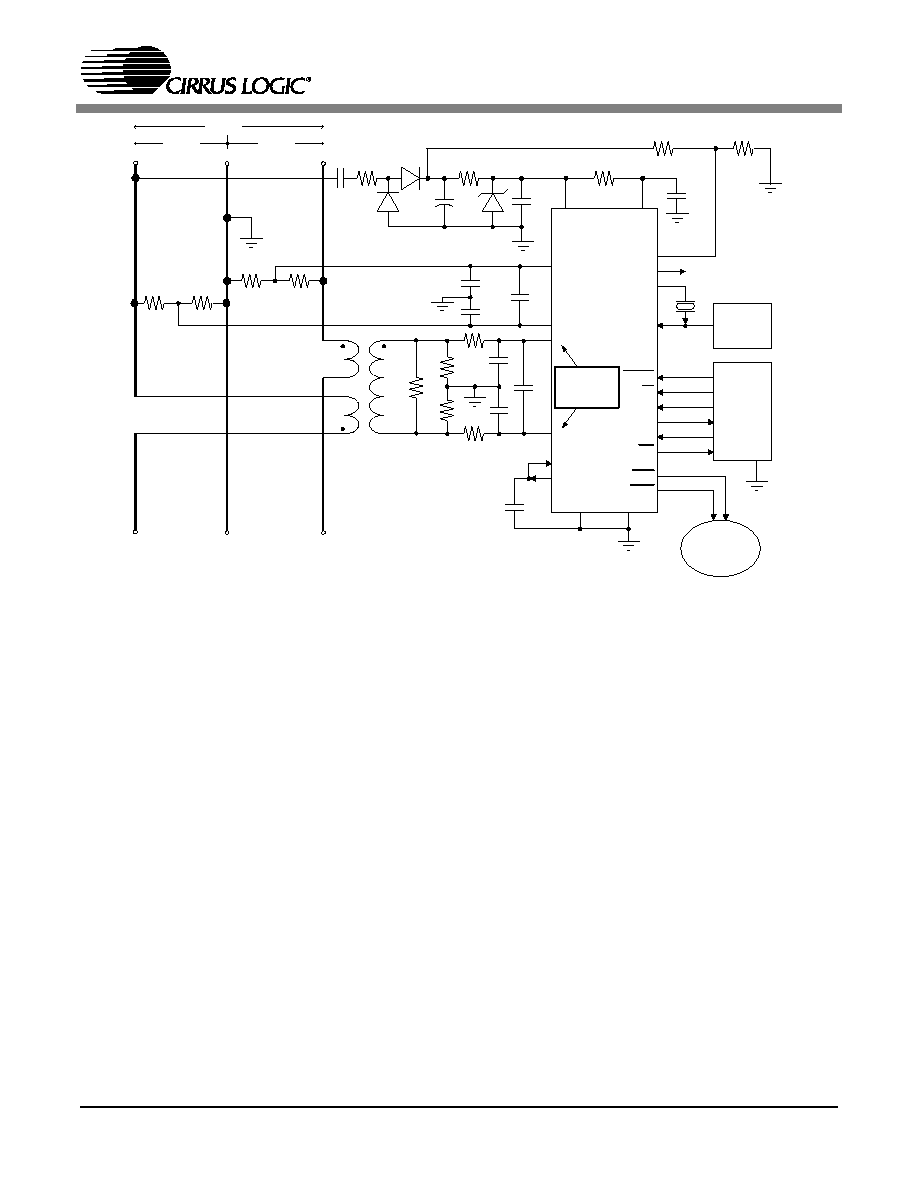
Figure 7 shows how the same single-phase
two-wire system can be metered while achieving

CS5460A
17
complete isolation from the power lines. This isola-
tion is achieved using three transformers. One
transformer is a general-purpose voltage trans-
former, used to supply the on-board DC power to
the CS5460A. A second transformer is a high-pre-
cision, low-impedance voltage transformer (often
called a `potential transformer') with very little
roll-off/phase delay, even at the higher harmonics.
A current transformer is then used to sense the line
current. A burden resistor placed across the sec-
ondary of the current transformer creates the cur-
rent-sense voltage signal, for the CS5460A's
current channel inputs. Because the CS5460A is
not directly connected to the power mains, isola-
tion is not required for the CS5460A's digital inter-
face.
Figure 8 shows the CS5460A configured to mea-
sure power in a single-phase 3-wire system. In
many 3-wire residential power systems within the
United States, only the two Line terminals are
available (neutral is not available). Figure 9 shows
how the CS5460A can be configured to meter a
3-wire system when no neutral is available.
VA+
VD+
0.1 µF
100 µF
500
470 nF
500
N
R
1
R
2
10
14
VIN+
9
VIN-
IIN-
10
15
16
IIN+
PFMON
CPUCLK
XOUT
XIN
Optional
Clock
Source
Serial
Data
Interface
RESET
17
2
1
24
19
CS
7
SDI
23
SDO
6
SCLK
5
INT
20
EDIR
EOUT
0.1 µF
VREFIN
12
VREFOUT
11
VA-
DGND
13
4
3
To Service
2.5 MHz to
20 MHz
0.1 µF
C
10 k
5 k
L
R
Shunt
V+
*
* Refer to Input Protection
CS5460A
*
** Refer to Input Filtering
R
V-
*
R
I-
*
R
I+
*
C
I+
* *
IS
O
L
A
T
IO
N
120 VAC
Mech. Counter
Stepper Motor
or
22
21
+
NOTE: Current channel
input measures voltage
(just like voltage input).
C
V-
* *
C
I-
* *
C* *
Vdiff
C* *
Idiff
Figure 6. Typical Connection Diagram (One-Phase 2-Wire, Direct Connect to Power Line)
CS5460A
18
VA+
VD+
0.1µF
200µF
200
N
10
14
VIN+
9
VIN-
IIN-
10
15
16
IIN+
PFMON
CPUCLK
XOUT
XIN
Optional
Clock
Source
RESET
17
2
1
24
CS
SDI
SDO
SCLK
INT
EDIR
22
EOUT
21
0.1 µF
VREFIN
12
VREFOUT
11
VA-
DGND
13
4
3
To Service
2.5 MHz to
20 MHz
0.1 µF
10 k
5 k
L
* Refer to Input Protection
M:1
R
N:1
Low Phase-Shift
Potential Transformer
Current
Transformer
CS5460A
** Refer to Input Filtering
R
V+
*
R
V-
*
C
Vdiff
* *
R
I-
*
R
I+
*
C* *
Burden
Idiff
Voltage
Transformer
120 VAC
12 VAC
12 VAC
200
Serial
Data
Interface
19
7
23
6
5
20
Mech. Counter
Stepper Motor
or
1k
1k
1k
1k
+
NOTE: Current channel
input measures voltage
(just like voltage input).
C
V+
* *
C
V-
* *
C
I+
* *
C
I-
* *
Figure 7. Typical Connection Diagram (One-Phase 2-Wire, Isolated from Power Line)
CS5460A
19
VA+
VD+
0.1 µF
100 µF
500
470 nF
500
N
R
3
R
4
R
Burden
10
14
VIN+
9
VIN-
IIN-
10
16
15
IIN+
PFMON
CPUCLK
XOUT
XIN
Optional
Clock
Source
RESET
17
2
1
24
CS
SD
SDO
SCLK
INT
EDIR
EOUT
0.1 µF
VREFIN
12
VREFOUT
11
DGND
13
4
3
To Service
2.5 MHz to
20 MHz
0.1 µF
L
1
L
2
10 k
5 k
VA-
* Refer to Input Protection
R
1
R
2
To Service
** Refer to Input Filtering
R
I+
*
R
I-
*
22
21
Mech. Counter
Stepper Motor
or
1k
1k
120 VAC
120 VAC
240 VAC
Serial
Data
Interface
19
7
23
6
5
20
I
Earth
Ground
C* *
Idiff
C* *
Vdiff
+
NOTE: Current channel
input measures voltage
(just like voltage input).
C
I+
* *
C* *
I-
C
V+
**
C* *
V-
CS5460A
Figure 8. Typical Connection Diagram (One-Phase 3-Wire)

CS5460A
20
VA+
VD+
CS5460A
0.1 µF
1
k
235 nF
500
R
1
R
2
10
14
VIN+
9
VIN-
IIN-
10
16
15
IIN+
PFMON
CPUCLK
XOUT
XIN
Optional
Clock
Source
RESET
17
2
1
24
CS
SDI
SDO
SCLK
INT
EDIR
EOUT
0.1 µF
VREFIN
12
VREFOUT
11
DGND
13
4
3
To Service
2.5 MHz to
20 MHz
0.1 µF
L
1
L
2
10 k
5 k
VA-
C
V+
* Refer to Input Protection
*
To Service
*
** Refer to Input Filtering
R
I+
*
R
I-
*
R
V-
*
Serial
Data
Interface
19
7
23
6
5
20
IS
O
L
A
T
IO
N
22
21
Mech. Counter
Stepper Motor
or
R
Burden
1k
1k
240 VAC
+
NOTE: Current channel
input measures voltage
(just like voltage input).
C**
V-
C* *
Vdiff
C
I+
**
C* *
I-
C* *
Idiff
100 µF
Figure 9. Typical Connection Diagram (One-Phase 3-Wire - No Neutral Available)

CS5460A
21
3. FUNCTIONAL DESCRIPTION
3.1 Pulse-Rate Output
As an alternative to reading the real energy
through the serial port, the EOUT and EDIR pins
provide a simple interface with which signed ener-
gy can be accumulated. Each EOUT pulse repre-
sents a predetermined quantity of energy. The
quantity of energy represented in one pulse can be
varied by adjusting the value in the Pulse-Rate
Register. Corresponding pulses on the EDIR out-
put pin signify that the sign of the energy is nega-
tive. Note that these pulses are not influenced by
the value of the Cycle-Count Register, and they
have no reliance on the computation cycle, de-
scribed earlier. With MCLK = 4.096 MHz, K = 1,
the pulses will have an average frequency (in Hz)
equal to the frequency setting in the Pulse Rate
Register when the input signals into the voltage
and current channels cause full-scale readings in
the Instantaneous Voltage and Current Registers.
When MCLK/K is not equal to 4.096 MHz, the
pulse-rate should be scaled by a factor of
4.096 MHz / (MCLK/K) to get the actual output
pulse-rate.
EXAMPLE #1: For a power line with maximum rat-
ed levels of 250 V (RMS) and 20 A (RMS), the
pulse-frequency on the EOUT pin needs to be
`IR' = 100 pulses-per-second (100 Hz) when the
RMS-voltage and RMS-current levels on the power
line are 220 V and 15 A respectively. To meet this
requirement, the pulse-rate frequency (`PR') in the
Pulse-Rate Register must be set accordingly.
After calibration, the first step to finding the value
of `PR' is to set the voltage and current sensor gain
constants, K
V
and K
I
, such that there will be ac-
ceptable voltage levels on the CS5460A inputs
when the power line voltage and current levels are
at the maximum values of 250 V and 20 A. K
V
and
K
I
are needed to determine the appropriate ratios
of the voltage/current transformers and/or shunt
resistor values to use in the front-end voltage/cur-
rent sensor networks.
For a sinewave, the largest RMS value that can be
accurately measured (without over-driving the in-
puts) will register ~0.7071 of the maximum DC in-
put level. Since power signals are often not
perfectly sinusoidal in real-world situations, and to
provide for some over-range capability, the RMS
Voltage Register and RMS Current Register is set
to measure 0.6 when the RMS-values of the
line-voltage and line-current levels are 250 V and
20 A. Therefore, when the RMS registers measure
0.6, the voltage level at the inputs will be
0.6 x 250 mV = 150 mV. The sensor gain con-
stants, K
V
and K
I
, are determined by demanding
that the voltage and current channel inputs should
be 150 mV RMS when the power line voltage and
current are at the maximum values of 250 V and
20 A.
K
V
= 150 mV / 250 V = 0.0006
K
I
= 150 mV / 20 A = 0.0075
These sensor gain constants are used to calculate
what the input voltage levels will be on the
CS5460A inputs when the line-voltage and
line-current are 220 V and 15 A. These values are
V
Vnom
and V
Inom.
V
Vnom
= K
V
* 220 V = 132 mV
V
Inom
= K
I
* 15 A = 112.5 mV
The pulse rate on EOUT will be at `PR' pulses per
second (Hz) when the RMS-levels of voltage/cur-
rent inputs are at 250 mV. When the voltage/cur-
rent inputs are set at V
Vnom
and V
Inom
, the pulse
rate needs to be `IR' = 100 pulses per second. IR
will be some percentage of PR. The percentage is
defined by the ratios of V
Vnom
/250 mV and
V
Inom
/250 mV with the following formula:
From this equation the value of `PR' is shown as:.
Therefore the Pulse-Rate Register is set to
~420.875 Hz, or 0x00349C.
The above equation is valid when current channel
is set to x10 gain. If current channel gain is set to
x50, then the equation becomes:
PulseRate
IR
PR
V
Vnom
250mV
-------------------
V
I nom
250mV
-------------------
=
=
PR
IR
V
Vnom
250mV
------------------
V
Inom
250mV
------------------
◊
--------------------------------------------
100Hz
132mV
250mV
------------------
112.5mV
250mV
-----------------------
◊
------------------------------------------------
=
=
PR
IR
V
Vnom
250mV
------------------
V
Inom
50mV
---------------
◊
-----------------------------------------
=

CS5460A
22
EXAMPLE #2: The required number of pulses per
unit energy present at EOUT is specified to be
500 pulses/kW-hr; given that the maximum
line-voltage is 250 V (RMS) and the maximum
line-current is 20 A (RMS). In such a situation, the
nominal line voltage and current do not determine
the appropriate pulse-rate setting. Instead, the
maximum line levels must be considered. As be-
fore, the given maximum line-voltage and line-cur-
rent levels are used to determine K
V
and K
I
:
K
V
= 150 mV / 250 V = 0.0006
K
I
= 150 mV / 20 A = 0.0075
Again the sensor gains are calculated such that the
maximum line-voltage and line-current levels will
measure as 0.6 in the RMS Voltage Register and
RMS Current Register.
The required Pulse-Rate Register setting is now
determined by using the following equation:
Therefore PR = ~1.929 Hz.
Note that the Pulse-Rate Register cannot be set to
a frequency of exactly 1.929 Hz. The closest set-
ting that the Pulse-Rate Register can obtain is
0x00003E = 1.9375 Hz. To improve the accuracy,
either gain register can be programmed to correct
for the round-off error in PR. This value would be
calculated as
In the last example, suppose a value for MCLK/K
of 3.05856 MHz. When MCLK/K is not equal to
4.096 MHz, the result for `PR' that is calculated for
the Pulse-Rate Register must be scaled by a cor-
rection factor of: 4.096 MHz / (MCLK/K). In this
case the result is scaled by 4.096/3.05856 to get a
final PR result of ~2.583 Hz.
3.2 Pulse Output for Normal Format,
Stepper Motor Format and Mechanical
Counter Format
The duration and shape of the pulse outputs at the
EOUT and EDIR pins can be set for three different
output formats. The default setting is for
Normal
output pulse format. When the pulse is set to either
of the other two formats, the time duration and/or
the relative timing of the EOUT and EDIR pulses is
increased/varied such that the pulses can drive ei-
ther an electro-mechanical counter or a stepper
motor. The EOUT and EDIR output pins are capa-
ble of driving certain low-voltage/low-power
counters/stepper motors directly. This depends on
the drive current and voltage level requirements of
the counter/motor. The ability to set the pulse out-
put format to one of the three available formats is
controlled by setting certain bits in the Control Reg-
ister.
3.2.1 Normal Format
Referring to the description of the Control Register
in
Section 5., REGISTER DESCRIPTION, if both
the MECH and STEP bits are set to `0', the pulse
output format at the EOUT and EDIR pins is illus-
trated in Figure 10. These are active-low pulses
with very short duration. The pulse duration is an
integer multiple of MCLK cycles, approximately
equal to 1/16 of the period of the contents of the
Pulse-Rate Register. However for Pulse-Rate
Register settings less than the sampling rate
(which is [MCLK/8]/1024), the pulse duration will
remain at a constant duration, which is equal to the
duration of the pulses when the Pulse-Rate Regis-
ter is set to [MCLK/K]/1024. The maximum pulse
frequency from the EOUT pin is therefore
[MCLK/K]/16. When energy is positive, EDIR is al-
ways high. When energy is negative, EDIR has the
same output as EOUT. When MCLK/K is not equal
to 4.096 MHz, the true pulse-rate can be found by
first calculating what the pulse-rate would be if a
4.096 MHz crystal is used (with K = 1) and then
scaling the result by a factor of
(MCLK/K) / 4.096 MHz.
When set to run in
Normal pulse output format, the
pulses may be sent out in "bursts" depending on
both the value of the Pulse-Rate Register as well
as the amount of billable energy that was regis-
tered by the CS5460A over the most recent A/D
sampling period, which is (in Hz): 1 / [(MCLK/K) /
1024]. A running total of the energy accumulation
is maintained in an internal register (not accessible
to the user) inside the CS5460A. If the amount of
energy that has accumulated in this register over
the most recent A/D sampling period is equal to or
greater than the amount of energy that is repre-
PR
500
pulses
kW hr
------------------
1hr
3600s
--------------
1kW
1000W
------------------
250mV
K
V
------------------
250mV
K
I
------------------
=
Ign or Vgn
PR
1.929
-------------
1.00441
0x404830
=
=

CS5460A
23
sented by one pulse, the CS5460A will issue a
"burst" of one or more pulses on EOUT (and also
possibly on EDIR). The CS5460A will issue as
many pulses as are necessary to reduce the run-
ning energy accumulation value in this register to a
value that is less than the energy represented in
one pulse. If the amount of energy that has been
registered over the most recent sampling period is
large enough that it cannot be expressed with only
one pulse, then a burst of pulses will be issued,
possibly followed by a period of time during which
there will be no pulses, until the next A/D sampling
period occurs. After the pulse or pulses are issued,
a certain residual amount of energy may be left
over in this internal energy accumulation register,
which is always less (in magnitude) than the
amount of energy represented by one pulse. In this
situation, the residual energy is not lost or discard-
ed, but rather it is maintained and added to the en-
ergy that is accumulated during the next A/D
conversion cycle. The amount of residual energy
that can be left over becomes larger as the
Pulse-Rate Register is set to lower and lower val-
ues, because lower Pulse-Rate Register values
correspond to a higher amount of energy per pulse
(for a given calibration).
3.2.2 Mechanical Counter Format
Setting the MECH bit in the Control Register to `1'
and the STEP bit to `0' enables wide-stepping puls-
es for mechanical counters and similar discrete
counter instruments. In this format, active-low puls-
es are 128 ms wide when using a 4.096 MHz crys-
tal and K = 1. When energy is positive, the pulses
appear on EOUT. When energy is negative, pulses
appear on EDIR. To insure that pulses will not oc-
cur at a rate faster than the 128 ms pulse duration,
or faster than the mechanical counter can accom-
modate, the Pulse-Rate Register should be set to
an appropriate value. Because the duration of
each pulse is set to 128 ms, the maximum output
pulse frequency is limited to ~7.8 Hz (for
MCLK/K = 4.096 MHz). For values of MCLK / K
different than 4.096 MHz, the duration of one pulse
is (128 * 4.096 MHz) / (MCLK / K) milliseconds.
See Figure 11 for a diagram of the typical pulse
output.
3.2.3 Stepper Motor Format
Setting the STEP bit in the Control Register to `1'
and the MECH bit to `0' transforms the EOUT and
EDIR pins into two stepper motor phase outputs.
When enough energy has been registered by the
CS5460A to register one positive/negative energy
EOUT
EDIR
Pulse-Rate Register Period
16
n
(MCLK / K)
=
for Integer n
t
t
2
=
x
Positive Energy Burst
Negative Energy Burst
. . .
. . .
. . .
. . .
Figure 10. Time-plot representation of pulse output for a typical burst of pulses (Normal Format)
128 ms
128 ms
EOUT
EDIR
Positive Energy
Negative Energy
...
...
...
...
Figure 11. Mechanical Counter Format on EOUT and EDIR

CS5460A
24
pulse, one of the output pins (either EOUT or
EDIR) changes state. When the CS5460A must is-
sue another energy pulse, the other output chang-
es state. The direction the motor will rotate is
determined by the order of the state changes.
When energy is positive, EOUT will lead EDIR
such that the EOUT pulse train will lead the EDIR
pulse train by ~1/4 of the periods of these two
pulse train signal. When energy is negative, EDIR
will lead EOUT in a similar manner. See Figure 12.
3.3 Auto-Boot Mode Using EEPROM
The CS5460A has a MODE pin. When the MODE
pin is set to logic low, the CS5460A is in normal op-
erating mode, called
host mode. This mode de-
notes the normal operation of the part, that has
been described so far. But when this pin is set to
logic high, the CS5460A
auto-boot mode is en-
abled. In auto-boot mode, the CS5460A is config-
ured to request a memory download from an
external serial EEPROM. The download sequence
is initiated by driving the RESET pin to logic high.
Auto-Boot mode allows the CS5460A to operate
without the need for a microcontroller. Note that if
the MODE pin is left unconnected, it will default to
logic low because of an internal pull-down on the
pin.
3.3.1 Auto-Boot Configuration
Figure 13 shows the typical connections between
the CS5460A and a serial EEPROM for proper au-
to-boot operation. In this mode, CS and SCLK are
driven outputs. SDO is always an output. During
the auto-boot sequence, the CS5460A drives CS
low, provides a clock output on SCLK, and drives
out-commands on SDO. It receives the EEPROM
data on SDI. The serial EEPROM must be pro-
grammed with the user-specified commands and
register data that will be used by the CS5460A to
change any of the default register values (if de-
sired) and begin conversions.
Figure 13 also shows the external connections that
would be made to a calibrator device, such as a PC
EOUT
EDIR
Positive Energy
Negative Energy
...
...
...
...
Figure 12. Stepper Motor Format on EOUT and EDIR
CS5460A
EEPROM
/EOUT
/EDIR
MODE
SCK
SDI
SDO
/CS
SCK
SO
SI
/CS
Connector to
Calibrator
VD+
5 K
5 K
Mech. Counter
Stepper Motor
or
Figure 13. Typical Interface of EEPROM to CS5460A

CS5460A
25
or custom calibration board. When the metering
system is installed, the calibrator would be used to
control calibration and/or to program user-speci-
fied commands and calibration values into the EE-
PROM. The commands/data will determine the
CS5460A's exact operation, when the auto-boot
initialization sequence is running. Any of the valid
commands can be used.
3.3.2 Auto-Boot Data for EEPROM
This section illustrates what a typical set of code
would look like for an auto-boot sequence. This
code is what would be written into the EEPROM. In
the sequence below, the EEPROM is programmed
so that it will first send out commands that write cal-
ibration values to the calibration registers inside
the CS5460A. This is followed by the commands
used to set (write) the desired Pulse-Rate Register
value, and also to un-mask the `LSD' status bit in
the Mask Register. Finally, the EEPROM code will
initiate `continuous computation cycles' data acqui-
sition mode and select one of the alternate
pulse-output formats (e.g., set the MECH bit in the
Control Register). The serial data for such a se-
quence is shown below in single-byte hexidecimal
notation:
40 00 00 61
;Write to Configuration Regis-
ter, turn high-pass filters on,
set K = 1.
44 7F C4 A9
;Write value of 0x7FC4A9 to
Current Channel Gain Regis-
ter.
46 7F B2 53
;Write value of 0x7FB253 to
Voltage Channel DC Offset
Register.
4C 00 00 14
;Set Pulse Rate Register to
0.625 Hz.
74 00 00 04
;Unmask bit #2 ("LSD" bit in
the Mask Register).
E8
;Start performing continuous
computation cycles.
78 00 01 40
;Write STOP bit to Control
Register, to terminate au-
to-boot initialization se-
quence, and also set the
EOUT pulse output to Me-
chanical Counter Format.
This data from the EEPROM will drive the SDI pin
of the CS5460A during the auto-boot sequence.
The following sequence of events will cause the
CS5460A to execute the auto-boot mode initializa-
tion sequence: (A simple timing diagram for this se-
quence is shown below in Figure 14.) If the MODE
pin is set to logic high (or if the MODE pin was
set/tied to logic high during/after the CS5460A has
been powered on), then changing the RESET pin
from active state to inactive state (low to high) will
cause the CS5460A to drive the CS pin low, and af-
ter this, to issue the standard EEPROM block-read
command on the CS5460A's SDO line. Once these
events have completed, the CS5460A will continue
to issue SCLK pulses, to accept data/commands
from the EEPROM. The serial port will become a
master-mode interface. For a more detailed timing
diagram, see
SWITCHING CHARACTERISTICS (in
Section 1.)
RES
CS
SCLK
SDO
SDI
EE Read
Address 0
5460A
Commands
Stop
MODE
Figure 14. Timing Diagram for Auto-Boot Sequence

CS5460A
26
3.3.3 Application Note AN225
For more information on Auto-Boot mode, see the
AN225, "USING THE CS5460A AUTO-BOOT
MODE".
3.4 Interrupt and Watchdog Timer
3.4.1 Interrupt
The INT pin is used to indicate that an event has
taken place in the CS5460A that (may) need atten-
tion. These events inform the meter system about
operation conditions and internal error conditions.
The INT signal is created by combining the Status
Register with the Mask Register. Whenever a bit in
the Status Register becomes active, and the corre-
sponding bit in the Mask Register is a logic 1, the
INT signal becomes active.
3.4.1.1 Clearing the Status Register
Unlike the other registers, the bits in the Status
Register can only be cleared (set to logic 0). When
a word is written to the Status Register, any 1s in
the word will cause the corresponding bits in the
Status Register to be cleared. The other bits of the
Status Register remain unchanged. This allows the
clearing of particular bits in the register without
having to know the state of the other bits. This
mechanism is designed to facilitate handshaking
and to minimize the risk of losing events that ha-
ven't been processed yet.
3.4.1.2 Typical use of the INT pin
The steps below show how interrupts can be han-
dled by the on-board MCU.
∑
Initialization:
Step I0 - All Status bits are cleared by writing
FFFFFF (Hex) into the Status Register.
Step I1 - The conditional bits which will be used
to generate interrupts are then written to logic
1 in the Mask Register.
Step I2 - Enable interrupts.
∑
Interrupt Handler Routine:
Step H0 - Read the Status Register.
Step H1 - Disable all interrupts.
Step H2 - Branch to the proper interrupt service
routine.
Step H3 - Clear the Status Register by writing
back the value read in step H0.
Step H4 - Re-enable interrupts.
Step H5 - Return from interrupt service routine.
This handshaking procedure insures that any
new interrupts activated between steps H0 and
H3 are not lost (cleared) by step H3.
3.4.1.3 INT Active State
The behavior of the INT pin is controlled by the SI1
and SI0 bits of the Configuration Register. The pin
can be active low (default), active high, active on a
return to logic 0 (pulse-low), or active on a return to
logic 1 (pulse-high).
If the interrupt output signal format is set for either
active-high or active-low assertion, the interrupt
condition is cleared when the bits of the Status
Register are returned to their inactive state. If the
interrupt output signal format is set for either
pulse-high or pulse-low, note that the duration of
the INT pulse will be at least one MCLK/K cycle, al-
though in some cases the pulse may last for 2
MCLK/K cycles.
3.4.1.4 Exceptions
The IC (Invalid Command) bit of the Status Regis-
ter can only be cleared by performing the port ini-
tialization sequence. This is also the only Status
Register bit that is active low.
To properly clear the WDT (Watch Dog Timer) bit
of the Status Register, first read the Energy Regis-
ter, then clear the bit in the Status Register.
3.4.2 Watch Dog Timer
The Watch Dog Timer (WDT) is provided as a
means of alerting the system that there is a poten-
tial breakdown in communication with the micro-
controller. By allowing the WDT to cause an
interrupt, a controller can be brought back, from
some unknown code space, into the proper code
for processing the data created by the converter.
The time-out is preprogrammed to approximately 5
seconds. The countdown restarts each time the
Energy Register is read. Under typical situations,
the Energy Register is read every second. As a re-
sult, the WDT will not time out. Other applications
that use the watchdog timer will need to ensure

CS5460A
27
that the Energy Register is read at least once in ev-
ery 5 second span.
3.5 Oscillator Characteristics
XIN and XOUT are the input and output, respec-
tively, of an inverting amplifier to provide oscillation
and can be configured as an on-chip oscillator, as
shown in Figure 15. The oscillator circuit is de-
signed to work with a quartz crystal or a ceramic
resonator. To reduce circuit cost, two load capaci-
tors C1 are integrated in the device, one between
XIN and DGND, one between XOUT and DGND.
Lead lengths should be minimized to reduce stray
capacitance.
To drive the device from an external clock source,
XOUT should be left unconnected while XIN is
driven by the external circuitry. There is an amplifi-
er between XIN and the digital section which pro-
vides CMOS level signals. This amplifier works
with sinusoidal inputs so there are no problems
with slow edge times.
The CS5460A can be driven by a clock ranging
from 2.5 to 20 MHz. The K divider must be set to
the appropriate value such that MCLK/K will be be-
tween 2.5 MHz and 5 MHz. The K divider value is
set with the K[3:0] bits in the Configuration Regis-
ter. As an example, if XIN = MCLK = 15 MHz, and
K is set to 5, then MCLK/K = 3 MHz, which is a val-
id value for MCLK/K. Note that if the K[3:0] bits are
all set to zero, the value of the K divider value is 16.
3.6 Analog Inputs
The CS5460A accommodates a full-scale differen-
tial input voltage range of
±
250 mV on both input
channels. (If the PGA setting on the current chan-
nel is set for the 50x gain setting instead of the 10x
gain setting, then the differential full-scale input
range on the current channel reduces to
±
50 mV.
)
System calibration can be used to increase or de-
crease the full scale span of the converter as long
as the calibration register values stay within the
limits specified. See
Section 3.8, Calibration, for
more details.
3.7 Voltage Reference
The CS5460A is specified for operation with a
+2.5 V reference between the VREFIN and VA-
pins. A reference voltage
must be supplied to the
VREFIN pin for proper operation of the two ADCs.
The CS5460A includes an internal 2.5 V reference,
available on the VREFOUT pin, that can be used
as the reference input voltage by connecting the
VREFOUT pin to the VREFIN pin. If lower temper-
ature drift is desired, an external reference can be
used; in which case the VREFOUT pin should be
left unconnected.
3.8 Calibration
3.8.1 Overview of Calibration Process
The CS5460A offers digital calibration. Each cali-
bration sequence will be executed by setting/clear-
ing one or more of the 8 bits in the
calibration
command word. For both channels, there are cal-
ibration sequences for both AC and DC purposes.
Regardless of whether an AC or DC calibration se-
quence is desired, there are two basic types of cal-
ibrations: system offset and system gain. During
the calibration sequences, proper input calibra-
tion signals to the "+" and "-" pins of the volt-
age-/current-channel inputs must be supplied.
These input calibration signals represent
full-scale levels (for gain calibrations) and ground
input levels (for offset calibrations).
The AC and DC calibration sequences are differ-
ent. Depending on the specific metering applica-
tion and accuracy requirements, some or all of the
calibration sequences may not be executed. (This
Oscillator
Circuit
DGND
XIN
XOUT
C1
C1 =
22 pF
C2
C2 =
Figure 15. Oscillator Connection

CS5460A
28
is explained in more detail in the following para-
graphs).
3.8.2 The Calibration Registers
Refer to Figure 3 and Figure 21.
Voltage Channel DC Offset Register and Cur-
rent Channel DC Offset Register - Store additive
correction values that are used to correct for DC
offsets which may be present on the voltage/cur-
rent channels within the entire meter system.
These registers are updated by the CS5460A after
a DC offset calibration sequence has been execut-
ed.
Voltage Channel Gain Register and Current
Channel Gain Register - Store the multiplicative
correction values determined by the full-scale gain
calibration signals that are applied to the meter's
voltage/current channels. These registers are up-
dated by the CS5460A after either an AC or DC
gain calibration sequence has been executed.
Voltage Channel AC Offset Register and Cur-
rent Channel AC Offset Register - Store additive
offset correction values that are used to correct for
AC offsets which may be created on the volt-
age/current channels within the entire meter sys-
tem. Although a noise signal may have an average
value of zero [no DC offset] the noise may still have
a non-zero rms value, which can add an undesir-
able offset in the CS5460A's Irms and Vrms re-
sults. These registers are updated by the
CS5460A after an AC offset calibration sequence
has been executed.
Referring to Figure 3, one should note that the AC
offset registers affect the output results differently
than the DC offset registers. The DC offset values
are applied to the voltage/current signals very early
in the signal path; the DC offset register value af-
fects all CS5460A results. This is not true for the
AC offset correction. The AC offset registers only
affect the results of the rms-voltage/rms-current
calculations.
Referring to Figure 3, the reader should note that
there are separate calibration registers for the AC
and DC offset corrections (for each channel). This
is not true for gain corrections, as there is only one
gain register per channel--AC and DC gain calibra-
tion results are stored in the same register. The re-
sults in the gain registers reflect either the AC or
DC gain calibration results, whichever was per-
formed most recently. Therefore, both a DC and
AC offset can be applied to a channel at the same
time, but only one gain calibration can be applied
to each channel. Either AC or DC gain calibration
can be used, but not both.
For both the voltage channel and the current chan-
nel, while the AC offset calibration sequence per-
forms an entirely different function than the DC
offset calibration sequence, the AC gain and DC
gain calibration sequences perform the same func-
tion (but they accomplish the function using differ-
ent techniques).
Since both the voltage and current channels have
separate offset and gain registers associated with
them, system offset or system gain can be per-
formed on either channel without the calibration
results from one channel affecting the other.
3.8.3 Calibration Sequence
1. The CS5460A must be operating in its
active
state, and ready to accept valid commands via the
SPI interface, before a calibration sequence can
be executed. Clearing the `DRDY' bit in the Status
Register is also recommended.
2. Apply appropriate calibration signal(s) to the "+"
and "-" signals of the voltage/current channel input
pairs. (The appropriate calibration signals for each
type of calibration sequence are discussed next, in
Sections 3.8.4 and 3.8.5.). The recommended se-
quence of calibration, if both gain and offset cali-
bration are required, is to run offset calibration
before gain calibration; and if both AC and DC off-
set calibration are required, DC offset should be
calibrated first.
3. Next send the 8-bit calibration command to the
CS5460A serial interface.
4. After the CS5460A has finished running the de-
sired internal calibration sequence and has stored
the updated calibration results in the appropriate
calibration registers, the DRDY bit is set in the Sta-
tus Register to indicate that the calibration se-
quence has been completed. If desired, the results
of the calibration can now be read from the appro-
priate gain/offset registers, via the serial port.

CS5460A
29
Note that when the calibration command is sent to
the CS5460A, the device must
not be performing
A/D conversions (in either of the two acquisitions
modes). If the CS5460A is running A/D conver-
sions/computations in the `continuous computation
cycles' acquisition mode (C = 1), the Pow-
er-Up/Halt Command must be issued first to termi-
nate A/D conversions/computations. If the
CS5460A is running A/D conversions/computa-
tions in the `single computation cycle' data acquisi-
tion mode (C = 0), the Power-Up/Halt Command
must be issued first (unless the computation cycle
has completed) before executing any calibration
sequence. The calibration sequences will not run
if the CS5460A is running in either of the two avail-
able acquisition modes.
3.8.4 Calibration Signal Input Level
For both the voltage and current channels, the dif-
ferential voltage levels of the calibration signals
must be within the specified voltage input limits (re-
fer to "Differential Input Voltage Range" in
Section
1., Characteristics and Specifications). For the
voltage channel the peak differential voltage level
can never be more than
500
mV
P-P
. The same is
true for the current channel if the current channel
input PGA is set for 10x gain. If the the current
channel's PGA gain is set to 50x, then the current
channel's input limits are
1
00 mV
P-P
.
Note that for the AC/DC gain calibrations, there is
an absolute limit on the RMS/DC voltage levels (re-
spectively) that are selected for the voltage/current
channel gain calibration input signals. The maxi-
mum value that the gain register can attain is 4.
Therefore, for either channel, if the voltage level of
a gain calibration input signal is low enough that it
causes the CS5460A to attempt to set either gain
register higher than 4, the gain calibration result
will be invalid, and after this occurs, all CS5460A
results obtained when the part is running A/D con-
versions will be invalid.
3.8.5 Calibration Signal Frequency
The frequency of the calibration signals must be
less than 1 kHz (assume MCLK/K = 4.096 MHz
and K = 1). Optimally, the frequency of the calibra-
tion signal will be at the same frequency as the fun-
damental power line frequency of the power
system that is to be metered.
3.8.6 Input Configurations for Calibrations
Figure 16 shows the basic setup for gain calibra-
tion. If a DC gain calibration is desired, a
positive
DC voltage level must be applied, such that it truly
represents the
absolute maximum peak instanta-
neous voltage level that needs to be measured
across the inputs (including the maximum
over-range level that must be accurately mea-
sured). In other words, the input signal must be a
positive DC voltage level that represents the de-
sired absolute peak full-scale value. However, in
many practical power metering situations, an AC
signal is preferred over a DC signal to calibrate the
gain. To perform AC gain calibration instead of DC,
an AC reference signal should be applied that is
set to the desired maximum RMS level. Because
the voltage/current waveforms that must be mea-
sured in most power systems are approximately si-
nusoidal in nature, the RMS levels of the AC gain
calibration input signals may need to be set signif-
icantly lower than the voltage/current channel's
maximum DC voltage input level. This must be
done in order to avoid the possibility that the peak
values of the AC waveforms that are to be mea-
sured will not register a value that would be outside
the available output code range of the voltage/cur-
rent A/D converters. For example, on the voltage
channel, if the Voltage Channel Gain Register is
set to it's default power-on value of 1.000... before
calibration, then the largest pure sinusoidal wave-
form that can be used in AC calibration is one
whose RMS-value is ~0.7071 of the value of the
voltage channel's peak DC input voltage value of
500 mV
P-P
. Thus the maximum value of the input
sinusoid would be ~176.78 mV (rms). But in many
practical power metering situations, the RMS volt-
age input level of the AC gain calibration signal
may be reduced even further, to allow for some
over-ranging capability. A typical sinusoidal cali-
bration value which allows for reasonable
over-range margin would be 0.6 of the voltage/cur-
rent channel's maximum input voltage level. For
the voltage channel, such a sine-wave would have
a value of 0.6 x 250 mV
rms
= 150 mV
rms
.
For the offset calibrations, there is no difference
between the AC and DC calibration signals that
must be supplied: simply connect the "+" and "-'

CS5460A
30
pins of the voltage/current channels to their ground
reference level. (See Figure 17.)
Offset and gain calibration cannot be done at the
same time. This will cause undesirable calibration
results.
3.8.7 Description of Calibration Algo-
rithms
The computational flow of the CS5460A's AC and
DC gain/offset calibration sequences are illustrat-
ed in Figure 18. This figure applies to both the volt-
age channel and the current channel. The
following descriptions of calibration sequences will
focus on the voltage channel, but apply equally to
the current channel.
Note: For proper calibration, it is assumed that the value
of the Voltage-/Current-Channel Gain Registers
are set to default (1.0) before running the
gain
calibration(s), and the value in the
Voltage-/Current Channel AC and DC
Offset
Registers is set to default (0) before running
calibrations. This can be accomplished by a
software or hardware reset of the device. The
values in the voltage/current calibration registers
do
affect the results of the calibration sequences.
3.8.7.1 AC Offset Calibration Sequence
The idea of the AC offset calibration is to obtain an
offset value that reflects the square of the RMS
output level when the inputs are grounded. During
normal operation, when the CS5460A is calculat-
ing the latest result for the RMS Voltage Register,
this AC offset register value will be subtracted from
the square of each successive voltage sample in
order to nullify the AC offset that may be inherent
in the voltage-channel signal path. Note that the
value in the AC offset register is proportional to the
square of the AC offset.
First, the inputs are grounded, and then the AC off-
set calibration command is sent to the CS5460A.
When the AC offset calibration sequence is initiat-
ed, a valid RMS Voltage Register value is acquired
and squared. This value is then subtracted from
the square of each voltage sample that comes
through the RMS data path. See Figure 18.
+
-
XGAIN
+
-
External
Connections
+
-
AIN+
AIN-
CM +
-
Full Scale
(DC or AC)
Figure 16. System Calibration of Gain.
+
-
XGAIN
+
-
External
Connections
0V
+
-
AIN+
AIN-
CM +
-
Figure 17. System Calibration of Offset.
In
Modulator
+
x
to V*, I*, P*, E* Registers
Filter
N
V RMS
N
˜
SINC
DC Offset*
Gain*
+
X
2
-X
1
x
N
AC Offset*
X
2
0.6
x
+
+
-
+
2
*
˜
* Denotes readable/writable register
X
N
Figure 18. Calibration Data Flow
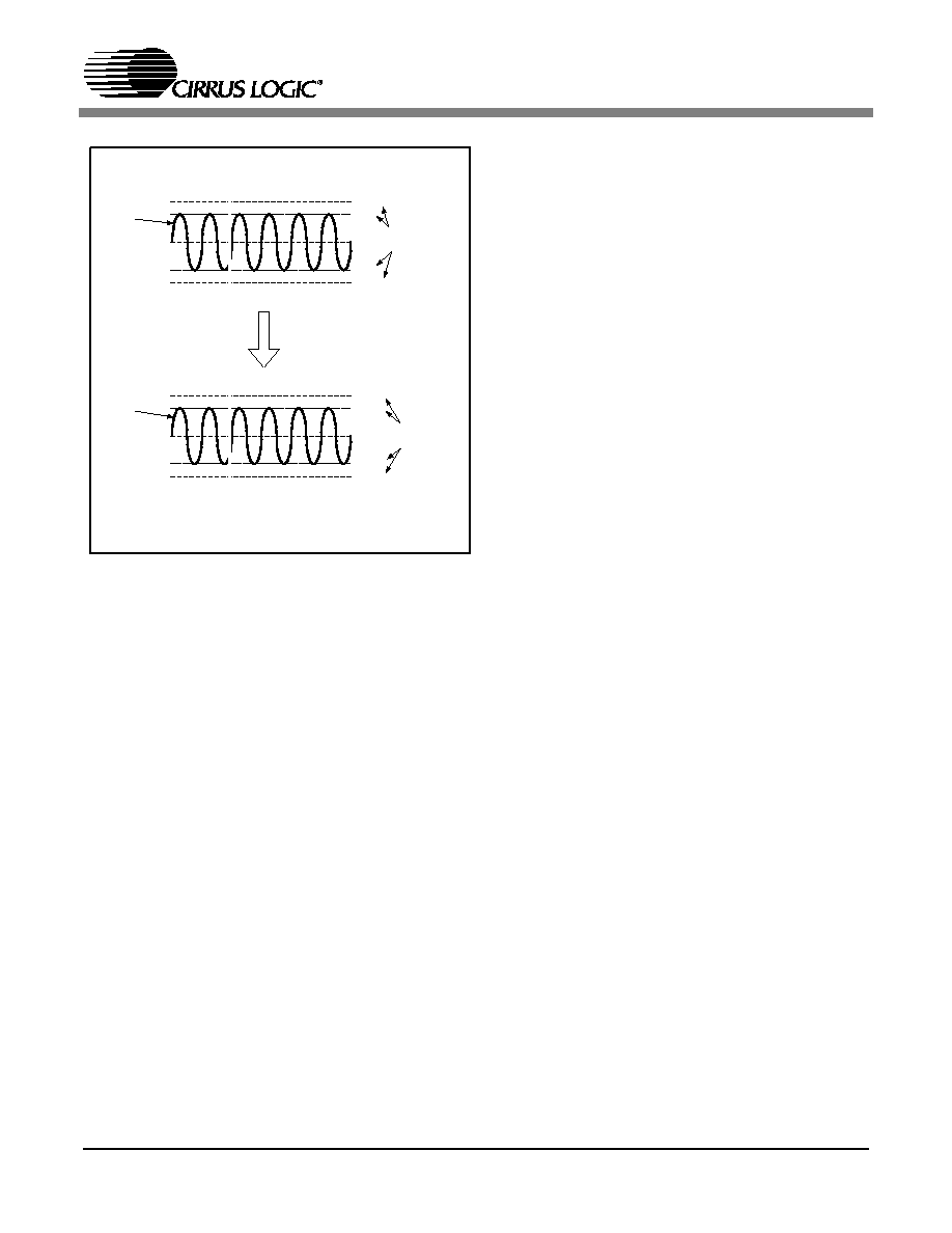
CS5460A
31
3.8.7.2 DC Offset Calibration Sequence
The Voltage Channel DC Offset Register holds the
negative of the simple average of N samples taken
while the DC voltage offset calibration was execut-
ed. The inputs should be grounded during DC off-
set calibration. The DC offset value is added to the
signal path to nullify the DC offset in the system.
3.8.7.3 AC Gain Calibration Sequence
The AC voltage gain calibration algorithm attempts
to adjust the Voltage Channel Gain Register value
such that the calibration reference signal level pre-
sented at the voltage inputs will result in a value of
0.6 in the RMS Voltage Register. The AC calibra-
tion signal is applied to the "+" and "-" input pins of
the channel under calibration. During AC voltage
gain calibration, the value in the RMS Voltage Reg-
ister is divided into 0.6. This result is the AC gain
calibration value stored in the Voltage Channel
Gain Register.
3.8.7.4 DC Gain Calibration Sequence
Based on the level of the positive DC calibration
voltage that should be applied across the "+" and
"-" inputs, the CS5460A determines the Voltage
Channel Gain Register value by averaging the In-
stantaneous Voltage Register's output signal val-
ues over one computation cycle (N samples) and
then dividing this average into 1. Therefore, after
the DC voltage gain calibration has been executed,
the Instantaneous Voltage Register will read
full-scale whenever the DC level of the input signal
is equal to the level of the DC calibration signal that
was applied to the voltage channel inputs during
the DC gain calibration. For example, if a +230 mV
DC signal is applied to the voltage channel inputs
during the DC gain calibration for the current chan-
nel, then the Instantaneous Voltage Register will
measure unity whenever a 230 mV DC level is ap-
plied to the voltage channel inputs.
3.8.8 Duration of Calibration Sequence
The value of the Cycle Count Register (N) deter-
mines the number of conversions that will be per-
formed by the CS5460A during a given calibration
sequence. For DC offset/gain calibrations, the cal-
ibration sequence always takes at least N + 30
conversion cycles to complete. For AC offset/gain
calibrations, the calibration sequence takes at
least 6N + 30 A/D conversion cycles to complete,
(about 6 computation cycles). If N is increased, the
accuracy of calibration results will increase.
For more information on Calibration, see
AN227,
"CALIBRATING THE CS5460A".
3.9 Phase Compensation
The values of bits 23 to 17 in the Configuration
Register can be altered to adjust the amount of
time delay that is imposed on the digitally sampled
voltage channel signal. This time delay is applied
to the voltage channel signal in order to compen-
sate for the relative phase delay (with respect to
the fundamental frequency) between the sensed
voltage and current signals. Voltage and current
transformers, as well as other sensor/filter/protec-
tion devices deployed at the front-end of the volt-
age/current sensor networks can often introduce a
phase-delay in the system that distorts/corrupts
the phase relationship between the line-voltage
and line-current signals that are to be measured.
The phase compensation bits PC[6:0] in the Con-
figuration Register can be set to nullify this undesir-
able phase distortion between the digitally
sampled signals in the two channels. The value in
the 7-bit phase compensation word indicates the
amount of time delay that is imposed on the volt-
V
RMS
Register =
230
/
250
x
1
/
2
0.65054
250 mV
230 mV
0 V
-230 mV
-250 mV
0.9999...
0.92
-0.92
-1.0000...
V
RMS
Register =
0.6000...
250 mV
230 mV
0 V
-230 mV
-250 mV
0.84853
-0.84853
Before AC Gain Calibration (Vgain Register = 1)
After AC Gain Calibration (Vgain Register changed to ~0.9223)
Instantaneous Voltage
Register Values
Instantaneous Voltage
Register Values
Sinewave
Sinewave
0.92231
-0.92231
INPUT
SIGNAL
INPUT
SIGNAL
Figure 19. Example of AC Gain Calibration

CS5460A
32
age channel's analog input signal
with respect to
the current channel's analog input signal.
With the default setting, the phase delay on the
voltage channel signal is ~0.995 µs (~0.0215 de-
grees assuming a 60 Hz power signal). With
MCLK = 4.096 MHz and K = 1, the range of the in-
ternal phase compensation ranges from
-2.8 degrees to +2.8 degrees when the input volt-
age/current signals are at 60 Hz. In this condition,
each step of the phase compensation register (val-
ue of one LSB) is ~0.04 degrees. For values of
MCLK other than 4.096 MHz, these values for the
span (-2.8 to +2.8 degrees) and for the step size
(0.04 degrees) should be scaled by
4.096 MHz / (MCLK / K). For power line frequen-
cies other than 60Hz (e.g., 50 Hz), the values of
the range and step size of the PC[6:0] bits can be
determined by converting the above values to
time-domain (seconds), and then computing the
new range and step size (in degrees) with respect
to the new line frequency.
Unlike offset/gain calibration, the CS5460A does
not provide an automated on-chip phase calibra-
tion sequence. To calibrate the phase delay, the
phase compensation bits can be adjusted while the
CS5460A is running in `continuous computation
cycles' data acquisition mode. For example, the
CS5460A can be set up to perform continuous
computations on a
purely resistive load (no induc-
tance or capacitance). The PC[6:0] bits can then
be adjusted until the Energy Register value is max-
imized.
3.10 Time-Base Calibration Register
The Time-Base Calibration Register (notated as
"TBC" in Figure 3) is used to compensate for slight
errors in the XIN input frequency. External oscilla-
tors and crystals have certain tolerances. If there is
a concern about improving the accuracy of the
clock for energy measurements, the Time-Base
Calibration Register value can be manipulated to
compensate for the frequency error. Note from Fig-
ure 3 that the TBC Register only affects the value
in the Energy Register.
As an example, if the desired XIN frequency is
4.096 MHz, but during production-level testing,
suppose that the average frequency of the crystal
on a particular board is measured to actually be
4.091 MHz. The ratio of the desired frequency to
the actual frequency is 4.096 MHz/4.091 MHz =
~1.00122219506. The TBC Register can be set to
1.00122213364 = 0x80280C(h), which is very
close to the desired ratio.
3.11 Power Offset Register
Referring to Figure 3, note the "P
off
" Register that
appears just after the power computation. This reg-
ister can be used to offset system power sources
that may be resident in the system, but do not orig-
inate from the power line signal. These sources of
extra energy in the system contribute undesirable
and false offsets to the power/energy measure-
ment results. For example, even after DC offset
and AC offset calibrations have been run on each
channel, when a voltage signal is applied to the
voltage channel inputs and the current channel is
grounded (i.e., there is zero input on the current
channel), the current channel may still register a
very small amount of RMS current caused by leak-
age of the voltage channel input signal into the cur-
rent channel input signal path. Although the
CS5460A has high channel-to-channel crosstalk
rejection, such crosstalk may not totally be elimi-
nated.) If the amount of `artificial' power that might
be induced into the voltage/current channel signals
due to such crosstalk/system noise/etc. can be de-
termined, then the Power Offset Register can be
programmed to nullify the effects of this unwanted
energy.
3.12 Input Protection - Current Limit
In Figures 6, 7, 8, and 9, note the series resistor R
I+
which is connected to the IIN+ input pin. This resis-
tor serves two purposes. First, this resistor func-
tions in coordination with C
Idiff
and/or C
Idiff
to form a
low-pass filter. The filter will a) remove any broad-
band noise that is far outside of the frequency
range of interest, and also b) this filter serves as
the
anti-aliasing filter, which is necessary to pre-
vent the A/D converter from receiving input signals
whose frequency is higher than one-half of the
sampling frequency (the Nyquist frequency). The
second purpose of this resistor is to provide cur-
rent-limit protection for the Iin+ input pin, in the
event of a power surge or lightning surge. The role
that R
I+
contributes to input filtering will be dis-
cussed in the Section 3.13. But first the current-lim-
it protection requirements for the Iin+/Iin- and
Vin+/Vin- pins are discussed.

CS5460A
33
The voltage/current-channel inputs have
surge-current limits of 100 mA. This applies to brief
voltage/current spikes (<250 ms). The limit is
10 mA for DC input overload situations. To prevent
permanent damage to the CS5460A, the designer
must include adequate protection circuitry in the
power meter design, to insure that these pin cur-
rent limits are never exceeded, when CS5460A is
operating in the intended power-line metering envi-
ronment.
Focusing specifically on Figure 7, which shows
how voltage/current transformers can be used to
sense the line-voltage/line-current, suppose for ex-
ample that the requirements for a certain 120 VAC
power system require that the power meter must
be able to withstand up to a 8 kV voltage spike on
the power line during normal operating conditions.
To provide a suitable sensor voltage input level to
the voltage channel input pins of the CS5460A, the
turns ratio of the voltage-sense transformer should
be chosen such that the ratio is, for example, on
the order of 1000:1. A voltage-sense transformer
with a 1000:1 turns ratio will provide a 120 mV
(rms) signal to the CS5460A's differential voltage
channel inputs, when the power line voltage is at
the nominal level of 120 VAC. Therefore, a brief
8 kV surge would be reduced to a 8 V surge across
R
V+
.
What happens when 8 volts (common-mode) is
present across one of the analog input pins of the
CS5460A? The Vin+/Vin- and Iin+/Iin- pins of the
CS5460A are equipped with internal protection di-
odes. If a voltage is presented to any of these pins
that is larger than approximately 7 V (with respect
to VA- pin) these protection diodes will turn on in-
side the CS5460A. But in order to prevent exces-
sive current levels from flowing through the device,
the value of R
V+
must be large enough that when a
8V surge is present across the secondaries of the
voltage-sense transformer, the brief surge current
through R
V+
should not be any greater than
100 mA. Therefore, a minimum value for R
V+
would be (8 V - 7 V) / 100 mA = 10
. This value
may be increased as needed, to easily obtain the
desired cutoff frequency of the anti-aliasing filter on
the voltage channel (described later), and also to
provide some margin. But the designer should try
to avoid using values for the protection resistors
that are excessively high. A typical value for R
V+
would be 470
.
The VIN- pin should also have a protection resistor
(called R
V-
in Figure 7). To maintain symmetry, the
value of R
V-
should be made equal to R
V+
.
For the current channel inputs (Iin+ and Iin-), if the
maximum current rating (I
max
) for this power line is
30 A (RMS), then a suitable turns ratio for the cur-
rent-sense transformer might be 200:1. Since the
maximum load for a 120 VAC line rated at 30 A
would be 4
(for unity power factor), a brief 8 kV
surge across "L" and "N" could generate as much
as 2000 A (RMS) of current through the primaries
of the current-sense transformer. This can in turn
generate as much as 10 V across the secondaries
of the current-sense transformer. This voltage is
high enough to turn on one or more of the internal
protection diodes located off of the Iin+/Iin- pins.
Therefore, the value of the protection resistor that
will limit the current flow to less than 100 mA would
be (10 V - 7 V) / 100 mA = 30
. In order to pro-
vide some margin and to use the same resistor val-
ues that are used on the Vin+/Vin- pins, a 470
resistor can be used as a lower limit for the R
I+
and
R
I-
resistors shown in Figure 7.
Referring to the circuit implementations shown in
Figures 6, 8, and 9, note that when resistor-divider
configurations are used to provide the voltage
channel sense voltage, the VIN+ pin does not need
an additional, separate, dedicated protection resis-
tor. This is because the resistive voltage-divider al-
ready provides the series resistance that is needed
for this protection resistance (from R
1
and R
2
).
(And note in Figure 8 that this is true for both the
VIN+ pin and the VIN- pin.) In Figure 7, a voltage
transformer is used as the voltage sensor. When
any type of transformer is used as the sensor de-
vice for voltage (or current) channel, a dedicated
protection resistor R
V+
should be installed in series
with the VIN+ pin, and similarly, a resistor (R
V-
)
should be installed in series to the VIN- input pin.
Additional considerations/techniques regarding
the protection of the analog input pins against sud-
den high-frequency, high-level voltage/current
surges are discussed in Section 3.14.

CS5460A
34
3.13 Input Filtering
Figure 6 shows how the analog inputs can be con-
nected for a
single-ended input configuration. Note
here that the Vin- and Iin- input pins are held at a
constant DC common-mode level, and the varia-
tion of the differential input signal occurs only on
the Vin+ and Vin- pins. The common-mode level
on the Vin-/Iin- pins is often set at (or very near) the
CS5460A's common-mode ground reference po-
tential. (The common-mode ground reference po-
tential is defined by the voltage at the VA- pin.)
But this is not required--the DC reference level of
the Vin-/Iin- pins can be set to any potential be-
tween [VA-] and [(VA+) - 250 mV]. In Figure 6, ob-
serve the circuitry which has been placed in front
of the current channel input pins, as one example.
The anti-aliasing filter can be constructed by calcu-
lating appropriate values for R
I+
= R
I-
, C
Idiff
, and
C
I+ =
C
I-
. The sensor voltage that is created by the
voltage drop across R
SHUNT
is fed into the Iin+ pin,
while the voltage at the Iin- pin is held constant.
Figure 7 shows a
differential bipolar input configu-
ration. Note in Figure 7 that the "+" and "-" input
pins for the voltage/current channels are equally
referenced above and below the CS5460A's
ground reference voltage. Such a differential bipo-
lar input configuration can be used because the
CS5460A voltage/current channel inputs are able
to accept input voltage levels as low as -250 mV
(common-mode) below the VA- pin ground refer-
ence, which is defined by the voltage at the VA-
pin. (In fact, if desired, the center-tapped reference
of these differential input pairs could be connected
to a DC voltage of, for example, +2 V, because
+2 V is within the available common-mode range
of [VA-] and [VA+ - 250mV]. But this configuration
may not be practical for most metering applica-
tions.) In the differential bipolar input configuration,
the voltage signals at the Vin- and Iin- pins will fluc-
tuate in similar fashion to the Vin+/Iin+ pins, except
the voltages at the "-" pins will be 180 degrees out
of phase with respect to the voltage signals at the
"+" pins. Therefore the signal paths to the "+" and
"-" pins play an equal role in defining the differential
voltage input signal. Because of this, the protection
resistors placed on Vin-/Iin- pins will play an equal-
ly important role as the resistors on the Vin+/Iin+
pins, in defining the differential responses of the
voltage/current channel input anti-aliasing filters.
These resistors also serve as the current-limit pro-
tection resistors (mentioned earlier).
Before determining a typical set of values for R
V+
,
R
V-
, C
V+
, C
V-
, C
Vdiff
, R
I+
, R
I-
, C
I+
, C
I-
, and C
Idiff
in
Figure 7, several other factors should be consid-
ered:
1. Values for the above resistors/capacitors should
be chosen with the desired differential-mode (and
common-mode) lowpass cutoff frequencies in
mind. In general, the differential cutoff frequencies
should not be less than 10 times the cut-off fre-
quencies of the internal voltage/current channel fil-
ters, which can be estimated by studying Figure 4
and Figure 5. In these figures, the internal voltage
channel cutoff frequency is ~1400 Hz while the
current channel cutoff frequency is ~1600 Hz. If
the cutoff frequency of the external anti-aliasing fil-
ter is much less than 10x these values (14000 Hz
and 16000 Hz), then some of the harmonic content
that may be present in the voltage/current signals
will be attenuated by the voltage/current channel
input anti-aliasing filters, because such R-C filters
will begin to roll off at a frequency of 1/10th of the
filter's -3 dB cutoff frequency. If the designer is not
interested in metering energy that may be present
in the higher harmonics (with respect to the funda-
mental power line frequency) then the differen-
tial-mode cutoff frequencies on the voltage/current
input networks can be reduced. However, relaxing
the metering bandwidth is usually unacceptable,
as most modern power meters are required to reg-
ister energy out to the 11th harmonic (at a mini-
mum).
2. The first-order time-constants of the overall volt-
age and current channel sensor networks should
be set such that they are equal (within reason), or
at least close in magnitude. If the time-constants of
the voltage/current sensor networks are not
well-matched, then the phase relationship be-
tween the voltage-sense and current-sense sig-
nals will suffer an undesirable shift. In this
situation, the real (true) power/energy measure-
ments reported by the CS5460A can contain signif-
icant error, because the power factor of the sensed
voltage and current signals will be significantly dif-
ferent than the actual power factor of the power
line voltage/current waveforms.

CS5460A
35
Note also that in addition to the time-constants of
the input R-C filters, the phase-shifting properties
of the voltage/current sensors devices may also
contribute to the overall time-constants of the volt-
age/current input sensor networks. For example,
current-sense transformers and potential trans-
formers can impose phase-shifts on the sensed
current/voltage waveforms. Therefore, this possi-
ble source of additional phase-shift caused by sen-
sor devices may also need to be considered while
selecting the final R and C values for the volt-
age/current anti-aliasing filters. As an alternative
to, or in addition to the fine adjustment of the R and
C values of the two anti-alias filters, the CS5460A's
phase compensation bits (see
Phase Compensa-
tion) can also be adjusted, in order to more closely
match the overall time-constants of the volt-
age/current input networks. Regardless of whether
the phase compensation bits are or are not used to
help more closely match the time-constants, this
requirement of equal time-constants must ulti-
mately be considered when selecting the final R
and C values that will be used for the input filters.
(Of course, this factor may not turn out to be so im-
portant if the designer is confident that the
mis-match between the voltage/current channel
time-constants will not cause enough error to vio-
late the accuracy requirements for the given pow-
er/energy metering application.)
3. Referring to the specs in
Section 1, note that the
differential input impedance across the current
channel input pins is only 30 k
, which is signifi-
cantly less than the corresponding impedance
across the voltage channel input pins (which is
1 M
). While the impedance across the voltage
channel is usually high enough to be ignored, the
impedance across the current channel inputs may
need to be taken into account by the designer
when the desired cutoff frequencies of the filters
(and the time-constants of the overall input net-
works) are computed. Also, because of this rather
low input impedance across the current channel in-
puts, the designer should note that as the values
for R
I+
and/or R
I-
are increased, the interaction of
the current channel's input impedance can begin to
cause a significant voltage drop within the current
channel input network. If this is not taken into ac-
count, values may be chosen for R
I+
= R
I-
that are
large enough to cause a discrepancy between the
expected (theoretical) sensor gain and the
actual
sensor gain of the current sensor network, which
may not be anticipated by the designer. Also, if this
voltage drop effect is not considered, the designer
may select values for R
I+
and R
I
that are slightly
larger than they should be, in terms of maximizing
the available dynamic range of the current channel
input. For the very same reason, the line-cur-
rent-to-sensor-output-voltage conversion factor of
the current sensor may not be optimized if this volt-
age division is not considered, when (for example)
selecting a value for the burden resistor for a given
current transformer. This issue should be consid-
ered, although a slight voltage drop only causes a
slight loss in available dynamic range, and the ef-
fects of this voltage drop on the actual current
channel sensor gain can be removed during gain
calibration of the current channel.
4. Referring to Figures 6 - 9, not all of the capaci-
tors/resistors shown in these example circuit dia-
grams are necessary; however, note that the all of
the filter capacitors (C
V+
, C
V-
, C
I+
, C
I-
, C
Vdiff
, and C
I-
diff
) can, in some situations, help to improve the
ability of both input networks to attenuate very
high-frequency RFI that can enter into the
CS5460A's analog input pins. Therefore, during
layout of the PCB, these capacitors should be
placed in close proximity to their respective input
pins.
If any/all of the common-mode connected capaci-
tors (C
V+
, C
V-
, C
I+
, C
I-
) are included in the input net-
works, their values should be selected such that
they are at least one order of magnitude
smaller
than the value of the differential capacitors (C
Vdiff
,
and C
Idiff
). This is done for at least two reasons:
a) The value tolerance for most types of commer-
cially available surface-mount capacitors is not
small enough to insure appreciable value match-
ing, between the value of C
V+
vs. C
V-
, as well as
between the value of C
V+
vs. C
V-
. Such value mis-
match can adversely affect the desired differen-
tial-mode response of the voltage/current input
networks. By keeping the values of these com-
mon-mode capacitors small, and allowing the val-
ue of the C
Vdiff
, and C
Idiff
to dominate the
differential 1st-order time-constant of the input filter
networks, this undesirable possibility of frequency
response variation can be minimized.

CS5460A
36
b) The common-mode rejection performance of the
CS5460A is sufficient within the frequency range
over which the CS5460A performs A/D conver-
sions. Addition of such common-mode caps can
actually often degrade the common-mode rejec-
tion performance of the entire voltage/current input
networks. Therefore, choosing relatively small val-
ues for (C
V+
, C
V-
, C
I+
, C
I-
) will provide necessary
common-mode rejection at the much higher fre-
quencies, and will allow the CS5460A to realize its
CMRR performance in the frequency-range of in-
terest.
[Note that this discussion does not include correc-
tion of phase-shifts caused by the voltage-sense
transformer and current-sense transformer, al-
though these phase-shifts should definitely be con-
sidered in a real-life practical meter design.] On the
current channel, using commonly available values
for the components, R
I+
and R
I-
can be set to
470
. Then a value of C
Idiff
= 18 nF and a value of
0.22 nF for C
I-
and C
I-
will yield a -3 dB cutoff fre-
quency of 15341 Hz for the current channel. For
the voltage channel, if R
I+
and R
I-
are also set to
470
, C
Vdiff
= 18 nF, and C
V-
= C
V-
= 0.22 nF
(same as current channel), the -3 dB cutoff fre-
quency of the voltage channel's input filter will be
14870 Hz. The difference in the two cutoff frequen-
cies is due to the difference in the input impedance
between the voltage/current channels.
If there is concern about the effect that the differ-
ence in these two cutoff frequencies (and therefore
the mis-match between the time-constants of the
overall voltage/current input networks) would have
on the accuracy of the power/energy registration, a
non-standard resistor value for R
V+
= R
V-
of (for ex-
ample) 455
can be used. This would shift the
(differential) -3 dB cutoff frequency of the voltage
channel's input filter (at the voltage channel inputs)
to ~15370 Hz, which would cause the first-order
time-constants of the voltage/current channel input
filters to be closer in value.
Agreement between the voltage/current channel
time-constants can also be obtained by adjusting
the phase compensation bits, instead of using less
commonly-available resistor/capacitor values
(such as R
I+
= R
I-
= 455
). If the values of R
I+
and
R
I-
are again 470
, the first-order time-constants
of the two R-C filters are estimated by taking the re-
ciprocal of the -3 dB cutoff frequencies (when ex-
pressed in rads/s). Subtracting these two
time-constants shows that after the voltage/current
signals pass through their respective anti-aliasing
filters, the sensed voltage signal will be delayed
~0.329 µs more than the current signal. If metering
a 60 Hz power system, this implies that the input
voltage-sense signal will be delayed
~0.007 degrees more than the delay imposed on
the input current-sense signal. Note that when the
PC[6:0] bits are set to their default setting of
"0000000", the internal filtering stages of the
CS5460A will impose an additional delay on the
fundamental frequency component of the 60Hz
voltage signal of 0.0215 degrees, with respect to
the current signal. The total difference between the
delay on the voltage-sense fundamental and the
current-sense fundamental will therefore be
~0.286 degrees. But if the phase compensation
bits are set to 1111111, the CS5460A will delay the
voltage channel signal by an additional -0.04 de-
grees, which is equivalent to shifting the voltage
signal
forward by 0.04 degrees. The total phase
shift on the voltage-sense signal (with respect to
the fundamental frequency) would then be
~0.011 degrees ahead of the current-sense signal,
which would therefore provide more close-
ly-matched delay values between the volt-
age-sense and current-sense signals. Adjustment
of the PC[6:0] bits therefore can provide an effec-
tive way to more closely match the delays of the
voltage/current sensor signals, allowing for more
commonly available R and C component values to
be used in both of these filters.
As a final note, tolerances of the R and C compo-
nents that are used to build the two R-C filters
should also be taken into consideration. A com-
mon tolerance of ±0.1% can vary the delay by as
much as much as ~±2.07 µs, which means that the
difference between the delays of the voltage-sense
and current-sense signals that is caused by these
filters could vary by as much as ~±4.1 µs, which is
equivalent to a phase shift of ~±0.089 degrees (at
60 Hz). This in turn implies that our decision to ad-
just the PC[6:0] bits (to shift the voltage signal for-
ward by 0.04 degrees) could actually cause the
voltage signal to be shifted by as much as
~0.100 degrees ahead of the current signal.
Thus, adjustment of the PC[6:0] bits to more close-
ly match the two time-constants/delays may only
be useful if a precise calibration operation can be
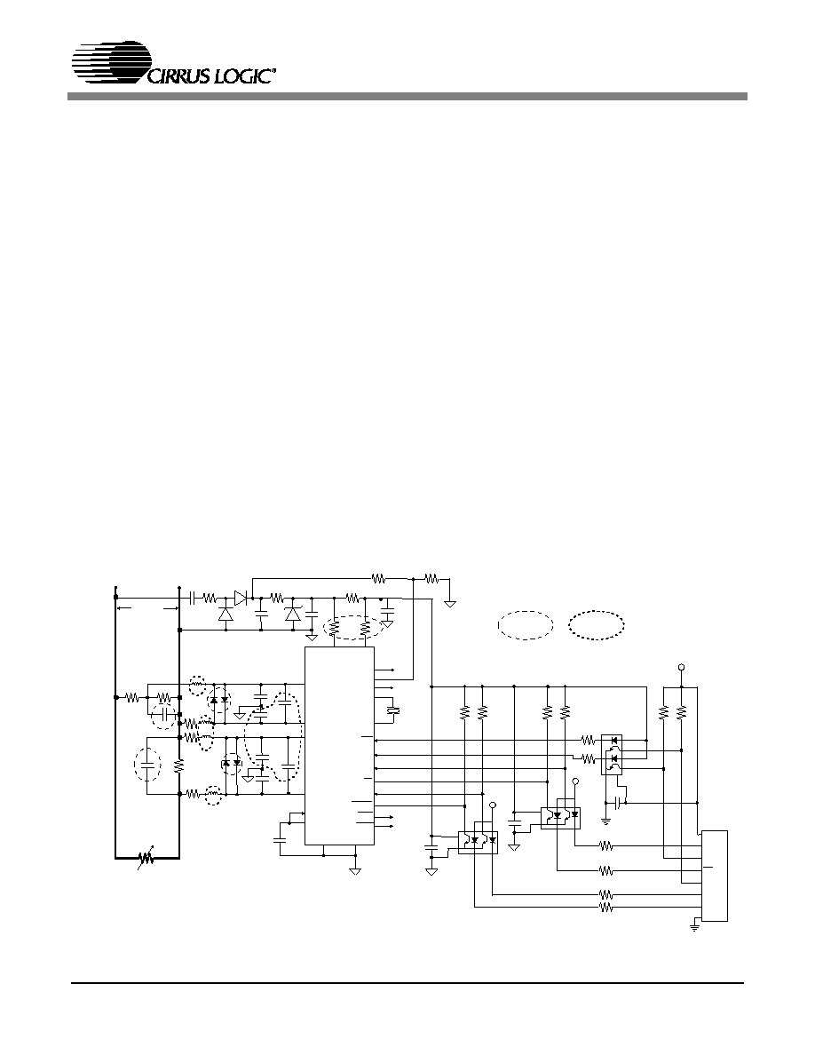
CS5460A
37
performed on
each individual power meter, during
final calibration/test of the meter.
3.14 Protection Against High-Voltage
and/or High-Current Surges
In many power distribution systems, it is very likely
that the power lines will occasionally carry brief but
large transient spikes of voltage/current. Two com-
mon sources of such high-energy disturbances are
1) a surge in the line during a lightning storm, or 2)
a surge that is caused when a very inductive or ca-
pacitive load on the power line is suddenly turned
on ("inductive kick"). In these situations, the input
protection resistors and corresponding input filter
capacitors (discussed in the previous sections)
may not be sufficient to protect the CS5460A from
such high-frequency voltage/current surges. The
surges may still be strong enough to cause perma-
nent damage to the CS5460A. Because of this, the
designer should consider adding certain additional
components within the voltage/current channel in-
put circuitry, which can help to protect the
CS5460A from being permanently damaged by the
surges.
Referring to Figure 20, the addition of capacitors
C1 and C2 can help to further attenuate these
high-frequency power surges, which can greatly
decrease the chances that the CS5460A will be
damaged. Typical values for C1 and C2 may be on
the order of 10 pF, although the exact value is re-
lated to the reactive and resistive properties of the
voltage and current sensor devices. In addition, di-
odes D1 - D4 can help to quickly clamp a high volt-
age surge voltage presented across the
voltage/current inputs, before such a surge can
damage the CS5460A. An example of a suitable
diode part number for this application is BAV199,
which has the ability to turn on very quickly (very
small turn-on time). A fuse could potentially serve
this purpose as well (not shown). R3 and R4 can
provide protection on the "-" sides of the two input
pairs. Set R3 = R1 and R4 = R5. Finally, placing
50
resistors in series with the VA+ and VD+ pins
is another technique that has sometimes proven to
be effective in protecting the CS5460A from such
high-level, high-frequency voltage/current surges.
However, these 50
resistors may not be neces-
sary if the protection on the analog input channels
is sufficient, and this is not the most attractive so-
VA+
VD+
CS5460A
0.1 µF
100 µF
500
470 nF
500
N
10
14
VIN+
9
VIN-
IIN-
10
15
16
IIN+
PFMON
CPUCLK
XOUT
XIN
RESET
17
2
1
24
19
CS
7
SDI
23
SDO
6
SCLK
5
INT
20
EDIR
22
EOUT
21
0.1 µF
VREFIN
12
VREFOUT
11
VA-
DGND
13
4
3
0.1 µF
10 k
5 k
L
R
L
4.069 MHz
To Service
1 k
1 k
1 k
1 k
+5 V
+5 V
10 k 10 k
47 k
47 k
20 k 20 k
1 k
SCLK
SDO
CS
INT
SDI
RST
GND
+5 V
5.1 Volt
1 k
120 Vrms
50
50
For Input Surge
Protection
To reduce
EMI susceptibility
D1
D2
D4
D3
R3
R4
C1
C2
R1
R2
R
SHUNT
R5
C4
C5
C6
C7
C3
C8
MODE
NC
8
NC
L3
L4
L1
L2
Figure 20. Input Protection for Single-Ended Input Configurations
Input protection for single-ended input configurations, using resistive
divider and current shunt resistor.
Note that the digital interface is isolated using opto-isolators.

CS5460A
38
lution, because these resistors will dissipate what
can be a significant amount of power, and they will
cause an undesirable voltage drop which decreas-
es the voltage level presented to the VA+ and VD+
supply pins.
3.15 Improving RFI Immunity
During EMC acceptance testing of a power meter-
ing assembly, the performance of the CS5460A's
A/D converters can be adversely affected by exter-
nal radio frequency interference (RFI). Such exter-
nal RFI can be coupled into the copper traces
and/or wires on the PCB. If RFI is coupled into any
of the traces which tie into the CS5460A's
Vin+/Vin- or Iin+/Iin- input pins, then errors may be
present in the CS5460A's power/energy registra-
tion results.
When such degradation in performance is detect-
ed, the CS5460A's immunity to RF disturbance
may be improved by configuring the `+' and `-' in-
puts of the voltage/current channel inputs such that
they are more symmetrical. This is illustrated in
Figure 20 with the addition of resistors R3 and R4,
as well as capacitors C5 and C6. Note that the in-
put circuitry placed in front of the voltage/current
channel inputs in Figure 20 represents a
sin-
gle-ended input configurations (for both channels).
Therefore, these extra resistors and components
may not necessarily be needed to achieve the sim-
ple basic anti-aliasing filtering on the inputs. How-
ever, the addition of these extra components can
create more symmetry across the `+' and `-' inputs
of the voltage/current input channels, which can of-
ten help to reduce the CS5460A's susceptibility to
RFI. The value of C5 should be the same as C3,
(and so the designer may have to re-calculate the
desired value of C3, since the addition of C5 will
change the overall differential-/common-mode fre-
quency responses of the input filter.) A similar ar-
gument can be made for the addition of C6 (to
match C8) on the current channel's input filter. Fi-
nally, addition of capacitors C4 and C7 can also
sometimes help to improve CS5460A's perfor-
mance in the presence of RFI. All of these input ca-
pacitors (C3 - C8) should be placed in very close
proximity to the `+' and `-' pins of the voltage/cur-
rent input pins in order to maximize their ability to
protect the input pins from high-frequency RFI. In
addition to or as an alternative to these capacitors,
addition of inductors L1 - L4 can sometimes help to
suppress any incoming RFI. Note that the addition-
al components just discussed can sometimes actu-
ally
degrade the CS5460A's immunity to RFI. The
exact configuration that works best can vary signif-
icantly, according to the exact PCB layout/orienta-
tion. Finally, note that inside the CS5460A, the
Vin+, Vin-, Iin+, and Iin- pins have all been buffered
with ~10 pF of internal capacitance (to VA-) in at-
tempt to improve the device's immunity to external
RFI.
3.16 PCB Layout
For optimal performance, the CS5460A should be
placed entirely over an analog ground plane with
both the VA- and DGND pins of the device con-
nected to the analog plane.
Note: Refer to the CDB5460A Evaluation Board for
suggested layout details, as well as
Applications Note 18 for more detailed layout
guidelines. Before layout, please call for our
Free Schematic Review Service.
4. SERIAL PORT OVERVIEW
The CS5460A's serial port incorporates a state
machine with transmit/receive buffers. The state
machine interprets 8 bit command words on the
rising edge of SCLK. Upon decoding of the com-
mand word, the state machine performs the re-
quested command or prepares for a data transfer
of the addressed register. Request for a read re-
quires an internal register transfer to the transmit
buffer, while a write waits until the completion of
24 SCLKs before performing a transfer. The inter-
nal registers are used to control the ADC's func-
tions. All registers are 24-bits in length. Figure 21,
in section 5, summarizes the internal registers
available.
The CS5460A is initialized and fully operational in
its
active state upon power-on. After a power-on,
the device will wait to receive a valid command (the
first 8-bits clocked into the serial port). Upon re-
ceiving and decoding a valid command word, the
state machine instructs the converter to either per-
form a system operation, or transfer data to or from
an internal register.

CS5460A
39
4.1 Commands (Write Only)
All command words are 1 byte in length. Commands that write to a register must be followed by 3 bytes of register
data. Commands that read from registers initiate the output of 3 bytes of register data. Commands that read data
can be `chained' with other commands (e.g., while reading data, a new command can be sent to SDI which can ex-
ecute before the original read is completed). This allows for `chaining' commands.
4.1.1 Start Conversions
This command indicates to the state machine to begin acquiring measurements and calculating results. The device
has two modes of acquisition.
Modes of acquisition/measurement
0 = Perform a single computation cycle
1 = Perform continuous computation cycles
4.1.2 SYNC0 Command
This command is the end of the serial port re-initialization sequence. It can also be used as a NOP command. The
serial port is resynchronized to byte boundaries by sending three or more consecutive SYNC1 commands followed
by a SYNC0 command.
4.1.3 SYNC1 Command
This command is part of the serial port re-initialization sequence. It can also serve as a NOP command.
4.1.4 Power-Up/Halt
If the device is powered-down into either
stand-by
or
sleep
power saving mode (See
4.1.5
), this command will pow-
er-up the device. After the CS5460A is initially powered-on, no conversions/computations will be running. If the de-
vice is already powered on and the device is running either `single computation cycle' or `continuous computation
cycles' data acquisition modes, all computations will be halted once this command is received.
B7
B6
B5
B4
B3
B2
B1
B0
1
1
1
0
C
0
0
0
B7
B6
B5
B4
B3
B2
B1
B0
1
1
1
1
1
1
1
0
B7
B6
B5
B4
B3
B2
B1
B0
1
1
1
1
1
1
1
1
B7
B6
B5
B4
B3
B2
B1
B0
1
0
1
0
0
0
0
0

CS5460A
40
4.1.5 Power-Down
The device has two power-down states to conserve power. If the chip is put in stand-by state, all circuitry except the
analog/digital clock generators is turned off. In the sleep state, all circuitry except the digital clock generator and the
instruction decoder is turned off. Waking up the CS5460A out of sleep state requires more time than waking the
device out of stand-by state, because of the extra time needed to re-start and re-stabilize the analog clock signal.
[S1 S]0
Power-down state
00 = Reserved
01 = Halt and enter stand-by power saving state. This state allows quick power-on time
10 = Halt and enter sleep power saving state. This state requires a slow power-on time
11 = Reserved
4.1.6 Calibration
The device has the capability of performing a system AC offset calibration, DC offset calibration, AC gain calibration,
and DC gain calibration. Calibration can be done on the voltage channel, the current channel, or both channels at
the same time. Offset and gain calibrations should NOT be performed at the same time (must do one after the oth-
er). For a given application, if DC gain calibrations are performed, then AC gain calibration should not be performed
(and vice-versa). The proper input voltages must be supplied to the device before initiating calibration.
[V I]
Designates calibration channel
00 = Not allowed
01 = Calibrate the current channel
10 = Calibrate the voltage channel
11 = Calibrate voltage and current channel simultaneously
R
Specifies AC calibration (R=1) or DC calibration (R=0)
G
Designates gain calibration
0 = Normal operation
1 = Perform gain calibration
O
Designates offset calibration
0 = Normal operation
1 = Perform offset calibration
B7
B6
B5
B4
B3
B2
B1
B0
1
0
0
S1
S0
0
0
0
B7
B6
B5
B4
B3
B2
B1
B0
1
1
0
V
I
R
G
O

CS5460A
41
4.1.7 Register Read/Write
This command informs the state machine that a register access is required. On reads the addressed register is load-
ed into the output buffer and clocked out by SCLK. On writes the data is clocked into the input buffer and transferred
to the addressed register on the 24
th
SCLK.
W/R
Write/Read control
0 = Read register
1 = Write register
RA[4:0]
Register address bits. Binary encoded 0 to 31. All registers are 24 bits in length.
Address
Abbreviation
Name/Description
00000
Config
Configuration Register.
00001
I
DCoff
Current Channel DC Offset Register.
00010
I
gn
Current Channel Gain Register.
00011
V
DCoff
Voltage Channel DC Offset Register.
00100
V
gn
Voltage Channel Gain Register.
00101
Cycle Count
Number of A/D cycles per computation cycle.
00110
Pulse-Rate
Used to set the energy-to-pulse ratio on EOUT (and EDIR).
00111
I
Instantaneous Current Register (most recent current sample).
01000
V
Instantaneous Voltage Register (most recent voltage sample).
01001
P
Instantaneous Power Register (most recent power sample).
01010
E
Energy Register (accumulated over latest computation cycle).
01011
I
RMS
RMS Current Register (computed over latest computation cycle).
01100
V
RMS
RMS Voltage Register (computed over latest computation cycle).
01101
TBC
Timebase Calibration Register.
01110
Poff
Power Offset Register.
01111
Status
Status Register.
10000
I
ACoff
Current Channel AC Offset Register.
10001
V
ACoff
Voltage Channel AC Offset Register.
10010
Res
Reserved
.
.
.
.
.
.
10111
Res
Reserved
11000
Res
Reserved
11001
Test
Reserved
11010
Mask
Mask Register.
11011
Res
Reserved
11100
Ctrl
Control Register.
11101
Res
Reserved
.
.
.
.
.
.
11111
Res
Reserved
These registers are for Internal Use only and should not be written to.
B7
B6
B5
B4
B3
B2
B1
B0
0
W/R
RA4
RA3
RA2
RA1
RA0
0

CS5460A
42
4.2 Serial Port Interface
The CS5460A's
slave-mode serial interface con-
sists of two control lines and two data lines, which
have the following pin-names: CS, SCLK, SDI,
SDO. Each control line is now described.
CS Chip Select (input pin), is the control line which
enables access to the serial port. When CS is set
to logic 1, the SDI, SDO, and SCLK pins will be
held at high impedance. When the CS pin is set to
logic 0, the SDI, SDO, and SCLK pins have the fol-
lowing functionality:
SDI Serial Data In (input pin), is the user-generat-
ed signal used to transfer (send) data/com-
mand/address/etc. bits into the device.
SDO Serial Data Out (output pin), is the data sig-
nal used to read output data bits from the device's
registers.
SCLK Serial Clock (input pin), is the serial
bit-clock which controls the transfer rate of data
to/from the ADC's serial port. To accommodate op-
to-isolators, SCLK is designed with a Schmitt-trig-
ger input to allow an opto-isolator with slower rise
and fall times to directly drive the pin. Additionally,
SDO is capable of sinking or sourcing up to 5 mA
to directly drive an opto-isolator LED. SDO will
have less than a 400 mV loss in the drive voltage
when sinking or sourcing 5 mA.
4.3 Serial Read and Write
The state machine decodes the command word as
it is received. Data is written to and read from the
CS5460A by using the Register Read/Write com-
mand. Figure 1 illustrates the serial sequence nec-
essary to write to or read from the serial port
buffers. As shown in Figure 1, a transfer of data is
always initiated by sending the appropriate 8-bit
command (MSB first) to the serial port (SDI pin). It
is important to note that some commands use in-
formation from the Cycle-Count Register and Con-
figuration Register to perform the function. For
those commands, it is important that the correct in-
formation is written to those registers first.
4.3.1 Register Write
When a command involves a write operation, the
serial port will continue to clock in the data bits
(MSB first) on the SDI pin for the next 24 SCLK cy-
cles. Command words instructing a register write
must be followed by 24 bits of data. For instance,
to write the Configuration Register, the command
(0x40) is transmitted to initiate a write to the Con-
figuration Register. The CS5460A will acquire the
serial data input from the SDI pin after 24 pulses
on the SCLK pin. Once the data is received, the
state machine writes the data to the Configuration
Register and then waits to receive another valid
command.
4.3.2 Register Read
When a read command is initiated, the serial port
will start transferring register content bits (MSB
first) on the SDO pin for the next 8, 16, or 24 SCLK
cycles. Command words instructing a register read
may be terminated at 8-bit boundaries (e.g., read
transfers may be 8, 16, or 24 bits in length). Also,
data register reads allow "command chaining", in
which the micro-controller is allowed to send a new
command while reading register data. The new
command will be acted upon immediately and
could possibly terminate the first register read. For
example, if a command word is sent to the state
machine to read one of the output registers, then
after pulsing SCLK for 16-bits of data, a second
write command word (e.g., to clear the Status Reg-
ister) may be pulsed on to the SDI line at the same
time the last 8-bits of data (from the first read com-
mand) are pulsed from the SDO line.
During the read cycle, the SYNC0 command
(NOP) should be strobed on the SDI port while
clocking the data from the SDO port.
4.4 System Initialization
A software or hardware reset can be initiated at
any time. The software reset is initiated by writing
a logic 1 to the RS (Reset System) bit in the Con-
figuration Register, which automatically returns to
logic 0 after reset. At the end of the 32
nd
SCLK
(i.e., 8 bit command word and 24 bit data word) in-
ternal synchronization delays the loading of the
Configuration Register by 3 or 4 DCLK cycles.
Then the reset circuit initiates the reset routine on
the 1
st
falling edge of MCLK.
A hardware reset is initiated when the RESET pin
is forced low for
at least 50 ns. The RESET signal
is asynchronous, requiring no MCLKs for the part
to detect and store a reset event. The RESET pin
is a Schmitt Trigger input, which allows it to accept

CS5460A
43
slow rise times and/or noisy control signals. (It is
not uncommon to experience temporary periods of
abnormally high noise and/or slow, gradual resto-
ration of power, during/after a power "black-out" or
power "brown-out" event.) Once the RESET pin is
de-asserted, the internal reset circuitry remains ac-
tive for 5 MCLK cycles to insure resetting the syn-
chronous circuitry in the device. The modulators
are held in reset for 12 MCLK cycles after RESET
is de-asserted. After a hardware or software reset,
the internal registers (some of which may drive out-
put pins) will be reset to their default values on the
first MCLK received after detecting a reset event
(see Table 3). The CS5460A will then assume its
active state. (The term active state, as well as the
other possible power states of the CS5460A, are
described in Section 4.6).
The reader should refer to Section 5 for a complete
description of the registers listed in Table 3.
4.5 Serial Port Initialization
It is possible for the serial interface to become un-
synchronized with respect to the SCLK input. If
this occurs, any attempt to clock valid CS5460A
commands into the serial interface will result in ei-
ther no operation or unexpected operation be-
cause the CS5460A will not interpret the input
command bits correctly. The CS5460A's serial port
must then be re-initialized. To initialize the serial
port, any of the following actions can be performed:
1) Power on the CS5460A. (Or if the device is al-
ready powered on, recycle the power.)
2) Hardware Reset.
3) Issue the
Serial Port Initialization Sequence,
which is performed by clocking 3 (or more)
SYNC1 command bytes (0xFF) followed by
one SYNC0 command byte (0xFE) to the serial
interface.
4.6 CS5460A Power States
Active state denotes the operation of CS5460A
when the device is fully powered on (i.e., not in
sleep state or stand-by state). Performing any of
the following actions will insure that the CS5460A
is operating in the
active state:
1) Power on the CS5460A. (Or if the device is al-
ready powered on, recycle the power.)
2) Hardware Reset
3) Software Reset
In addition to the three actions listed above, if the
device is operating in
sleep state or stand-by state,
waking up the device out of
sleep state or stand-by
state (by issuing the Power-Up/Halt command) will
also insure that the device is set into
active state.
But in order to send the Power-Up/Halt command
to the device, the serial port has to be initialized.
Therefore, successful wake-up of the device can
be insured by writing the serial port initialization se-
quence to the serial interface, prior to writing the
Power-Up/Halt command.
For a description of the
sleep power state and the
stand-by power state, see the Power Down Com-
mand, located in Section 4.1.
Configuration Register:
0x000001
DC offset registers:
0x000000
Gain registers
0x400000
Pulse-Rate Register:
0x0FA000
Cycle-Counter Register:
0x000FA0
Timebase Register:
0x800000
Status Register:
(see Section 5)
Mask Register:
0x000000
Control Register:
0x000000
AC offset registers:
0x000000
Power Offset Register:
0x000000
All data registers:
0x000000
All unsigned data registers
0x000000
Table 3. Default Register Values upon Reset Event

CS5460A
44
5. REGISTER DESCRIPTION
Note: 1. ** "default" => bit status after software or hardware reset
2. Note that all registers can be read from, and written to.
5.1 Configuration Register
Address: 0
Default** = 0x000001
K[3:0]
Clock divider. A 4 bit binary number used to divide the value of MCLK to generate the internal
clock DCLK. The internal clock frequency is DCLK = MCLK/K. The value of K can range be-
tween 1 and 16. Note that a value of "0000" will set K to 16 (not zero).
iCPU
Inverts the CPUCLK clock. In order to reduce the level of noise present when analog signals
are sampled, the logic driven by CPUCLK should not be active during the sample edge.
0 = normal operation (default)
1 = minimize noise when CPUCLK is driving rising edge logic
IHPF
Control the use of the High Pass Filter on the Current Channel.
0 = High-pass filter is disabled. If VHPF is set, use all-pass filter. Otherwise, no filter is used.
(default)
1 = High-pass filter is enabled.
VHPF
Control the use of the High Pass Filter on the voltage Channel.
0 = High-pass filter is disabled. If IHPF is set, use all-pass filter. Otherwise, no filter is used.
(default)
1 = High-pass filter enabled
23
22
21
20
19
18
17
16
PC6
PC5
PC4
PC3
PC2
PC1
PC0
Gi
15
14
13
12
11
10
9
8
EWA
Res
Res
SI1
SI0
EOD
DL1
DL0
7
6
5
4
3
2
1
0
RS
VHPF
IHPF
iCPU
K3
K2
K1
K0
Current
Channel
Voltage
Channel
Cycle-Counter Registe
Status Register (1 ◊ 24)
Serial Interface
Mask Register (1 ◊ 24)
Unsigned Output Registers (2 ◊ 24)
(I
, V
)
Command Word
State Machine
Transmit Buffer
Receive Buffer
Signed Output Registers (4 ◊ 24)
(I, V, P, E)
RMS
RMS
24-Bit
SDI
CS
SDO
SCLK
INT
AC Offset Register (1 x 24)
AC Offset Register (1 x 24)
Control Register (1 x 24)
Power Offset Register (1 x 24)
Configuration Register (1 ◊ 24)
Pulse-Rate Register (1 ◊ 24)
Offset Register (1 ◊ 24)
DC
Offset Register (1 ◊ 24)
DC
Gain Register (1 ◊ 24)
AC/DC
Gain Register (1 ◊ 24)
AC/DC
r (1 ◊ 24)
Timebase Cal. Register (1 x 24)
Figure 21. CS5460A Register Diagram

CS5460A
45
RS
Start a chip reset cycle when set 1. The reset cycle lasts for less than 10 XIN cycles. The bit is
automatically returned to 0 by the reset cycle.
DL0
When EOD = 1, EDIR becomes a user defined pin. DL0 sets the value of the EDIR pin.
Default = '0'
DL1
When EOD = 1, EOUT becomes a user defined pin. DL1 sets the value of the EOUT pin.
Default = '0'
EOD
Allows the EOUT and EDIR pins to be controlled by the DL0 and DL1 bits. EOUT and EDIR can
also be accessed using the Status Register.
0 = Normal operation of the EOUT and EDIR pins. (default)
1 = DL0 and DL1 bits control the EOUT and EDIR pins.
SI[1:0]
Soft interrupt configuration. Select the desired pin behavior for indication of an interrupt.
00 = active low level (default)
01 = active high level
10 = falling edge (INT is normally high)
11 = rising edge (INT is normally low)
Res
Reserved. These bits must be set to zero.
EWA
Allows the output pins of EOUT and EDIR of multiple chips to be connected in a wire-AND, us-
ing an external pull-up device.
0 = normal outputs (default)
1 = only the pull-down device of the EOUT and EDIR pins are active
Gi
Sets the gain of the current PGA
0 = gain is 10 (default)
1 = gain is 50
PC[6:0]
Phase compensation. A 2's complement number used to set the delay in the voltage channel.
When MCLK = 4.096 MHz and K = 1, the phase adjustment range is about -2.8 to +2.8 degrees
and each step is about 0.04 degrees (this assumes that the power line frequency is 60 Hz). If
(MCLK / K) is not 4.096 MHz, the values for the range and step size should be scaled by the
factor 4.096 MHz / (MCLK / K).
Default setting is 0000000 = 0.0215 degrees phase delay (when MCLK = 4.096 MHz).

CS5460A
46
5.2 Current Channel DC Offset Register and Voltage Channel DC Offset Register
Address:
1 (Current Channel DC Offset Register)
3 (Voltage Channel DC Offset Register)
Default** = 0.000
The DC offset registers are initialized to zero on reset, allowing the device to function and perform measure-
ments. The register is loaded after one computation cycle with the current or voltage offset when the proper input
is applied and the DC Calibration Command is received. DRDY will be asserted at the end of the calibration.
The register may be read and stored so the register may be restored with the desired system offset compensa-
tion. The value is in the range ± full scale. The numeric format of this register is two's complement notation.
5.3 Current Channel Gain Register and Voltage Channel Gain Register
Address:
2 (Current Channel Gain Register)
4 (Voltage Channel Gain Register)
Default** = 1.000
The gain registers are initialized to 1.0 on reset, allowing the device to function and perform measurements. The
gain registers hold the result of either the AC or DC gain calibrations, whichever was most recently performed.
If DC calibration is performed, the register is loaded after one computation cycle with the system gain when the
proper DC input is applied and the Calibration Command is received. If AC calibration is performed, then after
~(6N + 30) A/D conversion cycles (where N is the value of the Cycle-Count Register) the register(s) is loaded
with the system gain when the proper AC input is applied and the Calibration Command is received. DRDY will
be asserted at the end of the calibration. The register may be read and stored so the register may be restored
with the desired system offset compensation. The value is in the range 0.0
Gain < 4.0.
5.4 Cycle Count Register
Address: 5
Default** = 4000
The Cycle Count Register value (denoted as `N') specifies the number of A/D conversion cycles per
computation
cycle
. For each computation cycle, the updated results in the RMS and Energy Registers are computed using
the most recent set of N continuous instantaneous voltage/current samples. When the device is commanded to
operate in 'continuous computation cycles' data acquisition mode, the computation cycle frequency is
(MCLK / K) / (1024
N) where MCLK is master clock input frequency (into XIN / XOUT pins), K is the clock di-
vider value (as specified in the Configuration Register), and N is Cycle Count Register value.
MSB
LSB
-(2
0
)
2
-1
2
-2
2
-3
2
-4
2
-5
2
-6
2
-7
.....
2
-17
2
-18
2
-19
2
-20
2
-21
2
-22
2
-23
MSB
LSB
2
1
2
0
2
-1
2
-2
2
-3
2
-4
2
-5
2
-6
.....
2
-16
2
-17
2
-18
2
-19
2
-20
2
-21
2
-22
MSB
LSB
2
23
2
22
2
21
2
20
2
19
2
18
2
17
2
16
.....
2
6
2
5
2
4
2
3
2
2
2
1
2
0

CS5460A
47
5.5 Pulse-Rate Register
Address: 6
Default** = 32000.00Hz
The Pulse-Rate Register determines the frequency of the train of pulses output on the EOUT pin. Each EOUT
pulse represents a predetermined magnitude of real (billable) energy. The register's smallest valid value is 2
-4
but can be in 2
-5
increments.
5.6 I,V,P,E Signed Output Register Results
Address: 7 - 10
These signed registers contain the last value of the measured results of I, V, P, and E. The results are in the
range of -1.0
I, V, P, E < 1.0. The value is represented in two's complement notation, with the binary point
place to the right of the MSB (which is the sign bit). I, V, P, and E are output results registers which contain
signed values. Note that the I, V, and P Registers are updated every conversion cycle, while the E Register is
only updated after each computation cycle. The numeric format of this register is two's complement notation.
5.7 I
RMS
, V
RMS
Unsigned Output Register Results
Address: 11,12
These unsigned registers contain the last value of the calculated results of I
RMS
and V
RMS
. The results are in
the range of 0.0
I
RMS
,V
RMS
< 1.0. The value is represented in binary notation, with the binary point place to
the left of the MSB. I
RMS
and V
RMS
are output result registers which contain unsigned values.
5.8 Timebase Calibration Register
Address: 13
Default** = 1.000
The Timebase Calibration Register is initialized to 1.0 on reset, allowing the device to function and perform com-
putations. The register can be loaded with the clock frequency error to compensate for a gain error caused by
the crystal/oscillator tolerance. The value is in the range 0.0
TBC < 2.0.
MSB
LSB
2
18
2
17
2
16
2
15
2
14
2
13
2
12
2
11
.....
2
1
2
0
2
-1
2
-2
2
-3
2
-4
2
-5
MSB
LSB
-(2
0
)
2
-1
2
-2
2
-3
2
-4
2
-5
2
-6
2
-7
.....
2
-17
2
-18
2
-19
2
-20
2
-21
2
-22
2
-23
MSB
LSB
2
-1
2
-2
2
-3
2
-4
2
-5
2
-6
2
-7
2
-8
.....
2
-18
2
-19
2
-20
2
-21
2
-22
2
-23
2
-24
MSB
LSB
2
0
2
-1
2
-2
2
-3
2
-4
2
-5
2
-6
2
-7
.....
2
-17
2
-18
2
-19
2
-20
2
-21
2
-22
2
-23

CS5460A
48
5.9 Power Offset Register
Address: 14
Default** = 0.000
This offset value is added to each power value that is computed for each voltage/current sample pair before
being accumulated in the Energy Register. The numeric format of this register is two's complement notation.
This register can be used to offset contributions to the energy result that are caused by undesirable sources of
energy that are inherent in the system.
5.10 Current Channel AC Offset Register and Voltage Channel AC Offset Register
Address:
16 (Current Channel AC Offset Register)
17 (Voltage Channel AC Offset Register)
Default** = 0.000
The AC offset registers are initialized to zero on reset, allowing the device to function and perform measure-
ments. First, the ground-level input should be applied to the inputs. Then the AC Offset Calibration Command
is should be sent to the CS5460A. After ~(6N + 30) A/D conversion cycles (where N is the value of the Cy-
cle-Count Register), the gain register(s) is loaded with the square of the system AC offset value. DRDY will be
asserted at the end of the calibration. The register may be read and stored so the register may be restored with
the desired system offset compensation. Note that this register value represents the square of the AC cur-
rent/voltage offset.
5.11 Status Register and Mask Register
Address:
15
(Status Register)
26
(Mask Register)
Default** = Binary: 00000000000000xxxx000001 (Status Register) {x = state depends on device revision}
Binary: 000000000000000000000000 (Mask Register)
The Status Register indicates the condition of the chip. In normal operation writing a '1' to a bit will cause the bit
to go to the '0' state. Writing a '0' to a bit will maintain the status bit in its current state. With this feature the user
can write logic `1' values back to the Status Register to selectively clear only those bits that have been re-
solved/registered by the system MCU, without concern of clearing any newly set bits. Even if a status bit is
masked to prevent the interrupt, the corresponding status bit will still be set in the Status Register so the user
can poll the status.
The Mask Register is used to control the activation of the INT pin. Placing a logic '1' in the Mask Register will
MSB
LSB
-(2
0
)
2
-1
2
-2
2
-3
2
-4
2
-5
2
-6
2
-7
.....
2
-17
2
-18
2
-19
2
-20
2
-21
2
-22
2
-23
MSB
LSB
2
-13
2
-14
2
-15
2
-16
2
-17
2
-18
2
-19
2
-20
.....
2
-30
2
-31
2
-32
2
-33
2
-34
2
-35
2
-36
23
22
21
20
19
18
17
16
DRDY
EOUT
EDIR
CRDY
MATH
Res
IOR
VOR
15
14
13
12
11
10
9
8
PWOR
IROR
VROR
EOR
EOOR
Res
ID3
ID2
7
6
5
4
3
2
1
0
ID1
ID0
WDT
VOD
IOD
LSD
0
IC

CS5460A
49
allow the corresponding bit in the Status Register to activate the INT pin when the status bit becomes active.
IC
Invalid Command. Normally logic 1. Set to logic 0 when the part is given an invalid command.
Can be deactivated only by sending a port initialization sequence to the serial port (or by exe-
cuting a software/hardware reset). When writing to the Status Register, this bit is ignored.
LSD
Low Supply Detect. Set when the voltage at the PFMON pin falls below the low-voltage thresh-
old (PMLO), with respect to VA- pin. For a given part, PMLO can be as low as 2.3 V. LSD bit
cannot be permanently reset until the voltage at PFMON pin rises back above the high-voltage
threshold (PMHI), which is typically 100mV above the device's low-voltage threshold. PMHI will
never be greater than 2.7 V.
IOD
Modulator oscillation detect on the current channel. Set when the modulator oscillates due to
an input above Full Scale. Note that the level at which the modulator oscillates is significantly
higher than the current channel's Differential Input Voltage Range.
VOD
Modulator oscillation detect on the voltage channel. Set when the modulator oscillates due to
an input above Full Scale. Note that the level at which the modulator oscillates is significantly
higher than the current channel's Differential Input Voltage Range.
Note:
The IOD and VOD bits may be `falsely' triggered by very brief voltage spikes from the
power line. This event should not be confused with a DC overload situation at the
inputs, when the IOD and VOD bits will re-assert themselves even after being
cleared, multiple times.
WDT
Watch-Dog Timer. Set when there has been no reading of the Energy Register for more than
5 seconds. (MCLK = 4.096 MHz, K = 1) To clear this bit, first read the Energy Register, then
write to the Status Register with this bit set to logic '1'. When MCLK/K is not 4.096 MHz, the
time duration is 5 * [4.096 MHz / (MCLK/K)] seconds.
ID3:0
Revision/Version Identification.
EOOR
The internal EOUT Energy Accumulation Register went out of range. Note that the EOUT En-
ergy Accumulation Register is different than the Energy Register available through the serial
port. This register cannot be read by the user. Assertion of this bit can be caused by having
an output rate that is too small for the power being measured. The problem can be corrected
by specifying a higher frequency in the Pulse-Rate Register.
EOR
Energy Out of Range. Set when the Energy Register overflows, because the amount of energy
that has been accumulated during the pending computation cycle is greater than the register's
highest allowable positive value or below the register's lowest allowable negative value.
VROR
RMS Voltage Out of Range. Set when the calibrated RMS voltage value is too large to fit in the
RMS Voltage Register.
IROR
RMS Current Out of Range. Set when the calibrated RMS current value is too large to fit in the
RMS Current Register.
PWOR
Power Calculation Out of Range. Set when the
magnitude
of the calculated power is too large
to fit in the Instantaneous Power Register.
VOR
Voltage Out of Range.
IOR
Current Out of Range. Set when the
magnitude
of the calibrated current value is too large or
too small to fit in the Instantaneous Current Register.
MATH
General computation Indicates that a divide operation overflowed. This can happen normally
in the course of computation. If this bit is asserted but no other bits are asserted, then there is
no error, and this bit should be ignored.

CS5460A
50
CRDY
Conversion Ready. Indicates a new conversion is ready. This will occur at the output word rate,
which is usually 4 kHz.
EDIR
Set whenever the EOUT bit asserted (see below)
if
the accumulated energy is negative.
EOUT
Indicates that enough positive/negative energy has been reached within the internal EOUT En-
ergy Accumulation Register (not accessible to user) to mandate the generation of one or more
pulses on the EOUT pin (if enabled, see
Configuration Register
). The energy flow may indicate
negative energy or positive energy. (The sign is determined by the EDIR bit, described above).
This EOUT bit is cleared automatically when the energy rate drops below the level that produc-
es a 4 kHz EOUT pin rate. The bit can also be cleared by writing to the Status Register. This
status bit is set with a maximum frequency of 4 kHz (when MCLK/K is 4.096 MHz). When
MCLK/K is not equal to 4.096 MHz, the user should scale the pulse-rate by a factor of
4.096 MHz / (MCLK/K) to get the actual pulse-rate.
DRDY
Data Ready. When running in 'single computation cycle' or 'continuous computation cycles'
data acquisition modes, this bit will indicate the end of computation cycles. When running cali-
brations, this bit indicates that the calibration sequence has completed, and the results have
been stored in the offset or gain registers.
5.12 Control Register
Address: 28
Default** = 0x000000
STOP
1 = used to terminate the new EEBOOT sequence.
Res
Reserved. These bits must be set to zero.
MECH
1 = widens EOUT and EDIR pulses for mechanical counters.
INTL
1 = converts the INT output to open drain configuration.
SYNC
1 = forces internal A/D converter clock to synchronize to the initiation of a conversion command.
NOCPU
1 = converts the CPUCLK output to a one-bit output port. Reduces power consumption.
NOOSC
1 = saves power by disabling the crystal oscillator for external drive.
STEP
1 = enables stepper-motor signals on the EOUT/EDIR pins.
23
22
21
20
19
18
17
16
Res
Res
Res
Res
Res
Res
Res
Res
15
14
13
12
11
10
9
8
Res
Res
Res
Res
Res
Res
Res
STOP
7
6
5
4
3
2
1
0
Res
MECH
Res
INTL
SYNC
NOCPU
NOOSC
STEP
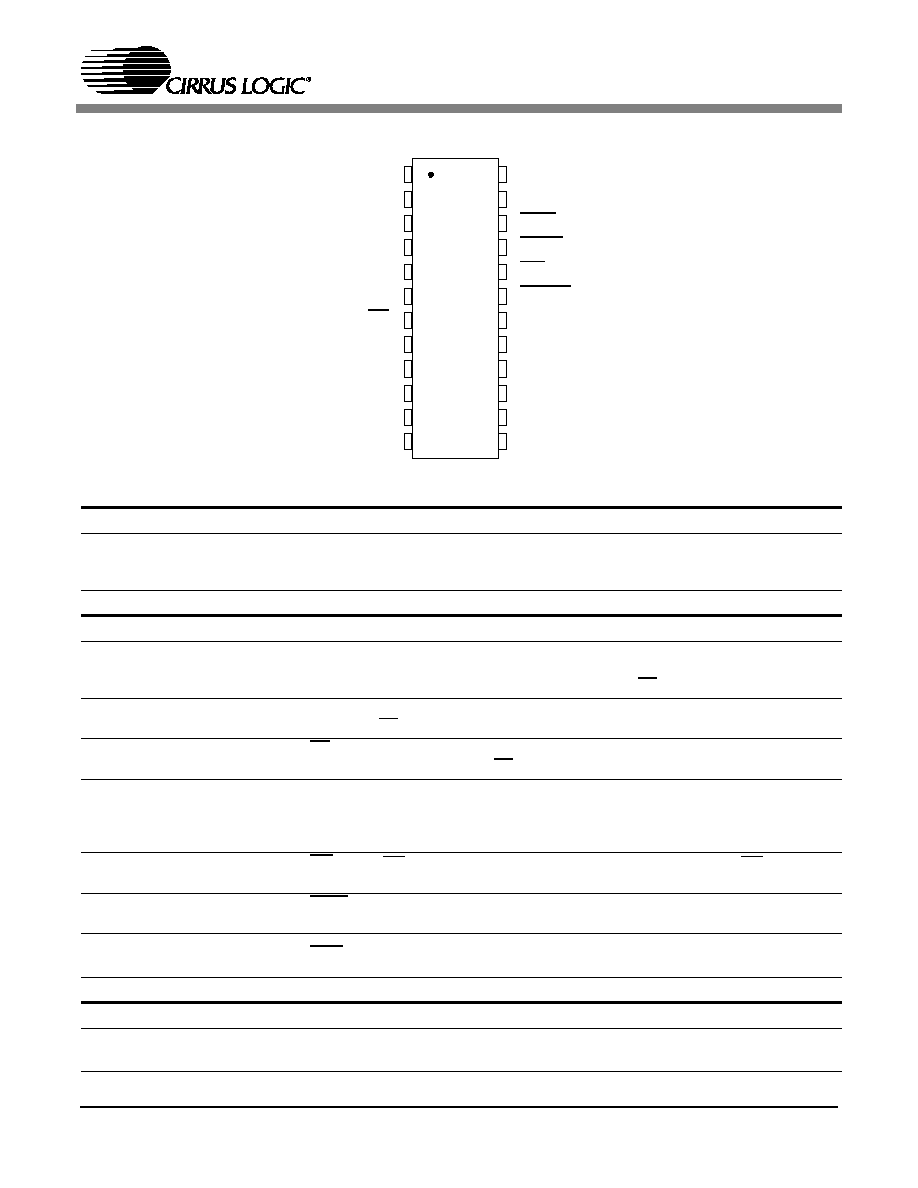
CS5460A
51
6. PIN DESCRIPTION
1
2
3
4
5
6
7
8
17
18
19
20
21
22
23
24
9
10
11
12
13
14
15
16
Crystal Out
XOUT
CPU Clock Output
CPUCLK
Positive Digital Supply
VD+
Digital Ground
DGND
Serial Clock Input
SCLK
Serial Data Output
SDO
Chip Select
CS
Mode Select
MODE
Differential Voltage Input
VIN+
Differential Voltage Input
VIN-
Voltage Reference Output
VREFOUT
Voltage Reference Input
VREFIN
XIN
Crystal In
SDI
Serial Data Input
EDIR
Energy Direction Indicator
EOUT
Energy Output
INT
Interrupt
RESET
Reset
NC
No Connect
PFMON
Power Fail Monitor
I
IN+
Differential Current Input
I
IN-
Differential Current Input
VA+
Positive Analog Supply
VA-
Analog Ground
Clock Generator
Crystal Out
Crystal In
1,24
XOUT, XIN - A gate inside the chip is connected to these pins and can be used with a
crystal to provide the system clock for the device. Alternatively, an external (CMOS
compatible clock) can be supplied into XIN pin to provide the system clock for the device.
CPU Clock Output
2
CPUCLK - Output of on-chip oscillator which can drive one standard CMOS load.
Control Pins and Serial Data I/O
Serial Clock Input
5
SCLK - A clock signal on this pin determines the input and output rate of the data for the
SDI and SDO pins respectively. This input is a Schmitt trigger to allow for slow rise time
signals. The SCLK pin will recognize clocks only when CS is low.
Serial Data Output
6
SDO - SDO is the output pin of the serial data port. Its output will be in a high impedance
state when CS is high.
Chip Select
7
CS - When low, the port will recognize SCLK. An active high on this pin forces the SDO
pin to a high impedance state. CS should be changed when SCLK is low.
Mode Select
8
MODE - When at logic high, the CS5460A can perform the auto-boot sequence with the
aid of an external serial EEPROM to receive commands and settings. When at logic low,
the CS5460A assumes normal "host mode" operation. This pin is pulled down to logic
low if left unconnected, by an internal pull-down resistor to DGND.
Interrupt
20
INT - When INT goes low it signals that an enabled event has occurred. INT is cleared
(logic 1) by writing the appropriate command to the CS5460A.
Energy Output
21
EOUT - The energy output pin output a fixed-width pulse rate output with a rate (pro-
grammable) proportional to real (billable) energy.
Energy Direction
Indicator
22
EDIR - The energy direction indicator indicates if the measured energy is negative.
Serial Data Input
23
SDI - the input pin of the serial data port. Data will be input at a rate determined by SCLK.
Measurement and Reference Input
Differential
Voltage Inputs
9,10
VIN+, VIN- - Differential analog input pins for voltage channel.

CS5460A
52
Voltage
Reference Output
11
VREFOUT - The on-chip voltage reference is output from this pin. The voltage reference
has a nominal magnitude of 2.5 V and is reference to the VA- pin on the converter.
Voltage
Reference Input
12
VREFIN - The voltage input to this pin establishes the voltage reference for the on-chip
modulator.
Differential
Current Inputs
15,16
IIN+, IIN- - Differential analog input pins for current channel.
Power Supply Connections
Positive
Digital Supply
3
VD+ - The positive digital supply is nominally +5 V ±10% relative to DGND.
Digital Ground
4
DGND - The common-mode potential of digital ground must be equal to or above the
common-mode potential of VA-.
Negative
Analog Supply
13
VA- - The negative analog supply pin must be at the lowest potential.
Positive
Analog Supply
14
VA+ - The positive analog supply is nominally +5 V ±10% relative to VA-.
Power Fail Monitor
17
PFMON - The power fail Monitor pin monitors the analog supply. Typical threshold level
(PMLO) is 2.45 V with respect to the VA- pin. If PFMON voltage threshold is tripped, the
LSD (low-supply detect) bit is set in the Status Register. Once the LSD bit has been set,
it will not be able to be reset until the PFMON voltage increases ~100 mV (typical) above
the PMLO voltage. Therefore, there is hysteresis in the PFMON function.
RESET
19
Reset - When reset is taken low, all internal registers are set to their default states.
Other
No Connection
18
NC - No connection. Pin should be left floating.
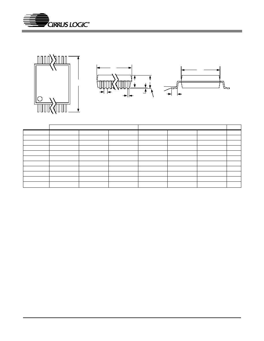
CS5460A
53
7. PACKAGE DIMENSIONS
Notes: 1. "D" and "E1" are reference datums and do not included mold flash or protrusions, but do include mold
mismatch and are measured at the parting line, mold flash or protrusions shall not exceed 0.20 mm per
side.
2. Dimension "b" does not include dambar protrusion/intrusion. Allowable dambar protrusion shall be
0.13 mm total in excess of "b" dimension at maximum material condition. Dambar intrusion shall not
reduce dimension "b" by more than 0.07 mm at least material condition.
3. These dimensions apply to the flat section of the lead between 0.10 and 0.25 mm from lead tips.
INCHES
MILLIMETERS
NOTE
DIM
MIN
NOM
MAX
MIN
NOM
MAX
A
--
--
0.084
--
--
2.13
A1
0.002
0.006
0.010
0.05
0.13
0.25
A2
0.064
0.068
0.074
1.62
1.73
1.88
b
0.009
--
0.015
0.22
--
0.38
2,3
D
0.311
0.323
0.335
7.90
8.20
8.50
1
E
0.291
0.307
0.323
7.40
7.80
8.20
E1
0.197
0.209
0.220
5.00
5.30
5.60
1
e
0.022
0.026
0.030
0.55
0.65
0.75
L
0.025
0.03
0.041
0.63
0.75
1.03
0∞
4∞
8∞
0∞
4∞
8∞
JEDEC #: MO-150
Controlling Dimension is Millimeters.
24L SSOP PACKAGE DRAWING
E
N
1 2 3
e
b
2
A1
A2
A
D
SEATING
PLANE
E1
1
L
SIDE VIEW
END VIEW
TOP VIEW
CS5460A
54
8. ORDERING INFORMATION
CS5460A-BS
24-pin SSOP
-40 to 85 ∞C
CS5460A-BSZ
24-pin SSOP
-40 to 85 ∞C
Lead Free
9. CHANGE HISTORY
Revision
Date
Changes
F2
September 2004
Added Lead Free part numbers
Contacting Cirrus Logic Support
For a complete listing of Direct Sales, Distributor, and Sales Representative contacts, visit the Cirrus Logic web site at:
http://www.cirrus.com/corporate/contacts/sales/cfm
IMPORTANT NOTICE
"Preliminary" product information describes products that are in production, but for which full characterization data is not yet available. "Advance" product infor-
mation describes products that are in development and subject to development changes. Cirrus Logic, Inc. and its subsidiaries ("Cirrus") believe that the infor-
mation contained in this document is accurate and reliable. However, the information is subject to change without notice and is provided "AS IS" without warranty
of any kind (express or implied). Customers are advised to obtain the latest version of relevant information to verify, before placing orders, that information being
relied on is current and complete. All products are sold subject to the terms and conditions of sale supplied at the time of order acknowledgment, including those
pertaining to warranty, patent infringement, and limitation of liability. No responsibility is assumed by Cirrus for the use of this information, including use of this
information as the basis for manufacture or sale of any items, or for infringement of patents or other rights of third parties. This document is the property of Cirrus
and by furnishing this information, Cirrus grants no license, express or implied under any patents, mask work rights, copyrights, trademarks, trade secrets or
other intellectual property rights. Cirrus owns the copyrights associated with the information contained herein and gives consent for copies to be made of the
information only for use within your organization with respect to Cirrus integrated circuits or other parts of Cirrus. This consent does not extend to other copying
such as copying for general distribution, advertising or promotional purposes, or for creating any work for resale.
An export permit needs to be obtained from the competent authorities of the Japanese Government if any of the products or technologies described in this ma-
terial and controlled under the "Foreign Exchange and Foreign Trade Law" is to be exported or taken out of Japan. An export license and/or quota needs to be
obtained from the competent authorities of the Chinese Government if any of the products or technologies described in this material is subject to the PRC Foreign
Trade Law and is to be exported or taken out of the PRC.
CERTAIN APPLICATIONS USING SEMICONDUCTOR PRODUCTS MAY INVOLVE POTENTIAL RISKS OF DEATH, PERSONAL INJURY, OR SEVERE
PROPERTY OR ENVIRONMENTAL DAMAGE ("CRITICAL APPLICATIONS"). CIRRUS PRODUCTS ARE NOT DESIGNED, AUTHORIZED, OR WARRANT-
ED TO BE SUITABLE FOR USE IN LIFE-SUPPORT DEVICES OR SYSTEMS OR OTHER CRITICAL APPLICATIONS. INCLUSION OF CIRRUS PRODUCTS
IN SUCH APPLICATIONS IS UNDERSTOOD TO BE FULLY AT THE CUSTOMER'S RISK.
Cirrus Logic, Cirrus, and the Cirrus Logic logo designs are trademarks of Cirrus Logic, Inc. All other brand and product names in this document may be trade-
marks or service marks of their respective owners. Microwire is a trademark of National Semiconductor Corporation.