Preliminary Product Information
This document contains information for a new product.
Cirrus Logic reserves the right to modify this product without notice.
1
Copyright
©
Cirrus Logic, Inc. 1999
(All Rights Reserved)
P.O. Box 17847, Austin, Texas 78760
(512) 445 7222 FAX: (512) 445 7581
http://www.cirrus.com
CS61318
E1 Line Interface Unit
Features
s
E1 Line Interface Unit
s
No Crystal Needed for Jitter Attenuation
s
Meets CTR-12/TBR-12 Jitter Tolerance and Attenu-
ation Requirements
s
Meets ITU-T G.775 Requirements for LOS and AIS
s
Meets the BS6450 Transmitter Short-Circuit
Requirements for E1 Applications
s
AWG for User Programmable Pulse Shapes
s
Line Quality Monitoring Function
s
TX Driver High Impedance / Low Power Control
s
AIS and LOS Monitoring
s
Generation and Detection of Loop Up / Loop Down
Signaling
s
Selectable HDB3 Encoding/Decoding
s
Selectable Unipolar or Bipolar I/O
s
Compliant with:
-- ITU-T Recommendations: G.703, G.732, G.775, I.431
-- ETSI ETS 300 011, 300 233, CTR 12, TBR 13
-- TR-NET-00499
Description
The CS61318 is an E1 primary rate line interface unit.
This device combines the complete analog transmit and
receive circuitry for a single, full-duplex interface E1
rates. The device provides jitter attenuation compliant to
CTR12/TBR13 without requiring an external crystal. Al-
so, the CS61318 is pin and function compatible with the
Level One LXT318.
In addition to a basic hardware control mode, a host
mode is available that gives the user an enhanced func-
tionality via a serial microprocessor interface. The
extended features include custom pulse shape genera-
tion, AIS and LOS monitoring functions, signal strength
monitoring, and generation and detection of loop up and
loop down codes.
ORDERING INFORMATION
CS61318-IL
28-pin PLCC
CS61318-IP
28-pin PDIP
TCLK
TDATA/TPOS
UBS/TNEG
JASEL
RCLK
RDATA/RPOS
BPV/RNEG
INT/NLOOP
LOS
2
3
4
E
N
C
O
D
E
R
11
REMOTE
LOOPBACK
8
7
6
D
E
C
O
D
E
R
23
12
INBAND
NLOOP
& LOS
PROCESSOR
RECEIVE
CLOCK
GENERATOR
9
10
XTALIN
XTALOUT
5
21
22
14
15
MODE
RV+
RGND TGND
TV+
JITTER
ATTEN
TIMING
& DATA
RECOVERY
LOS/
NLOOP
Clear
REGISTERS & CONTROL LOGIC
TAOS Enable
JITTER
ATTEN
TRANSMIT
TIMING &
CONTROL
PULSE
SHAPING
CIRCUITRY
ROM / RAM
LINE DRIVERS
SERIAL
PORT
LLOOP
Enable
LOCAL
LOOPBACK
(ANALOG)
EQUALIZER
CONTROL
SLICERS
& PEAK
DETECT
NOISE &
CROSSTALK
FILTERS
MAGNITUDE
EQUALIZER
AGC
13
16
28
26
27
24
25
18
19
20
1
TTIP
TRING
CLKE/TAOS
CS/RLOOP
SCLK/LLOOP
SDI/LBO1
SDO/LBO2
LATN
RTIP
RRING
MCLK
LOCAL
LOOPBACK
(DIGITAL)
DS441PP2
AUG `99

CS61318
2
DS441PP2
TABLE OF CONTENTS
1 CHARACTERISTICS AND SPECIFICATIONS ......................................................................... 4
ABSOLUTE MAXIMUM RATINGS ........................................................................................... 4
RECOMMENDED OPERATING CONDITIONS ....................................................................... 4
DIGITAL CHARACTERISTICS ................................................................................................. 4
ANALOG SPECIFICATIONS .................................................................................................... 5
E1 SWITCHING CHARACTERISTICS ..................................................................................... 6
SERIAL PORT SWITCHING CHARACTERISTICS.................................................................. 7
2 THEORY OF OPERATION ........................................................................................................ 8
2.1 Operating Modes ............................................................................................................... 8
2.2 Master Clocks .................................................................................................................... 8
2.3 Transmitter ......................................................................................................................... 8
2.4 Transmit All Ones Select ................................................................................................... 9
2.4.1 Receiver ................................................................................................................ 9
2.4.2 Clock Recovery ..................................................................................................... 9
2.4.3 Jitter Tolerance ..................................................................................................... 9
2.4.4 Receiver Line Attenuation Indication ..................................................................... 9
2.5 Jitter Attenuator ................................................................................................................. 9
2.6 Receiver Loss of Signal ................................................................................................... 10
2.7 Local Loopback ................................................................................................................ 10
2.8 Remote Loopback ............................................................................................................ 11
2.9 Network Loopback ........................................................................................................... 11
2.10 Alarm Indication Signal .................................................................................................. 11
2.11 Serial Interface ............................................................................................................... 11
2.11.1 Control Register 1: Address 0x10 ............................................................................... 13
2.11.2 Control Register 2: Address 0x11 ............................................................................. 14
2.11.3 Equalizer Gain (EQGAIN): Address 0x12 ................................................................... 14
2.11.4 Arbitrary Waveform RAM Address (RAM): Address 0x13 .......................................... 14
2.12 Interrupts ........................................................................................................................ 15
2.13 Power On Reset / Reset ................................................................................................ 15
2.14 Power Supply ................................................................................................................. 15
3 ARBITRARY WAVEFORM GENERATION ............................................................................. 16
4 PIN DESCRIPTION .................................................................................................................. 19
4.1 Power Supplies ................................................................................................................ 20
4.2 Oscillator .......................................................................................................................... 20
4.3 Control ............................................................................................................................. 20
4.4 Status ............................................................................................................................... 21
4.5 Serial Control Interface .................................................................................................... 21
4.6 Data Input/Output ............................................................................................................ 22
5 PACKAGE DIMENSIONS ........................................................................................................ 24
6 APPLICATIONS ....................................................................................................................... 26
Contacting Cirrus Logic Support
For a complete listing of Direct Sales, Distributor, and Sales Representative contacts, visit the Cirrus Logic web site at:
http://www.cirrus.com/corporate/contacts/
Preliminary product information describes products which are in production, but for which full characterization data is not yet available. Advance product infor-
mation describes products which are in development and subject to development changes. Cirrus Logic, Inc. has made best efforts to ensure that the information
contained in this document is accurate and reliable. However, the information is subject to change without notice and is provided "AS IS" without warranty of any
kind (express or implied). No responsibility is assumed by Cirrus Logic, Inc. for the use of this information, nor for infringements of patents or other rights of third
parties. This document is the property of Cirrus Logic, Inc. and implies no license under patents, copyrights, trademarks, or trade secrets. No part of this publi-
cation may be copied, reproduced, stored in a retrieval system, or transmitted, in any form or by any means (electronic, mechanical, photographic, or otherwise)
without the prior written consent of Cirrus Logic, Inc. Items from any Cirrus Logic website or disk may be printed for use by the user. However, no part of the
printout or electronic files may be copied, reproduced, stored in a retrieval system, or transmitted, in any form or by any means (electronic, mechanical, photo-
graphic, or otherwise) without the prior written consent of Cirrus Logic, Inc. Furthermore, no part of this publication may be used as a basis for manufacture or
sale of any items without the prior written consent of Cirrus Logic, Inc. The names of products of Cirrus Logic, Inc. or other vendors and suppliers appearing in
this document may be trademarks or service marks of their respective owners which may be registered in some jurisdictions. A list of Cirrus Logic, Inc. trade-
marks and service marks can be found at http://www.cirrus.com.

CS61318
DS441PP2
3
LIST OF FIGURES
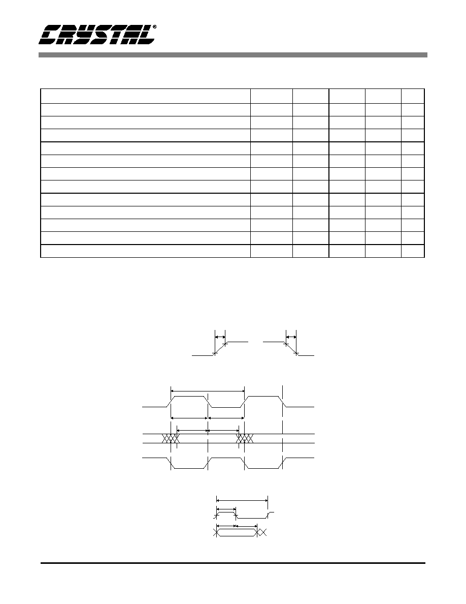
Figure 1. Signal Rise and Fall Characteristics ................................................................. 6
Figure 2. Recovered Clock and Data Switching Characteristics ...................................... 6
Figure 3. Transmit Clock and Data Switching Characteristics ......................................... 6
Figure 4. Serial Port Write Timing Diagram ..................................................................... 7
Figure 5. Serial Port Read Timing Diagram ..................................................................... 7
Figure 6. Mask of the Pulse at the 2048 kbps Interface ................................................... 8
Figure 7. LATN Pulse Width encoding ........................................................................... 10
Figure 8. Typical Jitter Transfer Function ....................................................................... 10
Figure 9. Input/Output Timing (showing address 0x10) ................................................. 12
Figure 10. Phase Definition of Arbitrary Waveform ........................................................ 16
Figure 11. Example of Summing of Waveforms ............................................................. 16
Figure 12. CS61318 Host Mode Operation .................................................................... 26
Figure 13. Hardware Mode Configuration ..................................................................... 27
LIST OF TABLES
Table 1. Data Output/Clock Relationship ........................................................................... 9
Table 2. Register Map..................................................................................................... 12
Table 3. Control Register 1 (0x10) Decoding................................................................... 15
Table 4. CS61318 Diagnostic Mode Availability .............................................................. 17
Table 5. Transformer Specification .................................................................................. 18
Table 6. Recommended Tranformers for the CS61318 ................................................... 18

CS61318
4
DS441PP2
1
CHARACTERISTICS AND SPECIFICATIONS
ABSOLUTE MAXIMUM RATINGS
WARNING: Operation at or beyond these limits may result in
permanent damage to the device. Normal operation is not guaranteed at these extremes.
Notes: 1. Transient currents of up to 100 mA will not cause SCR latch-up. Also TTIP, TRING, TV+ and TGND can
withstand a continuous current of 100 mA.
RECOMMENDED OPERATING CONDITIONS
Notes: 2. TV+ must not exceed RV+ by more than 0.3 V.
3. Power consumption figures assume device is driving line load over operating temperature range. The
consumption of both the IC and the load are included. Digital input levels are within 10% of the supply
rails and digital outputs are driving a 50 pF capacitive load.
4. Typical consumption corresponds to 50% ones density and medium line length at 5.0 V.
5. Maximum consumption corresponds to 100% ones density and maximum line length at 5.25 V.
DIGITAL CHARACTERISTICS
(TA = -40
∞
C to 85
∞
C; TV+, RV+ = 5.0 V
±
5%; GND = 0 V)
Notes: 6. This specification guarantees TTL compatibility (V
OH
= 2.4 V @ I
OUT
= -40
µ
A).
7. Output drivers are TTL compatible and will drive CMOS logic levels into a CMOS load.
Parameter
Symbol
Min
Max
Units
DC Supply
(referenced to RGND=TGND=0 V)
RV+
TV+
-
-
6.0
(RV+) + 0.3
V
V
Input Voltage, Any Pin
V
in
RGND-0.3
(RV+) + 0.3
V
Input Current, Any Pin
(Note 1)
I
in
-10
10
mA
Ambient Operating Temperature
T
A
-40
85
∞
C
Storage Temperature
T
stg
-65
150
∞
C
Parameter
Symbol
Min
Typ
Max
Units
DC Supply
(Note 2) RV+, TV+
4.75
5.0
5.25
V
Ambient Operating Temperature
T
A
-40
25
85
∞
C
Power Consumption, Long Haul
(Notes 3,4,5)
P
C
-
390
630
mW
Power Consumption, Short Haul
(Notes 3,4,5)
P
C
-
480
710
mW
Parameter
Symbol
Min
Typ
Max
Units
High-Level Input Voltage
(Note 6)
PINS 1-4, 24-28
V
IH
2.0
-
-
V
Low-Level Input Voltage
(Note 6)
PINS 1-4, 24-28
V
IL
-
-
0.8
V
High-Level Output Voltage
(Notes 6, 7)
I
OUT
= -40
µ
A
PINS 6-8, 25
V
OH
2.4
-
-
V
Low-Level Output Voltage
(Notes 6, 7)
I
OUT
= 1.6 mA
PINS 6-8, 25
V
OL
-
-
0.4
V
Input Leakage Current
-
-
±
10
µ
A

CS61318
DS441PP2
5
ANALOG SPECIFICATIONS
(TA = -40
∞
C to 85
∞
C; TV+, RV+ = 5.0 V
±
5%; GND = 0 V)
Notes: 8. Using a 0.47 µF capacitor in series with the primary of a transformer recommended in the Applications
Section.
9. Pulse amplitude measured at the secondary of the transformer across a 75
load.
10. Pulse amplitude measured at the secondary of the transformer across a 120
load.
11. Assuming that jitter free clock is input to TCLK.
12. Not production tested. Parameters guaranteed by design and characterization.
13. Measured broadband through a 0.5
resistor across the secondary of the transmitter transformer
during the transmission of an all ones data pattern.
14. Data decision threshold established after the receiver equalizer filters pulse overshoot and undershoot.
15. Jitter tolerance for 0 dB input signal level. Jitter tolerance increases at lower frequencies.
Parameter
Min
Typ
Max
Units
Transmitter
AMI Output Pulse Amplitudes
(Note 8)
E1, 75
(Note 9)
E1, 120
(Note 10)
2.14
2.7
2.37
3.0
2.6
3.3
V
V
Transmitter Output Impedance
Transformer turns ratio = 1:2
Low Z, Long Haul
1.5
Jitter Added by the Transmitter
(Notes 11,12)
10 Hz - 8 kHz
8k Hz - 40 kHz
10 Hz - 40 kHz
Broad Band
-
-
-
-
0.015
0.015
0.015
0.020
-
-
-
-
UI
UI
UI
UI
Positive to Negative Pulse Imbalance
(Notes 8, 12)
-
0.2
0.5
dB
Transmitter Short Circuit Current
(Notes 8, 13)
-
-
50
mA RMS
Receiver
RTIP/RRING Input Impedance
-
20k
-
Sensitivity Below DSX (0 dB = 3.0 V)
-36
48
-
-
-
-
dB
mV
Sensitivity Below G.703 (0 dB = 2.4 V) E1 - Short Haul
-15
430
-
-
-
-
dB
mV
Loss of Signal Threshold
-
-42
-
dB
Data Decision Threshold
(Note 14)
45
50
55
% of peak
Allowable Consecutive Zeros before LOS
160
175
190
bits
Receiver Input Jitter Tolerance - Short Haul
(Note 15)
10 kHz - 100 kHz
(Note 12, 15) 2 kHz
(Note 12, 15) 10 Hz and below
0.35
6.0
300
-
-
-
-
-
-
UI
UI
UI
Receiver Input Jitter Tolerance - Long Haul
10 kHz - 100 kHz
(Note 12, 15) 1 Hz
0.35
138
-
-
-
-
UI
UI
CS61318
6
DS441PP2
E1 SWITCHING CHARACTERISTICS
(TA = -40
∞
C to 85
∞
C; TV+, RV+ = 5.0 V
±
5%;
GND = 0 V; Inputs: Logic 0 = 0 V, Logic 1 = RV+; See Figures 1, 2, & 3)
Notes: 16. MCLK provided by an external source to TCLK.
17. RCLK duty cycle will be 62.5% or 37.5% when jitter attenuator FIFO limits are reached.
18. At max load of 1.6mA and 50pF.
19. Host Mode (CLKE = 1).
20. Host Mode (CLKE = 0).
Parameter
Symbol
Min
Typ
Max
Units
TCLK Frequency
f
tclk
-
2.048
-
MHz
TCLK Duty Cycle
(Note12) t
pwh2
/t
pw2
40
50
60
%
MCLK Frequency
(Note 16)
f
mclk
-
2.048
-
MHz
RCLK Duty Cycle
(Note 17) t
pwh1
/t
pw1
45
50
55
%
Rise Time, All Digital Outputs
(Note 18)
t
r
-
-
85
ns
Fall Time, All Digital Outputs
(Note 19)
t
f
-
-
85
ns
TPOS/TNEG to TCLK Falling Setup Time
t
su2
25
-
-
ns
TCLK Falling to TPOS/TNEG Hold Time
t
h2
25
-
-
ns
RPOS/RNEG Valid Before RCLK Falling
(Note 19)
t
su1
100
194
-
ns
RPOS/RNEG Valid Before RCLK Rising
(Note 20)
t
su1
100
194
-
ns
RPOS/RNEG Valid After RCLK Falling
(Note 19)
t
h1
100
194
-
ns
RPOS/RNEG Valid After RCLK Rising
(Note 20)
t
h1
100
194
-
ns
Any Digital Output
t r
t f
10%
10%
90%
90%
Figure 1. Signal Rise and Fall Characteristics
RCLK
tpw1
tpwl1
tpwh1
(CLKE = 1)
(CLKE = 0)
RCLK
RPOS
RNEG
su1
h1
t
t
Figure 2. Recovered Clock and Data Switching Characteristics
TCLK
TPOS/TNEG
t su2
t h2
t pwh2
t pw2
Figure 3. Transmit Clock and Data Switching Characteristics
CS61318
DS441PP2
7
SERIAL PORT SWITCHING CHARACTERISTICS
(TA = -40
∞
to 85
∞
C; TV+, RV+ = 5V
±
5%;
Inputs: Logic 0 = 0 V, Logic 1 = RV+)
Notes: 21. Output load capacitance = 50 pF
Parameter
Symbol
Min
Typ
Max
Units
SDI to SCLK Setup Time
t
dc
50
-
-
ns
SCLK to SDI Hold Time
t
cdh
50
-
-
ns
SCLK Low Time
t
cl
240
-
-
ns
SCLK High Time
t
ch
240
-
-
ns
SCLK Rise and Fall Time
t
r
, t
f
-
-
50
ns
CS to SCLK Setup Time
t
cc
50
-
-
ns
SCLK to CS Hold Time
t
cch
50
-
-
ns
CS Inactive Time
t
cwh
250
-
-
ns
SCLK to SDO Valid
(Note 21)
t
cdv
-
-
200
ns
CS to SDO High Z
t
cdz
-
100
-
ns
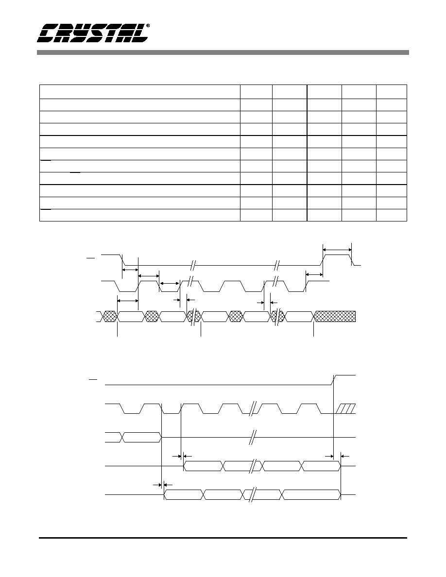
t dc
t cc
LSB
LSB
MSB
CONTROL BYTE
DATA BYTE
CS
SCLK
SDI
t ch
t cwh
t cch
t cdh
t cl
t cdh
Figure 4. Serial Port Write Timing Diagram
HIGH Z
CS
SCLK
SDO
CLKE = 1
SDI
cdv
t
cdv
t
cdz
t
SDO
CLKE = 0
LAST ADDR BIT
D0
D1
D6
D7
D0
D1
D6
D7
Figure 5. Serial Port Read Timing Diagram
CS61318
8
DS441PP2
2 THEORY OF OPERATION
The CS61318 E1 Line Interface is a fully integrated
transceiver designed for 2.048 Mbps E1 operation.
The device provides an interface to twisted pair or
co-axial media through standard pulse transformers
and matching resistors. For added flexibility, the
device can be controlled through a serial micropro-
cessor interface (Host Mode Operation) or via de-
vice pins (Hardware Mode).
2.1
Operating Modes
The CS61318 can be controlled in stand-alone
hardware interface mode (MODE pin is low), or by
a microcontroller in serial host mode (MODE pin is
high). Additional functionality is available in the
host mode as described in the Serial interface sec-
tion.
2.2
Master Clocks
The CS61318 requires a reference clock for the re-
ceiver and the jitter attenuator. A 2.048 MHz exter-
nal clock can be input to MCLK, or a 4x crystal can
be connected to the on-chip oscillator. This fre-
quency reference should be within +50 ppm of the
nominal operating frequency. Jitter and wander on
the reference clock will degrade jitter attenuation
and receiver jitter tolerance. If MCLK is provided,
the crystal oscillator is ignored.
2.3
Transmitter
The transmitter accepts digital E1 input data and
drives appropriately shaped AMI (Alternate Mark
Inversion) pulses onto a transmission line through
a transformer. The transmit data (TPOS & TNEG
or TDATA) is sampled on the falling edge of the
input clock, TCLK.
Tying TNEG high for more than 16 TCLK cycles
enables unipolar I/O mode. This changes TPOS to
TDATA, RPOS to RDATA, and RNEG to BPV. In
this mode the HDB3 encoder and decoder is en-
abled on both the receive and transmit paths.
The CS61318 drives a 75
or 120
line through
the appropriate transformer and matching resistors.
A summary of transformer and resistor configura-
tions is given in the Applications section at the end
of this datasheet. Using the recommended circuits
will produce E1 pulses compliant to the G.703 tem-
plate shown in Figure 6.
Custom transmit pulse shapes may be implemented
by writing pulse shape coefficients to on-board
pulse shape registers. Custom pulses may be used
to correct for pulse shape degradation or distortion
caused by improper termination, suboptimal inter-
connect wiring, or loading from external compo-
nents such as high voltage protection devices. Use
of this feature is described in the Arbitrary Wave-
form Generation section.
The CS61318 will detect the absence of TCLK, and
will force TTIP and TRING to high impedance af-
ter 175 bit periods, preventing transmission when
269 ns
244 ns
194 ns
219 ns
488 ns
Nominal Pulse
0
10
50
80
90
100
110
120
-10
-20
Percent of
nominal
peak
voltage
Figure 6. Mask of the Pulse at the 2048 kbps Interface

CS61318
DS441PP2
9
data input is not present. In host mode, the trans-
mitter can be set to high impedance by setting the
TxHIZ bit, CR2.1, to "1."
When any transmit control bit (TAOS or LLOOP)
is toggled, the transmitter outputs will require ap-
proximately 22 bit periods to stabilize. The trans-
mitter will take longer to stabilize when RLOOP is
selected because the timing circuitry must adjust to
the new frequency.
2.4
Transmit All Ones Select
The transmitter provides for all ones insertion at the
frequency of TCLK. If TCLK is absent, then
MCLK is used (or the quartz crystal generated fre-
quency in the absence of MCLK). Transmit all
ones is selected when TAOS, pin 28, (CR1.7 = 1, in
host mode) goes high, and causes continuous ones
to be transmitted on the line (TTIP and TRING).
When TAOS is active, the TPOS and TNEG
(TDATA) inputs are ignored. If Remote Loopback
is in effect, any TAOS request will be ignored.
2.4.1
Receiver
The receiver extracts data and clock from the input
signal and outputs clock and synchronized data.
The Long Haul receiver can receive signals over
the entire range down to -36dB at E1 rates. The in-
coming pulses are amplified, equalized and filtered
before being fed to the comparator for peak detec-
tion, slicing and data recovery. The clock and data
recovery circuit exceeds the jitter tolerance specifi-
cations of ITU-T G.823 and ETSI CTR12. The
RTIP and RRING inputs are biased to an interme-
diate DC level and treat the input signal differen-
tially.
2.4.2
Clock Recovery
The clock recovery circuit is a third-order phase-
locked loop. The clock and data recovery circuit is
tolerant of long strings of consecutive zeros, and
will successfully receive a 1-in-175, jitter-free in-
put signal.
Data on RPOS and RNEG (RDATA), is stable and
may be latched using the falling edge of recovered
clock, RCLK. In host mode, CLKE, pin 28, deter-
mines the clock polarity for which output data is
stable and valid as shown in Table 1. When CLKE
is high, RPOS and RNEG (RDATA) are valid on
the falling edge of RCLK. When CLKE is low,
RPOS and RNEG are valid on the rising edge of
RCLK.
Table 1. Data Output/Clock Relationship
2.4.3
Jitter Tolerance
The CS61318 has excellent jitter tolerance, accept-
ing as much as 0.35UI of jitter from 10 kHz to
100 kHz without error.
2.4.4
Receiver Line Attenuation Indica-
tion
The LATN pin, pin 18, outputs a coded signal that
represents the signal level at the input of the receiv-
er. As shown in Figure 7, the LATN output is mea-
sured against RCLK to provide the signal level in
7.5 dB increments. In host mode, the receive input
signal level can be read from the Equalizer Gain
register, address 0x12, to greater resolution, divid-
ing the input range into 20 steps of 2 dB incre-
ments.
2.5
Jitter Attenuator
Jitter attenuation can be implemented in either the
transmit (JASEL is low) or receive (JASEL is high)
MODE
(pin 5)
CLKE
(pin 28)
DATA
CLOCK
Clock Edge for
Valid Data
LOW
Don't
Care
RPOS
RNEG
RCLK
Rising
HIGH
LOW
RPOS
RNEG
SDO
RCLK
RCLK
SCLK
Rising
Rising
Falling
HIGH
HIGH
RPOS
RNEG
SDO
RCLK
RCLK
SCLK
Falling
Falling
Rising
CS61318
10
DS441PP2
paths, or it can be eliminated from the circuit by
setting the XTALIN, pin 9, high. The jitter attenu-
ator on the CS61318 does not require a crystal, and
can be activated by setting XTALIN, pin 9, low
(preferred) or by floating pin 9.
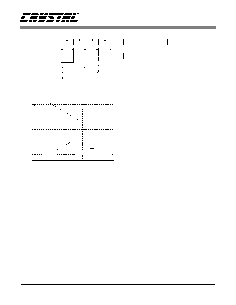
The jitter attenuator's corner frequency is approxi-
mately 1.25 Hz in order to comply with ETSI 300
011, CTR12, and recommendation I.431. A typical
jitter attenuation graph is shown in Figure 8.
2.6
Receiver Loss of Signal
The receiver will indicate loss of signal by setting
LOS, pin 12 high (CR1.0 = 1 in host mode), upon
power up, reset, when receiver gain is maximized,
or upon receiving 175+/-15 consecutive zeros. Re-
ceived zeros are counted based on recovered clock
cycles. When in the LOS state, received data is not
output from RPOS/RNEG (RDATA); but is
squelched until the device comes out of LOS. The
LOS condition is exited using ITU-T G.775 crite-
ria, namely 12.5% ones density for 175+/-75 bit pe-
riods with no more than 100 consecutive zeros. The
receiver recovers signals down to -36 dB, and LOS
will be declared below this signal level.
In LOS, the RCLK frequency depends on whether
MCLK is applied, and whether the jitter attenuator
is in the transmit or receive path. If the jitter atten-
uator is in the receive path, the jitter attenuator will
hold over the average incoming data frequency pri-
or to LOS. RPOS (RDATA) and RNEG pins are
forced low upon LOS.
When the jitter attenuator is in the transmit path or
not used, the clock recovery is referenced to
MCLK, if provided, or the crystal oscillator. The
frequency of RCLK in this case will simply remain
slaved to the clock reference upon loss of data. The
recovered clock remains as a 50% duty cycle clock.
2.7
Local Loopback
Local loopback is selected by setting LLOOP, pin
27, high (CR1.6 = 1 in host mode). Selecting local
loopback causes clock and data presented on
TCLK, TPOS/TNEG (TDATA) to be output at
RCLK, RPOS/RNEG (RDATA). Inputs to the
transmitter are still transmitted on TTIP and
RCLK
LATN
1
2
3
4
5
LATN = 1 RCLK, 9.5 dB of Attenuation
LATN = 2 RCLK, 1 9.5
LATN = 3 RCLK, 28.5 dB of Attenuation
LATN = 4 RCLK, 0 dB of Attenuation
dB of Attenuation
Figure 7. LATN Pulse Width encoding
A
tte
n
uat
ion
i
n
d
B
Frequency in Hz
10
20
30
40
50
60
1
10
100
1 k
10 k
Minimum Attenuation Limit
Measured Performance
0
CS61318
Figure 8. Typical Jitter Transfer Function

CS61318
DS441PP2
11
TRING, unless TAOS has been selected, in which
case AMI-encoded continuous ones are transmitted
at the TCLK frequency. The receiver RTIP and
RRING inputs are ignored when local loopback is
in effect.
2.8
Remote Loopback
Remote loopback is selected by setting RLOOP,
pin 26, high (CR1.5 = 1 in host mode). In remote
loopback, the recovered clock and data input on
RTIP and RRING are sent back out on the line via
TTIP and TRING. Selecting remote loopback over-
rides a TAOS request. The recovered clock and data
from the incoming signal are also sent to RCLK,
RPOS and RNEG (RDATA). Note: simultaneous se-
lection of local and remote loopback modes will cause
a device reset to occur (see Reset).
2.9
Network Loopback
Network Loopback (automatic remote loopback)
can be commanded from the network when the
Network Loopback detect function is enabled. In
Host Mode, Network Loopback (NLOOP) detec-
tion is enabled by writing ones to TAOS, LLOOP,
and RLOOP, then clearing these three bits on a suc-
cessive write cycle. In hardware mode, Network
Loopback can be enabled by tying RLOOP to
RCLK or by setting TAOS, LLOOP, and RLOOP
high for at least 200 ns, and then low. Once enabled
Network Loopback functionality will remain in ef-
fect until RLOOP is activated or the device is reset.
When NLOOP detection is enabled, the receiver
monitors the input data stream for the NLOOP data
patterns (00001 = enable, 001 = disable). When an
NLOOP enable data pattern is repeated for a mini-
mum of five seconds (with less than 10E-3 BER),
the device initiates a remote loopback. Once Net-
work Loopback detection is enabled and activated
by the NLOOP data pattern, the loopback is identi-
cal to Remote Loopback initiated at the device.
NLOOP is reset if the disable pattern (001) is re-
ceived for 5 seconds, or by activation of RLOOP.
NLOOP is temporarily suspended by LLOOP, but
the NLOOP state is not reset.
2.10
Alarm Indication Signal
The receiver sets the register bit, AIS, to "1" when
less than 9 zeros are detected out of 8192 bit peri-
ods. AIS returns to "0" upon the first read after the
AIS condition is removed, determined by 9 or more
zeros out of 8192 bit periods.
2.11
Serial Interface
In the Host Mode, pins 24 through 28 serve as a mi-
crocontroller interface. On-chip registers can be
written to via the SDI pin or read from via the SDO
pin at the clock rate determined by SCLK. Through
these registers, a host controller can be used to con-
trol operational characteristics and monitor device
status. The serial port read/write timing is indepen-
dent of the system transmit and receive timing.
Data transfers are initiated by taking the chip select
input, CS, low (CS must initially be high). Address
and input data bits are clocked in on the rising edge
of SCLK. The clock edge on which output data is
stable and valid is determined by CLKE as shown
in Table 1. Data transfers are terminated by setting
CS high. CS may go high no sooner than 50 ns after
the rising edge of the SCLK cycle corresponding to
the last write bit. For a serial data read, CS may go
high any time to terminate the output and set SDO
to high impedance.
Figure 9 shows the timing relationships for data
transfers when CLKE = 0. When CLKE = 1, data
bit D7 is held until the falling edge of the 16th clock
cycle. When CLKE = 0, data bit D7 is held valid
until the rising edge of the 17th clock cycle. SDO
goes high-impedance after CS goes high or at the
end of the hold period of data bit D7.
SDO goes to a high impedance state when not in
use. SDO and SDI may be tied together in applica-
tions where the host processor has a bi-directional
I/O port.

CS61318
12
DS441PP2
An address/command byte, shown in Figure 9,
points to addresses 0x10 through 0x14 (address
0x10 shown), and precedes a data byte. The first bit
of the address/command byte determines whether a
read or a write is requested. The next six bits con-
tain the address. The last bit is ignored. Data to the
internal registers is input on the eight clock cycles
immediately following the address/command byte.
CS
SCLK
SDO
CLKE = 0
SDI
D6
D5
D4
D3
D2
D1
D0
D7
0
0
D7
D6
D5
D4
D3
D2
D1
D0
Address/Command Byte
Data Input/Output
0
0
0
1
0
R/W
Figure 9. Input/Output Timing (showing address 0x10)
Note: All Control Registers initialize to 0x00.
7
6
5
4
3
2
1
0
ADDR
Control Register 1
TAOS
LLOOP
RLOOP
Reserved
Set to "0"
Reserved
Set to "0"
HDB3
NLOOP
LOS
0x10 R/W
Control Register 2
AIS
RAMPLSE
Reserved
set to `0"
LOOPDN
LOOPUP
RPWDN
TxHIZ
Reserved
set to `0"
0x11 R/W
Equalizer Gain
(EQGAIN)
X
X
X
EQ4
EQ3
EQ2
EQ1
EQ0
0x12 R
Arbitrary Waveform RAM
Address
MSB
-
-
-
-
-
-
LSB
0x13 R/W
Reserved
Set to "0"
0
0
0
0
0
0
0
0
0x14
Table 2. Register Map

CS61318
DS441PP2
13
2.11.1 Control Register 1: Address 0x10
TAOS
Transmit All Ones Select
When TAOS = 1, all ones are transmitted at the TCLK frequency
LLOOP
Local Loopback
When LLOOP = 1, data input at TPOS, TNEG (TDATA) is internally looped back and output on
RPOS, RNEG (RDATA). TCLK is routed to RCLK, through the jitter attenuator, if activated.
RLOOP
Remote Loopback
When RLOOP = 1, clock and data recovered by the receiver are sent back through the transmit
path and retransmitted. The clock and data are routed through the jitter attenuator, if activated.
BITS 4:3
Reserved - Set Bits 3 & 4 to "0" for proper operation.
HDB3
Setting HDB3 to "1" enables HDB3 encoding and decoding.
NLOOP
Network Loopback
NLOOP = 1 when a network loopback code has been detected on the received signal.
An interrupt will occur when NLOOP changes state unless a "1" is written to NLOOP disabling
the interrupt.
LOS
Loss Of Signal
LOS = 1 when the loss of signal criteria have been met (See Receiver Loss of Signal).
LOS = 0 when a valid signal is being received.
Writing a "1" to LOS disables interrupts due to LOS and the LOS Change indication in bits 5
and 6.
7 (MSB)
6
5
4
3
2
1
0 (LSB)
TAOS
LLOOP
RLOOP
Reserved
Set to "0"
Reserved
Set to "0"
HDB3
NLOOP
LOS

CS61318
14
DS441PP2
2.11.2 Control Register 2: Address 0x11
AIS
Alarm Indication Signal.
AIS = 1 when an all ones pattern is present at the receiver. This bit is reset to "0" by the first
read occurring after the AIS condition has cleared.
An interrupt will occur when AIS is present unless a "1" is written to AIS disabling the interrupt.
RAMPLSE
When RAMPLSE = 1, output pulse shapes are determined by the codes in the internal, pro-
grammable, transmit RAM.
RSVD
Reserved
Set to "0" for proper operation.
LOOPDN
Loop Down
In Long Haul mode, setting LOOPDN to "1" causes the data pattern 001... to be repetitively
transmitted.
LOOPUP
Loop Up
In Long Haul mode, setting LOOPUP to "1" causes the data pattern 00001... to be repetitively
transmitted.
RPWDN
Receiver Power Down
When RPWDN = 1, the receiver circuitry is powered down, but the transmitter is still active.
TxHIZ
Transmitter High Impedance
When TxHIZ = 1 the transmitter goes to a low-power, high-impedance state
2.11.3 Equalizer Gain (EQGAIN): Address 0x12
EQ[4:0]
The receive equalizer gain settings are broken down into 20 segments and provided at the five
LSBs of this register, EQ4 - EQ0. 00001 corresponds to -2 dB, 10100 corresponds to -40 dB.
The three MSBs are don't cares.
2.11.4 Arbitrary Waveform RAM Address (RAM): Address 0x13
RAM[7:0]
Arbitrary Waveform RAM;
Onboard RAM is provided so that custom pulse shapes may be downloaded (see Arbitrary
Waveform Generation section). Writing the waveform RAM requires first writing the Ad-
dress/Command Byte with the write bit set (see Figure 10) followed by a data byte which spec-
ifies the RAM address to be written. Following these two bytes is a third byte that represents
the waveform coefficient to be stored in the target address. There are 42 RAM byte locations
(numbered h00 to h29).
7 (MSB)
6
5
4
3
2
1
0 (LSB)
AIS
RAMPLSE
RSVD
LOOPDN
LOOPUP
RPWDN
TxHIZ
RSVD
7 (MSB)
6
5
4
3
2
1
0 (LSB)
X
X
X
EQ4
EQ3
EQ2
EQ1
EQ0
7 (MSB)
6
5
4
3
2
1
0 (LSB)
RAM.7
RAM.6
RAM.5
RAM.4
RAM.3
RAM.2
RAM.1
RAM.0

CS61318
DS441PP2
15
Reading the control/status registers returns their
current status or setting. Control Register 1 (0x10))
outputs the status of NLOOP and LOS. Additional-
ly, 5, 6, and 7 encoded as shown in Tables 3.
2.12
Interrupts
An interrupt will occur (INT pulls low) in response
to a change in the LOS, AIS or NLOOP bits. The
interrupt is cleared when the host processor writes
a "1" to the respective bit in the control register.
Writing a "1" to LOS or NLOOP over the serial in-
terface has three effects:
1)
The current interrupt on the serial interface
will be cleared. (Note that simply reading the
register bits will not clear the interrupt).
2)
Output data bits 5, 6 and 7 will be reset as ap-
propriate.
3)
Interrupts for the corresponding LOS and
NLOOP will be prevented from occurring.
Writing a "0" to either LOS or NLOOP enables the
corresponding interrupt for LOS and NLOOP.
2.13
Power On Reset / Reset
Upon power-up, the IC is held in a static state until
the supply crosses a threshold of approximately
3 Volts. When this threshold is crossed, the device
will delay for about 10 ms to allow the power sup-
ply to reach operating voltage. After this delay, cal-
ibration of the transmit and receive sections
commences. Because power up conditions can vary
considerably, it is recommended that the device be
reset after the power supply has stabilized to ensure
a known initial operational condition.
The internal frequency generators can be calibrated
only if a reference clock is present. The reference
clock for the transmitter is provided by TCLK. The
reference for the receiver is either the crystal oscil-
lator or MCLK. If both the oscillator and MCLK
are active, MCLK will be used as the reference
source. The initial calibration should take less than
20 ms after pulses are input to the receiver.
In operation, the device is continuously calibrated,
making the performance of the device independent
of power supply or temperature variations. The
continuous calibration function forgoes any re-
quirement to reset the line interface when in opera-
tion. However, a reset function is available which
will reinitiate calibration and clear all registers and
clear the Network Loopback function.
In Host Mode, a reset is initiated by simultaneously
writing RLOOP and LLOOP to the register. The re-
set will set all registers to "0" and initiate a calibra-
tion. A reset will also set LOS high in the Short
Haul configuration.
In Hardware Mode, the CS61318 is reset by simul-
taneously setting RLOOP and LLOOP high for at
least 200 ns. Hardware reset will clear Network
Loopback functionality
2.14
Power Supply
The device operates from a single +5 Volt supply.
Separate pins for transmit and receive supplies pro-
vide internal isolation. These pins should be decou-
Table 3. Control Register 1 (0x10) Decoding
Bits
Status Mode
7
6
5
0
0
0 Reset has occurred, or no program input
0
0
1 RLOOP active
0
1
0 LLOOP active
0
1
1 LOS has changed state since last Clear
LOS occurred
1
0
0 TAOS active
1
0
1 NLOOP has changed state since last
Clear NLOOP occurred
1
1
0 TAOS and LLOOP active
1
1
1 LOS and NLOOP have both changed
state since last Clear NLOOP and Clear
LOS

CS61318
16
DS441PP2
pled to their respective grounds. TV+ must not
exceed RV+ by more than 0.3 V.
Decoupling and filtering of the power supplies is
crucial for the proper operation of the analog cir-
cuits in both the transmit and receive paths. A 47
µ
F
tantalum and 1.0
µ
F mylar or ceramic capacitor
should be connected between TV+ and TGND, and
a 0.1
µ
F mylar or ceramic capacitor should be con-
nected between RV+ and RGND. Place capacitors
as closely as possible to their respective power sup-
ply pins. Wire-wrap breadboarding of the line in-
terface is not recommended because lead resistance
and inductance serve to defeat the function of the
decoupling capacitors.
3 ARBITRARY WAVEFORM
GENERATION
In addition to the predefined pulse shapes, the user
can create custom pulse shapes under the Host
Mode operation. This flexibility allows the board
designer to accommodate non-standard cables,
EMI filters, protection circuitry, etc.
The arbitrary pulse shape of mark (a transmitted
"1") is specified by describing it's pulse shape
across three Unit Intervals (UIs). This allows, for
example, the long-haul return-to-zero tail to extend
into the next UI, or two UIs, as is required for iso-
lated pulses.
Each UI is divided into multiple phases, and the us-
ers defines the amplitude of each phase. The wave-
form of a space (a transmitted "0") is fixed at zero
volts. Examples of the phases are shown in
Figure 10. In all cases, to define an arbitrary wave-
form, the user writes to the Waveform Register ei-
ther 36, 39 or 42 times (12, 13 or 14 phases per UI
for three UIs). The phases are written in the order:
UI1/phase1, UI1/phase2, ... , UI1/phase14,
UI2/phase1, ... , UI2/phase14, UI3/phase1, ... ,
UI3/phase14.
The CS61318 divides the 488 ns UI into 14 uni-
form phases (34.9 ns each), and uses the phase in-
formation written for all 14 phases of each UI.
When transmitting pulses, the CS61318 will add
the amplitude information from the prior two sym-
bols with the amplitude of the first UI of the current
symbol before outputting a signal on TTIP/TRING.
Therefore, a mark preceded by two spaces will be
output exactly as the mark is programmed. Howev-
er, when one mark is preceded by marks, the first
portion of the last mark may be modified. With
AMI data, where successive pulses have opposite
polarity, the undershoot tail of one pulse will cause
the rising edge of the next mark to rise more quick-
ly, as shown in Figure 11.
E1 Arbitrary Waveform Example
Figure 10. Phase Definition of Arbitrary Waveform
Figure 11. Example of Summing of Waveforms

CS61318
DS441PP2
17
The amplitude of each phase is described by a 7-bit,
2's compliment number, where a positive value de-
scribes pulse amplitude, and a negative value de-
scribes pulse undershoot. The positive full value is
hex 3F. The negative full value is hex 40. For E1
shielded twisted pair, the typical output voltage is
27 mV/LSB. All voltages are peak voltages across
the TTIP and TRING outputs.
Using the circuits given in the Applications section
of the data sheet, the output impedance of the de-
vice will be approximately equal to the impedance
of the line. This means that the voltage on the trans-
former secondary will be twice the values stated
above. Note that although the full scale digital in-
put is 3F, it is recommended that full scale output
voltage on the transformer primary be limited to
2.4 Vpk. At higher output voltages, the driver may
not drive the requested output voltage.
The amplitude information for all phases is written
via the serial-port to Arbitrary Waveform RAM
registers (see Arbitrary Waveform RAM register
for description). Each phase amplitude is written as
an eight-bit byte, where the first phase of the sym-
bol is written first.
The contents of the Arbitrary Waveform RAM can
be verified by performing a read operation. Read-
ing the waveform RAM requires first writing the
Address/Command Byte with the R/W bit set to
"1" (see Figure 10) followed by a data byte which
specifies the RAM address to be read. On subse-
quent SCLK's the contents of the specified RAM
location will be clocked out on SDO.
Notes: 1. In Hardware Mode the Diagnostic Modes are selected by directly setting the pins on the device; in Host
Mode, the appropriate register bits are written for Diagnostic Modes.
2. In Host Mode the interrupts can be masked by writing a "1" to the LOS bit; there is no masking in the
Hardware Mode.
Diagnostic Mode
Availability (Note 1)
H/W Host
Host Mode (Note 2)
Maskable
Loopback Modes
Local Loopback (LLOOP)
Yes
Yes
No
Remote Loopback (RLOOP)
Yes
Yes
No
In-band Network Loopback (NLOOP)
Yes
Yes
Yes
Internal Data Pattern Generation and Detection
Transmit All Ones (TAOS)
Yes
Yes
No
In-band Loop-up/down Code Generator
No
Yes
No
Error Detection
Bipolar Violation Detection (BPV)
Yes
Yes
No
Alarm Condition Monitoring
Receive Loss of Signal Monitoring (LOS)
Yes
Yes
Yes
Receive Alarm Indication Signal Monitoring (AIS)
No
Yes
Yes
Other Diagnostic Reports
Receive Line Attenuation Indicator (LATN)
Yes
Yes
No
Table 4. CS61318 Diagnostic Mode Availability

CS61318
18
DS441PP2
Turns ratio: 120
Twisted Pair Application
1:2 step-up transmit, 1:1 receive
Turns ratio: 75
Twisted Pair Application
1:1.58 step-up transmit, 1:1 receive
Table 5. Transformer Specification
Turns
Ratio(s)
Manufacturer
Part Number
Package Type
1:1CT
Pulse Engineering
PE-64936
1.5 kV, through-hole, single
Valor
PT5008
Schott
67130840
Valor
ST5085
1.5 kV, surface mount, single
Schott
31187
1:2CT
Pulse Engineering
PE-65351
1.5 kV, through-hole, single
Valor
PT5004
Schott
617130850
Valor
ST5086
1.5 kV, surface mount, single
Schott
31188
1:1CT
1:2CT
Pulse Engineering
PE-68678
1.5 kV, surface mount, dual
Valor
ST5162
Pulse Engineering
PE-68877
1.5 kV, surface mount, dual
extended temp.
Pulse Engineering
T-1068
1.5 kV, surface mount, quad port
Valor
ST5173
Pulse Engineering
T-1031
3 kV, surface mount, dual
1:1.58 CT
Pulse Engineering
T-1229
1.5 kV, through hole, single
Table 6. Recommended Tranformers for the CS61318
CS61318
DS441PP2
19
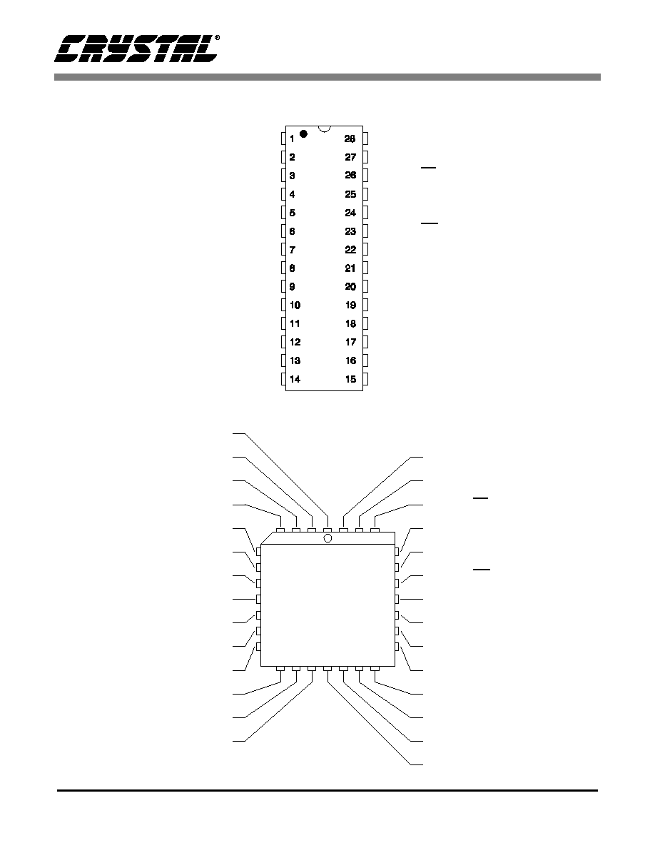
4 PIN DESCRIPTION
MCLK
TAOS/CLKE
TCLK
LLOOP/SCLK
TPOS/TDATA
RLOOP/CS
TNEG/UBS
SDO
MODE
SDI
RNEG/BPV
NLOOP/INT
RPOS/RDATA
RGND
RCLK
RV+
XTALIN
RRING
XTALOUT
RTIP
JASEL
LATN
LOS
NC
TTIP
TRING
TGND
TV+
top
view
22
20
24
19
21
23
25
3
27
2
4
26
28
1
12
14
16
18
13
15
17
8
6
10
5
7
9
11
MCLK
TCLK
TAOS/CLKE
TPOS/TDATA
LLOOP/SCLK
TNEG/UBS
RLOOP/CS
MODE
SDO
RNEG/BPV
SDI
RPOS/RDATA
NLOOP/INT
RCLK
RGND
XTALIN
RV+
XTALOUT
RRING
JASEL
RTIP
LOS
LATN
TTIP
NC
TGND
TRING
TV+

CS61318
20
DS441PP2
4.1
Power Supplies
TV+ - Power Supply, Transmit Driver, Pin 15.
Power supply for the transmit driver; typically +5 Volts.
TGND - Ground Transmit Driver, Pin 14.
Power supply ground for the transmit driver; typically 0 Volts.
RV+ - Power Supply, Pin 21.
Power supply for all subcircuits except the transmit driver; typically +5 Volts.
RGND - Ground, Pin 22.
Power supply ground for all subcircuits except the transmit driver; typically 0 Volts.
4.2
Oscillator
XTALIN, XTALOUT - Crystal Connections, Pins 9 and 10.
A 8.192 MHz crystal can be connected across these pins. This oscillator provides the reference
frequency for the LIU if MCLK is not provided. The load capacitance presented to the crystal by these
pins should be approximately 19pF (IC and package, when soldered into a circuit board). The jitter
attenuator may be disabled by tying pin 9 to RV+ through a 1k
resistor, and floating XTALOUT. When
pin 9 has no clock input, a clock must be supplied to the MCLK pin. Alternatively an external 8.192 MHz
clock can be driven into pin 9, and the jitter attenuator circuit will operate.
If MCLK is provided, and XTALIN is tied low or floated, the jitter attenuator will be enabled.
4.3
Control
MCLK - Master Clock Input, Pin 1.
Either MCLK or the crystal oscillator provide the master frequency reference for the CS61318. If both
MCLK and the crystal oscillator are present, the oscillator is ignored. MCLK should be 2.048 MHz for E1
operation. In a Loss of Signal state, RCLK will be derived from MCLK, through the jitter attenuator, if
active. If MCLK is not provided, the jitter attenuator will hold the RCLK frequency in a Loss of Signal
state. MCLK should be grounded if it is not used.
MODE - Mode Select Input, Pin 5.
Setting the MODE pin high puts the CS61318 into Host Mode where the device is controlled by a
microprocessor, via a serial port. Setting the MODE pin low, configures the part for hardware mode
control where control and status are provided through dedicated pins. The MODE pin is internally pulled
down placing the part in Hardware Mode when this pin is left floating. Tying the MODE pin to RCLK
places the chip in Hardware Mode and enables the HDB3 encoder/decoder (provided that coder mode
has been enabled; see the description for TNEG/UBS pin).
TAOS - Transmit All Ones Select Input, Pin 28 (Hardware Mode).
Setting TAOS to logic 1 causes continuous ones to be transmitted at the TCLK frequency. When TAOS
is high, TPOS and TNEG (TDATA) are not output at the TTIP/TRING pins. TAOS is overridden by
Remote Loopback. Setting TAOS, LLOOP, and RLOOP high simultaneously enables Network Loopback
detection.

CS61318
DS441PP2
21
LLOOP - Local Loopback Input, Pin 27(Hardware Mode).
Setting LLOOP to a logic 1 internally routes the transmitter input to the receiver output. If TAOS is low,
the signal being output from the transmitter will be internally routed to the receiver inputs allowing nearly
the entire chip to be tested. If TAOS and LLOOP are set high at the same time, the local loopback will
occur at the jitter attenuator (excluding the transmit and receive circuitry) and the transmitter will
transmit all ones. Simultaneously setting RLOOP and LLOOP high while TAOS is low resets the
CS61318. Simultaneously setting RLOOP, LLOOP and TAOS high enables Network Loopback detection.
RLOOP - Remote Loopback Input, Pin 26 (Hardware Mode).
Setting RLOOP to a logic 1 causes the received signal to be passed through the jitter attenuator (if
active) and retransmitted onto the line. The internal encoders/decoders will be bypassed in Remote
Loopback. Simultaneously setting RLOOP and LLOOP high while TAOS is low resets the CS61318.
Simultaneously setting RLOOP, LLOOP and TAOS high enables Network Loopback detection.
JASEL - Jitter Attenuator Select, Pin 11.
If the jitter attenuator is enabled (crystal oscillator active, or XTALIN tied low or floated with MCLK
provided), setting JASEL high places the jitter attenuator in the receive path; setting JASEL low places
the jitter attenuator in the transmit path.
NC - No Connect, Pin 17.
The input voltage to this pin does not effect normal operation.
4.4
Status
LOS - Loss Of Signal Output, Pin 12.
LOS goes high when 175 consecutive zeros are received. LOS returns low when the ones density
reaches 12.5% (based on 175 consecutive bit periods, starting with a one and containing less than 100
consecutive zeros, as prescribed in ITU-T G.775). If LOS is true, and the jitter attenuator is in the
receive path, RCLK will smoothly transition to MCLK if provided; RCLK will retain the frequency prior to
LOS if MCLK is grounded. If the jitter attenuator is NOT in the receive path, RCLK will become the
reference clock frequency (MCLK) if provided, or the crystal oscillator.
NLOOP - Network Loopback Output, Pin 23 (Hardware Mode).
NLOOP goes high when a 00001 pattern is received for five seconds putting the CS61318 into network
(remote) loopback. NLOOP is deactivated upon receipt of a 001 pattern for five seconds, or by selection
of LLOOP or RLOOP.
LATN - Line Attenuation Indication Output, Pin 18.
LATN is an encoded output that indicates the receive equalizer gain setting in relation to a five RCLK
cycle period. If LATN is high for one RCLK cycle, the equalizer is set for 9.5 dB gain, two cycles =
19.5 dB gain, three cycles = 28.5 dB gain, four cycles = 0 dB. LATN may be sampled on the rising edge
of RCLK.
4.5
Serial Control Interface
INT - Interrupt Output, Pin 23 (Host Mode).
INT pulls low to flag the host processor when NLOOP, AIS or LOS changes state. INT is an open drain
output and should be tied to the supply through a resistor.

CS61318
22
DS441PP2
SDI - Serial Data Input, Pin 24 (Host Mode).
Data input to the on-chip register is sampled on the rising edge of SCLK. Note: this pin should be tied
to GND during Hardware Mode.
SDO - Serial Data Output, Pin 25 (Host Mode).
Status and control information are output from the on-chip register on SDO. If CLKE is high, SDO is
valid on the rising edge of SCLK. If CLKE is low, SDO is valid on the falling edge of SCLK. SDO goes
to a high-impedance state when the serial port is being written to, or after bit D7 is output or CS goes
high (whichever occurs first). Note: this pin should be tied to GND during Hardware Mode.
CS - Chip Select, Pin 26 (Host Mode).
The serial interface is accessible when CS transitions from high to low.
SCLK - Serial Clock Input, Pin 27 (Host Mode).
SCLK is used to write or read data bits to or from the serial port registers.
CLKE - Clock Edge, Pin 28 (Host Mode).
Setting CLKE to logic 1 causes RPOS and RNEG (RDATA) to be valid on the falling edge of RCLK, and
SDO to be valid on the rising edge of SCLK. Conversely, setting CLKE to logic 0 causes RPOS and
RNEG (RDATA) to be valid on the rising edge of RCLK and SDO to be valid on the falling edge of
SCLK.
4.6
Data Input/Output
TCLK - Transmit Clock Input, Pin 2.
The 2.048 MHz transmit clock is input on this pin. TPOS and TNEG or TDATA are sampled on the
falling edge of TCLK.
TPOS/TNEG - Transmit Positive Pulse, Transmit Negative Pulse, Pins 3 and 4.
Data input to TPOS and TNEG is sampled on the falling edge of TCLK and transmitted onto the line at
TTIP and TRING. An input on TPOS results in transmission of a positive pulse; an input on TNEG
results in transmission of a negative pulse. If TNEG, pin 4, is held high for 16 TCLK cycles, the
CS61318 reconfigures for unipolar (single pin NRZ) data input at pin 3, TDATA. If pin 4 goes low the
CS61318 switches back to two-pin bipolar data input format.
TDATA - Transmit Data, Pin 3.
When pin 4, TNEG/UBS, is held high, pin 3 becomes TDATA, a single-line NRZ (unipolar) data input
sampled on the falling edge of TCLK.
UBS - Unipolar / Bipolar Select, Pin 4.
When UBS is held high for 16 consecutive TCLK cycles (15 consecutive bipolar violations) the CS61318
reconfigures for unipolar (single-line NRZ) data input / output format. Pin 3 becomes TDATA, pin 7
becomes RDATA, and pin 6 becomes BPV.
RCLK - Recovered Clock Output, Pin 8.
RCLK outputs the clock recovered from the input signal at RTIP and RRING. In a Loss of Signal state
RCLK reverts to the MCLK frequency, or retains the frequency prior to the LOS state, depending on the
clocks provided. See the LOS pin description.

CS61318
DS441PP2
23
RNEG/RPOS - Receive Negative Pulse, Receive Positive Pulse, Pins 6 and 7.
Recovered data output on RPOS and RNEG is stable and valid on the rising edge of RCLK in Hardware
Mode. In Host Mode, CLKE determines the edge of RCLK on which RPOS and RNEG are valid. A
positive pulse on RTIP with respect to RRING generates a logic 1 on RPOS; a positive pulse on RRING
with respect to RTIP generates a logic 1 on RNEG.
RDATA - Received Data, Pin 7.
Unipolar data (single-line NRZ) data is output on RDATA when pin 4, TNEG/UBS, is held high.
BPV - Bipolar Violation, Pin 6.
When pin 4 is held high, received bipolar violations are flagged by BPV (RNEG) going high along with
the offending bit output from RDATA. If the HDB3 encoder/decoder is activated, BPV will not flag bipolar
violations resulting from valid zero substitutions.
RTIP,RRING - Receive Tip; Receive Ring, Pins 19,20.
The HDB3 signal received from the line is input via these pins. A 1:1 transformer and appropriate
matching resistors are required as shown in the applications section. Data and clock recovered from the
signal input on these pins is output via RPOS, RNEG, and RCLK.
TTIP, TRING - Transmit Tip; Transmit Ring, Pins 13,16
These pins are the output of the differential transmit driver. The transformer and matching resistors can
be chosen to give the desired pulse height (see Application Schematics).

CS61318
24
DS441PP2
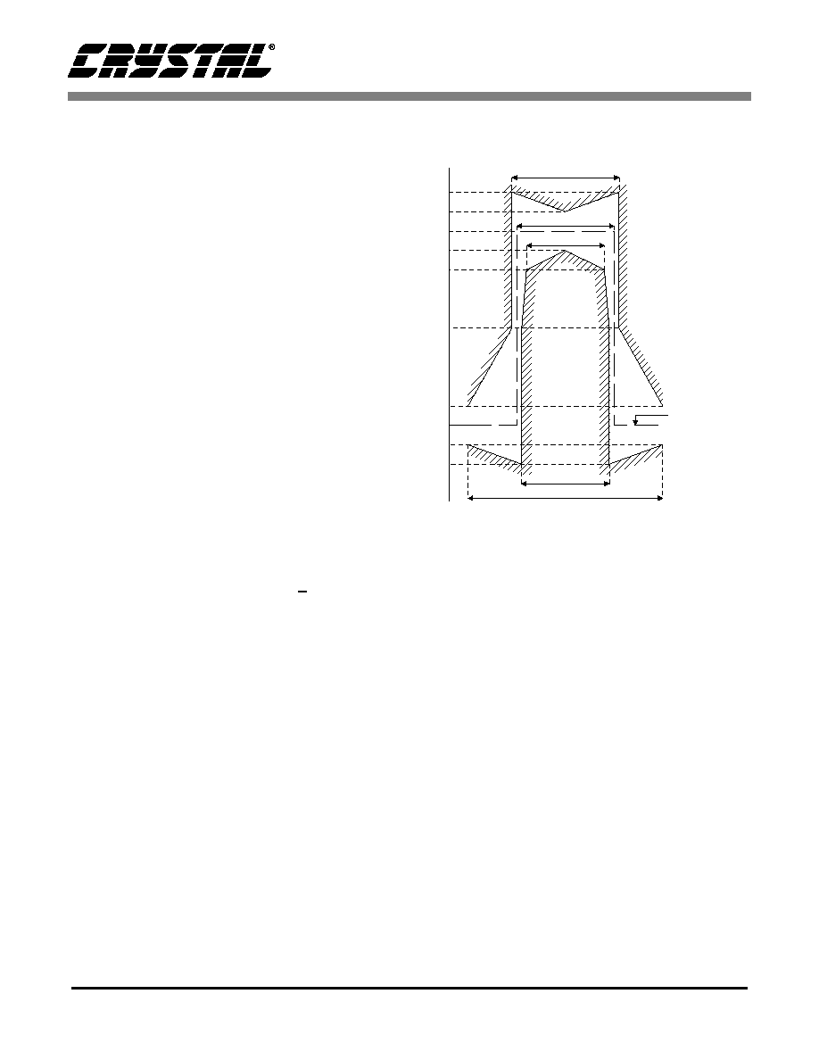
5 PACKAGE DIMENSIONS
1. Positional tolerance of leads shall be within 0.25 mm (0.010 in.) at maximum material condition, in
relation to seating plane and each other.
2. Dimension eA to center of leads when formed parallel.
3. Dimension E does not include mold flash.
INCHES
MILLIMETERS
DIM
MIN
MAX
MIN
MAX
A
0.155
0.200
3.94
5.08
A1
0.020
0.040
0.51
1.02
b
0.014
0.022
0.36
0.56
b1
0.040
0.065
1.02
1.65
c
0.008
0.015
0.20
0.38
D
1.435
1.465
36.45
36.83
E
0.540
0.560
13.72
14.22
e
0.095
0.105
2.41
2.67
eA
0.600
0.625
15.24
15.87
L
0.125
0.150
3.18
3.81
0∞
15∞
0∞
15∞
28 PIN PLASTIC (PDIP) PACKAGE DRAWING
E
D
SEATING
PLANE
b1
e
b
A
L
A1
TOP VIEW
BOTTOM VIEW
SIDE VIEW
1
eA
c
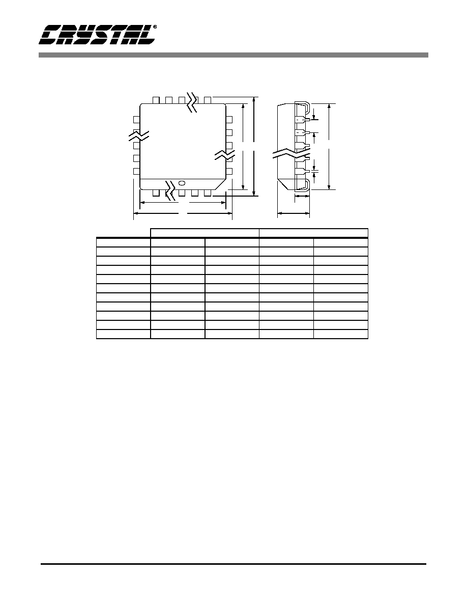
CS61318
DS441PP2
25
INCHES
MILLIMETERS
DIM
MIN
MAX
MIN
MAX
A
0.165
0.180
4.043
4.572
A1
0.090
0.120
2.205
3.048
B
0.013
0.021
0.319
0.533
D
0.485
0.495
11.883
12.573
D1
0.450
0.456
11.025
11.582
D2
0.390
0.430
9.555
10.922
E
0.485
0.495
11.883
12.573
E1
0.450
0.456
11.025
11.582
E2
0.390
0.430
9.555
10.922
e
0.040
0.060
0.980
1.524
JEDEC #: MS-018
28L PLCC PACKAGE DRAWING
D1
D
E1 E
D2/E2
B
e
A1
A

CS61318
26
DS441PP2
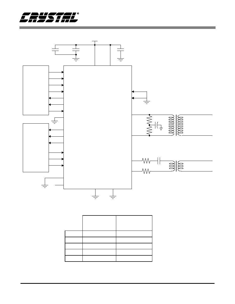
6
APPLICATIONS
Control
&
Monitor
Frame
Format
Encoder/
Decoder
CS61318
IN
HOST
MODE
RECEIVE
LINE
28
1
12
6
5
7
6
8
3
4
2
9
10
RV+
+
33
µ
F
RGND
0.1
µ
F
+5V
21
15
+
1.0
µ
F
TGND
RV+
TV+
CLKE
MCLK
LOS
BPV
MODE
RPOS
RNEG
RCLK
TPOS
TNEG
TCLK
XTALIN
XTALOUT
RGND
TGND
22
14
SCLK
CS
INT
SDI
SDO
RTIP
RRING
TRING
TTIP
19
20
R1
R2
1
5
2
6
T1 1:1
µ
P
Serial
Port
27
26
23
24
25
18
LATN
1 k
11
JASEL
0.47
µ
F
T2 1:N
TRANSMIT
LINE
16
13
0.47
µ
F
2
6
1
5
R3
R4
Figure 12. CS61318 Host Mode Operation
NOTE: The 0.47
µ
F capacitor between R1 & R2 may be omitted if common mode noise is not an issue.
NOTE: The optional 0.47
µ
F DC blocking cap eliminates DC saturation current through T2
E1
75
Coaxial Cable
E1
120
Twisted Pair
R1 (
)
37.5
60
R2 (
)
37.5
60
R3 (
)
15
15
R4 (
)
15
15
T2
1:1.58
1:2
CS61318
DS441PP2
27
Control
&
Monitor
Frame
Format
Encoder/
Decoder
CS61318
IN
HARDWARE
MODE
28
1
26
27
5
7
6
8
3
4
2
9
10
+
33
µ
F
RGND
0.1
µ
F
+5V
21
15
+
1.0
µ
F
TGND
RV+
TV+
TAOS
MCLK
RLOOP
LLOOP
MODE
RPOS
RNEG
RCLK
TPOS
TNEG
TCLK
XTALIN
XTALOUT
RGND
TGND
22
14
RTIP
RRING
TRING
TTIP
24
25
12
23
LOS
NLOOP
11
JASEL
RECEIVE
LINE
19
20
R1
R2
1
5
2
6
T1 1:1
0.47
µ
F
TRANSMIT
LINE
16
13
0.47
µ
F
2
6
1
5
R3
R4
SD I
SDO
T2 1:N
Figure 13. Hardware Mode Configuration
NOTE: The 0.47
µ
F capacitor between R1 & R2 may be omitted if common mode noise is not an issue.
NOTE: The optional 0.47
µ
F DC blocking cap eliminates DC saturation current through T2
E1
75
Coaxial Cable
E1
120
Twisted Pair
R1 (
)
37.5
60
R2 (
)
37.5
60
R3 (
)
15
15
R4 (
)
15
15
T2
1:1.58
1:2