
Features
∑
Provides Analog PCM Line Interface
for T1 and E1 Applications
∑
Provides Line Driver, and Data and
Clock Recovery Functions
∑
Transmit Side Jitter Attenuation
Starting at 6 Hz, with > 300 UI of Jitter
Tolerance
∑
Low Power Consumption
(typically 175 mW)
∑
B8ZS/HDB3/AMI Encoders/Decoders
∑
14 dB of Transmitter Return Loss
∑
Compatible with SONET, M13 , CCITT
G.742, and Other Asynchronous
Muxes
General Description
The CS61535A combines the complete analog transmit
and receive line interface for T1 or E1 applications in a
low power, 28-pin device operating from a +5V supply.
The device features a transmitter jitter attenuator mak-
ing it ideal for use in asynchronous multiplexor systems
with gapped transmit clocks. The CS61535A provides a
matched, constant impedance output stage to insure
signal quality on mismatched, poorly terminated lines.
Both ICs use a digital Delay-Locked-Loop clock and
data recovery circuit which is continuously calibrated
from a crystal reference to provide excellent stability
and jitter tolerance.
Applications
∑
Interfacing network transmission equipment such as
SONET multiplexor and M13 to a DSX-1 cross connect.
∑
Interfacing customer premises equipment to a CSU.
∑
Interfacing to E1 links.
Ordering Information
CS61535A-IP1
28 Pin Plastic DIP
CS61535A-IL1
28 Pin PLCC (j-leads)
MAY '96
DS40F2
1
Crystal Semiconductor Corporation
P.O. Box 17847, Austin, TX 78760
(512) 445-7222 FAX: (512) 445-7581
SIGNAL
QUALITY
MONITOR
13
TTIP
TCLK
7
RRING
RTIP
19
20
17
11
18
TRING
16
TGND
14
CONTROL
DRIVER
MONITOR
LINE RECEIVER
LINE DRIVER
15
PULSE
SHAPER
3
2
6
4
RCLK
8
ACLKI
27
LLOOP
(SCLK)
26
RLOOP
(CS)
25
24
(INT)
LEN0
(SDI)
LEN1
(SDO)
LEN2
28
23
(CLKE)
TAOS
5
MODE
AMI,
B8ZS,
HDB3
CODER
TPOS
[TDATA]
RPOS
[RDATA]
RNEG
[BPV]
TNEG
[TCODE]
MTIP
[RCODE]
MRING
[PCS]
DPM
[AIS]
LOS
12
21
RV+
22
RGND
1
CLOCK &
DATA
RECOVERY
XTALIN
9
XTALOUT
10
JITTER
ATTENUATOR
LOOP
BACK
TV+
[ ] = Pin Function in Extended Hardware Mode
( ) = Pin Function in Host Mode
Copyright
©
Crystal Semiconductor Corporation 1996
(All Rights Reserved)
CS61535A
T1/E1 Line Interface

ABSOLUTE MAXIMUM RATINGS
Parameter
Symbol
Min
Max
Units
DC Supply
(referenced to RGND,TGND=0V)
RV+
TV+
-
-
6.0
(RV+) + 0.3
V
V
Input Voltage, Any Pin
(Note 1)
V
in
RGND-0.3
(RV+) + 0.3
V
Input Current, Any Pin
(Note 2)
I
in
-10
10
mA
Ambient Operating Temperature
T
A
-40
85
∞
C
Storage Temperature
T
stg
-65
150
∞
C
WARNING:Operations at or beyond these limits may result in permanent damage to the device.
Normal operation is not guaranteed at these extremes.
Notes:
1. Excluding RTIP, RRING, which must stay within -6V to (RV+) + 0.3V.
2. Transient currents of up to 100 mA will not cause SCR latch-up. Also TTIP, TRING, TV+ and TGND
can withstand a continuous current of 100 mA.
RECOMMENDED OPERATING CONDITIONS
Parameter
Symbol
Min
Typ
Max
Units
DC Supply
(Note 3) RV+, TV+
4.75
5.0
5.25
V
Ambient Operating Temperature
T
A
-40
25
85
∞
C
Power Consumption
(Notes 4, 5)
P
C
-
290
350
mW
Power Consumption
(Notes 4, 6)
P
C
-
175
-
mW
Notes:
3. TV+ must not exceed RV+ by more than 0.3V.
4. Power consumption while driving line load over operating temperature range. Includes IC and load.
Digital input levels are within 10% of the supply rails and digital outputs are driving a 50 pF load.
5. Assumes 100% ones density and maximum line length at 5.25V.
6. Assumes 50% ones density and 300ft. line length at 5.0V.
CS61535A
2
DS40F2

DIGITAL CHARACTERISTICS
(TA = -40
∞
C to 85
∞
C; TV+, RV+ = 5.0V
±
5%; GND = 0V)
Parameter
Symbol
Min
Typ
Max
Units
High-Level Input Voltage
Pins 1-4, 17, 18, 23-28
(Notes 7, 8, 9)
V
IH
2.0
-
-
V
Low-Level Input Voltage
Pins 1-4, 17, 18, 23-28
(Notes 7, 8, 9)
V
IL
-
-
0.8
V
High-Level Output Voltage (IOUT = -40
µ
A)
Pins 6-8, 11, 12, 25
(Notes 7, 8, 10)
V
OH
4.0
-
-
V
Low-Level Output Voltage (IOUT = 1.6 mA)
Pins 6-8, 11, 12, 23, 25
(Notes 7, 8, 10)
V
OL
-
-
0.4
V
Input Leakage Current (Except Pin 5)
-
-
±
10
µ
A
Low-Level Input Voltage, Pin 5
V
IL
-
-
0.2
V
High-Level Input Voltage, Pin 5
V
IH
(RV+) - 0.2
-
-
V
Mid-Level Input Voltage, Pin 5
(Note 11)
V
IM
2.3
-
2.7
V
Notes:
7. This specification guarantees TTL compatibility (V
OH
= 2.4V @ I
OUT
= -40
µ
A).
8. In Host Mode, pin 23 is an open drain output and pin 25 is a tristate output.
9. Pins 17 and 18 of the CS61535A are digital inputs in the Extended Hardware Mode.
10. Output drivers will drive CMOS logic levels into a CMOS load.
11. As an alternative to supplying a 2.3-to-2.7V input, this pin may be left floating.
ANALOG SPECIFICATIONS
(TA = -40
∞
C to 85
∞
C; TV+, RV+ = 5.0V
±
5%; GND = 0V)
Parameter
Min
Typ
Max
Units
Jitter Attenuator
Jitter Attenuation Curve Corner Frequency
(Note 12)
-
6
-
Hz
T1 Jitter Attenuation in Remote Loopback
(Note 13)
Jitter Freq. [Hz]
Amplitude [UIpp]
10
10
100
10
500
10
1k
5
10k, 40k
0.3
3.0
20
35
40
40
6.0
30
35
50
50
-
-
-
-
-
dB
dB
dB
dB
dB
E1 Jitter Attenuation in Remote Loopback
(Note 14)
Jitter Freq. [Hz]
Amplitude [UIpp]
10
1.5
100
1.5
400
1.5
1k
1.5
10k, 100k
0.2
3.0
20
30
35
35
6.0
32
43
50
50
-
-
-
-
-
dB
dB
dB
dB
dB
Attenuator Input Jitter Tolerance
(Note 15)
12
23
-
UI
Notes: 12. Not production tested. Parameters guaranteed by design and characterization.
13. Attenuation measured at the demodulator output of an HP3785B with input jitter equal to 3/4 of
measured jitter tolerance using a measurement bandwidth of 1 Hz (10<f<100Hz), 4Hz (100<f<1000
Hz) and 10 Hz (f> 1kHz) centered around the jitter frequency. With a 2
15
-1 PRBS data pattern.
Crystal must meet specifcations in CXT6176/8192 datasheet.
14. Jitter measured at the demodulator output of an HP3785A using a measurement
bandwidth not to exceed 20 Hz centered around the jitter frequency. With a 2
15
-1 PRBS data pattern.
Crystal must meet specifications in CXT6176/8192 datasheet.
15. Output jitter increases significantly when attenuator input jitter tolerance is exceeded.
CS61535A
DS40F2
3

ANALOG SPECIFICATIONS
(TA = -40
∞
C to 85
∞
C; TV+, RV+ = 5.0V
±
5%; GND = 0V)
Parameter
Min
Typ
Max
Units
Transmitter
AMI Output Pulse Amplitudes
(Note 16)
E1, 75
(Note 17)
E1, 120
(Note 18)
T1, FCC Part 68
(Note 19)
T1, DSX-1
(Note 20)
2.14
2.7
2.7
2.4
2.37
3.0
3.0
3.0
2.6
3.3
3.3
3.6
V
V
V
V
E1 Zero (space) level (LEN2/1/0 = 0/0/0)
75
application
(Note 17)
120
application
(Note 18)
-0.237
-0.3
-
-
0.237
0.3
V
V
Recommended Output Load at TTIP and TRING
-
75
-
Jitter Added During Remote Loopback
(Note 21)
10Hz - 8kHz
8kHz - 40kHz
10Hz - 40kHz
Broad Band
-
-
-
-
0.005
0.008
0.010
0.015
0.02
0.025
0.025
0.05
UI
UI
UI
UI
Power in 2kHz band about 772kHz
(Notes 12, 16)
12.6
15
17.9
dBm
Power in 2kHz band about 1.544MHz
(Notes 12, 16)
(referenced to power in 2kHz band at 772kHz)
-29
-38
-
dB
Positive to Negative Pulse Imbalance
(Notes 12, 16)
T1, DSX-1
E1 amplitude at center of pulse
E1 pulse width at 50% of nominal amplitude
-
-5
-5
0.2
-
-
0.5
5
5
dB
%
%
Transmitter Return Loss
(Notes 12, 16, 22)
51 kHz to 102 kHz
102 kHz to 2.048 MHz
2.048 MHz to 3.072 MHz
8
14
10
-
-
-
-
-
-
dB
dB
dB
Transmitter Short Circuit Current
(Notes 12, 23)
-
-
50
mA RMS
Notes: 16. Using a 0.47
µ
F capacitor in series with the primary of a transformer recommended
in the Applications Section.
17. Amplitude measured at the transformer (CS61535A-1:1 or 1:1.26) output across a
75
load for line length setting LEN2/1/0 = 0/0/0.
18. Amplitude measured at the transformer (CS61535A-1:1.26) output across a
120
load for line length setting LEN2/1/0 = 0/0/0.
19. Amplitude measured at the transformer (CS61535A-1:1.15) output across a
100
load for line length setting LEN2/1/0 = 0/1/0.
20. Amplitude measured across a 100
load at the DSX-1 cross-connect for line length settings
LEN2/1/0 = 0/1/1, 1/0/0, 1/0/1, 1/1/0 and 1/1/1 after the length of #22 AWG ABAM equivalent cable
specified in Table 3. The CS61535A requires a 1:1.15 transformer.
21. Input signal to RTIP/RRING is jitter free. Values will reduce slightly if jitter free clock is input to TCLK.
22. Return loss = 20 log
10
ABS((z
1
+z
0
)/(z
1
-z
0
)) where z
1
= impedance of the transmitter, and
z
0
= impedance of line load. Measured with a repeating 1010 data pattern with LEN2/1/0 = 0/0/0
and a 1:1 transformer terminated with a 75
load, or a 1:1.26 transformer terminated with a
120
load.
23. Measured broadband through a 0.5
resistor across the secondary of a 1:1.26 transformer
during the transmission of an all ones data pattern for LEN2/1/0 = 0/0/0.
CS61535A
4
DS40F2

ANALOG SPECIFICATIONS
(TA = -40
∞
C to 85
∞
C; TV+, RV+ = 5.0V
±
5%; GND = 0V)
Parameter
Min
Typ
Max
Units
Driver Performance Monitor
MTIP/MRING Sensitivity:
Differential Voltage Required for Detection
-
0.60
-
V
Receiver
RTIP/RRING Input Impedance
-
50k
-
Sensitivity Below DSX (0dB = 2.4V)
-13.6
-
-
dB
Data Decision Threshold
T1, DSX-1
(Note 24)
T1, DSX-1
(Note 25)
T1, FCC Part 68 and E1
(Note 26)
60
53
45
65
65
50
70
77
55
% of peak
% of peak
% of peak
Data Decision Threshold
T1
E1
-
-
65
50
-
-
% of peak
% of peak
Allowable Consecutive Zeros before LOS
160
175
190
bits
Receiver Input Jitter Tolerance
(Note 27)
10kHz - 100kHz
2kHz
10Hz and below
0.4
6.0
300
-
-
-
-
-
-
UI
UI
UI
Loss of Signal Threshold
(Note 28)
0.25
0.30
0.50
V
Notes: 24. For input amplitude of 1.2 V
pk
to 4.14 V
pk
.
25. For input amplitude of 0.5 V
pk
to 1.2 V
pk
and from 4.14 V
pk
to RV+.
26. For input amplitude of 1.05 V
pk
to 3.3 V
pk
.
27. Jitter tolerance increases at lower frequencies. See Figure 11.
28. LOS goes high after 160 to 190 consecutive zeros are received. A zero is output on RPOS and
RNEG (or RDATA) for each bit period where the input signal amplitude remains below the data
decision threshold. The analog input squelch circuit operates when the input signal amplitude above
ground on the RTIP and RRING pins falls within the squelch range long enough for the internal
slicing threshold to decay within this range. Operation of the squelch causes zeros to be output on
RPOS and RNEG as long as the input amplitude remains below 0.25V. During receive LOS, pulses
greater than 0.25V in amplitude may be output on RPOS and RNEG. LOS returns low after the ones
density reaches 12.5% (based upon 175 bit periods starting with a one and containing
less than 100 consecutive zeros) as prescribed in ANSI T1.231-1993.
CS61535A
DS40F2
5
T1 SWITCHING CHARACTERISTICS
(TA = -40
∞
C to 85
∞
C; TV+, RV+ = 5.0V
±
5%;
GND = 0V; Inputs: Logic 0 = 0V, Logic 1 = RV+; See Figures 1, 2, & 3)
Parameter
Symbol
Min
Typ
Max
Units
Crystal Frequency
(Note 29)
f
c
-
6.176000
-
MHz
ACLKI Duty Cycle
t
pwh3
/t
pw3
40
-
60
%
ACLKI Frequency
(Note 30)
f
aclki
-
1.544
-
MHz
RCLK Duty Cycle
(Notes 31, 32)
t
pwh1
/t
pw1
-
-
78
29
-
-
%
%
RCLK Cycle Width
(Note 32)
t
pw1
t
pwh1
t
pwl1
320
130
100
648
190
458
980
240
850
ns
ns
ns
Rise Time, All Digital Outputs
(Note 33)
t
r
-
-
85
ns
Fall Time, All Digital Outputs
(Note 33)
t
f
-
-
85
ns
TPOS/TNEG (TDATA) to TCLK Falling Setup Time
t
su2
25
-
-
ns
TCLK Falling to TPOS/TNEG (TDATA) Hold Time
t
h2
25
-
-
ns
RPOS/RNEG Valid Before RCLK Falling
(Note 34)
t
su1
150
274
-
ns
RDATA Valid Before RCLK Falling
(Note 35)
t
su1
150
274
-
ns
RPOS/RNEG Valid Before RCLK Rising
(Note 31)
t
su1
150
274
-
ns
RPOS/RNEG Valid After RCLK Falling
(Note 34)
t
h1
150
274
-
ns
RDATA Valid After RCLK Falling
(Note 35)
t
h1
150
274
-
ns
RPOS/RNEG Valid After RCLK Rising
(Note 31)
t
h1
150
274
-
ns
TCLK Frequency
f
tclk
-
1.544
-
MHz
TCLK Pulse Width
(Notes 12, 31, 34, 36, 37)
(Notes 35, 36, 37)
t
pwh2
80
150
-
-
500
500
ns
ns
Notes: 29. Crystal must meet specifications described in CXT6176/CXT8192 data sheet.
30. ACLKI provided by an external source or TCLK, but
not RCLK.
31. Hardware Mode, or Host Mode (CLKE = 0).
32. RCLK cycle width will vary with extent by which pulses displaced by jitter. Specified under worst case
jitter conditions: 0.4 UI AMI data displacement for T1 and 0.2 UI AMI data displacement for E1.
33. At max load of 1.6 mA and 50 pF.
34. Host Mode (CLKE = 1).
35. Extended Hardware Mode.
36. The maximum TCLK burst rate is 5 MHz and t
pw2
(min) = 200 ns. The maximum gap size that can
be tolerated on TCLK is 12 VI.
37. The transmitted pulse width does not depend on the TCLK duty cycle.
RCLK
tpw1
tpwl1
tpwh1
HOST MODE
(CLKE = 1)
EXTENDED
HARDWARE
MODE OR
HARDWARE
HOST MODE
(CLKE = 0)
MODE OR
RCLK
RPOS
RNEG
su1
h1
t
t
RDATA
BPV
Figure 1. Recovered Clock and Data Switching Characteristics
CS61535A
6
DS40F2

E1 SWITCHING CHARACTERISTICS
(TA = -40
∞
C to 85
∞
C; TV+, RV+ = 5.0V
±
5%;
GND = 0V; Inputs: Logic 0 = 0V, Logic 1 = RV+; See Figures 1, 2, & 3)
Parameter
Symbol
Min
Typ
Max
Units
Crystal Frequency
(Note 29)
f
c
-
8.192000
-
MHz
ACLKI Duty Cycle
t
pwh3
/t
pw3
40
-
60
%
ACLKI Frequency
(Note 30)
f
aclki
-
2.048
-
MHz
RCLK Duty Cycle
(Notes 31, 32)
t
pwh1
/t
pw1
-
29
-
%
RCLK Cycle Width
(Note 32)
t
pw1
t
pwh1
t
pwl1
310
90
120
488
140
348
670
190
500
ns
ns
ns
RCLK Cycle Width
(Note 32)
t
pw1
t
pwh1
t
pwl1
320
-
100
488
348
140
670
-
-
ns
ns
ns
Rise Time, All Digital Outputs
(Note 33)
t
r
-
-
85
ns
Fall Time, All Digital Outputs
(Note 33)
t
f
-
-
85
ns
TPOS/TNEG (TDATA) to TCLK Falling Setup Time
t
su2
25
-
-
ns
TCLK Falling to TPOS/TNEG (TDATA) Hold Time
t
h2
25
-
-
ns
RPOS/RNEG Valid Before RCLK Falling
(Note 34)
t
su1
100
194
-
ns
RDATA Valid Before RCLK Falling
(Note 35)
t
su1
100
194
-
ns
RPOS/RNEG Valid Before RCLK Rising
(Note 31)
t
su1
100
194
-
ns
RPOS/RNEG Valid After RCLK Falling
(Note 34)
t
h1
100
194
-
ns
RDATA Valid After RCLK Falling
(Note 35)
t
h1
100
194
-
ns
RPOS/RNEG Valid After RCLK Rising
(Note 31)
t
h1
100
194
-
ns
TCLK Frequency
f
tclk
-
2.048
-
MHz
TCLK Pulse Width
(Notes 31, 34, 36, 37)
(Notes 35, 36, 37)
t
pwh2
80
150
-
-
340
340
ns
ns
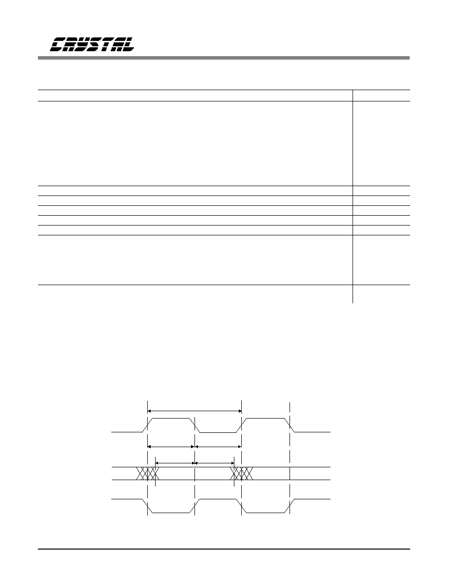
TCLK
TPOS/TNEG
t su2
t h2
t pwh2
t pw2
Figure 3a. Transmit Clock and Data Switching
Characteristics
ACLKI
t pwh3
t pw3
Figure 3b. Alternate External Clock Characteristics
Any Digital Output
t r
t f
10%
10%
90%
90%
Figure 2. Signal Rise and Fall Characteristics
CS61535A
DS40F2
7

SWITCHING CHARACTERISTICS
(TA = -40
∞
to 85
∞
C; TV+, RV+ =
±
5%;
Inputs: Logic 0 = 0V, Logic 1 = RV+)
Parameter
Symbol
Min
Typ
Max
Units
SDI to SCLK Setup Time
t
dc
50
-
-
ns
SCLK to SDI Hold Time
t
cdh
50
-
-
ns
SCLK Low Time
t
cl
240
-
-
ns
SCLK High Time
t
ch
240
-
-
ns
SCLK Rise and Fall Time
t
r
, t
f
-
-
50
ns
CS to SCLK Setup Time
t
cc
50
-
-
ns
SCLK to CS Hold Time
(Note 38)
t
cch
50
-
-
ns
CS Inactive Time
t
cwh
250
-
-
ns
SCLK to SDO Valid
(Note 39)
t
cdv
-
-
200
ns
CS to SDO High Z
t
cdz
-
100
-
ns
Input Valid To PCS Falling Setup Time
t
su4
50
-
-
ns
PCS Rising to Input Invalid Hold Time
t
h4
50
-
-
ns
PCS Active Low Time
t
pcsl
250
-
-
ns
Notes: 38. For CLKE = 0, CS must remain low at least 50 ns after the 16
th
falling edge of SCLK.
39. Output load capacitance = 50pF.
t dc
t cc
LSB
LSB
MSB
CONTROL BYTE
DATA BYTE
CS
SCLK
SDI
t ch
t cwh
t cch
t cdh
t cl
t cdh
Figure 4. Serial Port Write Timing Diagram
CS61535A
8
DS40F2

HIGH Z
CS
SCLK
SDO
CLKE = 1
t cdz
cdv
t
Figure 5. Serial Port Read Timing Diagram
PCS
VALID INPUT DATA
LEN0/1/2, TAOS,
RLOOP, LLOOP,
th4
tsu4
tpcsl
RCODE, TCODE
Figure 6. Extended Hardware Mode Parallel Chip Select Timing Diagram
CS61535A
DS40F2
9

THEORY OF OPERATION
Enhancements in CS61535A
The CS61535A provides higher performance and
more features than the CS61535 including:
∑
50% lower power consumption,
∑
Internally matched transmitter output imped-
ance for improved signal quality,
∑
Optional AMI, B8ZS, HDB3 encoder/decoder
or external line coding support,
∑
Receiver AIS (unframed all ones) detection,
∑
ANSI T1.231-1993 compliant receiver Loss
of Signal (LOS) handling,
∑
Transmitter TTIP and TRING outputs are
forced low when TCLK is static,
∑
The Driver Performance Monitor operates
over a wider range of input signal levels.
∑
Elimination of the requirement that a refer-
ence clock be input on the ACLKI pin.
Existing designs using the CS61535 can be converted
to the higher performance, pin-compatible CS61535A
if the transmit transformer is replaced by a pin-com-
patible transformer with a new turns ratio and the 4.4
resistor used in E1 75
applications is shorted.
Introduction to Operating Modes
The CS61535A supports three operating modes
which are selected by the level of the MODE pin
as shown in Tables 1 and 2, Figure 7, and Figures
A1-A3 of the Applications section.
The CS61535A modes are Hardware Mode, Ex-
tended Hardware Mode, and Host Mode. In
Hardware and Extended Hardware Modes, discrete
pins are used to configure and monitor the device.
The Extended Hardware Mode provides a parallel
chip select input which latches the control inputs
allowing individual ICs to be configured using a
common set of control lines. In the Host Mode, an
external processor monitors and configures the de-
vice through a serial interface. There are thirteen
multi-function pins whose functionality is deter-
mined by the operating mode (see Table 2).
Transmitter
The transmitter takes data from a T1 (or E1) ter-
minal, attenuates jitter, and produces pulses of
appropriate shape. The transmit clock, TCLK,
and transmit data, TPOS & TNEG or TDATA, are
supplied synchronously. Data is sampled on the
falling edge of the input clock, TCLK.
Either T1 (DSX-1 or Network Interface) or E1
G.703 pulse shapes may be selected. Pulse shap-
ing and signal level are determined by "line
length select" inputs as shown in Table 3. The
MODE
HARDWARE
EXTENDED
HARDWARE
HOST
MODE-PIN
INPUT LEVEL
<0.2V
FLOAT, or
2.5V
>(RV+) - 0.2V
CONTROL
METHOD
INDIVIDUAL
CONTROL
LINES
INDIVIDUAL
CONTROL
LINES &
PARALLEL
CHIP
SELECT
SERIAL
µ
-PROCESSOR
PORT
LINE CODE
ENCODER &
DECODER
NONE
AMI,
B8ZS,
HDB3
NONE
AIS DETECTION
NO
YES
NO
DRIVER
PERFORM-
ANCE MONITOR
YES
NO
YES
Table 1. Differences in Operating Modes
MODE
FUNCTION
PIN
HARDWARE
EXTENDED
HARDWARE
HOST
TRANSMITTER
3
TPOS
TDATA
TPOS
4
TNEG
TCODE
TNEG
RECEIVER/DPM
6
RNEG
BPV
RNEG
7
RPOS
RDATA
RPOS
11
DPM
AIS
DPM
17
MTIP
RCODE
MTIP
18
MRING
-
MRING
CONTROL
18
-
PCS
-
23
LEN0
LEN0
INT
24
LEN1
LEN1
SDI
25
LEN2
LEN2
SDO
26
RLOOP
RLOOP
CS
27
LLOOP
LLOOP
SCLK
28
TAOS
TAOS
CLKE
Table 2. Pin Definitions
CS61535A
10
DS40F2

TPOS
TNEG
RNEG
RPOS
TRANSMIT
TRANSFORMER
RRING
RECEIVE
TRANSFORMER
CONTROL
CS62180B
FRAMER
CIRCUIT
TTIP
TDATA
RDATA
TRING
LINE DRIVER
AMI
B8ZS,
HDB3,
CODER
TRANSMIT
TRANSFORMER
RLOOP
PCS
LEN0/1/2
LLOOP
TAOS
CONTROL
HARDWARE MODE
EXTENDED HARDWARE MODE
HOST MODE
CONTROL
5
µ
P SERIAL PORT
RCODE
TCODE
CLKE
BPV
AIS
JITTER
ATTENUATOR
DRIVER MONITOR
LINE DRIVER
LINE RECEIVER
MTIP
MRING
DPM
RTIP
TTIP
TRING
HIGH
SPEED
MUX
(e.g., M13)
CS61535A
CS61535A
TTIP
TPOS
TNEG
RNEG
TRING
RPOS
RRING
RTIP
RLOOP
LEN0/1/2
LLOOP
TAOS
CONTROL
DPM
DRIVER MONITOR
LINE DRIVER
LINE RECEIVER
MTIP
MRING
CS61535A
CS62180B
FRAMER
CIRCUIT
TRANSMIT
TRANSFORMER
RECEIVE
TRANSFORMER
RECEIVE
TRANSFORMER
RRING
RTIP
AIS
DETECT
JITTER
ATTENUATOR
LINE RECEIVER
JITTER
ATTENUATOR
Figure 7. Overview of Operating Modes
CS61535A
DS40F2
11

CS61535A line driver is designed to drive a 75
equivalent load.
For T1 DSX-1 applications, line lengths from 0 to
655 feet (as measured from the transmitter to the
DSX-1 cross connect) are selectable. The five
partition arrangement meets ANSI T1.102-1993
requirements when using ABAM cable. A typical
output pulse is shown in Figure 8. These pulse
settings can also be used to meet CCITT pulse
shape requirements for 1.544 MHz operation.
For T1 Network Interface applications, additional
options are provided. Note that the optimal pulse
width for Part 68 (324 ns) is narrower than the
optimal pulse width for DSX-1 (350 ns). The
CS61535A automatically adjusts the pulse width
based upon the "line length " selection made.
The E1 G.703 pulse shape is supported with line
length selection LEN2/1/0=0/0/0. The pulse
width will meet the G.703 pulse shape template
shown in Figure 9, and specified in Table 4.
For E1 applications, the CS61535A driver pro-
vides 14 dB of return loss during the transmission
of both marks and spaces. This improves signal
quality by minimizing reflections off the trans-
mitter. Similar levels of return loss are provided
for T1 applications.
The CS61535A transmitter will detect a failed
TCLK, and will force the TTIP and TRING out-
puts low.
500
1.0
0.5
0
-0.5
0
250
750
1000
NORMALIZED
AMPLITUDE
AT&T CB 119
SPECIFICATION
CS61535A
PULSE SHAPE
OUTPUT
TIME (nanoseconds)
Figure 8. Typical Pulse Shape at DSX-1 Cross Connect
LEN2
LEN1
LEN0
OPTION SELECTED
APPLICATION
0
1
1
0-133 FEET
DSX-1
ABAM
(AT&T 600B
or 600C)
1
0
0
133-266 FEET
1
0
1
266-399 FEET
1
1
0
399-533 FEET
1
1
1
533-655 FEET
0
0
1
AT&T CB113
(CS61535A only)
REPEATER
0
0
0
CCITT G.703
2.048 MHz E1
0
1
0
FCC Part 68, Option A
CSU NETWORK
INTERFACE
0
1
1
ANSI T1.403
Table 3. Line Length Selection
F or c o axi al cab le ,
75
l oa d a nd
transformer specified
in Application Section.
For shielded twisted
pair, 120
load and
transformer specified
in Application Section.
Nominal peak voltage of a mark (pulse)
2.37 V
3 V
Peak voltage of a space (no pulse)
0
±
0.237 V
0
±
0.30 V
Nominal pulse width
244 ns
Ratio of the amplitudes of positive and negative
pulses at the center of the pulse interval
0.95 to 1.05*
Ratio of the widths of positive and negative
pulses at the nominal half amplitude
0.95 to 1.05*
* When configured with a 0.47
µ
F nonpolarized capacitor in series with the TX transformer
primary as shown in Figures A1, A2 and A3.
Table 4. CCITT G.703 Specifications
CS61535A
12
DS40F2

When any transmit control pin (TAOS, LEN0-2
or LLOOP) is toggled, the transmitter stabilizes
within 22 bit periods. The transmitter will take
longer to stabilize when RLOOP is selected be-
cause the timing circuitry must adjust to the new
frequency.
Jitter Attenuator
The jitter attenuator is designed to reduce wander
and jitter in the transmit clock signal. It consists
of a 32 bit FIFO, a crystal oscillator, a set of load
capacitors for the crystal, and control logic. The
jitter attenuator exceeds the jitter attenuation re-
quirements of Publications 43802 and REC.
G.742. A typical jitter attenuation curve is shown
in Figure 10.
The jitter attenuator works in the following man-
ner. Data on TPOS and TNEG (or TDATA) are
written into the jitter attenuator's FIFO by TCLK.
The rate at which data is read out of the FIFO and
transmitted is determined by the oscillator. Logic
circuits adjust the capacitive loading on the crys-
tal to set its oscillation frequency to the average
of the TCLK frequency. Signal jitter is absorbed
in the FIFO.
Jitter Tolerance of Jitter Attenuator
The FIFO in the jitter attenuator is designed to
neither overflow nor underflow. If the jitter am-
plitude becomes very large, the read and write
pointers may get very close together. Should the
pointers attempt to cross, the oscillator's divide
by four circuit adjusts by performing a divide by
3 1/2 or divide by 4 1/2 to prevent the overflow
or underflow. When a divide by 3 1/2 or 4 1/2
occurs, the data bit will be driven on to the line
either an eighth bit period early or an eighth bit
period late.
When the TCLK frequency is close to the center
frequency of the crystal oscillator, the high fre-
quency jitter tolerance is 23 UI before the divide
by 3 1/2 or 4 1/2 circuitry is activated. As the
center frequency of the oscillator and the TCLK
frequency deviate from one another, the jitter tol-
erance is reduced. As this frequency deviation
becomes large, the maximum jitter tolerance at
high frequencies is reduced to 12 UI before the
underflow/overflow circuitry is activated. In ap-
plication, it is unlikely that the oscillator center
frequency will be precisely aligned with the
A
t
t
e
nua
t
i
o
n
i
n
dB
Frequency in Hz
0
10
20
30
40
50
60
1
10
100
1 k
10 k
b) Maximum
Attenuation
Limit
AT&T 62411
Requirements
a) Minimum Attenuation Limit
Measured Performance
Figure 10. Typical Jitter Attenuation Curve
269 ns
244 ns
194 ns
219 ns
488 ns
Nominal Pulse
0
10
50
80
90
100
110
120
-10
-20
Percent of
nominal
peak
voltage
Figure 9 . Mask of the Pulse at the 2048 kbps Interface
CS61535A
DS40F2
13
TCLK frequency due to allowable TCLK toler-
ance, part to part variations, crystal to crystal
variations, and crystal temperature drift. The os-
cillator tends to track low frequency jitter so jitter
tolerance increases as jitter frequency decreases.
The crystal frequency must be 4 times the nomi-
nal signal frequency: 6.176 MHz for 1.544 MHz
operation; 8.192 MHz for 2.048 MHz applica-
tions. Internal capacitors load the crystal,
controlling the oscillation frequency. The crystal
must be designed so that over operating tempera-
ture, the oscillator frequency range exceeds the
system frequency tolerance. Crystal Semiconduc-
tor offers the CXT6176 & CXT8192 crystals,
which yield optimum performance with the
CS61535A.
Transmit All Ones Select
The transmitter provides for all ones insertion at
the frequency of ACLKI. Transmit all ones is se-
lected when TAOS goes high, and causes
continuous ones to be transmitted on the line
(TTIP and TRING). In this mode, the TPOS and
TNEG (or TDATA) inputs are ignored. A TAOS
request will be ignored if remote loopback is in
effect. ACLKI jitter will be attenuated. TAOS is
not available on the CS61535A when ACLKI is
grounded.
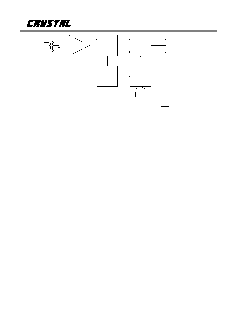
Receiver
The receiver extracts data and clock from an AMI
(Alternate Mark Inversion) coded signal and out-
puts clock and synchronized data. The receiver is
sensitive to signals over the entire range of cable
lengths and requires no equalization or ALBO
(Automatic Line Build Out) circuits. The signal is
received on both ends of a center-tapped, center-
grounded transformer. The transformer is
center-tapped on the IC side. The clock and data
recovery circuit exceeds the jitter tolerance speci-
fications of Publications 43802, 43801, 62411
amended, TR-TSY-000170, and CCITT REC.
G.823.
A block diagram of the receiver is shown in Fig-
ure 11. The two leads of the transformer (RTIP
and RRING) have opposite polarity allowing the
receiver to treat RTIP and RRING as unipolar sig-
nals. Comparators are used to detect pulses on
RTIP and RRING. The comparator thresholds are
dynamically established at a percent of the peak
level (50% of peak for E1, 65% of peak for T1;
with the slicing level selected by LEN2/1/0).
1 : 2
RTIP
RRING
RPOS
RNEG
RCLK
ACLKI or
Oscillator in Jitter
Attenuator
Data
Level
Slicer
Edge
Detector
Data
&
Clock
Sampling
Extraction
Clock
Phase
Selector
Continuously
Calibrated
Delay Line
Figure 11. Receiver Block Diagram
CS61535A
14
DS40F2

The receiver uses an edge detector and a continu-
ously calibrated delay line to generate the
recovered clock. The delay line divides its refer-
ence clock, ACLKI or the jitter attenuator's
oscillator, into 13 equal divisions or phases. Con-
tinuous calibration assures timing accuracy, even
if temperature or power supply voltage fluctuate.
The leading edge of an incoming data pulse trig-
gers the clock phase selector. The phase selector
chooses one of the 13 available phases which the
delay line produces for each bit period. The out-
put from the phase selector feeds the clock and
data recovery circuits which generate the recov-
ered clock and sample the incoming signal at
appropriate intervals to recover the data. The jitter
tolerance of the receiver exceeds that shown in
Figure 12.
The CS61535A outputs a clock immediately upon
power-up. The clock recovery circuit is cali-
brated, and the device will lock onto the AMI
data input immediately. If loss of signal occurs,
the RCLK frequency will equal the ACLKI fre-
quency.
In the Hardware Mode, data at RPOS and RNEG
is stable and may be sampled on the rising edge
of the recovered clock. In the Extended Hardware
Mode, data at RDATA is stable and may be sam-
pled on the falling edge of the recovered clock. In
the Host Mode, CLKE determines the clock po-
larity for which output data is stable and valid as
shown in Table 5.
Jitter and Recovered Clock
The CS61535A are designed for error free clock
and data recovery from an AMI encoded data
stream in the presence of more than 0.4 unit inter-
vals of jitter at high frequency. The clock
recovery circuit is also tolerant of long strings of
zeros. The edge of an incoming data bit causes
the circuitry to choose a phase from the delay line
which most closely corresponds with the arrival
time of the data edge, and that clock phase trig-
gers a pulse which is typically 140 ns in duration.
This phase of the delay line will continue to be
selected until a data bit arrives which is closer to
another of the 13 phases, causing a new phase to
be selected. The largest jump allowed along the
delay line is six phases.
When an input signal is jitter free, the phase se-
lection will occasionally jump between two
adjacent phases resulting in RCLK jitter with an
amplitude of 1/13 UIpp. These single phase
jumps are due to differences in frequency of the
incoming data and the calibration clock input to
ACLKI. For T1 operation of the CS61535A, the
instantaneous period can be 14/13 * 648 ns = 698
ns (1,662,769 Hz) or 12/13 * 648 ns = 598 ns
(1,425,231 Hz) when adjacent clock phases are
chosen. As long as the same phase is chosen, the
10
1k
10k
0
100
100k
700
.1
1
10
100
.4
28
300
300
PEAK
TO
PEAK
JITTER
(unit intervals)
JITTER FREQUENCY (Hz)
Figure 12. Input Jitter Tolerance of Receiver
MODE
(pin 5)
CLKE
(pin 28)
DATA
CLOCK
Clock Edge for
Valid Data
LOW
(<0.2V)
X
RPOS
RNEG
RCLK
RCLK
Rising
Rising
HIGH
(>(V+) - 0.2V)
LOW
RPOS
RNEG
SDO
RCLK
RCLK
SCLK
Rising
Rising
Falling
HIGH
(>(V+) - 0.2V)
HIGH
RPOS
RNEG
SDO
RCLK
RCLK
SCLK
Falling
Falling
Rising
MIDDLE
(2.5V)
X
RDATA
RCLK
Falling
X = Don't care
Table 5. Data Output/Clock Relationship
CS61535A
DS40F2
15

period will be 648 ns. Similar calculations hold
for the E1 rate.
The clock recovery circuit is designed to accept at
least 0.4 UI of jitter at the receiver. Since the data
stream contains information only when ones are
transmitted, a clock/data recovery circuit must as-
sume a zero when no signal is measured during a
bit period. Likewise, when zeros are received, no
information is present to update the clock recov-
ery circuit regarding the trend of a signal which is
jittered. The result is that two ones that are sepa-
rated by a string of zeros can exhibit maximum
deviation in pulse arrival time. For example, one
half of a period of jitter at 100 kHz occurs in 5
µ
s, which is 7.7 T1 bit periods. If the jitter ampli-
tude is 0.4 UI, then a one preceded by seven zeros
can have maximum displacement in arrival time,
i.e. either 0.4 UI too early or 0.4 UI too late. For
the CS61535A, the data recovery circuit correctly
assigns a received bit to its proper clock period if
it is displaced by less than 6/13 of a bit period
from its optimal location. Theoretically, this
would give a jitter tolerance of 0.46 UI. The ac-
tual jitter tolerance of the CS61535A is only
slightly less than the ideal.
In the event of a maximum jitter hit, the RCLK
clock period immediately adjusts to align itself
with the incoming data and prepare to accurately
place the next one, whether it arrives one period
later, or after another string of zeros and is dis-
placed by jitter. For a maximum early jitter hit,
RCLK will have a period of 7/13 * 648 ns = 349
ns (2,865,961 Hz). For a maximum late jitter hit,
RCLK will have a period of 19/13 * 648 ns = 947
ns (1,055,880 Hz).
Loss of Signal
Receiver loss of signal is indicated upon receiv-
ing 175 consecutive zeros. A digital counter
counts received zeros based on RCLK cycles. A
zero input is determined either when zeros are re-
ceived, or when the received signal amplitude
drops below a 0.3 V peak threshold.
The receiver reports loss of signal by setting the
Loss of Signal pin, LOS, high. If the serial inter-
face is used, the LOS bit will be set and an
interrupt issued on INT. LOS will go low (and
flag the INT pin again if serial I/O is used) when
a valid signal is detected. Note that in the Host
Mode, LOS is simultaneously available from both
the register and pin 12.
In a loss of signal state, the RCLK frequency will
be equal to the ACLKI frequency since ACLKI is
being used to calibrate the clock recovery circuit.
Received data is output on RPOS and RNEG (or
RDATA) regardless of LOS status. The LOS re-
turns to logic zero when the ones density reaches
12.5% (based upon 175 bit periods staring with a
one and containing less than 100 consecutive ze-
ros) as prescribed in ANSI T1.231-1993. A
power-up or manual reset will also set LOS high.
Local Loopback
The local loopback mode takes clock and data
presented on TCLK, TPOS, and TNEG (or
TDATA) and outputs it at RCLK, RPOS and
RNEG (or RDATA). Local loopback is selected
by taking pin 27 high, or LLOOP may be selected
using the serial interface. The data on the trans-
mitter inputs is transmitted on the line unless
TAOS is selected to cause the transmission of an
all ones signal instead. Receiver inputs are ig-
nored when local loopback is in effect. The jitter
attenuator is not included in the local loopback
data path. Selection of local loopback overrides
the chip's loss of signal response.
Remote Loopback
In remote loopback, the recovered clock and data
input on RTIP and RRING are sent through the
jitter attenuator and back out on the line via TTIP
and TRING. The recovered incoming signals are
also sent to RCLK, RPOS and RNEG (or
CS61535A
16
DS40F2
RDATA). Remote loopback is selected by taking
pin 26 high, or RLOOP may be selected using the
serial interface. Simultaneous selection of local
and remote loopback modes is not valid (see Re-
set).
In the CS61535A Extended Hardware Mode, re-
mote loopback occurs before the line code
encoder/decoder, insuring that the transmitted sig-
nal matches the received signal, even in the
presence of received bipolar violations. The re-
covered data will also be decoded and output on
RDATA if RCODE is low.
Driver Performance Monitor
To aid in early detection and easy isolation of
nonfunctioning links, the Hardware and Host
Modes of the CS61535A are able to monitor
transmit drive performance and report when the
driver is no longer operational. This feature can
be used to monitor either the device's perform-
ance or the performance of a neighboring driver.
The driver performance monitor indicator is nor-
mally at a low (zero) logic level, and goes to high
level upon detecting driver failure. In the Host
Mode, DPM is available from both the register
and pin 11.
The driver performance monitor consists of an ac-
tivity detector that monitors the transmitted signal
when MTIP is connected to TTIP and MRING is
connected to TRING. DPM will go high if the
absolute difference between MTIP and MRING
does not transition above or below a threshold
level within a time-out period.
Whenever more than one line interface IC resides
on the same circuit board, the effectiveness of the
driver performance monitor can be maximized by
having each IC monitor performance of a neigh-
boring device, rather than having it monitor its
own performance.
Line Code Encoder/Decoder
In Extended Hardware Mode, three line codes are
available: AMI, B8ZS and HDB3. The input to
the encoder is TDATA. The outputs from the de-
coder are RDATA and BPV (Bipolar Violation
Strobe). The encoder and decoder are selected us-
ing pins LEN2, LEN1, LEN0, TCODE a nd
RCODE as shown in Table 6.
Alarm Indication Signal
In Extended Hardware Mode, the receiver sets the
output pin AIS high when less than 9 zeros are
detected out of 8192 bit periods. AIS returns low
when 9 or more zeros are detected out of 8192
bits.
Parallel Chip Select
In Extended Hardware Mode, PCS can be used to
gate the digital control inputs: TCODE, RCODE,
LEN0, LEN1, LEN2, RLOOP, LLOOP and
TAOS. Inputs are accepted on these pins only
when PCS is low. Changes in inputs will immedi-
ately change the operating state of the device.
Therefore, when cycling PCS to update the oper-
ating state, the digital control inputs should be
stable for the entire PCS low period. The control
inputs are ignored when PCS is high.
Power On Reset / Reset
Upon power-up, the CS61535A is held in a static
state until the supply crosses a threshold of ap-
LEN 2/1/0
000
010-111
TCODE
(Transmit
Encoder
Selection)
LOW
HDB3
Encoder
B8ZS
Encoder
HIGH
AMI
Encoder
RCODE
(Receiver
Decoder
Selection)
LOW
HDB3
Decoder
B8ZS
Decoder
HIGH
AMI
Decoder
Table 6. Selection of Encoder/Decoder
CS61535A
DS40F2
17

proximately three Volts. When this threshold is
crossed, the device will delay for about 10 ms to
allow the power supply to reach operating voltage.
After this delay, calibration of the delay lines used
in the transmit and receive sections commences.
The delay lines can be calibrated only if a refer-
ence clock is present. The reference clock for the
receiver is provided by ACLKI (or by the crystal
oscillator if ACLKI is not present). The reference
clock for the transmitter is provided by TCLK. The
initial calibration should take less than 20 ms.
In operation, the delay lines are continuously cali-
brated, making the performance of the device
independent of power supply or temperature vari-
ations. The continuous calibration function
foregoes any requirement to reset the line inter-
face when in operation. However, a reset function
is available which will clear all registers.
In the Hardware and Extended Hardware modes, a
reset request is made by simultaneously setting both
RLOOP and LLOOP high for at least 200 ns. Reset
will initiate on the falling edge of the reset request
(falling edge of RLOOP and LLOOP). In the Host
Mode, a reset is initiated by simultaneously writing
RLOOP and LLOOP to the register. In either mode,
a reset will set all registers to 0 and set LOS high.
Serial Interface
In the Host Mode, pins 23 through 28 serve as a
microprocessor/microcontroller interface. One
eight-bit register can be written to via the SDI pin
or read from the SDO pin at the clock rate deter-
mined by SCLK. Through this register, a host
controller can be used to control operational char-
acteristics and monitor device status. The serial
port read/write timing is independent of the sys-
tem transmit and receive timing.
Data transfers are initiated by taking the chip se-
lect input, CS, low (CS must initially be high).
SCLK may be either high or low when CS in-
itially goes low. Address and input data bits are
clocked in on the rising edge of SCLK. Data on
SDO is valid and stable on the falling edge of
SCLK when CLKE is low, and on the rising edge
of SCLK when CLKE is high. Data transfers are
terminated by setting CS high. CS may go high
no sooner than 50 ns after the rising edge of the
SCLK cycle corresponding to the last write bit.
For a serial data read, CS may go high any time
to terminate the output.
Figure 13 shows the timing relationships for data
transfers when CLKE = 1. When CLKE = 0, data
output from the serial port, SDO, is valid on the
falling edge of SCLK. For CLKE = 1, data bit D7
is held to the falling edge of the 16th clock cycle;
for CLKE = 0, data bit D7 is held to the rising
edge of the 17th clock cycle. SDO goes to a high
CS
SCLK
SDO
SDI
D6
D5
D4
D3
D2
D1
D0
D7
0
0
D7
D6
D5
D4
D3
D2
D1
D0
Address/Command Byte
Data Input/Output
0
0
0
1
0
R/W
Figure 13. Input/Output Timing
LSB, first bit
0
R/W
Read/Write Select; 0 = write, 1 =
read
1
ADD0
LSB of address, Must be 0
2
ADD1
Must be 0
3
ADD2
Must be 0
4
ADD3
Must be 0
5
ADD4
Must be 1
6
-
Reserved - Must be 0
Table 7. Address/Command Byte
CS61535A
18
DS40F2

impedance state either after bit D7 is output or at
the end of the hold period of data bit D7.
An address/command byte, shown in Table 7,
precedes a data register. The first bit of the ad-
dress/command byte determines whether a read
or a write is requested. The next six bits contain
the address. The CS61535A responds to address
16 (0010000). The last bit is ignored.
The data register, shown in Table 8, can be writ-
ten to the serial port. Data is input on the eight
clock cycles immediately following the ad-
dress/command byte. Bits 0 and 1 are used to
clear an interrupt issued from the INT pin, which
occurs in response to a loss of signal or a problem
with the output driver. If bits 0 or 1 are true, the
corresponding interrupt is suppressed. So if a loss
of signal interrupt is cleared by writing a 1 to bit
0, the interrupt will be reenabled by writing a 0 to
bit 0. This holds for DPM as well.
Writing a "1" to either "Clear LOS" or "Clear
DPM" over the serial interface has three effects:
1) the current interrupt on the serial interface
will be cleared. (Note that simply reading the
register bits will not clear the interrupt),
2) output data bits 5, 6 and 7 will be reset as
appropriate,
3) future interrupts for the corresponding LOS
or DPM will be prevented from occuring).
Writing a "0" to either "Clear LOS" or "Clear
DPM" enables the corresponding interrupt for
LOS or DPM.
Output data from the serial interface is presented
as shown in Tables 9 and 10. Bits 2, 3 and 4 can
be read to verify line length selection. Bits 5, 6
and 7 must be decoded. Codes 101, 110 and 111
(bits 5, 6 and 7) indicate LOS and DPM state
changes. Writing a "1" to the "Clear LOS" and/or
"Clear DPM" bits in the register also resets status
bits 5, 6, and 7.
SDO goes to a high impedance state when not in
use. SDO and SDI may be tied together in appli-
c a ti on s whe re the h os t proc esso r h as a
bidirectional I/O port.
LSB: first bit in
0
clr LOS Clear Loss of Signal
1 clr DPM Clear Driver Performance Monitor
2
LEN0
Bit 0 - Line Length Select
3
LEN1
Bit 1 - Line Length Select
4
LEN2
Bit 2 - Line Lenght Select
5 RLOOP Remote Loopback
6
LLOOP Local Loopback
MSB: last bit in
7
TAOS
Transmit All Ones Select
Table 8. Input Data Register
LSB: first bit in
0
LOS
Loss of Signal
1
DPM
Driver Performance Monitor
2
LEN0
Bit 0 - Line Length Select
3
LEN1
Bit 1 - Line Length Select
4
LEN2
Bit 2 - Line Lenght Select
Table 9. Output Data Bits 0 - 4
Bits
Status
5 6 7
0 0 0
Reset has occurred or no program input.
0 0 1
TAOS in effect.
0 1 0
LLOOP in effect.
0 1 1
TAOS/LLOOP in effect.
1 0 0
RLOOP in effect
1 0 1
DPM changed state since last "clear DPM"
occured.
1 1 0
LOS changed state since last "clear LOS"
occured.
1 1 1
LOS and DPM have changed state since
last "clear LOS" and "clear DPM".
Table 10. Coding for Serial Output Bits 5, 6, 7
CS61535A
DS40F2
19

Power Supply
The device operates from a single +5 Volt supply.
Separate pins for transmit and receive supplies
provide internal isolation. These pins should be
connected externally near the device and decou-
pled to their respective grounds. TV+ must not
exceed RV+ by more than 0.3V.
Decoupling and filtering of the power supplies is
crucial for the proper operation of the analog cir-
cuits in both the transmit and receive paths. A 1.0
µ
F capacitor should be connected between TV+
and TGND, and a 0.1
µ
F capacitor should be con-
nected between RV+ and RGND. Use mylar or
ceramic capacitors and place them as closely as
possible to their respective power supply pins. A
68
µ
F tantalum capacitor should be added close
to the RV+/RGND supply. Wire wrap bread-
boarding of the line interface is not recommended
because lead resistance and inductance serve to
defeat the function of the decoupling capacitors.
Schematic & Layout Review Service
Confirm Optimum
Schematic & Layout
Before Building Your Board.
For Our Free Review Service
Call Applications Engineering.
C a l l : ( 5 1 2 ) 4 4 5 - 7 2 2 2
CS61535A
20
DS40F2
PIN DESCRIPTIONS
Hardware Mode
top
view
22
20
24
19
21
23
25
3
27
2
4
26
28
1
12
14
16
18
13
15
17
8
6
10
5
7
9
11
ACLKI
TCLK
TAOS
TPOS
LLOOP
TNEG
RLOOP
MODE
LEN2
RNEG
LEN1
RPOS
LEN0
RCLK
RGND
XTALIN
RV+
XTALOUT
RRING
DPM
RTIP
LOS
MRING
TTIP
MTIP
TGND
TRING
TV+
1
2
3
4
5
6
7
8
9
10
11
12
14
13
28
27
26
25
24
23
22
21
20
19
18
17
16
15
ACLKI
TAOS
TCLK
LLOOP
TPOS
RLOOP
TNEG
LEN2
MODE
LEN1
RNEG
LEN0
RPOS
RGND
RCLK
RV+
XTALIN
RRING
XTALOUT
RTIP
DPM
MRING
LOS
MTIP
TTIP
TRING
TGND
TV+
CS61535A
DS40F1
21

Extended Hardware Mode
1
2
3
4
5
6
7
8
9
10
11
12
14
13
28
27
26
25
24
23
22
21
20
19
18
17
16
15
ACLKI
TAOS
TCLK
LLOOP
TDATA
RLOOP
TCODE
LEN2
MODE
LEN1
BPV
LEN0
RDATA
RGND
RCLK
RV+
XTALIN
RRING
XTALOUT
RTIP
AIS
PCS
LOS
RCODE
TTIP
TRING
TGND
TV+
top
view
22
20
24
19
21
23
25
3
27
2
4
26
28
1
12
14
16
18
13
15
17
8
6
10
5
7
9
11
ACLKI
TCLK
TAOS
TDATA
LLOOP
TCODE
RLOOP
MODE
LEN2
BPV
LEN1
RDATA
LEN0
RCLK
RGND
XTALIN
RV+
XTALOUT
RRING
AIS
RTIP
LOS
PCS
TTIP
RCODE
TGND
TRING
TV+
CS61535A
22
DS40F1

Host Mode
1
2
3
4
5
6
7
8
9
10
11
12
14
13
28
27
26
25
24
23
22
21
20
19
18
17
16
15
ACLKI
CLKE
TCLK
SCLK
TPOS
CS
TNEG
SDO
MODE
SDI
RNEG
INT
RPOS
RGND
RCLK
RV+
XTALIN
RRING
XTALOUT
RTIP
DPM
MRING
LOS
MTIP
TTIP
TRING
TGND
TV+
top
view
22
20
24
19
21
23
25
3
27
2
4
26
28
1
12
14
16
18
13
15
17
8
6
10
5
7
9
11
ACLKI
TCLK
CLKE
TPOS
SCLK
TNEG
CS
MODE
SDO
RNEG
SDI
RPOS
INT
RCLK
RGND
XTALIN
RV+
XTALOUT
RRING
DPM
RTIP
LOS
MRING
TTIP
MTIP
TGND
TRING
TV+
CS61535A
DS40F1
23

Power Supplies
RGND - Ground, Pin 22.
Power supply ground for all subcircuits except the transmit driver; typically 0 Volts.
RV+ - Power Supply, Pin 21.
Power supply for all subcircuits except the transmit driver; typically +5 Volts.
TGND - Ground, Transmit Driver, Pin 14.
Power supply ground for the transmit driver; typically 0 Volts.
TV+ - Power Supply, Transmit Driver, Pin 15.
Power supply for the transmit driver; typically +5 Volts. TV+ must not exceed RV+ by more than
0.3 V.
Oscillator
XTALIN, XTALOUT - Crystal Connections, Pins 9 and 10.
A 6.176 MHz (or 8.192 MHz) crystal should be connected across these pins. If a 1.544 MHz (or
2.048 MHz) clock is provided on ACLKI (pin 1), the jitter attenuator may be disabled by tying
XTALIN, Pin 9 to RV+ through a 1 k
resistor, and floating XTALOUT, Pin 10.
Overdriving the oscillator with an external clock is not supported.
Control
ACLKI - Alternate External Clock Input, Pin 1.
The CS61535A does not require a clock signal to be input on ACLKI when a crystal is connected
between pins 9 and 10. If a clock is not provided on ACLKI, this input must be grounded. If
ACLKI is grounded, the oscillator in the jitter attenuator is used to calibrate the clock recovery
circuit and TAOS is not available.
CLKE - Clock Edge, Pin 28. (Host Mode)
Setting CLKE to logic 1 causes RPOS and RNEG to be valid on the falling edge of RCLK, and
SDO to be valid on the rising edge of SCLK. Conversely, setting CLKE to logic 0 causes RPOS
and RNEG to be valid on the rising edge of RCLK, and SDO to be valid on the falling edge of
SCLK.
CS - Chip Select, Pin 26. (Host Mode)
This pin must transition from high to low to read or write the serial port.
INT - Receive Alarm Interrupt, Pin 23. (Host Mode)
Goes low when LOS or DPM change state to flag the host processor. INT is cleared by writing
"Clear LOS" or "Clear DPM" to the register. INT is an open drain output and should be tied to
the power supply through a resistor.
CS61535A
24
DS40F1

LEN0, LEN1, LEN2 - Line Length Selection, Pins 23, 24 and 25. (Hardware and Extended
Hardware Modes)
Determines the shape and amplitude of the transmitted pulse to accommodate several cable types
and lengths. See Table 3 for information on line length selection. Also controls the receiver
slicing level and the line code in Extended Hardware Mode.
LLOOP - Local Loopback, Pin 27. (Hardware and Extended Hardware Modes)
Setting LLOOP to a logic 1 routes the transmit clock and data through to the receive clock and
data pins. TPOS/TNEG (or TDATA) are still transmitted unless overridden by a TAOS request.
Inputs on RTIP and RRING are ignored.
MODE - Mode Select, Pin 5.
Driving the MODE pin high puts the CS61535A line interface in the Host Mode. In the host
mode, a serial control port is used to control the CS61535A line interface and determine its status.
Grounding the MODE pin puts the CS61535A line interface in the Hardware Mode, where
configuration and status are controlled by discrete pins. Floating the MODE pin or driving it to
+2.5 V puts the CS61535A in Extended Hardware Mode, where configuration and status are
controlled by discrete pins. When floating MODE, there should be no external load on the pin.
MODE defines the status of 13 pins (see Table 2).
PCS - Parallel Chip Select, Pin 18. (Extended Hardware Mode)
Setting PCS high causes the CS61535A line interface to ignore the TCODE, RCODE, LEN0,
LEN1, LEN2, RLOOP, LLOOP and TAOS inputs.
RCODE - Receiver Decoder Select, Pin 17. (Extended Hardware Mode)
Setting RCODE low enables B8ZS or HDB3 zero substitution in the receiver decoder. Setting
RCODE high enables the AMI receiver decoder (see Table 8).
RLOOP - Remote Loopback, Pin 26. (Hardware and Extended Hardware Modes)
Setting RLOOP to a logic 1 causes the recovered clock and data to be sent through the jitter
attenuator (if active) and through the driver back to the line. The recovered signal is also sent to
RCLK and RPOS/RNEG (or RDATA). Any TAOS request is ignored.
Simultaneously taking RLOOP and LLOOP high for at least 200 ns initiates a device reset.
SCLK - Serial Clock, Pin 27. (Host Mode)
Clock used to read or write the serial port registers. SCLK can be either high or low when the line
interface is selected using the CS pin.
SDI - Serial Data Input, Pin 24. (Host Mode)
Data for the on-chip register. Sampled on the rising edge of SCLK.
SDO - Serial Data Output, Pin 25. (Host Mode)
Status and control information from the on-chip register. If CLKE is high SDO is valid on the
rising edge of SCLK. If CLKE is low SDO is valid on the falling edge of SCLK. This pin goes to
a high-impedance state when the serial port is being written to or after bit D7 is output.
CS61535A
DS40F1
25

TAOS - Transmit All Ones Select, Pin 28. (Hardware and Extended Hardware Modes)
Setting TAOS to a logic 1 causes continuous ones to be transmitted at the frequency determined
by ACLKI.
TCODE - Transmitter Encoder Select, Pin 4. (Extended Hardware Mode)
Setting TCODE low enables B8ZS or HDB3 zero substitution in the transmitter encoder. Setting
TCODE high enables the AMI transmitter encoder .
Data
RCLK - Recovered Clock, Pin 8.
The receiver recovered clock is output on this pin.
RDATA - Receive Data - Pin 7. (Extended Hardware Mode)
Data recovered from the RTIP and RRING inputs is output at this pin, after being decoded by the
line code decoder. RDATA is NRZ. RDATA is stable and valid on the falling edge of RCLK.
RPOS, RNEG - Receive Positive Data, Receive Negative Data, Pins 6 and 7. (Hardware and
Host Modes)
The receiver recovered NRZ digital data is output on these pins. In the Hardware Mode, RPOS
and RNEG are stable and valid on the rising edge of RCLK. In the Host Mode, CLKE determines
the clock edge for which RPOS and RNEG are stable and valid. See Table 5. A positive pulse
(with respect to ground) received on the RTIP pin generates a logic 1 on RPOS, and a positive
pulse received on the RRING pin generates a logic 1 on RNEG.
RTIP, RRING - Receive Tip, Receive Ring, Pins 19 and 20.
The AMI receive signal is input to these pins. A center-tapped, center-grounded, 2:1, step-up
transformer is required on these inputs, as shown in Figure A1 in the Applications section. Data
and clock are recovered and output on RCLK and RPOS/RNEG or RDATA.
TCLK - Transmit Clock, Pin 2.
The1.544 MHz (or 2.048 MHz) transmit clock is input on this pin. TPOS/TNEG or TDATA are
sampled on the falling edge of TCLK.
TDATA - Transmit Data, Pin 3. (Extended Hardware Mode)
Transmitter NRZ input data which passes through the line code encoder, and is then driven on to
the line through TTIP and TRING. TDATA is sampled on the falling edge of TCLK.
TPOS, TNEG - Transmit Positive Data, Transmit Negative Data, Pins 3 and 4. (Hardware and
Host Modes)
Inputs for clock and data to be transmitted. The signal is driven on to the line through TTIP and
TRING. TPOS and TNEG are sampled on the falling edge of TCLK. A TPOS input causes a
positive pulse to be transmitted, while a TNEG input causes a negative pulse to be transmitted.
TTIP, TRING - Transmit Tip, Transmit Ring, Pins 13 and 16.
The AMI signal is driven to the line through these pins. In the CS61535A, this output is designed
to drive a 75
load. A 1:1, 1:1.15 or 1:1.26 transformer is required as shown in Figure A1.
CS61535A
26
DS40F1

Status
AIS - Alarm Indication Signal, Pin 11. (Extended Hardware Mode)
AIS goes high when unframed all-ones condition (blue alarm) is detected, using the detection
criteria of less than three zeros out of 2048 bit periods.
BPV- Bipolar Violation Strobe, Pin 6. (Extended Hardware Mode)
BPV strobes high when a bipolar violation is detected in the received signal. B8ZS (or HDB3)
zero substitutions are not flagged as bipolar violations if the B8ZS (or HDB3) decoder has been
enabled.
DPM - Driver Performance Monitor, Pin 11. (Hardware and Host Modes)
DPM goes high if no activity is detected on MTIP and MRING.
LOS - Loss of Signal, Pin 12.
LOS goes high when 175 consecutive zeros have been received. For the CS61535A, LOS returns
low when the ones density reaches 12.5% (based upon 175 bit periods starting with a one and
containing less than 100 consecutive zeros) as prescribed by ANSI T1.231-1993.
MTIP, MRING - Monitor Tip, Monitor Ring, Pins 17 and 18. (Hardware and Host Modes)
These pins are normally connected to TTIP and TRING and monitor the output of a CS61535A.
If the INT pin in the host mode is used, and the monitor is not used, writing "Clear DPM" to the
serial interface will prevent an interrupt from the driver performance monitor.
CS61535A
DS40F1
27

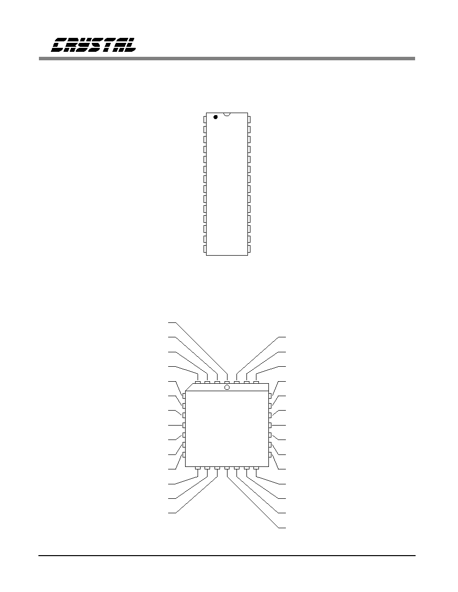
28 pin
Plastic DIP
1
28
15
14
MILLIMETERS
INCHES
DIM
MIN
MAX
MIN
MAX
D
B
A
L
C
13.72
14.22 0.540
0.560
36.45
1.02
0.36
0.51
3.94
3.18
0.20
0∞
15.24
37.21
1.65
0.56
1.02
5.08
3.81
0.38
15∞
1.435
0.040
0.014
0.020
0.155
0.125
0.600
0.008
0∞
1.465
0.065
0.022
0.040
0.200
0.150
0.015
15∞
15.87
0.625
2.41
2.67 0.095
0.105
C
eA
E1
D
B
SEATING
PLANE
A
B1
e1
A1
L
NOTES:
1. POSITIONAL TOLERANCE OF LEADS SHALL BE WITHIN
0.25mm (0.010") AT MAXIMUM MATERIAL CONDITION, IN
RELATION TO SEATING PLANE AND EACH OTHER.
2. DIMENSION eA TO CENTER OF LEADS WHEN FORMED PARALLEL.
3. DIMENSION E1 DOES NOT INCLUDE MOLD FLASH.
NOM
13.97
36.83
1.27
0.46
0.76
4.32
-
0.25
-
-
2.54
NOM
0.550
1.450
0.050
0.018
0.030
0.170
-
-
0.010
-
0.100
A1
B1
E1
e1
eA
E
E1
D1
D
D2/E2
28-pin PLCC
28
D2/E2
MAX
MIN
MAX
MIN
MILLIMETERS
INCHES
DIM
A
4.57
4.20
0.180
0.165
D/E
12.32
12.57 0.485
0.495
B
0.53
0.33
0.021
0.013
e
A
A1
B
e
2.29
0.090
11.43
11.58 0.450
0.456
9.91
10.92 0.390
0.430
1.19
1.35 0.047
0.053
NOM
4.45
12.45
0.41
2.79
11.51
10.41
1.27
NOM
0.175
0.490
0.016
0.110
0.453
0.410
0.050
3.04
0.120
D1/E1
A1
CS61535A
28
DS40F1

APPLICATIONS
Line Interface
Figures A1-A3 show the typical configurations
for interfacing the I.C. to a line through transmit
and receive transformers.
The receiver transformer is center tapped and
center grounded with resistors between the center
tap and each leg on the I.C. side. These resistors
provide the termination for the line.
Figures A1-A3 show a 0.47
µ
F capacitor in series
with the transmit transformer primary. This ca-
pacitor is needed to prevent any buildup in the
core of the transformer due to any DC imbalance
that may be present at the differential outputs,
TTIP and TRING. If DC saturates the trans-
former, a DC offset will result during the
transmission of a space (zero) as the transformer
tries to dump the charge and return to equilib-
rium. The blocking capacitor will keep DC
current from flowing in the transformer.
Selecting an Oscillator Crystal
Specific crystal parameters are required for
proper operation of the CS61535A. It is recom-
me n de d th a t t h e C XT617 6 from Cry st al
Control
&
Monitor
Frame
Format
Encoder/
Decoder
CS61535A
IN
HOST
MODE
RECEIVE
LINE
TRANSMIT
LINE
28
1
12
11
5
7
6
8
3
4
2
9
10
XTL
RV+
+
68
µ
F
RGND
0.1
µ
F
+5V
21
15
+
1.0
µ
F
TGND
RV+
TV+
CLKE
ACLKI
LOS
DPM
MODE
RPOS
RNEG
RCLK
TPOS
TNEG
TCLK
XTALIN
XTALOUT
RGND
TGND
22
14
SCLK
CS
INT
SDI
SDO
RTIP
RRING
MTIP
MRING
TRING
TTIP
19
20
17
18
16
13
R1
R2
0.47
µ
F
CT 2:1
µ
P
Serial
Port
27
26
23
24
25
+5V
100 k
DEVICE
FREQUENCY
MHz
CABLE
R1&2
Transmit
Transformer
CS61535A
1.544
2.048
2.048
100
120
75
200
240
150
1:1.15
1:1.26
1:1
Figure A1. Host Mode Configuration
CS61535A
DS40F2
29

Control
&
Monitor
Frame
Format
Encoder/
Decoder
CS61535A
IN
HARDWARE
MODE
Line
Length
Setting
RECEIVE
LINE
TRANSMIT
LINE
28
1
26
27
5
7
6
8
3
4
2
9
10
XTL
+
68
µ
F
RGND
0.1
µ
F
+5V
21
15
+
1.0
µ
F
TGND
RV+
TV+
TAOS
ACLKI
RLOOP
LLOOP
MODE
RPOS
RNEG
RCLK
TPOS
TNEG
TCLK
XTALIN
XTALOUT
RGND
TGND
22
14
LEN0
LEN1
LEN2
RTIP
RRING
MTIP
MRING
TRING
TTIP
23
24
25
19
20
17
18
16
13
R1
R2
0.47
µ
F
CT 2:1
12
11
LOS
DPM
Figure A2. Hardware Mode Configuration
Control
&
Monitor
Frame
Format
Encoder/
Decoder
CS61535A
IN
EXTENDED
HARDWARE
MODE
Line
Length
Setting
RECEIVE
LINE
TRANSMIT
LINE
17
18
6
28
5
7
8
3
2
9
10
XTL
+
68
µ
F
RGND
0.1
µ
F
+5V
21
15
+
1.0
µ
F
TGND
RV+
TV+
RCODE
PCS
BPV
TAOS
MODE
RDATA
RCLK
TDATA
TCLK
XTALIN
XTALOUT
RGND
TGND
22
14
LEN0
LEN1
LEN2
RTIP
RRING
TRING
TTIP
23
24
25
19
20
16
13
R1
R2
0.47
µ
F
CT 2:1
1
26
ACLKI
RLOOP
27
12
LLOOP
LOS
11
AIS
4
TCODE
Figure A3. Extended Hardware Mode Configuration
CS61535A
30
DS40F2
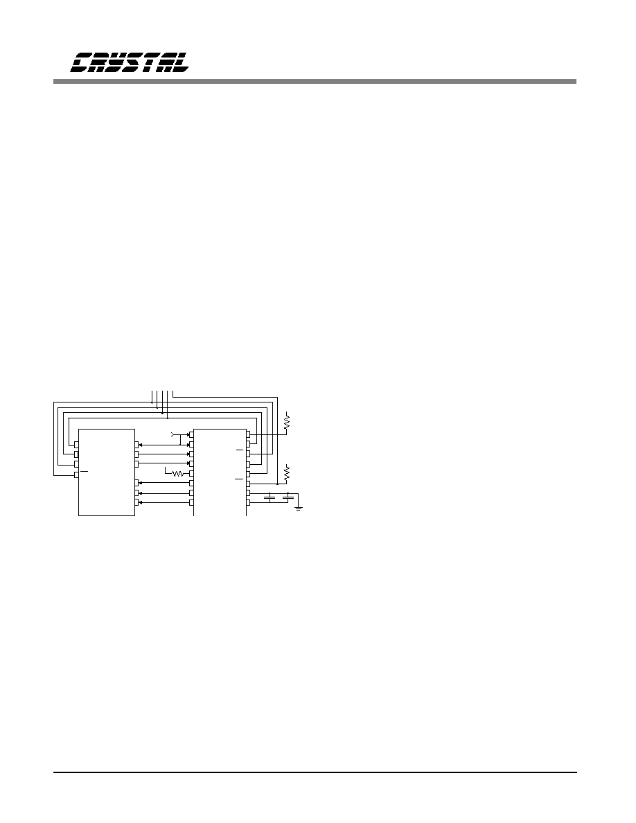
Semiconductor be used for T1 applications, and
that the CXT8192 be used for E1 applications.
Interfacing The CS61535A With the CS62180B
T1 Transceiver
To interface with the CS62180B, connect the de-
vices as shown in Figure A4. In this case, the
CS61535A and CS62180B are in Host Mode con-
trolled by a microprocessor serial interface. If the
CS61535A is used in Hardware Mode, then the
CS61535A RCLK output must be inverted before
being input to the CS62180B. If the CS61535A is
used in Extended Hardware Mode, the CS61535A
RCLK output does not need to be inverted before
being input to the CS62180B.
CS61534 Compatibility
The CS61535A is pin compatible with the
CS61534. The CS61535A has greater jitter toler-
ance for both transmitter and receiver, and it
provides more jitter attenuation starting at jitter
frequencies of 6 Hz. The greater jitter tolerance
and attenuation in the transmit path makes the
CS61535A more suitable for CCITT demultiplex-
ing applications where eight bits can be dropped
from the clock/data stream at once. Similarly,
these parts can be used in SONET applications
with the addition of some external circuitry.
The main differences of the CS61535A relative
to the CS61534 is:
1) On the CS61535A, selection of LEN 2/1/0 =
0/0/0 changes the voltage at which the receiver
accepts an input as a pulse (slicing level) from
65% to 50% of the peak pulse amplitude. Lower-
ing the data slicing level will improve receiver
sensitivity at long cable lengths when the data is
jittered. A 50% slicing level will also improve
crosstalk sensitivity for channels where received
pulses do not have undershoot.
2) There are differences in the functionality of the
ACLKI (ACLK) input on the CS61534 and
CS61535A. ACKLI (ACLK) is used as the trans-
mit clock in the transmit all ones (TAOS) mode.
On the CS61535A, ACLKI is used as a calibra-
tion reference for the receiver clock recovery
circuit and therefore may not be supplied by
RCLK. On the CS61534, ACLK may be supplied
by RCLK . If an external clock is not provide on
the ACLKI input of the CS61535A, the crystal
oscillator is used to calibrate the receiver clock
recovery circuit.
3) On the CS61535A, the Host Mode status regis-
ter bits 5, 6 and 7 are encoded so that state
changes on LOS and DPM may be reported.
4) RCLK on the CS61534 has a 50% duty cycle,
while RCLK on the CS61535A has a duty cycle
which is typically 30% or 70%. Also, the
CS61535A RCLK duty cycle and instantaneous
frequency vary with received jitter and may ex-
hibit 1/13 UIpp quantization jitter even when the
incoming signal is jitter free.
5) The CS61535A requires 25 ns of setup time on
TPOS and TNEG before the falling edge of
TCLK and 25 ns of hold time on these inputs af-
ACLKI
TCLK
RGND
RCLK
RV+
+5V
0V
0.1uF
RPOS
RNEG
TPOS
TNEG
CS62180B
MODE
V+
CLKE
SCLK
SDO
SDI
TCLK
TPOS
TNEG
RNEG
RPOS
RCLK
SCLK
SDO
SDI
TO HOST CONTROLLER
V+
100k
100k
1.544 MHz
CLOCK
CS61535A
CS
V+
22k
SIGNAL
68uF
+
CS
INT
Figure A4. Interfacing the CS61535A with the
CS62180B (Host Mode)
CS61535A
DS40F2
31

ter the falling edge of TCLK. The CS61534 re-
quires 50 ns of hold time on TPOS and TNEG
after the falling edge of TCL, and 0 ns of setup
time.
6) LOS occurs after 31 consecutive zeros on the
CS61534. For the CS61535A LOS occurs after
175 zeros.
7) Since the CS61535A receivers are continu-
ously calibrated, there is no need to issue a reset
to initialize the receiver timing as with the
CS61534.
Using the CS61535A for SONET
The CS61535A can be applied to SONET VT1.5
and VT2.0 interface circuits as shown in Fig-
ure A5. The SONET data rate is 51.84 MHz, and
has 6480 bits per frame (125 us per frame). An
individual T1 frame (193 bits per frame) or PCM-
30 frame (256 bits per frame) has its data mapped
into the 6480 bit SONET frame. The mapping
does not result in a uniform spacing between
sucessive T1 (or E1) bits. Rather, for locked VT
applications, gaps as large as 24 T1 bit periods or
32 E1 bit periods can exist between successive
bits. With floating VTs, the gaps can be even
larger.
The circuit in Figure A5 eliminates the demulti-
plexing jitter in a two-step approach. The first
step uses a FIFO which is filled at a 51.84 MHz
rate (when T1 or E1 bits are present), and which
is emptied at a sub-multiple of the 51.84 rate. The
FIFO is emptied only when it contains data.
When the FIFO is empty the output clock is not
pulsed.
The sub-multiple rate chosen should be slightly
faster than the target rate (1.544 or 2.048 MHz),
but as close to the target rate as possible. For
TPOS
TCLK2
TNEG
RPOS
RNEG
RCLK2
TCLK1
TSER
RSER
RCLK1
FIFO
FIFO
51.84 MHz
Div By
Empty
Write
Clock
TSER
RSER
RCLK2
CS62180B
Driver
Receiver
CS61535A
6480 to
193 bit
(or 256 bit)
Mapping
Circuit
Jitter
Attenuator
Figure A5. SONET Application
CS61535A
32
DS40F2

locked VT operation, Table A1 shows potential
sub-multiple data rates, and the impact on those
rates on the maximum gap in the output clock of
the FIFO, and depth of FIFO required. FIFO
depth will have to be increased for floating VT
operation, with 8 bits of FIFO depth being added
for each pointer alignment change that can occur.
The objective that should be met in picking a
FIFO depth and clock divider is keep the maxi-
mum gap on the output of the FIFO at 12 bits or
less. Twelve bits is the maximum jitter which can
be input to the CS61535A's jitter attenuator with-
out causing the overflow/undeflow protection
circuit to operate. The CS61535A then removes
the remaining jitter from the signal.
The receive path also requires a bit mapping
(from 193 or 256 bits to 6480 bits). This mapping
requires an input buffer with the same depth as
use on the transmit path. This buffer also absorbs
the output jitter generated by the CS61535A's
digital clock recovery.
Transformers
Recommended transmitter and receiver trans-
former specifications for the CS61535A are
shown in Table A2. The transformers in Table A3
have been tested and recommended for use with
the CS61535A. Refer to the "Telecom Trans-
former Selection Guide" for detailed schematics
which show how to connect the line interface IC
with a particular transformer.
In applications with the CS61535A where it is ad-
vantageous to use a single transmitter transformer
for both 75
and 120
E1 applications, a 1:1.26
transforer may be used. Although transmitter re-
turn loss will be reduced for 75
applications, the
pulse amplitude will be correct across a 75
load.
Target Rate
(MHz)
Clock
Divider
Resultant
Rate (MHz)
Maximum Gap
FIFO Depth
Required
(
µ
s)
bits
1.544
32
1.620
6.2
10
21
1.544
33
1.571
3.9
6
26
2.048
25
2.074
3.4
7
34
Table A1. Locked VT FIFO Analysis
Parameter
CS61535A Receiver
CS61535A Transmitter
Turns Ratio
1:2 CT
±
5%
1:1
±
1.5 % for 75
E1
1:1.15
±
5 % for 100
T1
1:1.26
±
1.5 % for 120
E1
Primary Inductance
600
µ
H min. @ 772 kHz
1.5 mH min. @ 772 kHz
Primary Leakage Inductance
1.3
µ
H max. @ 772 kHz
0.3
µ
H max. @ 772 kHz
Secondary Leakage Inductance
0.4
µ
H max. @ 772 kHz
0.4
µ
H max. @ 772 kHz
Interwinding Capacitance
23 pF max.
18 pF max.
ET-constant
16 V-
µ
s min. for T1
12 V-
µ
s min. for E1
16 V-
µ
s min. for T1
12 V-
µ
s min. for E1
Table A2. Transformer Specifications
CS61535A
DS40F2
33

Application
Turns
Ratio(s)
Manufacturer
Part Number
Package Type
RX:
T1 & E1
1:2CT
Pulse Engineering
PE-65351
1.5 kV through-hole, single
Schott
67129300
Bel Fuse
0553-0013-HC
TX:
T1
1:1.15
Pulse Engineering
PE-65388
1.5 kV through-hole, single
Schott
67129310
Bel Fuse
0553-0013-RC
TX:
E1 (75 & 120
)
1:1.26
1:1
Pulse Engineering
PE-65389
1.5 kV through-hole, single
Schott
67129320
Bel Fuse
0553-0013-SC
RX &TX:
T1
1:2CT
1:1.15
Pulse Engineering
PE-65565
1.5 kV through-hole, dual
Bel Fuse
0553-0013-7J
RX &TX:
E1 (75 & 120
)
1:2CT
1:1.26
1:1
Pulse Engineering
PE-65566
1.5 kV through-hole, dual
Bel Fuse
0553-0013-8J
RX &TX:
T1
1:2CT
1:1.15
Pulse Engineering
PE-65765
1.5 kVsurface-mount, dual
Bel Fuse
S553-0013-06
RX &TX:
E1 (75 & 120
)
1:2CT
1:1.26
1:1
Pulse Engineering
PE-65766
1.5 kV surface-mount, dual
Bel Fuse
S553-0013-07
RX :
T1 & E1
1:2CT
Pulse Engineering
PE-65835
3 kV through-hole, single
EN60950, EN41003 approved
TX:
E1 (75 & 120
)
1:1.26
1:1
Pulse Engineering
PE-65839
3 kV through-hole, single
EN60950, EN41003 approved
Table A3. Recommended Transformers For The CS61535A
CS61535A
34
DS40F2

Features
∑
Socketed Line Interface Device
∑
All Required Components for Complete
Line Interface Evaluation
∑
Configuration by DIP Switch or Serial
Interface
∑
LED Status Indicators for Alarm
Conditions
∑
Support for Host, Hardware, and
Extended Hardware Modes
General Description
The evaluation board includes a socketed line interface
device and all support components necessary for
evaluation. The board is powered by an external 5 Volt
supply.
The board may be configured for 100
twisted-pair
T1, 75
coax E1, or 120
twisted-pair E1 operation.
Binding posts are provided for line connections. Sev-
eral BNC connectors are available to provide system
clocks and data I/O. Two LED indicators monitor de-
vice alarm conditions. The board supports all line
interface operating modes.
ORDERING INFORMATION:
CDB61534, CDB61535.
CDB61535A,
CDB6158, CDB6158A,
CDB61574,
CDB61574A, CDB61575, CDB61577,
CDB61304A, CDB61305A
SEP '95
DS40DB3
35
Crystal Semiconductor Corporation
P.O. Box 17847, Austin, TX 78760
(512) 445-7222 FAX: (512) 445-7581
Line Interface Evaluation Board
CDB61534, CDB61535, CDB61535A, CDB6158,
CDB6158A, CDB61574, CDB61574A, CDB61575,
CDB61577, CDB615304A, & CDB61305A
ACLKI
TCLK
TPOS
(TDATA)
TNEG
RNEG
(BPV)
RPOS
(RDATA)
RCLK
CS61534,
CS61535,
CS61535A,
CS6158,
CS6158A,
CS61574,
CS61574A,
CS61575,
CS61577,
CS61304A
or
CS61305A
Reset
Circuit
Mode Select
Circuit
(TCODE)
+5V
0V
LED Status
Indicators
Hardware
Control Circuit
Serial Interface
Control Circuit
TTIP
TRING
RTIP
RRING
XTL

POWER SUPPLY
As shown on the evaluation board schematic in
Figure 1, power is supplied to the evaluation
board from an external +5 Volt supply connected
to the two binding posts labeled +5V and GND.
Transient suppressor D10 protects the compo-
nents on the board from over-voltage damage and
reversed supply connections. The recommended
power supply decoupling is provided by C1, C2
and C3. Ceramic capacitor C1 and electrolytic ca-
pacitor C2 are used to decouple RV+ to RGND.
Capacitor C3 decouples TV+ to TGND. The TV+
and RV+ power supply traces are connected at the
device socket U1. A ground plane on the compo-
nent side of the evaluation board insures optimum
performance.
BOARD CONFIGURATION
Pins on line interface device U1 with more than
one pin name have different functions depending
on the operating mode selected. Pin names not
enclosed in parenthesis or square brackets de-
scribe the Hardware mode pin function. Pin
names enclosed in parenthesis describe the Ex-
tended Hardware mode pin function. Pin names
enclosed in square brackets describe the Host
mode pin function.
Table 1 explains how to configure the evaluation
board jumpers depending on the device installed
and the desired operating mode. Mode selection
is accomplished with slide switch SW1 and jump-
e rs JP2 , JP6, and JP7 . The CS61 535 A,
CS61574A, CS61575, CS61577, CS61304A, and
CS61305A support the Hardware, Extended
Hardware, and Host operating modes. The
CS61534, CS61535, and CS61574 support the
Hardware and Host operating modes. The
CS6158 and CS6158A only support the Hardware
operating mode.
Hardware Mode
In the Hardware operating mode, the line inter-
face is configured using DIP switch S2. The digi-
tal control inputs to the device selected by S2 in-
clude: transmit all ones (TAOS), local loopback
(LLOOP), remote loopback (RLOOP), and trans-
mit line length selection (LEN2,LEN1,LEN0).
Closing a DIP switch on S2 towards the label sets
the device control pin of the same name to logic 1
(+5 Volts). Note that S2 switch positions TCODE
and RCODE have no function in Hardware mode.
In addition, the host processor interface connector
JP1 should not be used in the Hardware mode.
Two LED status indicators are provided in Hard-
ware mode. The LED labeled DPM (AIS) illumi-
nates when the line interface asserts the Driver
JUMPER
POSITION
FUNCTION SELECTED
JP1
-
Connector for external processor in Host operating mode.
JP2, JP6, JP7
A-A
Extended Hardware operating mode.
B-B
Hardware or Host operating modes.
JP3
IN
Hardware or Extended Hardware operating modes.
OUT
Host operating mode.
JP4
C-C
Connects the ACLKI BNC input to pin 1 of device.
D-D
Grounds the ACLKI BNC input through 51
resistor R1.
JP5
E-E
Transmit line connection for all applications except those listed for "F-F" on the next line.
F-F
75
coax E1 applications using the Schott 12932/12532 or PE-65389/65566 at transformer T1.
JP8
IN
Shorts resistor R2 for all applications except those listed for "OUT" on the next line.
OUT
Inserts resistor R2 for 75
coax E1 applications using the CS61534, 35, 58, 74, or 77.
Table 1. Evaluation Board Jumper Settings
LINE INTERFACE EVALUATION BOARD
36
DS40DB3

R16
1k
8
RCLK
2
TCLK
3
TPOS
(TDATA)
6
RNEG
(BPV)
Pin 3
TCLK
RCLK
Pin 6
4
TNEG
7
RPOS
(RDATA)
1
ACLKI
Pin 7
ACLKI
R1 51.1
Pin 4
S2
R15
100
RV+
RV+
Q1
2N2222
R6
470
LED
D3
RV+
Q2
2N2222
R5
470
LED
D2
JP1
D9
1N914
D8
R14
4.7k
SIP
RV+
LOS
DPM
(AIS)
MODE
R18
10k
R17
10k
5
11
12
23
24
25
26
27
28
LEN1/SDI
LEN2/SD0
LLOOP/SCLK
TAOS/CLKE
TCODE
RLOOP/CS
SDI
SDO
SCLK
INT
CS
LEN0/INT
S1
RESET
MODE
SW1
R4
221k
A
A
B
B
D
D
C
C
JP4
JP2
RCODE
C4 0.047
µ
F
3
6
8
7
5
1
2
4
HOST:3-1,6-8
EXT HW: 3-2, 6-7
HW: 3-4, 6-5
18
TRING
TTIP
0.47
µ
F
C5
TRING
TTIP
+5V
22
14
15
RV+
TV+
TGND
RGND
D10
P6KE
21
T1
(see Table 2)
17
C2
0.1
µ
F
C1
68
µ
F
19
RTIP
RRING
RRING
RTIP
20
JP8
R2
4.4
C3
1
µ
F
RV+
RCLK
TCLK
RNEG (BPV)
ACLKI
LEN1 [SDI]
LEN2 [SD0]
LLOOP [SCLK]
TAOS [CKLE]
XTALIN
{CS6158/58A: RT}
XTALOUT
{CS6158/58A: NC}
LOS
DPM (AIS)
MODE
13
16
A
A
A
A
B
B
B
B
RTIP
RRING
TRING
Pin 17
Pin 18
9
10
TTIP
RV+
R13 (only included for CS6158/58A)
1k
(Used only for E1 75
applications with the CS61534,
CS61535, CS6158, CS61574,
OR CS61577)
CS61534, CS61535,
CS61535A, CS6158,
CS6158A, CS61574,
CS61574A, CS61575,
CS61577, CS61304A,
OR CS61305A
U1:
F
F
E
E
Prototyping
Area
RV+
LEN0 [INT]
RLOOP [CS]
MRING (PCS)
RPOS (RDATA)
TPOS (TDATA)
MTIP (RCODE)
JP6
JP7
JP5
E1: CXT8192
T1: CXT6176
(not included for CS6158/58A)
+
TNEG (TCODE)
U1
R9
200
R10
200
T2
(see Table 2)
2:1
GND
(0V)
Change R9 and R10 for E1 operation
Figure 1. Evaluation Board Schematic
LINE INTERFACE EVALUATION BOARD
DS40DB3
37

Performance Monitor alarm. The LED labeled
LOS illuminates when the line interface receiver
has detected a loss of signal.
Extended Hardware Mode
In the Extended Hardware operating mode, the
line interface is configured using DIP switch S2.
The digital control inputs to the device selected
by S2 include: transmit all ones (TAOS), local
loopback (LLOOP), remote loopback (RLOOP),
transmit line length selection (LEN2, LEN1,
LEN0), transmit line code (TCODE), and receive
line code (RCODE). Closing a DIP switch (mov-
ing it towards the S2 label) sets the device control
pin of the same name to logic 1 (+5 Volts). Note
that the TCODE and RCODE options are active
low and are enabled when the switch is moved
away from the S2 label. The parallel chip select
input PCS is tied to ground in Extended Hard-
ware mode to enable the device to be reconfig-
ured when S2 is changed. In addition, the host
processor interface connector JP1 should not be
used in Extended Hardware mode.
Two LED status indicators are provided in Ex-
tended Hardware mode. The LED labeled DPM
(AIS) illuminates when the line interface detects
the receive blue alarm (AIS). The LED labeled
LOS illuminates when the line interface receiver
has detected a loss of signal.
Host Mode
In the Host operating mode, the line interface is
configured using a host processor connected to
the serial interface port JP1. The S2 switch posi-
tion labeled CLKE selects the active edge of
SCLK and RCLK. Closing the CLKE switch se-
lects RPOS and RNEG to be valid on the falling
edge of RCLK and SDO to be valid on the rising
edge of SCLK as required by the CS2180B T1
framer.
All other DIP switch positions on S2 should be
open (logic 0) to prevent shorting of the serial in-
terface signals. Resistor R15 is a current limiting
resistor that prevents the serial interface signals
from being shorted directly to the +5 Volt supply
if any S2 switch, other than CLKE, is closed.
Jumper JP3 should be out so the INT pin may be
externally pulled-up at the host processor inter-
rupt pin.
Two LED status indicators are provided in Host
mode. The LED labeled DPM (AIS) illuminates
when the line interface asserts the Driver Per-
formance Monitor alarm. The LED labeled LOS
illuminates when the line interface receiver has
detected a loss of signal.
Manual Reset
A manual reset circuit is provided that can be
used in Hardware and Extended Hardware
modes. The reset circuit consists of S1, R4, R16,
C4, D8, and D9. Pressing switch S1 forces both
LLOOP and RLOOP to a logic 1 and causes a
reset. A reset is only necessary for the CS61534
device to calibrate the center frequency of the re-
ceiver clock recovery circuit. All other line inter-
face units use a continuously calibrated clock re-
covery circuit that eliminates the reset require-
ment.
TRANSMIT CIRCUIT
The transmit clock and data signals are supplied
on BNC inputs labeled TCLK, TPOS(TDATA),
and TNEG. In the Hardware and Host operating
modes, data is supplied on the TPOS(TDATA)
and TNEG connectors in dual NRZ format. In the
Extended Hardware operating mode, data is sup-
plied in NRZ format on the TPOS(TDATA) con-
nector and TNEG is not used.
The transmitter output is transformer coupled to
the line through a transformer denoted as T1 in
Figure 1. The signal is available at the TTIP and
TRING binding posts. Capacitor C5 is the recom-
mended 0.47
µ
F DC blocking capacitor.
LINE INTERFACE EVALUATION BOARD
38
DS40DB3

The evaluation board supports 100
twisted-pair
T1, 75
coax E1, and 120
twisted-pair E1 op-
eration. The CDB61534, CDB61535, CDB6158,
CDB61574, and CDB61577 are supplied from
the factory with a 1:2 transmit transformer that
may be used for all T1 and E1 applications. The
C DB 61 5 35 A, C DB 6 15 8A, CDB 615 74A,
CDB61575, CDB61304A, and CDB61305A are
supplied with a 1:1.15 transmit transformer in-
stalled for T1 applications. An additional 1:1:1.26
transformer for E1 applications is provided with
the board. This transformer requires JP5 to be
jumpered across F-F for 75
coax E1 applica-
tions.
T h e C DB 61 5 34 , C DB 6 15 3 5, C DB61 58,
CDB61574, and CDB61577 require the JP8
jumper to be out for 75
coax E1 applications.
This inserts resistor R2 to reduce the transmit
pulse amplitude and meet the 2.37 V nominal
pulse amplitude requirement in CCITT G.703. In
addition, R2 increases the equivalent load imped-
ance across TTIP and TRING.
RECEIVE CIRCUIT
The receive line interface signal is input at the
RTIP and RRING binding posts. The receive sig-
nal is transformer coupled to the line interface de-
vice through a center-tapped 1:2 transformer. The
transformer produces ground referenced pulses of
equal amplitude and opposite polarity on RTIP
and RRING.
The receive line interface is terminated by resis-
tors R9 and R10. The evaluation boards are sup-
plied from the factory with 200
resistors for ter-
minating 100
T1 twisted-pair lines. Resistors
R9 and R10 should be replaced with 240
resis-
tors for terminating 120
E1 twisted-pair lines or
150
resistors for terminating 75
E1 coaxial
lines. Two 243
resistors and two 150
resistors
are included with the evaluation board for this
purpose.
The recovered clock and data signals are avail-
a b le on B NC o u tp u ts la b el e d RC L K,
RPOS(RDATA), and RNEG(BPV). In the Hard-
ware and Host operating modes, data is output on
the RPOS(RDATA) and RNEG(BPV) connectors
in dual NRZ format. In the Extended Hardware
operating mode, data is output in NRZ format on
the RPOS(RDATA) connector and bipolar viola-
tions are reported on the RNEG(BPV) connector.
QUARTZ CRYSTAL
A quartz crystal must be installed in socket Y1 for
all devices except the CS6158 and CS6158A. A
Crystal Semiconductor CXT6176 crystal is rec-
ommended for T1 operation and a CXT8192 is
recommended for E1 operation. The evaluation
board has a CXT6176 installed at the factory and
a CXT8192 is also provided with the board.
The CDB6158 and CDB6158A have resistor R13
installed instead of a crystal. This connects the RT
pin of the device to the +5 Volt supply.
ALTERNATE CLOCK INPUT
The ACLKI BNC input provides the alternate
clock reference for the line interface device
(ACLK for the CS61534) when JP4 is jumpered
across C-C. This clock is required for the
CS61534, CS61535, CS6158, and CS6158A op-
eration but is optional for all other line interface
devices. If ACLKI is provided, it may be desir-
able to connect both C-C and D-D positions on
JP4 to terminate the external clock source provid-
ing ACLKI with the 51
resistor R1. If ACLKI is
optional and not used, connector JP4 should be
jumpered across D-D to ground pin 1 of the de-
vice through resistor R1.
TRANSFORMER SELECTION
To permit the evaluation of other transformers,
Table 2 lists the transformer and line interface de-
vice combinations that can be used in T1 and E1
LINE INTERFACE EVALUATION BOARD
DS40DB3
39

applications. A letter at the intersection of a row
and column in Table 2 indicates that the selected
transformer is supported for use with the device.
The transformer is installed in the evaluation
board with pin 1 positioned to match the letter
illustrated on the drawing in Table 2. For exam-
ple, the Pulse Engineering PE-65388 transformer
may be used with the transmitter of the CS61575
device for 100
T1 applications only (as indi-
cated by note 3) when installed in transformer
socket T1 with pin 1 at position D (upper right).
PROTOTYPING AREA
A prototyping area with power supply and ground
connections is provided on the evaluation board.
This area can be used to develop and test a vari-
ety of additional circuits like a data pattern gener-
ator, CS2180B framer, system synchronizer PLL,
or specialized interface logic.
EVALUATION HINTS
1. Properly terminate TTIP/TRING when evaluat-
ing the transmit output signal. For more informa-
tion concerning pulse shape evaluation, refer to
the Crystal application note entitled "Measure-
ment and Evaluation of Pulse Shapes in T1/E1
Transmission Systems."
2. Change the receiver terminating resistors R9
and R10 when evaluating E1 applications. Resis-
tors R9 and R10 should be replaced with 240
resistors for terminating 120
E1 twisted-pair
lines or 150
resistors for terminating 75
E1
coaxial lines. Two 243
resistors and two 150
resistors are included with the evaluation board
for this purpose.
3. Closing a DIP switch on S2 towards the label
sets the device control pin of the same name to
logic 1 (+5 Volts).
4. To avoid damage to the external host controller
connected to JP1, all S2 switch positions (except
CLKE) should be open. In the Host operating
mode, the CLKE switch selects the active edge of
SCLK and RCLK.
LINE INTERFACE EVALUATION BOARD
40
DS40DB3
NOTES:
1. A letter at the intersection of a row and column in Table 2 indicates
that the selected transformer is supported for use with the device.
The transformer is installed in the evaluation board with pin 1 po-
sitioned to match the letter illustrated in the drawing to the left.
2. The receive transformer (RX) is soldered at location T2 on the
evaluation board and is used for all applications. The transmit
transformer (TX) is socketed at location T1 on the evaluation
board and may be changed according to the application.
3. For use in 100
T1 twisted-pair applications only.
4. For use in 75
and 120
E1 applications only. Place jumper JP5
in position F-F for 75
E1 applications requiring a 1:1 turns ratio.
5. Transmitter return loss improves when using a 1:2 turns ratio trans-
former with the appropriate transmit resistors.
Table 2. Transformer Applications
TRANSFORMER
(Turns Ratio)
1,2
LINE INTERFACE UNIT
'34
'35
'35A
'58
'58A
'74,'77
'74A
'75
'304A,
'305A
RX TX RX TX RX TX RX TX RX TX RX TX RX TX RX TX RX TX
PE-65351 (1:2CT)
A
D
A
D
A
A
D
A
A
D
A
A
A
Schott 12930 (1:2CT)
B
C
B
C
B
B
C
B
B
C
B
B
B
PE-65388 (1:1.15)
D
3
D
3
D
3
D
3
D
3,5
Schott 12931 (1:1.15)
C
3
C
3
C
3
C
3
C
3,5
PE-65389 (1:1:1.26)
D
4
D
4
D
4
D
4
D
4,5
Schott 12932 (1:1:1.26)
C
4
C
4
C
4
C
4
C
4,5
PE-64951 (dual 1:2CT)
E
E
E
E
Schott 11509 (dual 1:2CT)
E
E
E
E
PE-65565 (dual 1:1.15 & 1:2CT)
E
3
E
3
E
3
E
3
E
3,5
Schott 12531 (dual 1:1.15 & 1:2CT)
E
3
E
3
E
3
E
3
E
3,5
PE-65566 (dual 1:1:1.26 & 1:2CT)
E
4
E
4
E
4
E
4
E
4,5
Schott 12532 (dual 1:1:1.26 & 1:2CT)
E
4
E
4
E
4
E
4
E
4,5
E
T2
T1
D
A
C
B
T2
T1
LINE INTERFACE EVALUATION BOARD
DS40DB3
41
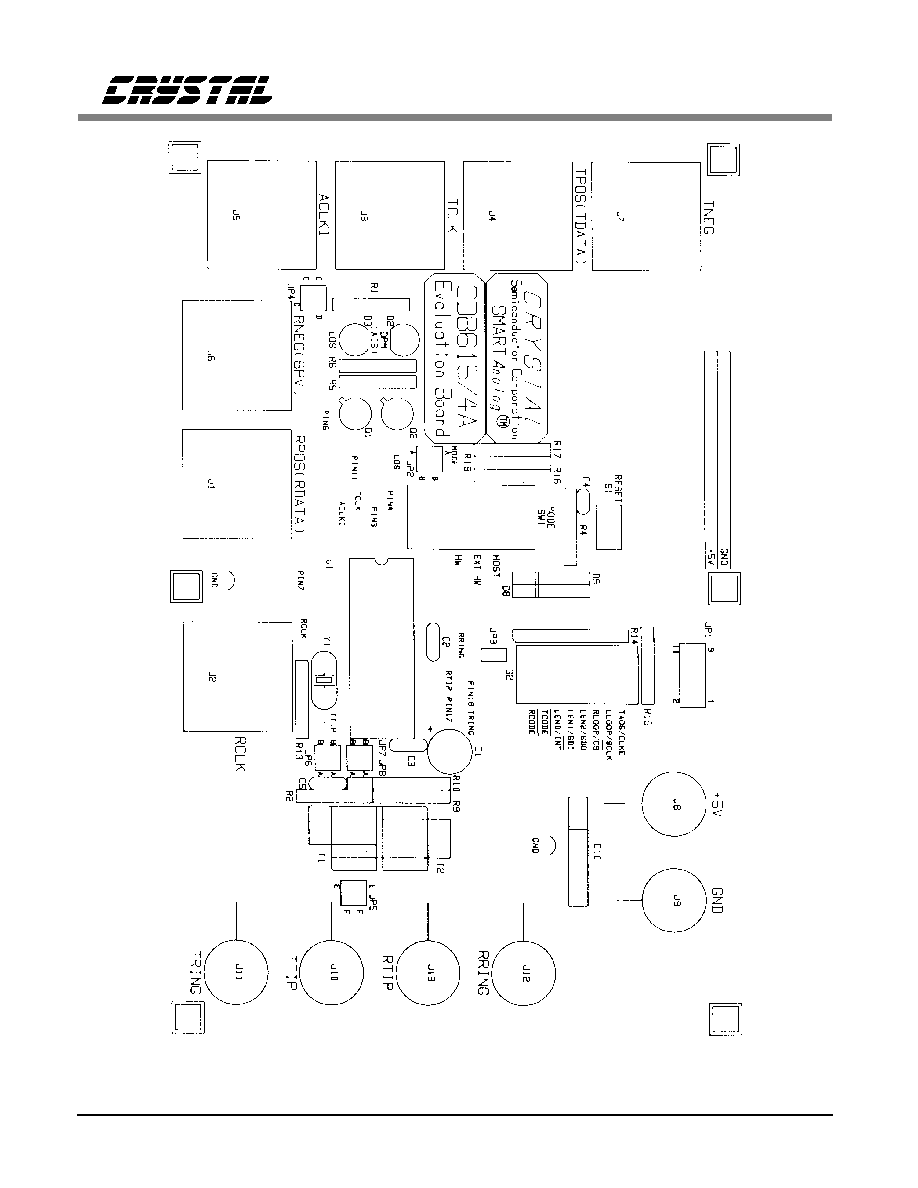
Figure 2. Silk Screen Layer (NOT TO SCALE)
LINE INTERFACE EVALUATION BOARD
42
DS40DB3

Figure 3. Top Ground Plane Layer (NOT TO SCALE)
LINE INTERFACE EVALUATION BOARD
DS40DB3
43

Figure 4. Bottom Trace Layer (NOT TO SCALE)
LINE INTERFACE EVALUATION BOARD
44
DS40DB3

∑ Notes ∑

∑ Notes ∑

∑ Notes ∑

Smart
Analog
TM
is a Trademark of Crystal Semiconductor Corporation