 | –≠–ª–µ–∫—Ç—Ä–æ–Ω–Ω—ã–π –∫–æ–º–ø–æ–Ω–µ–Ω—Ç: CS61884 | –°–∫–∞—á–∞—Ç—å:  PDF PDF  ZIP ZIP |
Preliminary Product Information
This document contains information for a new product.
Cirrus Logic reserves the right to modify this product without notice.
1
Copyright
© Cirrus Logic, Inc. 2002
(All Rights Reserved)
P.O. Box 17847, Austin, Texas 78760
(512) 445 7222 FAX: (512) 445 7581
http://www.cirrus.com
CS61884
Octal T1/E1/J1 Line Interface Unit
Features
Industry Standard Footprint
Octal E1/T1/J1 Short-haul Line Interface Unit
Low Power
No External Component Changes for
100
/120 /75 Operation
Pulse Shapes can be customized by the user
Internal AMI, B8ZS, or HDB3 Encoding/Decoding
LOS Detection per T1.231, ITU G.775, ETSI 300-233
G.772 Non-Intrusive Monitoring
G.703 BITS Clock Recovery
Crystal-less Jitter Attenuation
Serial/Parallel Microprocessor Control Interfaces
Transmitter Short Circuit Current Limiter (<50mA)
TX Drivers with Fast High-Z and Power Down
JTAG Boundary Scan compliant to IEEE 1149.1
144-Pin LQFP or 160-Pin BGA Package
ORDERING INFORMATION
CS61884-IQ
144-pin LQFP
CS61884-IB
160-pin FBGA
Description
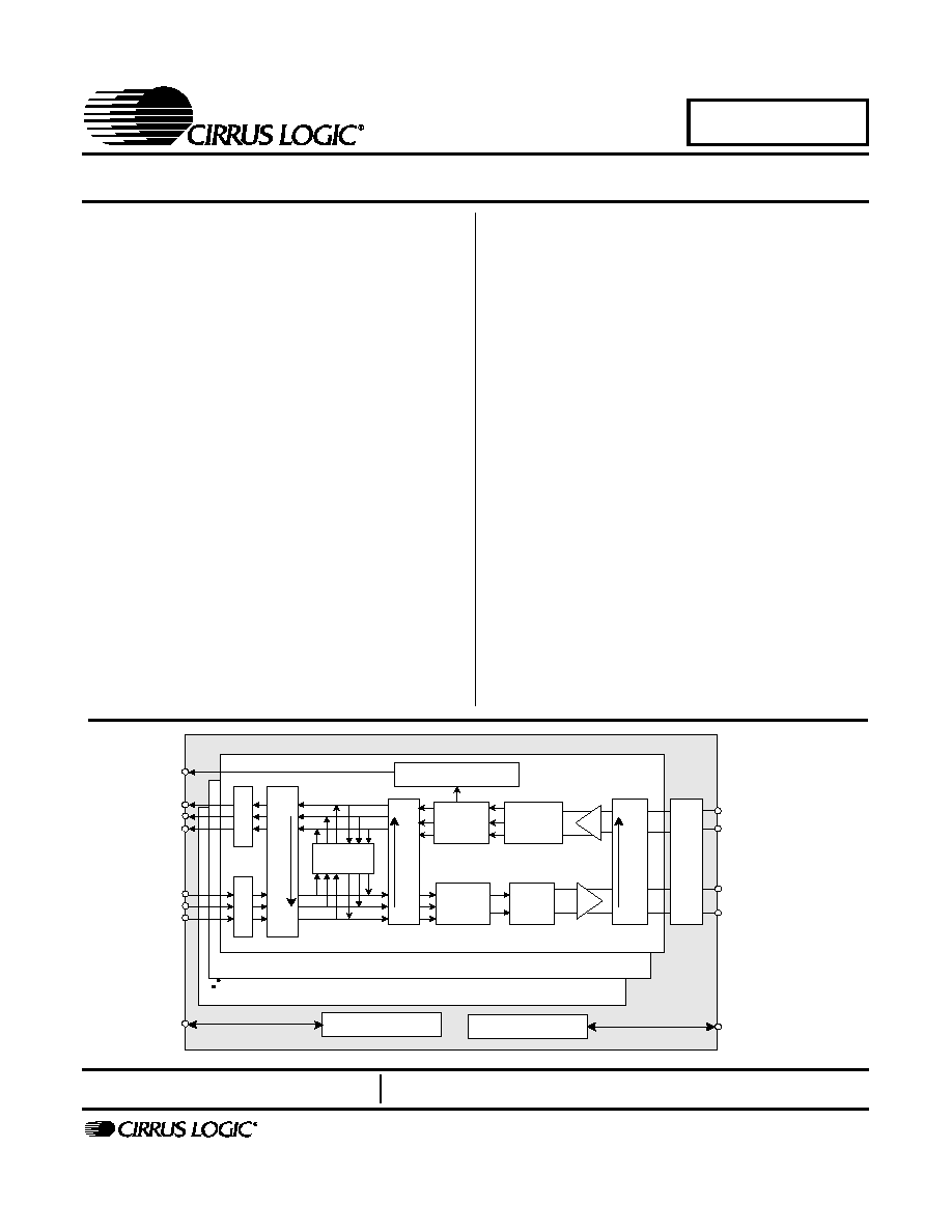
The CS61884 is a full-featured Octal E1/T1/J1 short-
haul LIU that supports both 1.544 Mbps or 2.048 Mbps
data transmission. Each channel provides crystal-less
jitter attenuation that complies with the most stringent
standards.
Each
channel
also
provides
internal
AMI/B8ZS/HDB3 encoding/decoding. To support en-
hanced system diagnostics, channel zero can be
configured for G.772 non-intrusive monitoring of any of
the other 7 channels' receive or transmit paths.
The CS61884 makes use of ultra low power matched im-
pedance transmitters and receivers to reduce power
beyond that achieved by traditional driver designs. By
achieving a more precise line match, this technique also
provides superior return loss characteristics. Additional-
ly, the internal line matching circuitry reduces the
external component count. All transmitters have controls
for independent power down and High-Z.
Each receiver provides reliable data recovery with over
12 dB of cable attenuation. The receiver also incorpo-
rates LOS detection compliant to the most recent
specifications.
Note: Click on any
text
in blue to go to cross-references.
RPOS
RNEG
TPOS
TNEG
TCLK
LOS
RTIP
RRING
TTIP
TRING
RCLK
000000000000000000000000000000000000000000000000000000000000000000000000
000000000000000000000000000000000000000000000000000000000000000000000000
000000000000000000000000000000000000000000000000000000000000000000000000
000000000000000000000000000000000000000000000000000000000000000000000000
000000000000000000000000000000000000000000000000000000000000000000000000
000000000000000000000000000000000000000000000000000000000000000000000000
000000000000000000000000000000000000000000000000000000000000000000000000
000000000000000000000000000000000000000000000000000000000000000000000000
000000000000000000000000000000000000000000000000000000000000000000000000
000000000000000000000000000000000000000000000000000000000000000000000000
000000000000000000000000000000000000000000000000000000000000000000000000
000000000000000000000000000000000000000000000000000000000000000000000000
0000000000000000000000000000000000000000000000000000000000000000000000000000
0000000000000000000000000000000000000000000000000000000000000000000000000000
0000000000000000000000000000000000000000000000000000000000000000000000000000
0000000000000000000000000000000000000000000000000000000000000000000000000000
0000000000000000000000000000000000000000000000000000000000000000000000000000
0000000000000000000000000000000000000000000000000000000000000000000000000000
0000000000000000000000000000000000000000000000000000000000000000000000000000
0000000000000000000000000000000000000000000000000000000000000000000000000000
0000000000000000000000000000000000000000000000000000000000000000000000000000
0000000000000000000000000000000000000000000000000000000000000000000000000000
0000000000000000000000000000000000000000000000000000000000000000000000000000
0000000000000000000000000000000000000000000000000000000000000000000000000000
0000000000000000000000000000000000000000000000000000000000000000000000000000
0000000000000000000000000000000000000000000000000000000000000000000000000000
0000000000000000000000000000000000000000000000000000000000000000000000000000
0000000000000000000000000000000000000000000000000000000000000000000000000000
0000000000000000000000000000000000000000000000000000000000000000000000000000
0000000000000000000000000000000000000000000000000000000000000000000000000000
0000000000000000000000000000000000000000000000000000000000000000000000000000
0000000000000000000000000000000000000000000000000000000000000000000000000000
0000000000000000000000000000000000000000000000000000000000000000000000000000
0000000000000000000000000000000000000000000000000000000000000000000000000000
0000000000000000000000000000000000000000000000000000000000000000000000000000
0000000000000000000000000000000000000000000000000000000000000000000000000000
0000000000000000000000000000000000000000000000000000000000000000000000000000
0000000000000000000000000000000000000000000000000000000000000000000000000000
0000000000000000000000000000000000000000000000000000000000000000000000000000
0000000000000000000000000000000000000000000000000000000000000000000000000000
0000000000000000000000000000000000000000000000000000000000000000000000000000
0000000000000000000000000000000000000000000000000000000000000000000000000000
0000000000000000000000000000000000000000000000000000000000000000000000000000
0000000000000000000000000000000000000000000000000000000000000000000000000000
0000000000000000000000000000000000000000000000000000000000000000000000000000
0000000000000000000000000000000000000000000000000000000000000000000000000000
0
1
7
JTAG Interface
R
e
mote
Loopbac
k
D
i
gi
tal
Loopbac
k
A
nal
og
Loopbac
k
D
e
c
oder
Driver
Receiver
LOS
G
.
772
Moni
tor
Transmit
Control
Pulse
Shaper
Data
Recovery
Jitter
Attenuator
Clock
Recovery
E
n
c
oder
Host Interface
JTAG
Serial
Port
Host
Serial/Parallel
Port
MAY `02
DS485PP4

CS61884
2
DS485PP4
TABLE OF CONTENTS
1. PINOUT - LQFP ........................................................................................................................................ 7
2. PINOUT - FBGA ........................................................................................................................................ 8
3. PIN DESCRIPTIONS ................................................................................................................................. 9
3.1 Power Supplies .................................................................................................................................. 9
3.2 Control .............................................................................................................................................. 10
3.3 Address Inputs/Loopbacks ............................................................................................................... 14
3.4 Cable Select ..................................................................................................................................... 15
3.5 Status ............................................................................................................................................... 15
3.6 Digital Rx/Tx Data I/O ....................................................................................................................... 16
3.7 Analog RX/TX Data I/O .................................................................................................................... 19
3.8 JTAG Test Interface ......................................................................................................................... 21
3.9 Miscellaneous ................................................................................................................................... 21
4. OPERATION ........................................................................................................................................... 22
5. POWER-UP ............................................................................................................................................. 22
6. MASTER CLOCK .................................................................................................................................... 22
7. G.772 MONITORING ............................................................................................................................... 22
8. BUILDING INTEGRATED TIMING SYSTEMS (BITS) CLOCK MODE .................................................. 23
9. TRANSMITTER ....................................................................................................................................... 24
9.1 Bipolar Mode .................................................................................................................................... 25
9.2 Unipolar Mode .................................................................................................................................. 25
9.3 RZ Mode ........................................................................................................................................... 25
9.4 Transmitter Powerdown / High-Z ...................................................................................................... 25
9.5 Transmit All Ones (TAOS) ................................................................................................................ 25
9.6 Automatic TAOS ............................................................................................................................... 26
9.7 Driver Failure Monitor ....................................................................................................................... 26
9.8 Driver Short Circuit Protection .......................................................................................................... 26
10. RECEIVER ............................................................................................................................................ 26
10.1 Bipolar Output Mode ...................................................................................................................... 26
10.2 Unipolar Output Mode .................................................................................................................... 26
10.3 RZ Output Mode ............................................................................................................................. 27
10.4 Receiver Powerdown/High-Z .......................................................................................................... 27
Contacting Cirrus Logic Support
For a complete listing of Direct Sales, Distributor, and Sales Representative contacts, visit the Cirrus Logic web site at:
http://www.cirrus.com/corporate/contacts/sales.cfm
IMPORTANT NOTICE
"Preliminary" product information describes products that are in production, but for which full characterization data is not yet available. "Advance" product infor-
mation describes products that are in development and subject to development changes. Cirrus Logic, Inc. and its subsidiaries ("Cirrus") believe that the infor-
mation contained in this document is accurate and reliable. However, the information is subject to change without notice and is provided "AS IS" without warranty
of any kind (express or implied). Customers are advised to obtain the latest version of relevant information to verify, before placing orders, that information being
relied on is current and complete. All products are sold subject to the terms and conditions of sale supplied at the time of order acknowledgment, including those
pertaining to warranty, patent infringement, and limitation of liability. No responsibility is assumed by Cirrus for the use of this information, including use of this
information as the basis for manufacture or sale of any items, or for infringement of patents or other rights of third parties. This document is the property of Cirrus
and by furnishing this information, Cirrus grants no license, express or implied under any patents, mask work rights, copyrights, trademarks, trade secrets or
other intellectual property rights. Cirrus owns the copyrights of the information contained herein and gives consent for copies to be made of the information only
for use within your organization with respect to Cirrus integrated circuits or other parts of Cirrus. This consent does not extend to other copying such as copying
for general distribution, advertising or promotional purposes, or for creating any work for resale.
An export permit needs to be obtained from the competent authorities of the Japanese Government if any of the products or technologies described in this ma-
terial and controlled under the "Foreign Exchange and Foreign Trade Law" is to be exported or taken out of Japan. An export license and/or quota needs to be
obtained from the competent authorities of the Chinese Government if any of the products or technologies described in this material is subject to the PRC Foreign
Trade Law and is to be exported or taken out of the PRC.
CERTAIN APPLICATIONS USING SEMICONDUCTOR PRODUCTS MAY INVOLVE POTENTIAL RISKS OF DEATH, PERSONAL INJURY, OR SEVERE
PROPERTY OR ENVIRONMENTAL DAMAGE ("CRITICAL APPLICATIONS"). CIRRUS PRODUCTS ARE NOT DESIGNED, AUTHORIZED, OR WARRANT-
ED TO BE SUITABLE FOR USE IN LIFE-SUPPORT DEVICES OR SYSTEMS OR OTHER CRITICAL APPLICATIONS. INCLUSION OF CIRRUS PRODUCTS
IN SUCH APPLICATIONS IS UNDERSTOOD TO BE FULLY AT THE CUSTOMER'S RISK.
Cirrus Logic, Cirrus, and the Cirrus Logic logo designs are trademarks of Cirrus Logic, Inc. All other brand and product names in this document may be trade-
marks or service marks of their respective owners.

CS61884
DS485PP4
3
10.5 Loss-of-Signal (LOS) .......................................................................................................................27
10.6 Alarm Indication Signal (AIS) ..........................................................................................................28
11. JITTER ATTENUATOR .........................................................................................................................28
12. OPERATIONAL SUMMARY ..................................................................................................................29
12.1 Loopbacks .......................................................................................................................................29
12.2 Analog Loopback ............................................................................................................................29
12.3 Digital Loopback ..............................................................................................................................30
12.4 Remote Loopback ...........................................................................................................................30
13. HOST MODE ..........................................................................................................................................32
13.1 SOFTWARE RESET .......................................................................................................................32
13.2 Serial Port Operation .......................................................................................................................32
13.3 Parallel Port Operation ....................................................................................................................33
13.4 Register Set ....................................................................................................................................34
14. REGISTER DESCRIPTIONS .................................................................................................................35
14.1 Revision/IDcode Register (00h) ......................................................................................................35
14.2 Analog Loopback Register (01h) .....................................................................................................35
14.3 Remote Loopback Register (02h) ...................................................................................................35
14.4 TAOS Enable Register (03h) ..........................................................................................................35
14.5 LOS Status Register (04h) ..............................................................................................................35
14.6 DFM Status Register (05h) .............................................................................................................35
14.7 LOS Interrupt Enable Register (06h) ...............................................................................................36
14.8 DFM Interrupt Enable Register (07h) ..............................................................................................36
14.9 LOS Interrupt Status Register (08h) ................................................................................................36
14.10 DFM Interrupt Status Register (09h) .............................................................................................36
14.11 Software Reset Register (0Ah) .....................................................................................................36
14.12 Performance Monitor Register (0Bh) ............................................................................................36
14.13 Digital Loopback Reset Register (0Ch) .........................................................................................37
14.14 LOS/AIS Mode Enable Register (0Dh) ..........................................................................................37
14.15 Automatic TAOS Register (0Eh) ...................................................................................................37
14.16 Global Control Register (0Fh) .......................................................................................................38
14.17 Line Length Channel ID Register (10h) .........................................................................................38
14.18 Line Length Data Register (11h) ...................................................................................................39
14.19 Output Disable Register (12h) .......................................................................................................39
14.20 AIS Status Register (13h) .............................................................................................................39
14.21 AIS Interrupt Enable Register (14h) ..............................................................................................39
14.22 AIS Interrupt Status Register (15h) ...............................................................................................40
14.23 AWG Broadcast Register (16h) .....................................................................................................40
14.24 AWG Phase Address Register (17h) ............................................................................................40
14.25 AWG Phase Data Register (18h) ..................................................................................................40
14.26 AWG Enable Register (19h) ..........................................................................................................40
14.27 AWG Overflow Interrupt Enable Register (1Ah) ............................................................................41
14.28 AWG Overflow Interrupt Status Register (1Bh) .............................................................................41
14.29 JA Error Interrupt Enable Register (1Ch) ......................................................................................41
14.30 JA Error Interrupt Status Register (1Dh) .......................................................................................41
14.31 Bits Clock Enable Register (1Eh) ..................................................................................................41
14.32 Reserved Register (1Fh) ...............................................................................................................41
14.33 Status Registers ............................................................................................................................42
14.33.1 Interrupt Enable Registers ...................................................................................................42
14.33.2 Interrupt Status Registers ....................................................................................................42
15. ARBITRARY WAVEFORM GENERATOR ............................................................................................43
16. JTAG SUPPORT ....................................................................................................................................45
16.1 TAP Controller .................................................................................................................................45
16.1.1 JTAG Reset ...........................................................................................................................45

CS61884
4
DS485PP4
16.1.2 Test-Logic-Reset ................................................................................................................... 45
16.1.3 Run-Test-Idle ........................................................................................................................ 45
16.1.4 Select-DR-Scan .................................................................................................................... 46
16.1.5 Capture-DR ........................................................................................................................... 46
16.1.6 Shift-DR ................................................................................................................................ 46
16.1.7 Exit1-DR ................................................................................................................................ 46
16.1.8 Pause-DR ............................................................................................................................. 46
16.1.9 Exit2-DR ................................................................................................................................ 46
16.1.10 Update-DR .......................................................................................................................... 46
16.1.11 Select-IR-Scan .................................................................................................................... 47
16.1.12 Capture-IR .......................................................................................................................... 47
16.1.13 Shift-IR ................................................................................................................................ 47
16.1.14 Exit1-IR ............................................................................................................................... 47
16.1.15 Pause-IR ............................................................................................................................. 47
16.1.16 Exit2-IR ............................................................................................................................... 47
16.1.17 Update-IR ........................................................................................................................... 47
16.2 Instruction Register (IR) ................................................................................................................. 47
16.2.1 EXTEST ................................................................................................................................ 47
16.2.2 SAMPLE/PRELOAD ............................................................................................................. 47
16.2.3 IDCODE ................................................................................................................................ 47
16.2.4 BYPASS ............................................................................................................................... 47
16.3 Device ID Register (IDR) ................................................................................................................ 48
17. BOUNDARY SCAN REGISTER (BSR) ................................................................................................ 48
18. APPLICATIONS .................................................................................................................................... 51
18.1 Transformer specifications ............................................................................................................. 53
18.2 Crystal Oscillator Specifications ..................................................................................................... 53
18.3 Designing for AT&T 62411 ............................................................................................................. 53
18.4 Line Protection ............................................................................................................................... 53
19. CHARACTERISTICS AND SPECIFICATIONS ..................................................................................... 54
19.1 Absolute Maximum Ratings ............................................................................................................ 54
19.2 Recommended Operating Conditions ............................................................................................ 54
19.3 Digital Characteristics ..................................................................................................................... 55
19.4 Transmitter Analog Characteristics ................................................................................................ 55
19.5 Receiver Analog Characteristics .................................................................................................... 56
19.6 Jitter Attenuator Characteristics ..................................................................................................... 57
19.7 Master Clock Switching Characteristics ......................................................................................... 59
19.8 Transmit Switching Characteristics ................................................................................................ 59
19.9 Receive Switching Characteristics ................................................................................................. 59
19.10 Switching Characteristics - Serial Port ......................................................................................... 61
19.11 Switching Characteristics - Parallel Port (Multiplexed Mode) ...................................................... 62
19.12 Switching Characteristics- Parallel Port (Non-multiplexed Mode) ............................................... 65
19.13 Switching Characteristics - JTAG ................................................................................................. 68
20. COMPLIANT RECOMMENDATIONS AND SPECIFICATIONS ........................................................... 69
21. FBGA PACKAGE DIMENSIONS .......................................................................................................... 70
22. LQFP PACKAGE DIMENSIONS
..................................................................................................... 71

CS61884
DS485PP4
5
LIST OF FIGURES
Figure 1. CS61884 144-Pin Outs ....................................................................................................... 7
Figure 2. CS61884 160-Ball FBGA Pin Outs .................................................................................... 8
Figure 3. G.703 BITS Clock Mode in NRZ Mode .......................................................................... 23
Figure 4. G.703 BITS Clock Mode in RZ Mode ............................................................................. 23
Figure 5. G.703 BITS Clock Mode in Remote Loopback ............................................................... 23
Figure 6. Pulse Mask at T1/J1 Interface .......................................................................................... 24
Figure 7. Pulse Mask at E1 Interface .............................................................................................. 24
Figure 8. Analog Loopback Block Diagram .................................................................................... 30
Figure 9. Analog Loopback with TAOS Block Diagram ................................................................ 30
Figure 10. Digital Loopback Block Diagram .................................................................................. 31
Figure 11. Digital Loopback with TAOS ........................................................................................ 31
Figure 12. Remote Loopback Block Diagram ................................................................................. 31
Figure 13. Serial Read/Write Format (SPOL = 0) ........................................................................... 33
Figure 14. Arbitrary Waveform UI .................................................................................................. 43
Figure 15. Test Access Port Architecture ........................................................................................ 45
Figure 16. TAP Controller State Diagram ....................................................................................... 46
Figure 17. Internal RX/TX Impedance Matching ............................................................................ 51
Figure 18. Internal TX, External RX Impedance Matching ............................................................ 52
Figure 19. Jitter Transfer Characteristic vs. G.736, TBR 12/13 & AT&T 62411 ........................... 58
Figure 20. Jitter Tolerance Characteristic vs. G.823 & AT&T 62411 ............................................ 58
Figure 21. Recovered Clock and Data Switching Characteristics ................................................... 60
Figure 22. Transmit Clock and Data Switching Characteristics ...................................................... 60
Figure 23. Signal Rise and Fall Characteristics ............................................................................... 60
Figure 24. Serial Port Read Timing Diagram .................................................................................. 61
Figure 25. Serial Port Write Timing Diagram ................................................................................. 61
Figure 26. Parallel Port Timing - Write; Intel Multiplexed Address / Data Bus Mode ................... 63
Figure 27. Parallel Mode Port Timing - Read; Intel Multiplexed Address / Data Bus Mode ........ 63
Figure 28. Parallel Port Timing - Write in Motorola Multiplexed Address / Data Bus .................. 64
Figure 29. Parallel Port Timing - Read in Motorola Multiplexed Address / Data Bus ................... 64
Figure 30. Parallel Port Timing - Write in Intel Non-Multiplexed Address / Data Bus Mode ....... 66
Figure 31. Parallel Port Timing - Read in Intel Non-Multiplexed Address / Data Bus Mode ........ 66
Figure 32. Parallel Port Timing - Write in Motorola Non-Multiplexed Address / Data Bus Mode 67
Figure 33. Parallel Port Timing - Read in Motorola Non-Multiplexed Address / Data Bus Mode . 67
Figure 34. JTAG Switching Characteristics .................................................................................... 68

CS61884
6
DS485PP4
LIST OF TABLES
Table 1. Operation Mode Selection ................................................................................................. 10
Table 2. Mux/Bits Clock Selection .................................................................................................. 11
Table 3. Cable Impedance Selection ................................................................................................ 15
Table 4. G.772 Address Selection .................................................................................................... 22
Table 5. Hardware Mode Line Length Configuration Selection ......................................................25
Table 6. Jitter Attenuator Configurations ......................................................................................... 28
Table 7. Operational Summary ........................................................................................................ 29
Table 8. Host Control Signal Descriptions ...................................................................................... 32
Table 9. Host Mode Register Set ..................................................................................................... 34
Table 10. JTAG Instructions ............................................................................................................ 47
Table 11. Boundary Scan Register ................................................................................................... 48
Table 12. Transformer Specifications .............................................................................................. 53

CS61884
DS485PP4
7
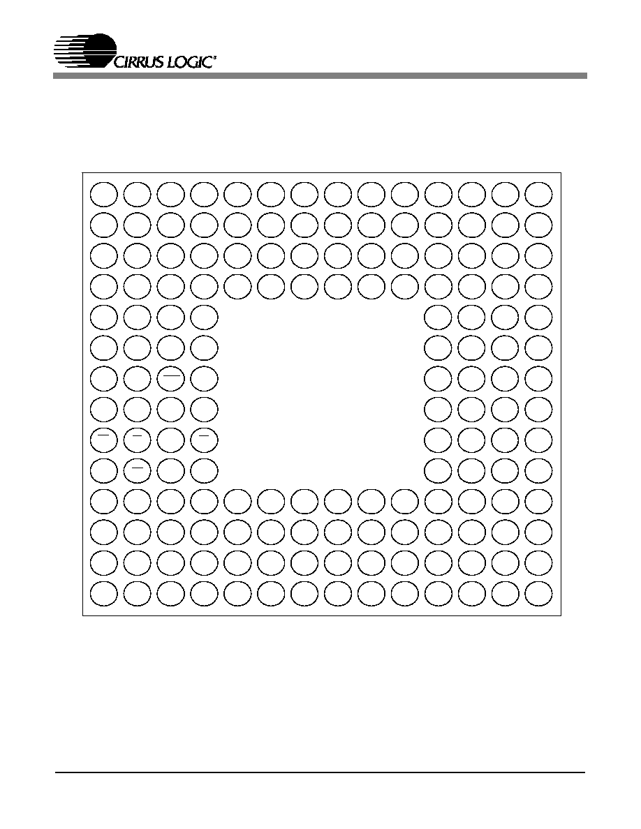
1. PINOUT - LQFP
14
4
143
14
2
14
0
13
9
13
8
13
7
13
6
13
5
14
1
13
4
13
3
13
2
13
1
13
0
12
9
128
12
7
12
6
12
5
12
4
12
3
122
121
12
0
CS6188 4
144-Pin
LQFP
37
38
39
41
42
43
44
45
46
40
47
48
49
50
51
52
53
54
55
56
57
58
59
60
61
62
63
64
65
66
67
68
69
70
71
72
108
1 0 7
1 0 6
104
1 0 3
102
101
1 0 0
99
105
98
97
96
95
94
93
9 2
91
90
8 9
88
8 7
86
85
8 4
8 3
8 2
81
8 0
79
7 8
7 7
76
75
74
7 3
119
11
8
117
11
6
11
5
11
4
11
3
11
2
11
1
11
0
10
9
1
2
3
5
6
7
8
9
1 0
4
1 1
1 2
1 3
1 4
1 5
1 6
1 7
1 8
1 9
2 0
2 1
2 2
2 3
2 4
2 5
2 6
2 7
2 8
2 9
3 0
3 1
3 2
3 3
3 4
3 5
3 6
TNE
G
7
/
UBS
7
RCLK7
RP
O
S
7
/
RDATA7
RNE
G
7
/BP
V
7
LO
S
7
RTIP
7
RRING
7
TV
+
7
TTIP
7
TRING
7
TG
ND7
RRING
6
RTIP
6
TG
ND6
TRING
6
TTIP
6
TV
+
6
RTIP
5
RRING
5
TV
+
5
TTIP
5
TRING
5
TG
ND5
RRING
4
RTIP
4
TG
ND4
TRING
4
TTIP
4
TV
+
4
CLKE
TX
O
E
LO
S
4
RNE
G
4
/BP
V
4
RP
O
S
4
/
RDATA4
RCLK4
TNE
G
4
/
UBS
4
TPOS7/TDATA7
TCLK7
LOS6
RNEG6/BPV6
RPOS6/RDATA6
RCLK6
TNEG6/UBS6
TPOS6/TDATA6
TCLK6
MCLK
MODE
A4
A3
A2
A1
A0
VCCIO
GNDIO
RV0+
RGND0
LOOP0/D0
LOOP1/D1
LOOP2/D2
LOOP3/D3
LOOP4/D4
LOOP5/D5
LOOP6/D6
LOOP7/D7
TCLK1
TPOS1/TDATA1
TNEG1/UBS1
RCLK1
RPOS1/RDATA1
RNEG1/BPV1
LOS1
TCLK0
TP
O
S
0
/
TDATA0
TNE
G
0
/
US
B0
RCLK0
RP
O
S
0
/
RDATA0
RNE
G
0
/BP
V
0
LO
S
0
M
U
X/
B
I
T
SEN
0
TV
+
0
TTIP
0
TRING
0
TG
ND0
RTIP
0
RRING
0
TG
ND1
TRING
1
TTIP
1
TV
+
1
RRING
1
RTIP
1
TV
+
2
TTIP
2
TRING
2
TG
ND2
RTIP
2
RRING
2
TG
ND3
TRING
3
TTIP
3
TV
+
3
RRING
3
RTIP
3
LO
S
3
RNE
G
3
/RBP
V
3
RP
O
S
3
/
RDATA3
RCLK3
TNE
G
3
/
UBS
3
(Top View)
TPOS4/TDATA4
TCLK4
LOS5
RNEG5/BPV5
RPOS5/RDATA5
RCLK5
TNEG5/UBS5
TPOS5/TDATA5
TCLK5
TDI
TDO
TCK
TMS
TRST
REF
CBLSEL
VCCIO
GNDIO
RV1+
RGND1
INTL/MOT/CODEN
CS/JASEL
ALE/AS/SCLK/LEN2
RD/RW/LEN1
WR/DS/SDI/LEN0
RDY/ACK/SDO
INT
TCLK2
TPOS2/TDATA2
TNEG2/UBS2
RCLK2
RPOS2/RDATA2
RNEG2/BPV2
LOS2
TCLK3
TPOS3/TDATA3
Figure 1. CS61884 144-Pin Outs
CS61884
8
DS485PP4
2. PINOUT - FBGA
1
2
3
4
5
6
7
8
9
10
11
12
13
14
CLKE
TDO
CBLSEL
REF
TPOS
5
RPOS
4
TPOS
4
RPOS
5
TPOS
2
RPOS
3
TPOS
3
RPOS
2
TTIP
5
TRING
4
TTIP
4
TRING
5
TTIP
2
TRING
3
TTIP
3
TRING
2
TGND
5
TGND
4
TGND
4
TGND
5
TGND
2
TGND
3
TGND
3
TGND
2
RRING
5
RTIP
4
RRING
4
RTIP
5
RRING
2
RTIP
3
RRING
3
RTIP
2
RRING
6
RTIP
7
RRING
7
RTIP
6
RRING
1
RTIP
0
RRING
0
RTIP
1
TGND
6
TGND
7
TGND
7
TGND
6
TGND
1
TGND
0
TGND
0
TGND
1
TTIP
6
TRING
7
TTIP
7
TRING
6
TTIP
1
TRING
0
TTIP
0
TRING
1
TVCC
6
TVCC
7
TVCC
7
TVCC
6
TVCC
1
TVCC
0
TVCC
0
TVCC
1
LOS
7
A4
GNDIO
LOOP
3
LOS
0
RGND
0
TNEG
6
RNEG
7
TNEG
7
RNEG
6
TNEG
1
RNEG
0
TNEG
0
RNEG
1
LOS
6
A3
A0
LOOP
4
LOS
1
LOOP
1
TPOS
6
RPOS
7
TPOS
7
RPOS
6
TPOS
1
RPOS
0
TPOS
0
RPOS
1
MODE
A2
LOOP
0
LOOP
5
MUX
LOOP
2
TCLK
6
RCLK
7
TCLK
7
RCLK
6
TCLK
1
RCLK
0
TCLK
0
RCLK
1
MCLK
A1
VCCIO
LOOP
6
LOOP
7
RV0+
1
2
3
4
5
6
7
8
9
10
11
12
13
14
A
B
C
D
E
F
G
H
J
K
L
M
N
P
A
B
C
D
E
F
G
H
J
K
L
M
N
P
CS61884
160 FBGA
(Bottom View)
LOS
4
TMS
GNDIO
RGND
1
CS
LOS
3
TVCC
5
TVCC
4
TVCC
4
TVCC
5
TVCC
2
TVCC
3
TVCC
3
TVCC
2
RD
TXOE
TCK
VCCIO
RV1+
WR
RDY
TCLK
5
RCLK
4
TCLK
4
RCLK
5
TCLK
2
RCLK
3
TCLK
3
RCLK
2
INT
LOS
5
TDI
TRST
INTL
ALE
LOS
2
TNEG
5
RNEG
4
TNEG
4
RNEG
5
TNEG
2
RNEG
3
TNEG
3
RNEG
2
Figure 2. CS61884 160-Ball FBGA Pin Outs

CS61884
DS485PP4
9
3. PIN DESCRIPTIONS
3.1 Power Supplies
SYMBOL
LQFP
FBGA
TYPE
DESCRIPTION
VCCIO
17
92
G1
G14
Power Supply, Digital Interface: Power supply for digital
interface pins; typically 3.3V.
GNDIO
18
91
G4
G11
Ground, Digital Interface:
Power supply ground for the digital interface; typically 0 Volts
RV0+
RV1+
19
90
H1
H14
Power Supply, Core Circuitry: Power supply for all sub-cir-
cuits except the transmit driver; typically +3.3 Volts
RGND0
RGND1
20
89
H4
H11
Ground, Core Circuitry:
Ground for sub-circuits except the TX driver; typically 0 Volts
TV+0
44
N4, P4
Power Supply, Transmit Driver 0
Power supply for transmit driver 0; typically +3.3 Volts
TGND0
47
N6, P6
Ground, Transmit Driver 0
Power supply ground for transmit driver 0; typically 0 Volts
TV+1
53
L4, M4
Power Supply, Transmit Driver 1
TGND1
50
L6, M6
Ground, Transmit Driver 1
TV+2
56
L11
M11
Power Supply, Transmit Driver 2
TGND2
59
L9, M9
Ground, Transmit Driver 2
TV+3
65
N11
P11
Power Supply, Transmit Driver 3
TGND3
62
N9, P9
Ground, Transmit Driver 3
TV+4
116
A11
B11
Power Supply, Transmit Driver 4
TGND4
119
A9, B9
Ground, Transmit Driver 4
TV+5
125
C11
D11
Power Supply, Transmit Driver 5
TGND5
122
C9,
D9
Ground, Transmit Driver 5
TV+6
128
C4,
D4
Power Supply, Transmit Driver 6
TGND6
131
C6,
D6
Ground, Transmit Driver 6
TV+7
137
A4, B4
Power Supply, Transmit Driver 7
TGND7
134
A6, B6
Ground, Transmit Driver 7

CS61884
10
DS485PP4
3.2 Control
SYMBOL
LQFP
FBGA
TYPE
DESCRIPTION
MCLK
10
E1
I
Master Clock Input
This pin is a free running reference clock that should be
either 1.544 MHz for T1/J1 or 2.048 MHz for E1 operation.
This timing reference is used as follows:
- Timing reference for the clock recovery and jitter attenua-
tion circuitry.
- RCLK reference during Loss of Signal (LOS) conditions
- Transmit clock reference during Transmit all Ones (TAOS)
condition
- Wait state timing for microprocessor interface
- When this pin is held "High", the PLL clock recovery cir-
cuit is disabled. In this mode, the CS61884 receivers
function as simple data slicers.
- When this pin is held "Low", the receiver paths are pow-
ered down and the output pins RCLK, RPOS, and RNEG
are High-Z.
MODE
11
E2
I
Mode Select
This pin is used to select whether the CS61884 operates in
Serial host, Parallel host or Hardware mode.
Host Mode - The CS61884 is controlled through either a
serial or a parallel microprocessor interface (Refer to
HOST
MODE
(See Section 13 on page 32).
Hardware Mode - The microprocessor interface is disabled
and the device control/status are provided through the pins
on the device.
NOTE: For serial host mode connect this pin to a resistor
divider consisting of two 10K
resistors between
VCCIO and GNDIO.
Table 1. Operation Mode Selection
Pin State
OPERATING Mode
LOW
Hardware Mode
HIGH
Parallel Host Mode
VCCIO/2
Serial Host Mode
CS61884
DS485PP4
11
MUX/BITSEN0
43
K2
I
Multiplexed Interface/Bits Clock Select
Host Mode -This pin configures the microprocessor inter-
face for multiplexed or non-multiplexed operation.
Hardware mode - This pin is used to enable channel 0 as
a G.703 BITS Clock recovery channel (Refer to
BUILDING
INTEGRATED TIMING SYSTEMS (BITS) CLOCK MODE
(See Section 8 on page 23). Channel 1 through 7 are not
affected by this pin during hardware mode. During host
mode the G.703 BITS Clock recovery function is enabled by
the
Bits Clock Enable Register (1Eh)
(See Section 14.31
on page 41).
NOTE: The MUX pin only controls the BITS Clock function in
Hardware Mode
INT
82
K13
O
Interrupt Output
This active low output signals the host processor when one
of the CS61884's internal status register bits has changed
state. When the status register is read, the interrupt is
cleared. The various status changes that would force INT
active are maskable via internal interrupt enable registers.
NOTE: This pin is an open drain output and requires a 10 k
pull-up resistor.
RDY/ACK/SDO
83
K14
O
Data Transfer Acknowledge/Ready/Serial Data Output
Intel Parallel Host Mode - During a read or write register
access, RDY is asserted "Low" to acknowledge that the de-
vice has been accessed. An asserted "High" acknowledges
that data has been written or read. Upon completion of the
bus cycle, this pin High-Z.
Motorola Parallel Host Mode - During a data bus read
operation this pin "ACK" is asserted "High" to indicate that
data on the bus is valid. An asserted "Low" on this pin dur-
ing a write operation acknowledges that a data transfer to
the addressed register has been accepted. Upon comple-
tion of the bus cycle, this pin High-Z.
NOTE: Wait state generation via RDY/ACK is disabled in
RZ mode (No Clock Recovery).
Serial Host Mode - When the microprocessor interface is
configured for serial bus operation, "SDO" is used as a seri-
al data output. This pin is forced into a high impedance
state during a serial write access. The CLKE pin controls
whether SDO is valid on the rising or falling edge of SCLK.
Upon completion of the bus cycle, this pin High-Z.
Hardware Mode - This pin is not used and should be left
open.
SYMBOL
LQFP
FBGA
TYPE
DESCRIPTION
Table 2. Mux/Bits Clock Selection
Pin State
Parallel Host Mode
Hardware Mode
HIGH
multiplexed
BITS Clock ON
LOW
non multiplexed
BITS Clock OFF
CS61884
12
DS485PP4
WR/DS/SDI/LEN0
84
J14
I
Data Strobe/ Write Enable/Serial Data/Line Length Input
Intel Parallel Host Mode - This pin "WR" functions as a
write enable.
Motorola Parallel Host Mode - This pin "DS" functions as
a data strobe input.
Serial Host Mode - This pin "SDI" functions as the serial
data input.
Hardware Mode - As LEN0, this pin controls the transmit
pulse shapes for both E1 and T1/J1 modes. This pin also
selects which mode is used E1 or T1/J1 (Refer to
Table 5
on page 25
).
RD/RW/LEN1
85
J13
I
Read/Write/ Read Enable/Line Length Input
Intel Parallel Host Mode - This pin "RD" functions as a
read enable.
Motorola Parallel Host Mode - This pin "R/W" functions as
the read/write input signal.
Hardware Mode - As LEN1, this pin controls the transmit
pulse shapes for both E1 and T1/J1 modes. This pin also
selects which mode is used E1 or T1/J1 (Refer to
Table 5
on page 25
).
ALE/AS/SCLK/LEN2
86
J12
I
Address Latch Enable/Serial Clock/Address Strobe/Line
Length Input
Intel Parallel Host Mode - This pin "ALE" functions as the
Address Latch Enable when configured for multiplexed ad-
dress/data operation.
Motorola Parallel Host Mode - This pin "AS" functions as
the active "low" address strobe when configured for multi-
plexed address/data operation.
Serial Host Mode - This pin "SCLK" is the serial clock
used for data I/O on SDI and SDO.
Hardware Mode - As LEN2, this pin controls the transmit
pulse shapes for both E1 and T1/J1 modes. This pin also
selects which mode is used E1 or T1/J1 (Refer to
Table 5
on page 25
).
CS/JASEL
87
J11
I
Chip Select Input/Jitter Attenuator Select
Host Mode - This active low input is used to enable ac-
cesses to the microprocessor interface in either serial or
parallel mode.
Hardware Mode - This pin controls the position of the Jitter
Attenuator.
SYMBOL
LQFP
FBGA
TYPE
DESCRIPTION
Pin State
Jitter Attenuation Position
LOW
Transmit Path
HIGH
Receive Path
OPEN
Disabled
CS61884
DS485PP4
13
INTL/MOT/CODEN
88
H12
I
Motorola/Intel/Coder Mode Select Input
Parallel Host Mode - When this pin is "Low" the micropro-
cessor interface is configured for operation with Motorola
processors. When this pin is "High" the microprocessor in-
terface is configured for operation with Intel processors.
Hardware Mode - When the CS61884 is configured for uni-
polar operation, this pin, CODEN, configures the line
encoding/decoding function. When CODEN is low,
B8ZS/HDB3 encoders/decoders are enabled for T1/J1 or
E1 operation respectively. When CODEN is high, AMI en-
coding/decoding is activated. This is done for all eight
channels.
TXOE
114
E14
I
Transmitter Output Enable
Host mode - Operates the same as in hardware mode. In-
dividual drivers can be set to a high impedance state via
the
Output Disable Register (12h)
(See Section 14.19 on
page 39).
Hardware Mode - When TXOE pin is asserted Low, all the
TX drivers are forced into a high impedance state. All other
internal circuitry remains active.
CLKE
115
E13
I
Clock Edge Select
In clock/data recovery mode, setting CLKE "high" will cause
RPOS/RNEG to be valid on the falling edge of RCLK and
SDO to be valid on the rising edge of SCLK. When CLKE is
set "low", RPOS/RNEG is valid on the rising edge of RCLK,
and SDO is valid on the falling edge of SCLK. When the
part is operated in data recovery mode, the RPOS/RNEG
output polarity is active "high" when CLKE is set "high" and
active "low" when CLKE is set "low".
SYMBOL
LQFP
FBGA
TYPE
DESCRIPTION
CS61884
14
DS485PP4
3.3 Address Inputs/Loopbacks
SYMBOL
LQFP
FBGA
TYPE
DESCRIPTION
A4
12
F4
I
Address Selector Input
Parallel Host Mode - During non-multiplexed parallel host
mode operation, this pin function as the address 4 input for
the parallel interface.
Hardware Mode - The A4 pin must be tied low at all times.
A3
A2
A1
A0
13
14
15
16
F3
F2
F1
G3
I
I
I
I
Non-Intrusive Monitoring/Address Selector Inputs
Parallel Host Mode - During non-multiplexed parallel host
mode operation, these pins function as address A[3:0] in-
puts for the parallel interface.
Hardware Mode - The A[3:0] pins are used for port selec-
tion during non-intrusive monitoring. In non-intrusive
monitoring mode, receiver 0's input is internally connected
to the transmit or receive ports on one of the other 7 chan-
nels. The recovered clock and data from the selected port
are output on RPOS0/RNEG0 and RCLK0. Additionally, the
data from the selected port can be output on
TTIP0/TRING0 by activating the remote loopback function
for channel 0 (Refer to
Performance Monitor Register
(0Bh)
(See Section 14.12 on page 36).
LOOP0/D0
LOOP1/D1
LOOP2/D2
LOOP3/D3
LOOP4/D4
LOOP5/D5
LOOP6/D6
LOOP7/D7
21
22
23
24
25
26
27
28
G2
H3
H2
J4
J3
J2
J1
K1
I/O
I/O
I/O
I/O
I/O
I/O
I/O
I/O
Loopback Mode Selector/Parallel Data Input/Output
Parallel Host Mode - In non-multiplexed microprocessor in-
terface mode, these pins function as the bi-directional 8-bit
data port. When operating in multiplexed microprocessor in-
terface mode, these pins function as the address and data
inputs/outputs.
Hardware Mode
- No Loopback - The CS61884 is in a normal operating
state when LOOP is left open (unconnected) or tied to
VCCIO/2.
- Local Loopback - When LOOP is tied High, data transmit-
ted on TTIP and TRING is looped back into the analog
input of the corresponding channel's receiver and output on
RPOS and RNEG. Input Data present on RTIP and RRING
is ignored.
- Remote Loopback - When LOOP is tied Low the recov-
ered clock and data received on RTIP and RRING is looped
back for transmission on TTIP and TRING. Data on TPOS
and TNEG is ignored.

CS61884
DS485PP4
15
3.4 Cable Select
3.5
Status
SYMBOL
LQFP
FBGA
TYPE
DESCRIPTION
CBLSEL
93
G13
I
Cable Impedance Select
Host Mode - The input voltage to this pin does not effect
normal operation.
Hardware Mode - This pin is used in combination with the
LEN control pins (Refer to
Table 5, "Hardware Mode Line
Length Configuration Selection," on page 25
) to set the line
impedance for all eight receivers and transmitters. This pin
also selects whether or not all eight receivers use an inter-
nal or external line matching network (Refer to the Table
below for proper settings).
NOTE: Refer to
Figure 17 on page 51
and
Figure 18 on
page 52
for appropriate external line matching com-
ponents. All transmitters use internal matching net-
works.
Table 3. Cable Impedance Selection
E1/T1/J1
CBLSEL
Transmitters
Receivers
T1/J1
No Connect
100
Internal
Internal
T1/J1
HIGH
100
Internal
Internal
T1/J1
LOW
100
Internal
External
E1
No Connect
120
Internal
Inter or Ext
E1
HIGH
75
Internal
Internal
E1
LOW
75
Internal
External
SYMBOL
LQFP
FBGA
TYPE
DESCRIPTION
LOS0
LOS1
LOS2
LOS3
LOS4
LOS5
LOS6
LOS7
42
35
75
68
113
106
3
140
K4
K3
K12
K11
E11
E12
E3
E4
O
O
O
O
O
O
O
O
Loss of Signal Output
The LOS output pins can be configured to indicate a loss of
signal (LOS) state that is compliant to either T1.231, ITU
G.775 or ETSI 300 233. These pins are asserted "High" to
indicate LOS. The LOS output returns low when an input
signal is present for the time period dictated by the associ-
ated specification (Refer to
Loss-of-Signal (LOS)
(See
Section 10.5 on page 27)).
CS61884
16
DS485PP4
3.6 Digital Rx/Tx Data I/O
SYMBOL
LQFP
FBGA
TYPE
DESCRIPTION
TCLK0
36
N1
I
Transmit Clock Input Port 0
- When TCLK is active, the TPOS and TNEG pins function
as NRZ inputs that are sampled on the falling edge of
TCLK.
- If MCLK is active, TAOS will be generated when TCLK is
held High for 16 MCLK cycles.
NOTE: MCLK is used as the timing reference during TAOS
and must have the appropriate stability.
- If TCLK is held High in the absence of MCLK, the TPOS
and TNEG inputs function as RZ inputs. In this mode, the
transmit pulse width is set by the pulse-width of the signal
input on TPOS and TNEG. To enter this mode, TCLK must
be held high for at least 12
µS.
- If TCLK is held Low, the output drivers enter a low-power,
high impedance state.
TPOS0/TDATA0
TNEG0/UBS
37
38
N2
N3
I
I
Transmit Positive Pulse/Transmit Data Input Port 0
Transmit Negative Pulse/Unipolar-Bipolar Select Port 0
The function of the TPOS/TDATA and TNEG/UBS inputs
are determined by whether Unipolar, Bipolar or RZ input
mode has been selected.
Bipolar Mode - In this mode, NRZ data on TPOS and
TNEG are sampled on the falling edge of TCLK and trans-
mitted onto the line at TTIP and TRING respectively. A
"High" input on TPOS results in transmission of a positive
pulse; a "High" input on TNEG results in a transmission of a
negative pulse. The translation of TPOS/TNEG inputs to
TTIP/TRING outputs is as follows:
Unipolar mode - Unipolar mode is activated by holding
TNEG/UBS "High" for more than 16 TCLK cycles, when
MCLK is present. The falling edge of TCLK samples a uni-
polar data steam on TPOS/TDATA.
RZ Mode - To activate RZ mode tie TCLK "High" with the
absence of MCLK. In this mode, the duty cycle of the
TPOS and TNEG inputs determine the pulse width of the
output signal on TTIP and TRING.
TPOS
TNEG
OUTPUT
0
0
Space
1
0
Positive Mark
0
1
Negative Mark
1
1
Space

CS61884
DS485PP4
17
RCLK0
39
P1
O
Receive Clock Output Port 0
- When MCLK is active, this pin outputs the recovered clock
from the signal input on RTIP and RRING. In the event of
LOS, the RCLK output transitions from the recovered clock
to MCLK.
- If MCLK is held "High", the clock recovery circuitry is dis-
abled and the RCLK output is driven by the XOR of RNEG
and RPOS.
- If MCLK is held "Low", this output is in a high-impedance
state.
RPOS0/RDATA0
RNEG0/BPV0
40
41
P2
P3
O
O
Receive Positive Pulse/ Receive Data Output Port 0
Receive Negative Pulse/Bipolar Violation Output Port 0
The function of the RPOS/RDATA and RNEG/BPV outputs
are determined by whether Unipolar, Bipolar, or RZ input
mode has been selected. During LOS, the RPOS/RNEG
outputs will remain active.
NOTE: The RPOS/RNEG outputs can be High-Z by holding
MCLK Low.
Bipolar Output Mode - When configured for Bipolar opera-
tion, NRZ Data is recovered from RTIP/RRING and output
on RPOS/RNEG. A high signal on RPOS or RNEG corre-
spond to the receipt of a positive or negative pulse on
RTIP/RRING respectively. The RPOS/RNEG outputs are
valid on the falling or rising edge of RCLK as configured by
CLKE.
Unipolar Output Mode - When unipolar mode is activated,
the recovered data is output on RDATA. The decoder sig-
nals bipolar Violations on the RNEG/BPV pin.
RZ Output Mode - In this mode, the RPOS/RNEG pins
output RZ data recovered by slicing the signal present on
RTIP/RRING. A positive pulse on RTIP with respect to
RRING generates a logic 1 on RPOS; a positive pulse on
RRING with respect to RTIP generates a logic 1 on RNEG.
The polarity of the output on RPOS/RNEG is selectable us-
ing the CLKE pin. In this mode, external circuitry is used to
recover clock from the received signal.
TCLK1
29
L1
I
Transmit Clock Input Port 1
TPOS1/TDATA1
30
L2
I
Transmit Positive Pulse/Transmit Data Input Port 1
TNEG1/UBS1
31
L3
I
Transmit Negative Pulse/Unipolar-Bipolar Select Port 1
RCLK1
32
M1
O
Receive Clock Output Port 1
RPOS1/RDATA1
33
M2
O
Receive Positive Pulse/ Receive Data Output Port 1
RNEG1/BPV1
34
M3
O
Receive Negative Pulse/Bipolar Violation Output Port 1
TCLK2
81
L14
I
Transmit Clock Input Port 2
TPOS2/TDATA2
80
L13
I
Transmit Positive Pulse/Transmit Data Input Port 2
TNEG2/UBS2
79
L12
I
Transmit Negative Pulse/Unipolar-Bipolar Select Port 2
SYMBOL
LQFP
FBGA
TYPE
DESCRIPTION

CS61884
18
DS485PP4
RCLK2
78
M14
O
Receive Clock Output Port 2
RPOS2/RDATA2
77
M13
O
Receive Positive Pulse/ Receive Data Output Port 2
RNEG2/BPV2
76
M12
O
Receive Negative Pulse/Bipolar Violation Output Port 2
TCLK3
74
N14
I
Transmit Clock Input Port 3
TPOS3/TDATA3
73
N13
I
Transmit Positive Pulse/Transmit Data Input Port 3
TNEG3/UBS3
72
N12
I
Transmit Negative Pulse/Unipolar-Bipolar Select Port 3
RCLK3
71
P14
O
Receive Clock Output Port 3
RPOS3/RDATA3
70
P13
O
Receive Positive Pulse/ Receive Data Output Port 3
RNEG3/BPV3
69
P12
O
Receive Negative Pulse/Bipolar Violation Output Port 3
TCLK4
107
B14
I
Transmit Clock Input Port 4
TPOS4/TDATA4
108
B13
I
Transmit Positive Pulse/Transmit Data Input Port 4
TNEG4/UBS4
109
B12
I
Transmit Negative Pulse/Unipolar-Bipolar Select Port 4
RCLK4
110
A14
O
Receive Clock Output Port 4
RPOS4/RDATA4
111
A13
O
Receive Positive Pulse/ Receive Data Output Port 4
RNEG4/BPV4
112
A12
O
Receive Negative Pulse/Bipolar Violation Output Port 4
TCLK5
100
D14
I
Transmit Clock Input Port 5
TPOS5/TDATA5
101
D13
I
Transmit Positive Pulse/Transmit Data Input Port 5
TNEG5/UBS5
102
D12
I
Transmit Negative Pulse/Unipolar-Bipolar Select Port 5
RCLK5
103
C14
O
Receive Clock Output Port 5
RPOS5/RDATA5
104
C13
O
Receive Positive Pulse/ Receive Data Output Port 5
RNEG5/BPV5
105
C12
O
Receive Negative Pulse/Bipolar Violation Output Port 5
TCLK6
9
D1
I
Transmit Clock Input Port 6
TPOS6/TDATA6
8
D2
I
Transmit Positive Pulse/Transmit Data Input Port 6
TNEG6/UBS6
7
D3
I
Transmit Negative Pulse/Unipolar-Bipolar Select Port 6
RCLK6
6
C1
O
Receive Clock Output Port 6
RPOS6/RDATA6
5
C2
O
Receive Positive Pulse/ Receive Data Output Port 6
RNEG6/BPV6
4
C3
O
Receive Negative Pulse/Bipolar Violation Output Port 6
TCLK7
2
B1
I
Transmit Clock Input Port 7
TPOS7/TDATA7
1
B2
I
Transmit Positive Pulse/Transmit Data Input Port 7
TNEG7/UBS7
144
B3
I
Transmit Negative Pulse/Unipolar-Bipolar Select Port 7
SYMBOL
LQFP
FBGA
TYPE
DESCRIPTION
CS61884
DS485PP4
19
3.7 Analog RX/TX Data I/O
RCLK7
143
A1
O
Receive Clock Output Port 7
RPOS7/RDATA7
142
A2
O
Receive Positive Pulse/ Receive Data Output Port 7
RNEG7/BPV7
141
A3
O
Receive Negative Pulse/Bipolar Violation Output Port 7
SYMBOL
LQFP
FBGA
TYPE
DESCRIPTION
SYMBOL
LQFP
FBGA
TYPE
DESCRIPTION
TTIP0
TRING0
45
46
N5
P5
O
O
Transmit Tip Output Port 0
Transmit Ring Output Port 0
TTIP and TRING pins are the differential outputs of the
transmit driver. The driver internally matches impedances
for E1 75
, E1 120 and T1/J1 100 lines requiring only
a 1:2 transformer. The CBLSEL pin is used to select the
appropriate line matching impedance only in "Hardware"
mode. In host mode, the appropriate line matching imped-
ance is selected by the
Line Length Data Register (11h)
(See Section 14.18 on page 39).
NOTE: TTIP and TRING are forced to a high impedance state
when the TCLK pin is "Low" for over 12
µS or the
TXOE pin is forced "Low".
RTIP0
RRING0
48
49
P7
N7
I
I
Receive Tip Input Port 0
Receive Ring Input Port 0
RTIP and RRING are the differential line inputs to the re-
ceiver. The receiver uses either Internal Line Impedance or
External Line Impedance modes to match the line imped-
ances for E1 75
, E1 120 or T1/J1 100 modes.
Internal Line Impedance Mode - The receiver uses the
same external resistors to match the line impedance (Refer
to
Figure 17 on page 51
).
External Line Impedance Mode - The receiver uses differ-
ent external resistors to match the line impedance (Refer to
Figure 18 on page 52
).
- In host mode, the appropriate line impedance is selected
by the
Line Length Data Register (11h)
(See Section
14.18 on page 39).
- In hardware mode, the CBLSEL pin in combination with
the LEN pins select the appropriate line impedance. (Refer
to
Table 3 on page 15
for proper line impedance settings).
NOTE: Data and clock recovered from the signal input on
these pins are output via RCLK, RPOS, and RNEG.
TTIP1
52
L5
O
Transmit Tip Output Port 1
TRING1
51
M5
O
Transmit Ring Output Port 1
RTIP1
55
M7
I
Receive Tip Input Port 1
RRING1
54
L7
I
Receive Ring Input Port 1

CS61884
20
DS485PP4
TTIP2
57
L10
O
Transmit Tip Output Port 2
TRING2
58
M10
O
Transmit Ring Output Port 2
RTIP2
60
M8
I
Receive Tip Input Port 2
RRING2
61
L8
I
Receive Ring Input Port 2
TTIP3
64
N10
O
Transmit Tip Output Port 3
TRING3
63
P10
O
Transmit Ring Output Port 3
RTIP3
67
P8
I
Receive Tip Input Port 3
RRING3
66
N8
I
Receive Ring Input Port 3
TTIP4
117
B10
O
Transmit Tip Output Port 4
TRING4
118
A10
O
Transmit Ring Output Port 4
RTIP4
120
A8
I
Receive Tip Input Port 4
RRING4
121
B8
I
Receive Ring Input Port 4
TTIP5
124
D10
O
Transmit Tip Output Port 5
TRING5
123
C10
O
Transmit Ring Output Port 5
RTIP5
127
C8
I
Receive Tip Input Port 5
RRING5
126
D8
I
Receive Ring Input Port 5
TTIP6
129
D5
O
Transmit Tip Output Port 6
TRING6
130
C5
O
Transmit Ring Output Port 6
RTIP6
132
C7
I
Receive Tip Input Port 6
RRING6
133
D7
I
Receive Ring Input Port 6
TTIP7
136
B5
O
Transmit Tip Output Port 7
TRING7
135
A5
O
Transmit Ring Output Port 7
RTIP7
139
A7
I
Receive Tip Input Port 7
RRING7
138
B7
I
Receive Ring Input Port 7
SYMBOL
LQFP
FBGA
TYPE
DESCRIPTION

CS61884
DS485PP4
21
3.8 JTAG Test Interface
3.9 Miscellaneous
SYMBOL
LQFP
FBGA
TYPE
DESCRIPTION
TRST
95
G12
I
JTAG Reset
This active Low input resets the JTAG controller. This input
is pulled up internally and may be left as a NC when not
used.
TMS
96
F11
I
JTAG Test Mode Select Input
This input enables the JTAG serial port when active High.
This input is sampled on the rising edge of TCK. This input
is pulled up internally and may be left as a NC when not
used.
TCK
97
F14
I
JTAG Test Clock
Data on TDI is valid on the rising edge of TCK. Data on
TDO is valid on the falling edge of TCK. When TCK is
stopped high or low, the contents of all JTAG registers re-
main unchanged. Tie pin low through a 10 K
resistor
when not used.
TDO
98
F13
O
JTAG Test Data Output
JTAG test data is shifted out of the device on this pin. Data
is output on the falling edge of TCK. Leave as NC when not
used.
TDI
99
F12
I
JTAG Test Data Input
JTAG test data is shifted into the device using this pin. The
pin is sampled on the rising edge of TCK. TDI is pulled up
internally and may be left as a NC when not used.
SYMBOL
LQFP
FBGA
TYPE
DESCRIPTION
REF
94
H13
I
Reference Input
This pin must be tied to ground through 13.3 K
1% resis-
tor. This pin is used to set the internal current level.

CS61884
22
DS485PP4
4. OPERATION
The CS61884 is a full featured line interface unit
for up to eight E1/T1/J1 lines. The device provides
an interface to twisted pair or co-axial media. A
matched impedance technique is employed that re-
duces power and eliminates the need for matching
resistors. As a result, the device can interface di-
rectly to the line through a transformer without the
need for matching resistors on the transmit side.
The receive side uses the same resistor values for
all E1/T1/J1 settings.
5. POWER-UP
On power-up, the device is held in a static state un-
til the power supply achieves approximately 70%
of the power supply voltage. Once the power sup-
ply threshold is passed, the analog circuitry is cali-
brated, the control registers are reset to their default
settings, and the various internal state machines are
reset. The reset/calibration process completes in
about 30 ms.
6. MASTER CLOCK
The CS61884 requires a 2.048 MHz or 1.544 MHz
reference clock with a minimum accuracy of ±100
ppm. This clock may be supplied from internal sys-
tem timing or a CMOS crystal oscillator and input
to the MCLK pin.
The receiver uses MCLK as a reference for clock
recovery, jitter attenuation, and the generation of
RCLK during LOS. The transmitter uses MCLK as
the transmit timing reference during a blue alarm
transmit all ones condition. In addition, MCLK
provides the reference timing for wait state genera-
tion.
In systems with a jittered transmit clock, MCLK
should not be tied to the transmit clock, a separate
crystal oscillator should drive the reference clock
input. Any jitter present on the reference clock will
not be filtered by the jitter attenuator and can cause
the CS61884 to operate incorrectly.
7. G.772 MONITORING
The receive path of channel zero of the CS61884
can be used to monitor the receive or transmit paths
of any of the other channels. The signal to be mon-
itored is multiplexed to channel zero through the
G.772 Multiplexer. The multiplexer and channel
zero then form a G.772 compliant digital Protected
Monitoring Point (PMP). When the PMP is connect-
ed to the channel, the attenuation in the signal path is
negligible across the signal band. The signal can be
observed using RPOS, RNEG, and RCLK of chan-
nel zero or by putting channel zero in remote loop-
back, the signal can be observed on TTIP and
TRING of channel zero.
The G.772 monitoring function is available during
both host mode and hardware mode operation. In
host modes, individual channels are selected for
monitoring via the
Performance Monitor Regis-
ter (0Bh)
(See Section 14.12 on page 36)). In hard-
ware mode, individual channels are selected
through the A3:A0 pins (Refer to
Table 4
below for
address settings).
NOTE: In hardware mode the A4 pin must be tied low
at all times.
Table 4. G.772 Address Selection
Address [A3:A0]
Channel Selection
0000
Monitoring Disabled
0001
Receiver Channel # 1
0010
Receiver Channel # 2
0011
Receiver Channel # 3
0100
Receiver Channel # 4
0101
Receiver Channel # 5
0110
Receiver Channel # 6
0111
Receiver Channel # 7
1000
Monitoring Disabled
1001
Transmitter Channel # 1
1010
Transmitter Channel # 2
1011
Transmitter Channel # 3
1100
Transmitter Channel # 4
1101
Transmitter Channel # 5
1110
Transmitter Channel # 6
1111
Transmitter Channel # 7

CS61884
DS485PP4
23
8. BUILDING INTEGRATED TIMING SYSTEMS (BITS) CLOCK MODE
This mode is used to enable one or more channels
as a stand-alone timing recovery unit used for
G.703 Clock Recovery.
In hardware mode, BITS Clock mode is selected by
pulling the MUX pin "HIGH". This enables only
channel zero as a stand-alone timing recovery unit,
no other channel can be used as a timing recovery
unit.
In host mode, each channel can be setup as an inde-
pendent G.703 timing recovery unit, through the
Bits Clock Enable Register (1Eh)
(See Section
14.31 on page 41), setting the desired bit to "1" en-
ables BITS Clock mode for that channel. The fol-
lowing diagrams show how the BITS clock
function operates.
T1 1:2
RRING
R1
R2
RECEIVE
LINE
0 .1
µF
CS61884
One Receiver
RTIP
RCLK
RPOS
RNEG
Figure 3. G.703 BITS Clock Mode in NRZ Mode
T1 1:2
RRING
R1
R2
RECEIVE
LINE
0 .1
µ F
CS61884
One Receiver
RTIP
RCLK
RPOS
RNEG
Figure 4. G.703 BITS Clock Mode in RZ Mode
T1 1:2
RRING
R1
R2
RECEIVE
LINE
0 . 1
µ F
CS61884
One Channel
RTIP
RCLK
RPOS
RNEG
TCLK
TPOS
TNEG
REMOTE
LOOPBACK
T1 1:2
TRANMIT
LINE
TRING
TTIP
Figure 5. G.703 BITS Clock Mode in Remote Loopback
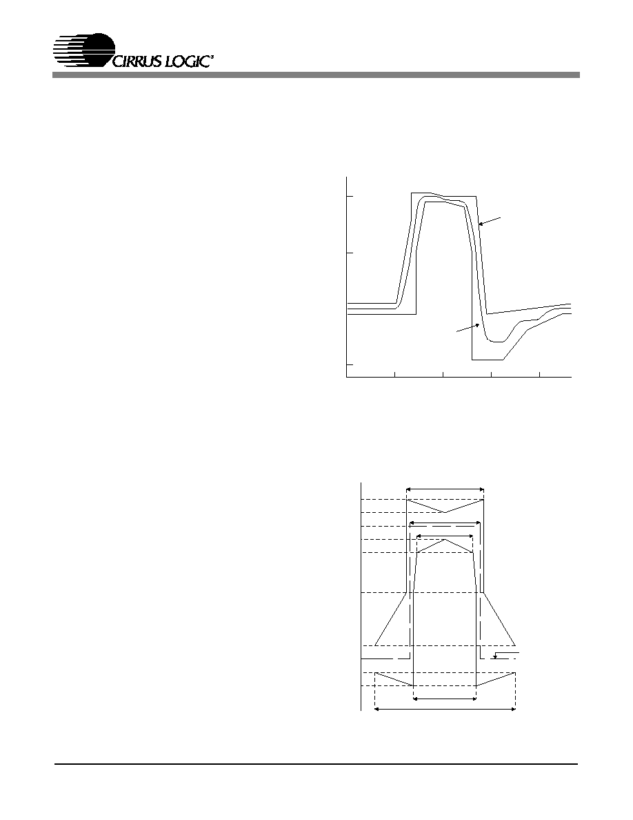
CS61884
24
DS485PP4
9. TRANSMITTER
The CS61884 contains eight identical transmitters
that each use a low power matched impedance driv-
er to eliminate the need for external load matching
resistors, while providing superior return loss. As a
result, the TTIP/TRING outputs can be connected
directly to the transformer allowing one hardware
circuit for 100
(T1/J1), 120 (E1), and 75
(E1) applications.
Digital transmit data is input into the CS61884
through the TPOS/TNEG input pins. These pins ac-
cept data in one of three formats: unipolar, bipolar,
or RZ. In either unipolar or bipolar mode, the
CS61884 internally generates a pulse shape com-
pliant to the ANSI T1.102 mask for T1/J1 or the
G.703 mask for E1 (Refer to
Figure 6
and
Figure 7
). The pulse shaping applied to the transmit
data can be selected in hardware mode or in host
mode.
In hardware mode, the pulse shape is selected for
all channels via the LEN[2:0] pins (Refer to
Table 5 on page 25
). This sets the pulse shape for
all eight transmitters to one of the prestored line
lengths. The CBLSEL pin in combination with the
LEN[2:0] pins set the line impedance for all eight
channels. The CBLSEL pin also selects between
E1 120
or E1 75 modes, when the LEN pins are
configured for E1 operation mode.
In host mode, the pulse shape for each channel can
be set independently, during NRZ operation mode,
for proper clock recovery and jitter attenuation. In
RZ Mode each channel can be set to either T1/J1 or
E1, when there is no Mclk present (Refer to
RZ
Mode
(See Section 9.3 on page 25).
To select the standard pulse shapes, the channels
are selected individually using the
Line Length
Channel ID Register (10h)
(See Section 14.17 on
page 38), then the LEN[3:0] bits in the
Line
Length Data Register (11h)
(See Section 14.18 on
page 39) are set for the desired line length for that
channel. The LEN bits select the line type and im-
pedance for both the receiver and the transmitter of
the addressed channel.
NOTE: In host mode the CBLSEL pin is not used.
5 0 0
1 .0
0 .5
0
-0.5
0
2 5 0
7 50
10 0 0
Normalized
Amplitude
Output Pulse
Shape
ANSI T1.102,
AT&T CB 119
Specifications
TIME (nanoseconds)
Figure 6. Pulse Mask at T1/J1 Interface
Figure 7. Pulse Mask at E1 Interface
000000000000000000000000000000000000
000000000000000000000000000000000000
000000000000000000000000000000000000
000000000000000000000000000000000000
000000000000000000000000000000000000
000000000000000000000000000000000000
000000000000000000000000000000000000
000000000000000000000000000000000000
000000000000000000000000000000000000
000000000000000000000000000000000000
000000000000000000000000000000000000
000000000000000000000000000000000000
000000000000000000000000000000000000
000000000000000000000000000000000000
000000000000000000000000000000000000
000000000000000000000000000000000000
000000000000000000000000000000000000
000000000000000000000000000000000000
000000000000000000000000000000000000
000000000000000000000000000000000000
000000000000000000000000000000000000
000000000000000000000000000000000000
000000000000000000000000000000000000
000000000000000000000000000000000000
000000000000000000000000000000000000
000000000000000000000000000000000000
000000000000000000000000000000000000
000000000000000000000000000000000000
000000000000000000000000000000000000
000000000000000000000000000000000000
000000000000000000000000000000000000
000000000000000000000000000000000000
000000000000000000000000000000000000
000000000000000000000000000000000000
000000000000000000000000000000000000
000000000000000000000000000000000000
000000000000000000000000000000000000
000000000000000000000000000000000000
000000000000000000000000000000000000
000000000000000000000000000000000000
000000000000000000000000000000000000
000000000000000000000000000000000000
000000000000000000000000000000000000
000000000000000000000000000000000000
000000000000000000000000000000000000
000000000000000000000000000000000000
000000000000000000000000000000000000
000000000000000000000000000000000000
000000000000000000000000000000000000
000000000000000000000000000000000000
000000000000000000000000000000000000
000000000000000000000000000000000000
000000000000000000000000000000000000
000000000000000000000000000000000000
000000000000000000000000000000000000
000000000000000000000000000000000000
000000000000000000000000000000000000
000000000000000000000000000000000000
000000000000000000000000000000000000
000000000000000000000000000000000000
000000000000000000000000000000000000
000000000000000000000000000000000000
000000000000000000000000000000000000
000000000000000000000000000000000000
000000000000000000000000000000000000
000000000000000000000000000000000000
000000000000000000000000000000000000
000000000000000000000000000000000000
000000000000000000000000000000000000
000000000000000000000000000000000000
000000000000000000000000000000000000
000000000000000000000000000000000000
000000000000000000000000000000000000
000000000000000000000000000000000000
000000000000000000000000000000000000
000000000000000000000000000000000000
000000000000000000000000000000000000
000000000000000000000000000000000000
2 69 ns
2 44 ns
1 94 ns
2 19 ns
4 88 ns
N om ina l P u ls e
0
10
50
80
90
100
110
120
-10
-20
P erc en t o f
no m in al pe ak
v olta ge

CS61884
DS485PP4
25
The CS61884 also allows the user to customize the
transmit pulse shapes to compensate for non-stan-
dard cables, transformers, or protection circuitry.
For further information on the AWG Refer to
Ar-
bitrary Waveform Generator
(See Section 15 on
page 43).
For more information on the host mode registers,
refer to
Register Descriptions
(See Section 14 on
page 35).
9.1 Bipolar Mode
Bipolar mode provides transparent operation for
applications in which the line coding function is
performed by an external framing device. In this
mode, the falling edge of TCLK samples NRZ data
on TPOS/TNEG for transmission on TTIP/TRING.
9.2 Unipolar Mode
In unipolar mode, the CS61884 is configured such
that transmit data is encoded using B8ZS, HDB3,
or AMI line codes. This mode is activated by hold-
ing TNEG/UBS "High" for more than 16 TCLK
cycles. Transmit data is input to the part via the
TPOS/TDATA pin on the falling edge of TCLK.
When operating the part in hardware mode, the
CODEN pin is used to select between B8ZS/HDB3
or AMI encoding. During host mode operation, the
line coding is selected via the
Global Control Reg-
ister (0Fh)
(See Section 14.16 on page 38).
NOTE: The encoders/decoders are selected for all
eight channels in both hardware and host
mode.
9.3 RZ Mode
In RZ mode, the internal pulse shape circuitry is
bypassed and RZ data driven into TPOS/TNEG is
transmitted on TTIP/TRING. In this mode, the
pulse width of the transmitter output is determined
by the width of the RZ signal input to
TPOS/TNEG. This mode is entered when MCLK
does not exist and TCLK is held "High" for at least
12
µsec.
9.4 Transmitter Powerdown / High-Z
The transmitters can be forced into a high imped-
ance, low power state by holding TCLK of the ap-
propriate channel low for at least 12
µs or 140
MCLK cycles. In hardware and host mode, the
TXOE pin forces all eight transmitters into a high
impedance state within 1
µs.
In host mode, each transmitter is individually con-
trollable using the
Output Disable Register (12h)
(See Section 14.19 on page 39). The TXOE pin can
be used in host mode, but does not effect the con-
tents of the Output Enable Register. This feature is
useful in applications that require redundancy.
9.5 Transmit All Ones (TAOS)
When TAOS is activated, continuous ones are
transmitted on TTIP/TRING using MCLK as the
transmit timing reference. In this mode, the TPOS
and TNEG inputs are ignored.
In hardware mode, TAOS is activated by pulling
TCLK "High" for more than 16 MCLK cycles.
Table 5. Hardware Mode Line Length Configuration Selection
LEN[2:0]
Transmit Pulse Configuration
Line Z
Operation
000
E1 3.0V / E1 2.37V
120
/ 75
E1
001
DS1, Option A (undershoot)
100
T1/J1
010
DS1, Option A (0 dB)
100
T1/J1
011
DSX-1: 0-133 ft. (0.6dB)
100
T1/J1
100
DSX-1: 133-266 ft. (1.2dB)
100
T1/J1
101
DSX-1: 266-399 ft. (1.8dB)
100
T1/J1
110
DSX-1: 399-533 ft. (2.4dB)
100
T1/J1
111
DSX-1: 533-655 ft. (3.0dB)
100
T1/J1

CS61884
26
DS485PP4
In host mode, TAOS is generated for a particular
channel by asserting the associated bit in the
TAOS
Enable Register (03h)
(See Section 14.4 on
page 35).
Since MCLK is the reference clock, it should be of
adequate stability.
9.6 Automatic TAOS
While a given channel is in the LOS condition, if
the corresponding bit in the
Automatic TAOS
Register (0Eh)
(See Section 14.15 on page 37) is
set, the device will drive that channel's TTIP and
TRING with the all ones pattern. This function is
only available in host mode. Refer to
Loss-of-Sig-
nal (LOS)
(See Section 10.5 on page 27).
9.7 Driver Failure Monitor
In host mode, the Driver Failure Monitor (DFM)
function monitors the output of each channel and
sets a bit in the
DFM Status Register (05h)
(See
Section 14.6 on page 35) if a secondary short cir-
cuit is detected between TTIP and TRING. This
generates an interrupt if the respective bit in the
DFM Interrupt Enable Register (07h)
(See Sec-
tion 14.8 on page 36) is also set. Any change in the
DFM Status Register (05h)
(See Section 14.6 on
page 35) will result in the corresponding bit in the
DFM Interrupt Status Register (09h)
(See Sec-
tion 14.10 on page 36) being set. The interrupt is
cleared by reading the
DFM Interrupt Status
Register (09h)
(See Section 14.10 on page 36).
This feature works in all modes of operation E1 75
, E1 120 and T1/J1 100 .
9.8 Driver Short Circuit Protection
The CS61884 provides driver short circuit protec-
tion when current on the secondary exceeds 50 mA
RMS during E1/T1/J1 operation modes.
10. RECEIVER
The CS61884 contains eight identical receivers that
utilize an internal matched impedance technique
that provides for the use of a common set of exter-
nal components for 100
(T1/J1), 120 (E1), and
75
(1) operation (Refer to
Figure 17 on
page 51
). This feature enables the use of a one
stuffing option for all E1/T1/J1 line impedances.
The appropriate E1/T1/J1 line matching is selected
via the LEN[2:0] and the CBLSEL pins in hard-
ware mode, or via the
Line Length Channel ID
Register (10h)
(See Section 14.17 on page 38) and
bits[3:0] of the
Line Length Data Register (11h)
(See Section 14.18 on page 39) in host mode. The
receivers can also be configured to use different ex-
ternal resistors to match the line impedance for E1
75
, E1 120 or T1/J1 100 modes (Refer to
Figure 18 on page 52
).
The CS61884 receiver provides all of the circuitry
to recover both data and clock from the data signal
input on RTIP and RRING. The matched imped-
ance receiver is capable of recovering signals with
12 dB of attenuation (referenced to 2.37 V or 3.0V
nominal) while providing superior return loss. In
addition, the timing recovery circuit along with the
jitter attenuator provide jitter tolerance that far ex-
ceeds jitter specifications (Refer to
Figure 20 on
page 58
).
The recovered data and clock is output from the
CS61884 on RPOS/RNEG and RCLK. These pins
output the data in one of three formats: bipolar, un-
ipolar, or RZ. The CLKE pin is used to configure
RPOS/RNEG, so that data is valid on either the ris-
ing or falling edge of RCLK.
10.1 Bipolar Output Mode
Bipolar mode provides a transparent clock/data re-
covery for applications in which the line decoding
is performed by an external framing device. The re-
covered clock and data are output on RCLK,
RNEG/BPV, and RPOS/RDATA.
10.2 Unipolar Output Mode
In unipolar mode, the CS61884 decodes the recov-
ered data with either B8ZS, HDB3 or AMI line de-
coding. The decoded data is output on the

CS61884
DS485PP4
27
RPOS/RDATA pin. When bipolar violations are
detected by the decoder, the RNEG/BPV pin is as-
serted "High". This pin is driven "high" one RCLK
period for every bipolar violation that is not part of
the zero substitution rules. Unipolar mode is en-
tered by holding the TNEG pin "High" for more
than 16 MCLK cycles.
In hardware mode, the B8ZS/HDB3/AMI encod-
ing/Decoding is activated via the CODEN pin. In
host mode, the
Global Control Register (0Fh)
(See Section 14.16 on page 38) is used to select the
encoding/decoding for all channels.
10.3 RZ Output Mode
In this mode the RTIP and RRING inputs are sliced
to data values that are output on RPOS and RNEG.
This mode is used in applications that have clock
recovery circuitry external to the LIU. To support
external clock recovery, the RPOS and RNEG out-
puts are XORed and output on an edge of RCLK.
This mode is entered when MCLK is tied high.
NOTE: The valid RCLK edge of the RPOS/RNEG data
is controlled by the CLKE pin.
10.4 Receiver Powerdown/High-Z
All eight receivers are powered down when MCLK
is held low. In addition, this will force the RCLK,
RPOS, and RNEG outputs into a high impedance
state.
10.5 Loss-of-Signal (LOS)
The CS61884 makes use of both analog and digital
LOS detection circuitry that is compliant to the lat-
est specifications. During T1/J1 operation ANSI
T1.231 is supported and in E1 operation mode, ei-
ther ITU G.775 or ETSI 300 233 is supported. The
LOS condition in E1 mode is changed from ITU
G.775 to ETSI 300 233 in the
LOS/AIS Mode En-
able Register (0Dh)
(See Section 14.14 on
page 37).
The LOS detector increments a counter each time a
zero is received, and resets the counter each time a
one "mark" is received. Depending on LOS detec-
tion mode, the LOS signal is set when a certain
number of consecutive zeros are received. In
Clock/Data recovery mode, this forces the recov-
ered clock to be replaced by MCLK at the RCLK
output. In addition the RPOS/RNEG outputs are
forced "high" for the length of the LOS period ex-
cept when local and analog loopback are enabled.
Upon exiting LOS, the recovered clock replaces
MCLK on the RCLK output. In Data recovery
mode, RCLK is not replaced by MCLK when LOS
is active. The LOS detection modes are summa-
rized below.
NOTE: T1.231, G.775 and ETSI 300 233 are all avail-
able in host mode, but in hardware mode only
ETSI 300 233 and T1.231 are available.
ANSI T1.231 (T1/J1 Mode Only) - LOS is detect-
ed if the receive signal is less than 200 mV for a pe-
riod of 176 continuous pulse periods. The channel
exits the LOS condition when the pulse density ex-
ceeds 12.5% over 176 pulse periods since the re-
ceipt of the last pulse. An incoming signal with a
pulse amplitude exceeding 250 mV will cause a
pulse transition on the RPOS/RDATA or RNEG
outputs.
ITU G.775 (E1 Mode Only) - LOS is declared
when the received signal level is less than 200 mV
for 32 consecutive pulse periods (typical). The de-
vice exits LOS when the received signal achieves
12.5% ones density with no more than 15 consecu-
tive zeros in a 32 bit sliding window and the signal
level exceeds 250 mV.
ETSI 300 233 (E1 Host Mode Only) - The LOS
indicator becomes active when the receive signal
level drops below 200 mV for more than 2048
pulse periods (1 msec). The channel exits the LOS
state when the input signal exceeds 250 mV and
has transitions for more than 32 pulse periods
(16
µsec). This LOS detection method can only be
selected while in host mode.
CS61884
28
DS485PP4
During host mode operation, LOS is reported in the
LOS Status Monitor Register. Both the LOS pins
and the register bits reflect LOS status in host mode
operation. The LOS pins and status bits are set high
(indicating loss of signal) during reset, power-up,
or channel powered-down.
10.6 Alarm Indication Signal (AIS)
The CS61884 detects all ones alarm condition per
the relevant ANSI, ITU, and ETSI specifications.
In general, AIS is indicated when the one's density
of the receive signal exceeds that dictated by the
relevant specification. This feature is only avail-
able in host mode (Refer to
LOS/AIS Mode En-
able Register (0Dh)
(See Section 14.14 on
page 37)).
ANSI T1.231 AIS (T1/J1 Mode) - The AIS condi-
tion is declared when less than 9 zeros are received
within a sliding window of 8192 bits. This corre-
sponds to a ones density of 99.9% over a period of
5.3 ms. The AIS condition is cleared when nine or
more zeros are detected in a sliding window of
8192 bits.
ITU G.775 AIS (E1 Mode) - The AIS condition is
declared when less than 3 zeros are received within
two consecutive 512 bit windows. The AIS condi-
tion is cleared when 3 or more zeros are received in
two consecutive 512 bit windows.
ETSI 300 233 (E1 Mode) - The AIS condition is
declared when less than 3 zeros are received in a
512 bit window. The AIS condition is cleared when
a 512 bit window is received containing 3 or more
zeros.
11. JITTER ATTENUATOR
The CS61884 internal jitter attenuators can be
switched into either the receive or transmit paths.
Alternatively, it can be removed from both paths to
reduce the propagation delay.
During Hardware mode operation, the location of
the jitter attenuator for all eight channels are con-
trolled by the JASEL pin (Refer to
Table 6
for pin
configurations). The jitter attenuator's FIFO length
and corner frequency, can not be changed in hard-
ware mode. The FIFO length and corner frequency
are set to 32 bits and 1.25Hz for the E1 operational
modes and to 32 bits and 3.78Hz in the T1/J1 oper-
ational modes.
During host mode operation, the location of the jit-
ter attenuator for all eight channels are set by bits 0
and 1 in the
Global Control Register (0Fh)
(See
Section 14.16 on page 38). The GLOBAL CON-
TROL REGISTER (0Fh) also configures the jitter
attenuator's FIFO length (bit 3) and corner fre-
quency (bit 2).
The attenuator consists of a 64-bit FIFO, a narrow-
band monolithic PLL, and control logic. The jitter
attenuator requires no external crystal. Signal jitter
is absorbed in the FIFO which is designed to nei-
ther overflow nor underflow.
If overflow or underflow is imminent, the jitter
transfer function is altered to ensure that no bit-er-
rors occur. A configuration option is provided to
reduce the jitter attenuator FIFO length from 64
bits to 32 bits in order to reduce propagation delay.
The jitter attenuator -3 dB knee frequency depends
on the settings of the Jitter Attenuator FIFO length
and the Jitter Attenuator Corner Frequency bits 2
and 3, in the
Global Control Register (0Fh)
(See
Section 14.16 on page 38)). Setting the lowest cor-
ner frequency guarantees jitter attenuation compli-
ance to European specifications TBR 12/13 and
ETSI ETS 300 011 in E1 mode. The jitter attenua-
tor is also compliant with ITU-T G.735, G.742,
G.783 and AT&T Pub. 62411 (Refer to
Figure 19
on page 58
and
Figure 20 on page 58
).
Table 6. Jitter Attenuator Configurations
PIN STATE
JITTER ATTENUATOR POSITON
LOW
Transmit Path
HIGH
Receive Path
OPEN
Disabled
CS61884
DS485PP4
29
12. OPERATIONAL SUMMARY
A brief summary of the CS61884 operations in hardware and host mode is provided in
Table 7
.
12.1 Loopbacks
The CS61884 provides three loopback modes for
each port. Analog Loopback connects the transmit
signal on TTIP and TRING to RTIP and RRING.
Digital Loopback Connects the output of the En-
coder to the input of the Decoder (through the Jitter
Attenuator if enabled). Remote Loopback connects
the output of the Clock and Data Recovery block to
the input of the Pulse Shaper block. (Refer to de-
tailed descriptions below.) In hardware mode, the
LOOP[7:0] pins are used to activate Analog or Re-
mote loopback for each channel. In host mode, the
Analog, Digital and Remote Loopback registers are
used to enable these functions (Refer to the
Analog
Loopback Register (01h)
(See Section 14.2 on
page 35),
Remote Loopback Register (02h)
(See
Section 14.3 on page 35), and
Digital Loopback
Reset Register (0Ch)
(See Section 14.13 on
page 37).
12.2 Analog Loopback
In
Analog
Loopback,
the
output
of
the
TTIP/TRING driver is internally connected to the
input of the RTIP/RRING receiver so that the data
on TPOS/TNEG and TCLK appears on the
RPOS/RNEG and RCLK outputs. In this mode the
RTIP and RRING inputs are ignored. Refer to
Figure 8 on page 30
. In hardware mode, Analog
Loopback is selected by driving LOOP[7:0] high.
In host mode, Analog Loopback is selected for a
given channel using the appropriate bit in the
Ana-
log Loopback Register (01h)
(See Section 14.2 on
page 35).
NOTE: The simultaneous selection of Analog and
Remote loopback modes is not valid. A TAOS
request overrides the data on TPOS and TNEG
during Analog Loopback. Refer to
Figure 9 on
page 30
.
Table 7. Operational Summary
MCLK
TCLK
LOOP
Receive Mode
Transmit Mode
Loopback
Active
Active
Open
RCLK/Data Recovery
Unipolar/Bipolar
Disabled
Active
Active
L
RCLK/Data Recovery
Unipolar/Bipolar
Remote Loopback
Active
Active
H
RCLK/Data Recovery
Unipolar/Bipolar
Analog Loopback
Active
L
X
RCLK/Data Recovery
Power Down
Disabled
Active
H
Open
RCLK/Data Recovery
TAOS
Disabled
Active
H
L
RCLK/Data Recovery
Unipolar/Bipolar
Remote Loopback
Active
H
H
RCLK/Data Recovery
TAOS
Analog Loopback
L
Active
X
Power Down
Unipolar/Bipolar
Disabled
L
H
X
Power Down
RZ Data
Disabled
L
L
X
Power Down
Power Down
Disabled
H
Active
Open
Data Recovery
Unipolar/Bipolar
Disabled
H
Active
L
Data Recovery
RZ Data
Remote Loopback
H
Active
H
Data Recovery
Unipolar/Bipolar
Analog Loopback
H
L
Open
Data Recovery
Power Down
Disabled
H
L
L
Data Recovery
RZ Data
Remote Loopback
H
L
H
Data Recovery
Power Down
Disabled
H
H
Open
Data Recovery
RZ Data
Disabled
H
H
L
Data Recovery
RZ Data
Remote Loopback
H
H
H
Data Recovery
RZ Data
Analog Loopback

CS61884
30
DS485PP4
12.3 Digital Loopback
Digital Loopback causes the TCLK, TPOS, and
TNEG (or TDATA) inputs to be looped back
through the jitter attenuator (if enabled) to the
RCLK, RPOS, and RNEG (or RDATA) outputs.
The receive line interface is ignored, but data at
TPOS and TNEG (or TDATA) continues to be
transmitted to the line interface at TTIP and
TRING (Refer to
Figure 10 on page 31
).
Digital Loopback is only available during host
mode. It is selected using the appropriate bit in the
Digital Loopback Reset Register (0Ch)
(See Sec-
tion 14.13 on page 37).
NOTE: TAOS can also be used during the Digital Loop-
back operation for the selected channel (Refer
to
Figure 11 on page 31
).
12.4 Remote Loopback
In remote loopback, the RPOS/RNEG and RCLK
outputs are internally input to the transmit circuits
for output on TTIP/TRING. In this mode the
TCLK, TPOS and TNEG inputs are ignored. (Refer
to
Figure 12 on page 31
)
.
In hardware mode, Re-
mote Loopback is selected by driving the LOOP
pin for a certain channel low. In host mode, Remote
Loopback is selected for a given channel by writing
a one to the appropriate bit in the
Remote Loop-
back Register (02h)
(See Section 14.3 on
page 35).
NOTE: In hardware mode, Remote Loopback over-
rides TAOS for the selected channel. In host
mode, TAOS overrides Remote Loopback.
E
n
c
oder
D
e
c
oder
TTIP
TRING
RTIP
RRING
TNEG
TCLK
RNEG
RCLK
TPOS
RPOS
Clock Recovery &
Data Recovery
Transmit
Control &
Pulse Shaper
Ji
tte
r
A
t
t
enuat
or
Ji
tte
r
A
t
t
enuat
or
Figure 8. Analog Loopback Block Diagram
E
n
c
oder
D
e
c
oder
TNEG
TCLK
RNEG
RCLK
TPOS
RPOS
TAOS
MCLK
(All One's)
TTIP
TRING
RTIP
RRING
Clock Recovery &
Data Recovery
Transmit
Control &
Pulse Shaper
Ji
tte
r
A
t
t
enuat
or
Ji
tte
r
A
t
t
enuat
or
Figure 9. Analog Loopback with TAOS Block Diagram

CS61884
DS485PP4
31
E
n
coder
D
e
coder
TNEG
TCLK
RNEG
RCLK
TPOS
RPOS
TTIP
TRING
RTIP
RRING
Clock Recovery &
Data Recovery
Transmit
Control &
Pulse Shaper
Ji
t
t
er
A
t
t
enuat
or
Ji
t
t
er
A
t
t
enuat
or
Figure 10. Digital Loopback Block Diagram
TAOS
MCLK
Encoder
Decoder
TNEG
TCLK
RNEG
RCLK
TPOS
RPOS
TTIP
TRING
RTIP
RRING
Clock Recovery &
Data Recovery
Transmit
Control &
Pulse Shaper
Jitter
Attenuator
Jitter
Attenuator
(All One's)
Figure 11. Digital Loopback with TAOS
E
n
c
oder
Dec
oder
TNEG
TCLK
RNEG
RCLK
TPOS
RPOS
TTIP
TRING
RTIP
RRING
Clock Recovery &
Data Recovery
Transmit
Control &
Pulse Shaper
J
i
tte
r
A
t
t
enuat
or
J
i
tte
r
A
t
t
enuat
or
Figure 12. Remote Loopback Block Diagram

CS61884
32
DS485PP4
13. HOST MODE
Host mode allows the CS61884 to be configured
and monitored using an internal register set. (Refer
to
Table 1, "Operation Mode Selection," on
page 10
). The term, "Host mode" applies to both
Parallel Host and Serial Host modes.
All of the internal registers are available in both Se-
rial and Parallel Host mode; the only difference is
in the functions of the interface pins, which are de-
scribed in
Table 8
.
Serial port operation is compatible with the serial
ports of most microcontrollers. Parallel port opera-
tion can be configured to be compatible with 8-bit
microcontrollers from Motorola or Intel, with both
multiplexed or non-multiplexed address/data bus-
ses. (Refer to
Table 9 on page 34
for host mode
registers).
13.1 SOFTWARE RESET
A software reset can be forced by writing the
Soft-
ware Reset Register (0Ah)
(See Section 14.11 on
page 36). A software reset initializes all registers to
their default settings and initializes all internal state
machines.
13.2 Serial Port Operation
Serial port host mode operation is selected when
the MODE pin is left open or set to VCC/2. In this
mode, the CS61884 register set is accessed by set-
ting the chip select (CS) pin low and communicat-
ing over the SDI, SDO, and SCLK pins. Timing
over the serial port is independent of the transmit
and receive system timing.
Figure 13
illustrates the
format of serial port data transfers.
A read or write is initiated by writing an ad-
dress/command byte (ACB) to SDI. Only the
ADR0-ADR4 bits are valid; bits ADR5-ADR6 are
do not cares. During a read cycle, the register data
addressed by the ACB is output on SDO on the next
eight SCLK clock cycles. During a write cycle, the
data byte immediately follows the ACB.
Data is written to and read from the serial port in
LSB first format. When writing to the port, SDI
data is sampled by the device on the rising edge of
SCLK. The valid clock edge of the data on SDO is
controlled by the CLKE pin. When CLKE is low,
data on SDO is valid on the falling edge of SCLK.
When CLKE is high, data on SDO is valid on the
raising edge of SCLK. The SDO pin is Hi-Z when
not transmitting. If the host processor has a bidirec-
tional I/O port, SDI and SDO may be tied together.
Table 8. Host Control Signal Descriptions
HOST CONTROL SIGNAL DESCRIPTIONS
PIN NAME
PIN #
HARDWARE
SERIAL
PARALLEL
MODE
11
LOW
VDD/2
HIGH
MUX
43
BITSEN0
-
MUX
CODEN/MOT/INTL
88
CODEN
-
MOT/INTL
ADDR [4]
12
GND
-
ADDR[4]
ADDR[3:0]
13-16
ADDR[3:0]
-
ADDR [3:0]
LOOP[7:0], DATA[7:0]
28-21
LOOP[7:0]
-
DATA[7:0]
INT
82
Pulled Up
INT
INT
SDO/ACK/RDY
83
NC
SDO
ACK/RDY
LEN0/SDI/DS/WR
84
LEN0
SDI
DS/WR
LEN1/R/W/RD
85
LEN1
-
R/W/RD
LEN2/SCLK/AS/ALE
86
LEN2
SCLK
AS/ALE
JASEL/CS
87
JASEL
CS
CS

CS61884
DS485PP4
33
As illustrated in
Figure 13
, the ACB consists of a
R/W bit, address field, and two reserved bits. The
R/W bit specifies if the current register access is a
read (R/W = 1) or a write (R/W = 0) operation. The
address field specifies the register address from
0x00 to 0x1f.
13.3 Parallel Port Operation
Parallel port host mode operation is selected when
the MODE pin is high. In this mode, the CS61884
register set is accessed using an 8-bit, multiplexed
bidirectional address/data bus D[7:0]. Timing over
the parallel port is independent of the transmit and
receive system timing.
The device is compatible with both Intel and Mo-
torola bus formats. The Intel bus format is selected
when the MOT/INTL pin is high and the Motorola
bus format is selected when the MOT/INTL pin is
low. In either mode, the interface can have the ad-
dress and data multiplexed over the same 8-bit bus
or on separate busses. This operation is controlled
with the MUX pin; MUX = 1 means that the paral-
lel port has its address and data multiplexed over
the same bus; MUX = 0 defines a non-multiplexed
bus. The timing for the different modes are shown
in
Figure 26
,
Figure 27
,
Figure 28
,
Figure 29
,
Figure 30
,
Figure 31
,
Figure 32
and
Figure 33
.
Non-multiplexed Intel and Motorola modes are
shown in
Figure 30
,
Figure 31
,
Figure 32
and
Figure 33
. The CS pin initiates the cycle, followed
by the DS, RD or WR pin. Data is latched into or
out of the part using the rising edge of the DS, WR
or RD pin. Raising CS ends the cycle.
Multiplexed Intel and Motorola modes are shown
in
Figure 26
,
Figure 27
,
Figure 28
and
Figure 29
. A
read or write is initiated by writing an address byte
to D[7:0]. The device latches the address on the
falling edge of ALE(AS). During a read cycle, the
register data is output during the later portion of the
RD or DS pulses. The read cycle is terminated and
the bus returns to a high impedance state as RD
transitions high in Intel timing or DS transitions
high in Motorola timing. During a write cycle, val-
id write data must be present and held stable during
the WR or DS pulses.
In Intel mode, the RDY output pin is normally in a
high impedance state; it pulses low once to ac-
knowledge that the chip has been selected, and high
again to acknowledge that data has been written or
read. In Motorola mode, the ACK pin performs a
similar function; it drives high to indicate that the
address has been received by the part, and goes low
again to indicate that data has been written or read.
CS
SDI
SCLK
SDO
CLKE=0
0
R/W
0
0
0
0
0
1
D0
D1
D2
D5
D3
D6
D4
D7
D0
D1
D2
D5
D3
D6
D4
D7
Address/Command Byte
Data Input/Output
Figure 13. Serial Read/Write Format (SPOL = 0)

CS61884
34
DS485PP4
13.4 Register Set
The register set available during host mode opera-
tions are presented in
Table 9
. While the upper
three bits of the parallel address are don't cares on
the CS61884, they should be set to zero for proper
operation.
Table 9. Host Mode Register Set
REGISTERS
BITS
ADDR
NAME
TYPE
7
6
5
4
3
2
1
0
00h
Revision/IDCODE
R
IDCODE Refer to
Device ID Register (IDR)
on page 48
01h
Analog Loopback
R/W
ALBK 7
ALBK 6
ALBK 5
ALBK 4
ALBK 3
ALBK 2
ALBK 1
ALBK 0
02h
Remote Loopback
R/W
RLBK 7
RLBK 6
RLBK 5
RLBK 4
RLBK 3 RLBK 2
RLBK 1
RLBK 0
03h
TAOS Enable
R/W
TAOE 7
TAOE 6
TAOE 5
TAOE 4
TAOE 3
TAOE 2 TAOE 1
TAOE 0
04h
LOS Status
R
LOSS 7
LOSS 6
LOSS 5
LOSS 4
LOSS 3 LOSS 2 LOSS 1
LOSS 0
05h
DFM Status
R
DFMS 7 DFMS 6 DFMS 5 DFMS 4 DFMS 3 DFMS 2 DFMS 1 DFMS 0
06h
LOS Interrupt Enable
R/W
LOSE 7
LOSE 6
LOSE 5
LOSE 4
LOSE 3 LOSE 2 LOSE 1
LOSE 0
07h
DFM Interrupt Enable
R/W
DFME 7 DFME 6 DFME 5 DFME 4 DFME 3 DFME 2 DFME 1 DFME 0
08h
LOS Interrupt Status
R
LOSI 7
LOSI 6
LOSI 5
LOSI 4
LOSI 3
LOSI 2
LOSI 1
LOSI 0
09h
DFM Interrupt Status
R
DFMI 7
DFMI 6
DFMI 5
DFMI 4
DFMI 3
DFMI 2
DFMI 1
DFMI 0
0Ah
Software Reset
R/W
SRES 7 SRES 6 SRES 5 SRES 4 SRES 3 SRES 2 SRES 1 SRES 0
0Bh
Performance Monitor
R/W
RSVD
RSVD
RSVD
RSVD
A3
A2
A1
A0
0Ch
Digital Loopback
R/W
DLBK 7
DLBK 6
DLBK 5
DLBK 4
DLBK 3 DLBK 2
DLBK 1
DLBK 0
0Dh
LOS/AIS Mode Enable
R/W
LAME 7 LAME 6 LAME 5 LAME 4 LAME 3 LAME 2 LAME 1 LAME 0
0Eh
Automatic TAOS
R/W
ATAO 7
ATAO 6
ATAO 5
ATAO 4
ATAO 3
ATAO 2
ATAO 1
ATAO 0
0Fh
Global Control
R/W
AI
Raisen
RSVD
Coden
FIFO
JACF
JASEL [1:0]
10h
Line Length Channel ID
R/W
RSVD
RSVD
RSVD
RSVD
RSVD
Channel ID
11h
Line Length Data
R/W
RSVD
RSVD
RSVD
IN_EX
LEN[3:0]
12h
Output Disable
R/W
OENB 7 OENB 6 OENB 5 OENB 4 OENB 3 OENB 2 OENB 1 OENB 0
13h
AIS Status
R
AISS 7
AISS 6
AISS 5
AISS 4
AISS 3
AISS 2
AISS 1
AISS 0
14h
AIS Interrupt Enable
R/W
AISE 7
AISE 6
AISE 5
AISE 4
AISE 3
AISE 2
AISE 1
AISE 0
15h
AIS Interrupt Status
R
AISI 7
AISI 6
AISI 5
AISI 4
AISI 3
AISI 2
AISI 1
AISI 0
16h
AWG Broadcast
R/W AWGB 7 AWGB 6 AWGB 5 AWGB 4 AWGB 3 AWGB 2 AWGB 1 AWGB 0
17h
AWG Phase Address
R/W
Channel Address [2:0]
Phase Address [4:0]
18h
AWG Phase Data
R/W
RSVD
Sample Data[6:0]
19h
AWG Enable
R/W AWGN 7 AWGN 6 AWGN 5 AWGN 4 AWGN 3 AWGN 2 AWGN 1 AWGN 0
1Ah
AWG Overflow Interrupt Enable R/W AWGE 7 AWGE 6 AWGE 5 AWGE 4 AWGE 3 AWGE 2 AWGE 1 AWGE 0
1Bh
AWG Overflow Interrupt Status
R
AWGI 7
AWGI 6
AWGI 5
AWGI 4
AWGI 3
AWGI 2 AWGI 1
AWGI 0
1Ch
RESERVED
R/W
RSVD 6 RSVD 5 RSVD 4 RSVD 3 RSVD 2 RSVD 1 RSVD 0 RSVD 6
1Dh
RESERVED
R
RSVD 6 RSVD 5 RSVD 4 RSVD 3 RSVD 2 RSVD 1 RSVD 0 RSVD 6
1Eh
BITS Clock Enable
R/W
BITS 7
BITS 6
BITS 5
BITS 4
BITS 3
BITS 2
BITS 1
BITS 0
1Fh
RESERVED
R/W
RSVD 7 RSVD 6 RSVD 5 RSVD 4 RSVD 3 RSVD 2 RSVD 1 RSVD 0

CS61884
DS485PP4
35
14. REGISTER DESCRIPTIONS
14.1 Revision/IDcode Register (00h)
14.2
Analog Loopback Register (01h)
14.3 Remote Loopback Register (02h)
14.4
TAOS Enable Register (03h)
14.5 LOS Status Register (04h)
14.6
DFM Status Register (05h)
BIT
NAME
Description
[7:4]
REVI 7-4
Bits [7:4] are taken from the least-significant nibble of the Device IDCode, which are 0100.
(Refer to
Device ID Register (IDR)
(See Section 16.3 on page 48).
[3:0]
REVI 3-0
Bits [3:0] are the revision bits from the JTAG IDCODE register, CS61884 Revision A = 0000.
These bits are subject to change with the revision of the device (Refer to
Device ID Register
(IDR)
(See Section 16.3 on page 48).
BIT
NAME
Description
[7:0]
ALBK 7-0
Enables analog loopbacks. A "1" in bit n enables the loopback for channel n. Refer to
Analog
Loopback
(See Section 12.2 on page 29) for a complete explanation. Register bits default
to 00h after power-up or reset.
BIT
NAME
Description
[7:0]
RLBK 7-0
Enables remote loopbacks. A "1" in bit n enables the loopback for channel n. Refer to
Remote Loopback
(See Section 12.4 on page 30) for a complete explanation. Register bits
default to 00h after power-up or reset.
BIT
NAME
Description
[7:0]
TAOE 7-0
A "1" in bit n of this register turns on the TAOS generator in channel n. Register bits default
to 00h after power-up or reset.
BIT
NAME
Description
[7:0]
LOSS 7-0
Register bit n is read as "1" when LOS is detected on channel n. Register bits default to
00h after power-up or reset.
BIT
NAME
Description
[7:0]
DFMS 7-0 Driver Failure Monitor. The DFM will set bit n to "1" when it detects a short circuit in channel
n. Register bits default to 00h after power-up or reset.

CS61884
36
DS485PP4
14.7 LOS Interrupt Enable Register (06h)
14.8 DFM Interrupt Enable Register (07h)
14.9
LOS Interrupt Status Register (08h)
14.10
DFM Interrupt Status Register (09h)
14.11 Software Reset Register (0Ah)
14.12 Performance Monitor Register (0Bh)
BIT
NAME
Description
[7:0]
LOSE 7-0
Any change in a LOS Status Register bits will cause the INT pin to go low if corresponding bit
in this register is set to "1". Register bits default to 00h after power-up or reset.
BIT
NAME
Description
[7:0]
DFME 7-0
Enables interrupts for failures detected by the DFM. Any change in a DFM Status Register bit
will cause an interrupt if the corresponding bit is set to "1" in this register. Register bits
default to 00h after power-up or reset.
BIT
NAME
Description
[7:0]
LOSI 7-0
Bit n of this register is set to "1" to indicate a status change in bit n of the LOS Status Regis-
ter. The bits in this register indicate a change in status since the last cleared LOS interrupt.
Register bits default to 00h after power-up or reset.
BIT
NAME
Description
[7:0]
DFMI 7-0
Bit n of this register is set to "1" to indicate a status change in bit n of the DFM Status Regis-
ter. The bits in this register indicate a change in status since the last cleared DFM interrupt.
Register bits default to 00h after power-up or reset.
BIT
NAME
Description
[7:0]
SRES 7-0 Writing to this register initializes all registers to their default settings. Register bits default to
00h after power-up or reset.
BIT
NAME
Description
[7:4]
RSVD 7-4
RESERVED (These bits must be set to 0.)

CS61884
DS485PP4
37
14.13 Digital Loopback Reset Register (0Ch)
14.14 LOS/AIS Mode Enable Register (0Dh)
14.15 Automatic TAOS Register (0Eh)
[3:0]
A[3:0]
The G.772 Monitor is directed to a given channel based on the state of the four least signifi-
cant bits of this register. Register bits default to 00h after power-up or reset. The follow-
ing table shows the settings needed to select a specific channel's receiver or transmitter to
perform G.772 monitoring.
A[3:0]
Channel Selection
0000
Monitoring Disabled
0001
RX Channel #1
0010
RX Channel #2
0011
RX Channel #3
0100
RX Channel #4
0101
RX Channel #5
0110
RX Channel #6
0111
RX Channel #7
1000
Monitoring Disabled
1001
TX Channel #1
1010
TX Channel #2
1011
TX Channel #3
1100
TX Channel #4
1101
TX Channel #5
1110
TX Channel #6
1111
TX Channel #7
BIT
NAME
Description
[7:0]
DLBK 7-0
Setting register bit n to "1" enables the digital loopback for channel n. Refer to
Digital Loop-
back
(See Section 12.3 on page 30) for a complete explanation. Register bits default to
00h after power-up or reset.
BIT
NAME
Description
[7:0]
LAME 7-0 T1/J1 MODE - These bits are "Do Not Care", T1.231 Compliant LOS/AIS already used.
E1 Mode - Setting bit n to "1" enables ETSI 300 233 compliant LOS/AIS for channel n; set-
ting bit n to "0" enables ITU G.775 compliant LOS/AIS for channel n. Register bits default to
00h after power-up or reset.
BIT
NAME
Description
[7:0]
ATAO 7-0
Setting bit n to "1" enables automatic TAOS generation on channel n when LOS is detected.
Register bits default to 00h after power-up or reset.
(Continued)
BIT
NAME
Description
CS61884
38
DS485PP4
14.16 Global Control Register (0Fh)
14.17 Line Length Channel ID Register (10h)
BIT
NAME
Description
This register is the global control for the AWG Auto-Increment, Automatic AIS insertion,
encoding/decoding and the jitter attenuators location, FIFO length and corner frequency for
all eight channels. Register bits default to 00h after power-up or reset.
[7]
AWG Auto-
Increment
The AWG Auto-Increment bit indicates whether to auto-increment the
AWG Phase Address
Register (17h)
(See Section 14.24 on page 40) after each access. Thus, when this bit is set,
the phase samples address portion of the address register increments after each read or
write access. This bit must be set before any bit in the AWG Enable register is set, if this
function is required.
[6]
RAISEN
On LOS, this bit controls the automatic AIS insertion into all eight receiver paths.
0 = Disabled
1 = Enabled
[5]
RSVD
RESERVED (This bit must be set to 0.)
[4]
CODEN
Line encoding/decoding Selection
0 = B8ZS/HDB3 (T1/J1/E1 respectively)
1 = AMI
[3]
FIFO
LENGTH
Jitter Attenuator FIFO length Selection
0 = 32 bits
1 = 64 bits
[2]
JACF
Jitter Attenuator Corner Frequency Selection
E1
T1/J1
0 = 1.25Hz
3.78Hz
1 = 2.50Hz
7.56Hz
[1:0]
JASEL [1:0]
These bits select the position of the Jitter Attenuator.
BIT
NAME
Description
[7:3]
RSVD 7-3
RESERVED (These bits must be set to 0.)
[2:0]
LLID 2-0
The value written to these bits specify the LIU channel for which the Pulse Shape Configura-
tion Data (register 11h) applies. For example, writing a value of a binary 000 to the 3-LSBs
will select channel 0. The pulse shape configuration data for the channel specified in this reg-
ister are written or read through the Line Length Data Register (11h). Register bits default
to 00h after power-up or reset.
JASEL 1 JASEL 0
POSITION
0
0
Disabled
0
1
Transmit Path
1
0
Disabled
1
1
Receive Path

CS61884
DS485PP4
39
14.18 Line Length Data Register (11h)
14.19 Output Disable Register (12h)
14.20 AIS Status Register (13h)
14.21 AIS Interrupt Enable Register (14h)
BIT
NAME
Description
The value written to the 4-LSBs of this register specifies whether the device is operating in
either T1/J1 or E1 modes and the associated pulse shape as shown below is being transmit-
ted. Register bits default to 00h after power-up or reset.
[7:5]
RSVD
RESERVED (These bits must be set to 0.)
[4]
INT_EXTB
This bit specifies the use of internal (Int_ExtB = 1) or external (Int_ExtB = 0) receiver line
matching. The line impedance for both the receiver and transmitter are chosen through the
LEN [3:0] bits in this register.
[3:0]
LEN[3:0]
These bits setup the line impedance for both the receiver and the transmitter path and the
desired pulse shape for a specific channel. The channel is selected with the Line Length
Channel ID register (0x10). The following table shows the available transmitter pulse
shapes.
LEN [3:0]
Operation
Mode
Line Length Selection
Phase Samples
per UI
0000
E1
120
3.0V
12
0001
T1/J1
100
DS1, Option A (undershoot)
14
0010
T1/J1
100
DS1, Option A (0dB)
14
0011
T1/J1
100
0 - 133Ft (0.6dB)
13
0100
T1/J1
100
133 - 266Ft (1.2dB)
13
0101
T1/J1
100
266 - 399Ft (1.2dB)
13
0110
T1/J1
100
399 - 533Ft (2.4dB)
13
0111
T1/J1
100
533 - 655Ft (3.0dB)
13
1000
E1
75
2.37V
12
BIT
NAME
Description
[7:0]
OENB 7-0 Setting bit n of this register to "1" High-Z the TX output driver on channel n of the device.
Register bits default to 00h after power-up or reset.
BIT
NAME
Description
[7:0]
AISS 7-0
A "1" in bit position n indicates that the receiver has detected an AIS condition on channel n,
which generates an interrupt on the INT pin. Register bits default to 00h after power-up or
reset.
BIT
NAME
Description
[7:0]
AISE 7-0
This register enables changes in the AIS Status register to be reflected in the AIS Interrupt
Status register, thus causing an interrupt on the INT pin. Register bits default to 00h after
power-up or reset.

CS61884
40
DS485PP4
14.22 AIS Interrupt Status Register (15h)
14.23 AWG Broadcast Register (16h)
14.24 AWG Phase Address Register (17h)
14.25 AWG Phase Data Register (18h)
14.26 AWG Enable Register (19h)
BIT
NAME
Description
[7:0]
AISI 7-0
Bit n is set to "1" to indicate a change of status of bit n in the AIS Status Register. The bits in
this register indicate which channel changed in status since the last cleared AIS interrupt.
Register bits default to 00h after power-up or reset.
BIT
NAME
Description
[7:0]
AWGB 7-0
Setting bit n to "1" causes the phase data in the AWG Phase Data Register to be written to
the corresponding channel or channels simultaneously. (Refer to
Arbitrary Waveform Gen-
erator
(See Section 15 on page 43). Register bits default to 00h after power-up or reset.
BIT
NAME
Description
[7:5]
AWGA
These bits specify the target channel 0-7. (Refer to
Arbitrary Waveform Generator
(See
Section 15 on page 43). Register bits default to 00h after power-up or reset.
[4:0]
PA[4:0]
These bits specify 1 of 24 (E1) or 26/28 (T1/J1) phase sample address locations of the AWG,
that the phase data in the AWG Phase Data Register is written to or read from. The other
locations in each channel's phase sample addresses are not used, and should not be
accessed. Register bits default to 00h after power-up or reset.
BIT
NAME
Description
[7]
RSVD
RESERVED (This bit must be set to 0.)
[6:0]
AWGD [6:0]
These bits are used for the pulse shape data that will be written to the AWG phase location
specified by the AWG Phase Address Register. The value written to or read from this register
will be written to or read from the AWG phase sample location specified by the AWG Phase
Address register. A software reset through the Software Reset Register does not effect the
contents of this register. The data in each phase is a 7-bit 2's complement number (the max-
imum positive value is 3Fh and the maximum negative value is 40h). (Refer to
Arbitrary
Waveform Generator
(See Section 15 on page 43). Register bits default to 00h after
power-up.
BIT
NAME
Description
[7:0]
AWGN 7-0
The AWG enable register is used for selecting the source of the customized transmission
pulse-shape. Setting bit n to "1" in this register selects the AWG as the source of the output
pulse shape for channel n. When bit n is set to "0" the pre-programmed pulse shape in the
ROM is selected for transmission on channel n. (Refer to
Arbitrary Waveform Generator
(See Section 15 on page 43). Register bits default to 00h after power-up or reset.

CS61884
DS485PP4
41
14.27
AWG Overflow Interrupt Enable Register (1Ah)
14.28 AWG Overflow Interrupt Status Register (1Bh)
14.29 Reserved Register (1Ch)
14.30 Reserved Register (1Dh)
14.31 Bits Clock Enable Register (1Eh)
14.32 Reserved Register (1Fh)
BIT
NAME
Description
[7:0]
AWGE 7-0
This register enables changes in the overflow status to be reflected in the AWG Interrupt Sta-
tus register, thus causing as interrupt on the INT pin. Interrupts are maskable on a per-chan-
nel basis. Register bits default to 00h after power-up or reset.
BIT
NAME
Description
[7:0]
AWGI 7-0
The bits in this register indicate a change in status since the last AWG overflow interrupt. An
AWG overflow occurs when invalid phase data are entered, such that a sample-by-sample
addition of UI0 and UI1 results in values that exceed the arithmetic range of the 7-bit repre-
sentation. Reading this register clears the interrupt, which deactivates the INT pin. Register
bits default to 00h after power-up or reset.
BIT
NAME
Description
[7:0]
RSVD 7-0
RESERVED (These bits must be set to zero.)
BIT
NAME
Description
[7:0]
RSVD 7-0
RESERVED (These bits must be set to zero.)
BIT
NAME
Description
[7:0]
BITS 7-0
Setting a "1" to bit n in this register changes channel n to a stand-alone timing recovery unit
used for G.703 clock recovery. (Refer to
BUILDING INTEGRATED TIMING SYSTEMS
(BITS) CLOCK MODE
(See Section 8 on page 23) for a better description of the G.703 clock
recovery function). Register bits default to 00h after power-up or reset.
BIT
NAME
Description
[7:0]
RSVD 7-0
RESERVED (These bits must be set to zero.)

CS61884
42
DS485PP4
14.33 Status Registers
The following Status registers are read-only:
LOS
Status Register (04h)
(See Section 14.5 on
page 35),
DFM Status Register (05h)
(See Sec-
tion 14.6 on page 35) and
AIS Status Register
(13h)
(See Section 14.20 on page 39). The
CS61884 generates an interrupt on the INT pin any
time an unmasked status register bit changes.
14.33.1 Interrupt Enable Registers
The Interrupt Enable registers:
LOS Interrupt En-
able Register (06h)
(See Section 14.7 on page 36),
DFM Interrupt Enable Register (07h)
(See Sec-
tion 14.8 on page 36),
AIS Interrupt Enable Reg-
ister (14h)
(See Section 14.21 on page 39) and
AWG Overflow Interrupt Enable Register
(1Ah)
(See Section 14.27 on page 41)
,
enable
changes in status register state to cause an interrupt
on the INT pin. Interrupts are maskable on a per
channel basis. When an Interrupt Enable register
bit is 0, the corresponding Status register bit is dis-
abled from causing an interrupt on the INT pin.
NOTE: Disabling an interrupt has no effect on the sta-
tus reflected in the associated status register.
14.33.2 Interrupt Status Registers
The following interrupt status registers:
LOS In-
terrupt Status Register (08h)
(See Section 14.9
on page 36),
DFM Interrupt Status Register
(09h)
(See Section 14.10 on page 36),
AIS Inter-
rupt Status Register (15h)
(See Section 14.22 on
page 40) and
AWG Overflow Interrupt Status
Register (1Bh)
(See Section 14.28 on page 41), in-
dicate a change in status of the corresponding status
registers in host mode. Reading these registers
clears the interrupt, which deactivates the INT pin.

CS61884
DS485PP4
43
15. ARBITRARY WAVEFORM
GENERATOR
Using the Arbitrary Waveform Generator (AWG)
allows the user to customize the transmit pulse
shapes to compensate for nonstandard cables,
transformers, protection circuitry, or to reduce
power consumption by reducing the output pulse
amplitude. A channel is configured for a custom
pulse shape by storing data representing the pulse
shape into the 24/26/28 phase sample locations and
then enabling the AWG for that channel. Each
channel has a separate AWG, so all eight channels
can have a different customized pulse shape. The
microprocessor interface, is used to read from or
write to the AWG, while the device is in host mode.
In the AWG RAM, the pulse shape is divided into
two unit intervals (UI). For E1 mode, there are 12
sample phases in each UI, while in T1/J1 mode, the
number of sample phases per UI are either 13 or 14.
The first UI is for the main part of the pulse and the
second UI is for the "tail" of the pulse (Refer to
Figure 14
). A complete pulse-shape is represented
by 24 phase samples in E1 mode or 26/28 phase
samples in T1/J1 mode. In E1 mode, data written in
the first UI represents a valid pulse shape, while
data in the second UI is ignored and should be set
to zero.
The mode of operation is selected using the
Line
Length Channel ID Register (10h)
(See Section
14.17 on page 38) and the
Line Length Data Reg-
ister (11h)
(See Section 14.18 on page 39). A
phase sample, or cell, is accessed by first loading
the channel address and the phase sample address
into the
AWG Phase Address Register (17h)
(See
Section 14.24 on page 40), and then reading or
writing the
AWG Phase Data Register (18h)
(See
Section 14.25 on page 40). The upper locations in
each channel's address space are not used; reading
and writing to these registers produces undefined
results.
The data in each phase sample is a 7-bit two's com-
plement number with a maximum positive value of
0x3f, and a maximum negative value of 0x40. The
terms "positive" and "negative" are defined for a
positive going pulse only. The pulse generation cir-
cuitry automatically inverts the pulse for negative
going pulses. The data stored in the lowest phase
address corresponds to the first phase sample that
will be transmitted in time. When the mode of op-
eration calls for only 24/26 phase samples if the
phase samples that are not used (25 through 28) are
written to, they are ignored and don't effect the
shape of the customized pulse shape.
The following procedure describes how to enable
and write data into the AWG to produce custom-
ized pulse shapes to be transmitted for a specific
E1 AWG Example
DSX-1 (54% duty cycle) AWG Example
DSX-1 (50% duty cycle) AWG Example
U1
U2
U1
U2
U1
U2
Figure 14. Arbitrary Waveform UI

CS61884
44
DS485PP4
channel or channels. To enable the AWG function
for a specific channel or channels the correspond-
ing bit(s) in the
AWG Enable Register (19h)
(See
Section 14.26 on page 40) must be set to "1". When
the corresponding bit(s) in the AWG Enable Regis-
ter are set to "0" pre-programmed pulse shapes are
selected for transmission.
In order to access and write data for a customized
pulse shape to a specific channel or channels, the
following steps are required. First the desired chan-
nel and phase sample addresses must be written to
the
AWG Phase Data Register (18h)
(See Section
14.25 on page 40). Once the channel and phase
sample address have been selected, the actual phase
sample data may be entered into the AWG Phase
Data Register at the selected phase sample address
selected by the lower five bits of the
AWG Phase
Address Register (17h)
(See Section 14.24 on
page 40)).
To change the phase sample address of the selected
channel the user may use either of the following
steps. First, the user can re-write the phase sample
address to the AWG Phase Address Register or set
the Auto-Increment bit (Bit 7) in the
Global Con-
trol Register (0Fh)
(See Section 14.16 on
page 38)) to "1". When this bit is set to "1" only the
first phase sample address (00000 binary) needs to
be written to the
AWG Phase Address Register
(17h)
(See Section 14.24 on page 40), and each
subsequent access (read or write) to the
AWG
Phase Data Register (18h)
(See Section 14.25 on
page 40) will automatically increment the phase
sample address. The channel address, however, re-
mains unaffected by the Auto-Increment mode.
Since the number of phase samples forming the
customized pulse shape varies with the mode of op-
eration (E1/T1/J1), the
AWG Phase Address Reg-
ister (17h)
(See Section 14.24 on page 40) needs to
be re-written in order to re-start the phase sample
address sequence from zero.
The AWG Broadcast function allows the same data
to be written to different channels simultaneously.
This is done with the use of the
AWG Broadcast
Register (16h)
(See Section 14.23 on page 40)),
each bit in the AWG Broadcast Register corre-
sponds to a different channel (bit 0 is channel 0, and
bit 3 is channel 3 & etc.).
To write the same pulse shaping data to multiple
channels, simple set the corresponding bit to "1" in
the
AWG Broadcast Register (16h)
(See Section
14.23 on page 40). This function only requires that
one of the eight channel addresses be written to the
AWG Phase Address Register (17h)
(See Section
14.24 on page 40). During an AWG read sequence,
the bits in the AWG Broadcast Register are ig-
nored. During an AWG write sequence, the select-
ed channel or channels are specified by both the
channel address specified by the upper bits of the
AWG Phase Address Register (17h)
(See Section
14.24 on page 40) and the selected channel or chan-
nels in the
AWG Broadcast Register (16h)
(See
Section 14.23 on page 40).
During a multiple channel write the first channel
that is written to, is the channel that was address by
the AWG Phase Address Register. This channel's
bit in the AWG Broadcast Register can be set to ei-
ther "1" or "0". For a more descriptive explanation
of how to use the AWG refer to the "How To Use
The CS61880/CS61884 Arbitrary Waveform Gen-
erator" application note AN204.

CS61884
DS485PP4
45
16. JTAG SUPPORT
The CS61884 supports the IEEE Boundary Scan
Specification as described in the IEEE 1149.1 stan-
dards. A Test Access Port (TAP) is provided that
consists of the TAP controller, the instruction reg-
ister (IR), by-pass register (BPR), device ID regis-
ter (IDR), the boundary scan register (BSR), and
the 5 standard pins (TRST, TCK, TMS, TDI, and
TDO). A block diagram of the test access port is
shown in
Figure 15
. The test clock input (TCK) is
used to sample input data on TDI, and shift output
data through TDO. The TMS input is used to step
the TAP controller through its various states.
The instruction register is used to select test execu-
tion or register access. The by-pass register pro-
vides a direct connection between the TDI input
and the TDO output. The device identification reg-
ister contains an 32-bit device identifier.
The Boundary Scan Register is used to support test-
ing of IC inter-connectivity. Using the Boundary
Scan Register, the digital input pins can be sampled
and shifted out on TDO. In addition, this register
can also be used to drive digital output pins to a
user defined state.
16.1 TAP Controller
The TAP Controller is a 16 state synchronous state
machine clocked by the rising edge of TCK. The
TMS input governs state transitions as shown in
Figure 16
. The value shown next to each state tran-
sition in the diagram is the value that must be on
TMS when it is sampled by the rising edge of TCK.
16.1.1 JTAG Reset
TRST resets all JTAG circuitry.
16.1.2 Test-Logic-Reset
The test-logic-reset state is used to disable the test
logic when the part is in normal mode of operation.
This state is entered by asynchronously asserting
TRST or forcing TMS High for 5 TCK periods.
16.1.3 Run-Test-Idle
The run-test-idle state is used to run tests.
parallel latched
output
Boundary Scan Data Register
Device ID Data Register
Bypass Data Register
Instruction (shift) Register
TAP
Controller
parallel latched output
TDI
TCK
Digital output pins
Digital input pins
JTAG BLOCK
MUX
TDO
TMS
Figure 15. Test Access Port Architecture

CS61884
46
DS485PP4
16.1.4 Select-DR-Scan
This is a temporary controller state.
16.1.5 Capture-DR
In this state, the Boundary Scan Register captures
input pin data if the current instruction is EXTEST
or SAMPLE/PRELOAD.
16.1.6 Shift-DR
In this controller state, the active test data register
connected between TDI and TDO, as determined
by the current instruction, shifts data out on TDO
on each rising edge of TCK.
16.1.7 Exit1-DR
This is a temporary state. The test data register se-
lected by the current instruction retains its previous
value.
16.1.8 Pause-DR
The pause state allows the test controller to tempo-
rarily halt the shifting of data through the current
test data register.
16.1.9 Exit2-DR
This is a temporary state. The test data register se-
lected by the current instruction retains its previous
value.
16.1.10 Update-DR
The Boundary Scan Register is provided with a
latched parallel output to prevent changes while
data is shifted in response to the EXTEST and
SAMPLE/PRELOAD instructions. When the TAP
controller is in this state and the Boundary Scan
Register is selected, data is latched into the parallel
output of this register from the shift-register path
on the falling edge of TCK. The data held at the
latched parallel output changes only in this state.
1
0
Test-Logic-Reset
Run-Test/Idle
Select-DR-Scan
Capture-DR
Shift-DR
Exit1-DR
Pause-DR
Exit2-DR
Update-DR
Select- IR-Scan
Capture- IR
Shift- IR
Exit1- IR
Pause- IR
Exit2- IR
Update- I R
0
1
1
1
1
1
1
1
1
1
1
1
1
1
1
0
0
0
0
0
0
0
0
0
0
0
0
0
1
0
Figure 16. TAP Controller State Diagram

CS61884
DS485PP4
47
16.1.11 Select-IR-Scan
This is a temporary controller state. The test data
register selected by the current instruction retains
its previous state.
16.1.12 Capture-IR
In this controller state, the instruction register is
loaded with a fixed value of "01" on the rising edge
of TCK. This supports fault-isolation of the board-
level serial test data path.
16.1.13 Shift-IR
In this state, the shift register contained in the in-
struction register is connected between TDI and
TDO and shifts data one stage towards its serial
output on each rising edge of TCK.
16.1.14 Exit1-IR
This is a temporary state. The test data register se-
lected by the current instruction retains its previous
value.
16.1.15 Pause-IR
The pause state allows the test controller to tempo-
rarily halt the shifting of data through the instruc-
tion register.
16.1.16 Exit2-IR
This is a temporary state. The test data register se-
lected by the current instruction retains its previous
value.
16.1.17 Update-IR
The instruction shifted into the instruction register
is latched into the parallel output from the shift-reg-
ister path on the falling edge of TCK. When the
new instruction has been latched, it becomes the
current instruction. The test data registers selected
by the current instruction retain their previous val-
ue.
16.2 Instruction Register (IR)
The 3-bit Instruction register selects the test to be
performed and/or the data register to be accessed.
The valid instructions are shifted in LSB first and
are listed in
Table 10
:
16.2.1 EXTEST
The EXTEST instruction allows testing of off-chip
circuitry and board-level interconnect. EXTEST
connects the BSR to the TDI and TDO pins.
16.2.2 SAMPLE/PRELOAD
The SAMPLE/PRELOAD instruction samples all
device inputs and outputs. This instruction places
the BSR between the TDI and TDO pins. The BSR
is loaded with samples of the I/O pins by the Cap-
ture-DR state.
16.2.3 IDCODE
The IDCODE instruction connects the device iden-
tification register to the TDO pin. The device iden-
tification code can then be shifted out TDO using
the Shift-DR state.
16.2.4 BYPASS
The BYPASS instruction connects a one TCK de-
lay register between TDI and TDO. The instruction
is used to bypass the device.
Table 10. JTAG Instructions
IR CODE
INSTRUCTION
000
EXTEST
100
SAMPLE/PRELOAD
110
IDCODE
111
BYPASS

CS61884
48
DS485PP4
16.3 Device ID Register (IDR)
Revision section: 0h = Rev A, 1h = Rev B and so on. The device Identification Code [27 - 12] is derived
from the last three digits of the part number (884). The LSB is a constant 1, as defined by IEEE 1149.1.
17. BOUNDARY SCAN REGISTER (BSR)
The BSR is a shift register that provides access to the digital I/O pins. The BSR is used to read and write
the device pins to verify interchip connectivity. Each pin has a corresponding scan cell in the register. The
pin to scan cell mapping is given in the BSR description shown in
Table 11
.
NOTE: Data is shifted LSB first into the BSR register.
CS61884 IDCODE REGISTER(IDR)
REVISION
DEVICE IDCODE REGISTER
MANUFACTURER CODE
31 30 29 28 27 26 25 24 23 22 21 20 19 18 17 16 15 14 13 12 11 10 9 8 7 6 5 4 3 2 1 0
0h
0h
8h
8h
4h
0h
Oh
9h
0
0
0
0
0
0
0
0
1
0
0
0
1
0
0
0
0
1
0
0
0
0 0 0 1 1 0 0 1 0 0 1
Table 11. Boundary Scan Register
BSR
Bit
Pin
Name
Cell
Type
Bit
Symbol
0
LOS7
O
LOS7
1
RNEG7
O
RNEG7
2
RPOS7
O
RPOS7
3
RCLK7
O
RCLK7
4
-
Note 2
HIZ7_B
5
TNEG7
I
TNEG7
6
TPOS7
I
TPOS7
7
TCLK7
I
TCLK7
8
LOS6
O
LOS6_B
9
RNEG6
O
RNEG6
10
RPOS6
O
RPOS6
11
RCLK6
O
RCLK6
12
-
Note 2
HIZ6_B
13
TNEG6
I
TNEG6
14
TPOS6
I
TPOS6
15
TCLK6
I
TCLK6
16
MCLK
I
MCLK
17
MODE
I
MODE_TRI
18
MODE
I
MODE_IN
19
ADDR4
I
ADDR4
20
ADDR3
I
ADDR3
21
ADDR2
I
ADDR2
22
ADDR1
I
ADDR1
23
ADDR0
I
ADDR0
24
LOOP0/D0
I
LPT0
25
LOOP0/D0
I
LPI0
26
LOOP0/D0
O
LPO0
27
LOOP1/D1
I
LPT1
CS61884
DS485PP4
49
28
LOOP1/D1
I
LPI1
29
LOOP1/D1
O
LPO1
30
LOOP2/D2
I
LPT2
31
LOOP2/D2
I
LPI2
32
LOOP2/D2
O
LPO2
33
LOOP3/D3
I
LPT3
34
LOOP3/D3
I
LPI3
35
LOOP3/D3
O
LPO3
36
LOOP4/D4
I
LPT4
37
LOOP4/D4
I
LPI4
38
LOOP4/D4
O
LPO4
39
LOOP5/D5
I
LPT5
40
LOOP5/D5
I
LPI5
41
LOOP5/D5
O
LPO5
42
LOOP6/D6
I
LPT6
43
LOOP6/D6
I
LPI6
44
LOOP6/D6
O
LPO6
45
LOOP7/D7
I
LPT7
46
LOOP7/D7
I
LPI7
47
LOOP7/D7
O
LPO7
48
-
Note 1
LPOEN
49
TCLK1
I
TCLK1
50
TPOS1
I
TPOS1
51
TNEG1
I
TNEG1
52
RCLK1
O
RCLK1
53
RPOS1
O
RPOS1
54
RNEG1
O
RNEG1
55
-
Note 2
HIZ1_B
56
LOS1
O
LOS1
57
TCLK0
I
TCLK0
58
TPOS0
I
TPOS0
59
TNEG0
I
TNEG0
60
RCLK0
O
RCLK0
61
RPOS0
O
RPOS0
62
RNEG0
O
RNEG0
63
-
Note 2
HIZ0_B
64
LOS0
O
LOS0
65
MUX
I
MUX
66
LOS3
O
LOS3
67
RNEG3
O
RNEG3
68
RPOS3
O
RPOS3
69
RCLK3
O
RCLK3
70
-
Note 2
HIZ3_B
71
TNEG3
I
TNEG3
72
TPOS3
I
TPOS3
Table 11. Boundary Scan Register (Continued)
BSR
Bit
Pin
Name
Cell
Type
Bit
Symbol

CS61884
50
DS485PP4
73
TCLK3
I
TCLK3
74
LOS2
O
LOS2
75
RNEG2
O
RNEG2
76
RPOS2
O
RPOS2
77
RCLK2
O
RCLK2
78
-
Note 2
HIZ2_B
79
TNEG2
I
TNEG2
80
TPOS2
I
TPOS2
81
TCLK2
I
TCLK2
82
INT_B
O
INT_B
83
RDY
O
RDYOUT
84
-
Note 3
RDYOEN
85
WR_B
I
WR_B
86
RD_B
I
RD_B
87
ALE
I
ALE
88
CS_B
I
CS_B
89
CS_B
I
CS_B_TRI
90
INTL
I
INTL
91
CBLSEL
I
CBLSEL_TRI
92
CBLSEL
I
CBLSEL_IN
93
TCLK5
I
TCLK5
94
TPOS5
I
TPOS5
95
TNEG5
I
TNEG5
96
RCLK5
O
RCLK5
97
RPOS5
O
RPOS5
98
RNEG5
O
RNEG5
99
-
Note 2
HIZ5_B
100
LOS5
O
LOS5
101
TCLK4
I
TCLK4
102
TPOS4
I
TPOS4
103
TNEG4
I
TNEG4
104
RCLK4
O
RCLK4
105
RPOS4
O
RPOS4
106
RNEG4
O
RNEG4
107
-
Note 2
HIZ4_B
108
LOS4
O
LOS4
109
TXOE
I
TXOE
110
CLKE
I
CLKE
Notes:
1)
LPOEN controls the LOOP[7:0] pins. Setting LPOEN to "1" configures LOOP[7:0] as outputs. The output value driven
on the pins are determined by the values written to LPO[7:0]. Setting LPOEN to "0" High-Z all the pins. In this mode,
the input values driven to these LOOP[7:0] can be read via LPI[7:0].
2)
HIZ_B controls the RPOSx, RNEGx, and RCLKx pins. When HIZ_B is High, the outputs are enabled; when HIZ_B is
Low, the outputs are placed in a high impedance state (High-Z).
3)
RDYOEN controls the ACK_B pin. Setting RDYOEN to "1" enables output on ACK_B. Setting ACKEN to "0" High -
Z the ACK_B pin.
Table 11. Boundary Scan Register (Continued)
BSR
Bit
Pin
Name
Cell
Type
Bit
Symbol

CS61884
DS485PP4
51
18. APPLICATIONS
Figure 17. Internal RX/TX Impedance Matching
+
RGND
+3.3V
RV+
T1 1:2
REF
CS61884
One Channel
T R I N G
T T I P
TRANSMIT
LINE
T2 1:2
R T I P
R R I N G
R1
R2
13.3k
GND
CBLSEL
TV+
VCCIO
+3.3V
+
TGND
+
GNDIO
NC
100
75
Cable
120
Cable
+3.3V
6 8
µ F
0 .1
µ F
0 .1
µ F
0 . 1
µ F
0 . 1
µ F
RECEIVE
LINE
Note 2
Note 1
Note 1
Notes:1) Required Capacitor between each TV+, RV+, VCCIO and TGND, RGND, GNDIO respec-
tively.
2) Common decoupling capacitor for all TVCC and TGND pins.
Component
T1/J1 100
Twisted Pair
Cable
E1 75
Coaxial
Cable
E1 120
Twisted Pair
Cable
R1 (
)
15
15
15
R2 (
)
15
15
15

CS61884
52
DS485PP4
Figure 18. Internal TX, External RX Impedance Matching
+
RGND
0 .1
µ F
+3.3V
RV+
T1 1:2
REF
T R I N G
T T I P
T2 1:2
R T I P
R R I N G
R1
R2
13.3k
GND
CBLSEL
TV+
VCCIO
+3.3V
+
TGND
+
0 .1
µ F
GNDIO
NC
100
75
Cable
120
Cable
GND
1k
1k
TRANSMIT
LINE
RECEIVE
LINE
0 .1
µ F
0 .1
µ F
Note 1
Note 1
Note 2
6 8
µ F
CS61884
One Channel
Notes:
1)Required Capacitor between each TV+, RV+, VCCIO and TGND, RGND, GNDIO
respectively.
2)Common decoupling capacitor for all TVCC and TGND pins.
Component
T1/J1 100
Twisted Pair
Cable
E1 75
Coaxial
Cable
E1 120
Twisted Pair
Cable
R1 (
)
12.5
9.31
15
R2 (
)
12.5
9.31
15
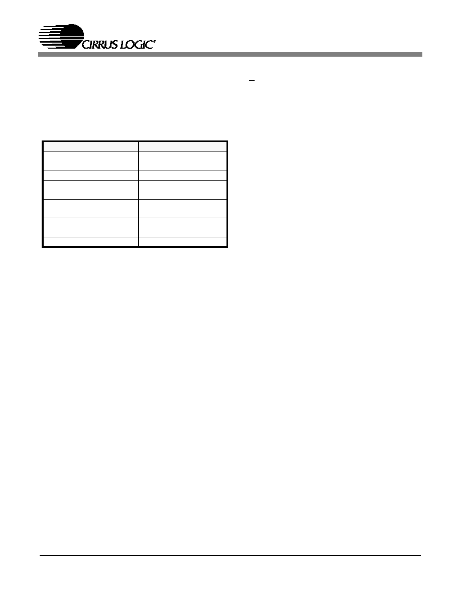
CS61884
DS485PP4
53
18.1 Transformer specifications
Recommended
transformer
specifications
are
shown in
Table 12
. Any transformer used with the
CS61884 should meet or exceed these specifica-
tions.
18.2 Crystal Oscillator Specifications
When a reference clock signal is not available, a
CMOS crystal oscillator may be used as the refer-
ence clock signal. The oscillator must have a mini-
mum symmetry of 40-60% and minimum stability
of + 100ppm for both E1 and T1/J1 applications.
18.3 Designing for AT&T 62411
For information on requirements of the AT&T
62411 and the design of the appropriate system
synchronizer, refer to Application Note AN012
"AT&T 62411 Design Considerations - Jitter and
Synchronization" and Application Note AN011
"Jitter Testing Procedures for Compliance with
AT&T 62411".
18.4 Line Protection
Secondary protection components can be added to
the line interface circuitry to provide lightning
surge and AC power-cross immunity. For addition-
al information on the different electrical safety
standards and specific applications circuit recom-
mendations, refer to Application Note AN034
"Secondary Line Protection for T1 and E1 Cards".
Table 12. Transformer Specifications
Descriptions
Specifications
Turns Ratio Receive/Trans-
mit
1:2
Primary Inductance
1.5mH min. @ 772 kHz
Primary Leakage Induc-
tance
0.3
µH max @ 772 kHz
Secondary leakage Induc-
tance
0.4
µH max @ 772 kHz
Inter winding Capacitance
18pF max, primary to
secondary
ET-Constant
16V -
µs min.
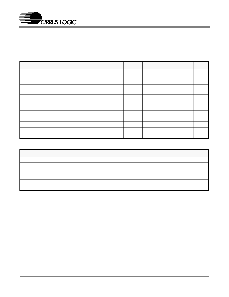
CS61884
54
DS485PP4
19. CHARACTERISTICS AND SPECIFICATIONS
19.1 Absolute Maximum Ratings
CAUTION: Operations at or beyond these limits may result in permanent damage to the device. Normal operation
is not guaranteed at these extremes.
19.2 Recommended Operating Conditions
Notes: 1. Human Body Model
2. Transient current of up to 100 mA will not cause SCR latch-up. Also TTIP, TRING, TV+ and TGND can
withstand a continuous current of 100 mA.
3. Power consumption while driving line load over the full operating temperature and power supply voltage
range. Includes all IC channels and loads. Digital inputs are within 10% of the supply rails and digital
outputs are driving a 50pF capacitive load.
4. Typical consumption corresponds to 50% ones density for E1/T1/J1 modes and medium line length
setting for T1/J1 mode at 3.3Volts.
5. Maximum consumption corresponds to 100% ones density for E1/T1/J1 modes and maximum line
length settings for T1/J1 mode at 3.465Volts.
6. This specification guarantees TTL compatibility (V
OH
= 2.4 V @ I
OUT
= -400
µA).
7. Output drivers are TTL compatible.
8. Pulse amplitude measured at the output of the transformer across a 75
load.
9. Pulse amplitude measured at the output of the transformer across a 120
load.
10. Pulse amplitude measured at the output of the transformer across a 100
load for all line length
settings.
Parameter
Symbol
Min.
Max
Units
DC Supply
(referenced to RGND = TGND = 0V)
RV+
TV+
-
-
4.0
4.0
V
V
DC Supply
VCCIO
-0.5
4.6
V
Input Voltage, Any Digital Pin except CBLSEL, MODE and
LOOP(n) pins
(referenced to GNDIO = 0V)
V
IH
GNDIO -0.5
5.3
V
Input Voltage CBLSEL, MODE & LOOP(n) Pins
(referenced to GNDIO = 0V)
V
IH
GNDIO -0.5
VCCIO +0.5
V
Input voltage, RTIP and RRING Pins
TGND -0.5
TV+ +0.5
V
ESD voltage, Any pin
Note
1
2k
-
V
Input current, Any Pin
Note
2
I
IH
-10
+10
mA
Maximum Power Dissipation, In package
P
p
-
1.73
W
Ambient Operating Temperature
T
A
-40
85
C
Storage Temperature
T
stg
-65
150
C
Parameter
Symbol
Min.
Typ
Max
Units
DC Supply
RV+, TV+
3.135
3.3
3.465
V
DC Supply
VCCIO
3.135
3.3
3.465
V
Ambient operating Temperature
T
A
-40
25
85
C
Power Consumption, T1/J1 Mode, 100
line load
Notes
3
,
4
,
5
-
-
970
1900
mW
Power Consumption, E1 Mode, 75
line load
Notes
3
,
4
,
5
-
-
810
1400
mW
Power Consumption, E1 Mode, 120
line load
Notes
3
,
4
,
5
-
-
750
1300
mW
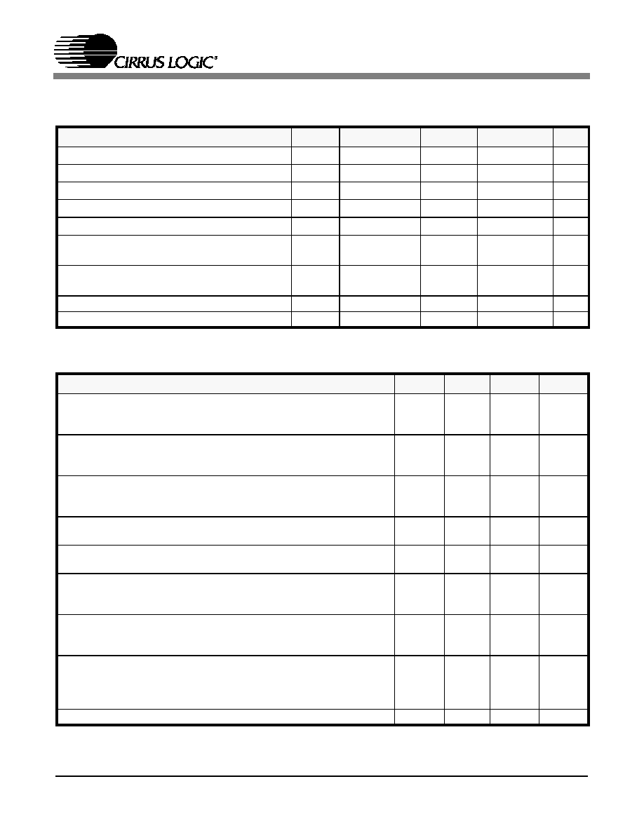
CS61884
DS485PP4
55
19.3 Digital Characteristics
(TA = -40
∞C to 85∞C; TV+, RV+ = 3.3 V ±5%; GND = 0 V)
19.4 Transmitter Analog Characteristics
(TA = -40
∞C to 85∞C; TV+, RV+ = 3.3 V ±5%; GND = 0 V)
Parameter
Symbol
Min.
Typ
Max
Units
High-Level Input Voltage
Note
6
V
IH
2.0
-
-
V
Low-Level Input Voltage
Note
6
V
IL
-
-
0.8
V
LOOP[7:0] Low-Level Input Voltage
V
IHL
-
-
1/3 VCCIO-0.2
V
LOOP[7:0] Mid-Level Input Voltage
V
IHM
1/3 VCCIO +0.2 1/2 VCCIO 2/3 VCCIO-0.2
V
LOOP[7:0] High-Level Input Voltage
V
IHH
2/3 VCCIO +0.2
-
-
V
High-Level Output Voltage
Notes
6
,
7
I
OUT
= -400
µA
V
OH
2.4
-
-
V
Low-Level Output Voltage
Notes
6
,
7
I
OUT
= 1.6 mA
V
OL
-
-
0.4
V
Input Leakage Current
-10
-
+10
µA
Input leakage for LOOP pins
-150
-
+150
µA
Parameter
Min.
Typ
Max
Units
Output Pulse Amplitudes
E1 75
Notes
8
,
9
,
10
E1 120
T1/J1
100
2.14
2.7
2.4
2.37
3.0
3.0
2.6
3.3
3.6
V
V
V
Ratio of Positive to Negative pulses
T1/J1 100
Notes
8
,
9
,
10
E1, amplitude at center of pulse interval
E1, width at 50% of nominal amplitude
0.95
0.95
0.95
-
-
-
1.05
1.05
1.05
Pulse Amplitude of a space
T1/J1 100
E1 120
E1 75
-0.15
-0.3
-0.237
-
-
-
0.15
0.3
0.237
V
V
V
Power in 2 kHz band about 772 kHz
Notes
11
,
12
(T1/J1 100
only)
12.6
-
-
dBm
Power in 2 kHz band about 1.544 MHz
Notes
11
,
12
(referenced to power in 2 kHz band at 772 kHz, T1/J1 100
only)
-29
-
-
dBm
Transmit Return Loss - E1
51 kHz to 102 kHz
102 kH to 2048 kHz
Notes
11
,
12
,
13
2048 kHz to 3072 kHz
- 14
- 14
- 14
- 20
- 19
- 18
-
-
-
dB
Transmit Return Loss - T1/J1
51 kHz to 102 kHz
102 kHz to 2048 kHz
Notes
11
,
12
,
13
2048 kHz to 3072 kHz
- 14
- 14
- 14
- 19
- 19
- 18
-
-
-
dB
Jitter Added by the Transmitter
10 Hz - 8 kHz
8 kHz - 40 kHz
Notes
11
,
14
10 Hz - 40 kHz
Broad Band
-
-
-
-
0.010
0.009
0.007
0.015
0.020
0.025
0.025
0.050
UI
Transmitter Short Circuit Current per channel
-
-
50
mA RMS

CS61884
56
DS485PP4
19.5 Receiver Analog Characteristics
(TA = -40
∞C to 85∞C; TV+, RV+ = 3.3 V ±5%; GND = 0 V))
Notes: 11. Parameters guaranteed by design and characterization.
12. Using components on the CDB61884 evaluation board in Internal Match Impedance Mode.
13. Return loss = 20log10 ABS((Z1 + Z0) / (Z1 - Z0)) where Z1 - impedance of the transmitter or receiver,
and Z0 = cable impedance.
14. Assuming that jitter free clock is input to TCLK.
15. Jitter tolerance for 0 dB for T1/J1 input signal levels and 6 dB for E1 input signal levels. Jitter tolerance
increases at lower frequencies. HDB3/B8ZS coders enabled.
16. In Data Recovery Mode.
17. Jitter Attenuator in the receive path.
Parameter
Min.
Typ
Max
Units
Allowable Cable Attenuation @ 1024kHz and 772kHz
-
-
- 12
dB
RTIP/RRING Input Impedance
T1/J1 100
Load
(Internal Line matching mode)
E1 120
Load
Note
11
E1 75
Load
-
-
-
140
14k
50
-
-
-
RTIP/RRING Input Impedance
T1/J1 100
Load
(External Line matching mode)
E1 120
Load
Note
11
E1 75
Load
-
-
-
14K
14k
14K
-
-
-
Receiver Dynamic Range
0.5
-
-
Vp
Signal to Noise margin (Per G.703, O151 @ 6dB cable Atten).
Note
11
-
- 18
-
dB
Receiver Squelch Level
-
150
-
mV
LOS Threshold
-
200
-
mV
LOS Hysteresis
-
50
-
mV
Data Decision Threshold
E1 Modes
Note
11
41
50
59
% of
peak
Data Decision Threshold
T1/J1 Modes
Note
11
56
65
74
% of
peak
Input Jitter Tolerance - E1
1 Hz - 1.8 Hz
Notes
11
,
15
,
17
20 Hz - 2.4 kHz
18 kHz - 100 kHz
18
1.5
0.2
-
-
-
-
-
-
UI
Input Jitter Tolerance - T1/J1
0.1 Hz - 1 Hz
Notes
11
,
15
,
17
4.9 Hz - 300 kHz
10kHz - 100 kHz
138
28
0.4
-
-
-
-
-
-
UI
Input Return Loss - E1/T1/J1
51 kHz - 102 kHz
102 kHz - 2048 kHz
Notes
11
,
12
,
13
2048 kHz - 3072 kHz
- 18
- 18
- 18
- 28
- 30
- 27
-
-
-
dB

CS61884
DS485PP4
57
19.6 Jitter Attenuator Characteristics
(TA = -40
∞C to 85∞C; TV+, RV+ = 3.3 V ±5%; GND = 0 V)
Notes: 18. Attenuation measured with sinusoidal input filter equal to 3/4 of measured jitter tolerance. Circuit
attenuates jitter at 20 dB/decade above the corner frequency. Output jitter can increase significantly
when more than 28 UI's are input to the attenuator.
19. Measurement is not effected by the position of the Jitter Attenuator.
Parameter
Min.
Typ
Max
Units
Jitter Attenuator Corner Frequency
T1/J1 Modes
Note
11
,
19
T1/J1 Modes
E1 Modes
(Depends on JACF Bit in host mode)
E1 Modes
-
-
-
-
3.78
7.56
1.25
2.50
-
-
-
-
Hz
E1 Jitter Attenuation
3 Hz to 40 Hz
Note
11
,
18
400 Hz to 100 kHz
+ 0.5
- 19.5
-
-
-
-
dB
T1/J1 Jitter Attenuation
1 Hz to 20 Hz
1 kHz
Note
11
,
18
1.4KHz to 100KHz
0
- 33.3
- 40
-
-
-
-
-
-
dB
Attenuator Input Jitter Tolerance before FIFO
32-bit FIFO
over flow and under flow
Note
11
64-bit FIFO
-
-
24
56
-
-
UI
UI
Delay through Jitter Attenuator Only
32-bit FIFO
Note
11
64-bit FIFO
-
-
16
32
-
-
UI
UI
Intrinsic Jitter in Remote Loopback
Notes
11
,
17
-
-
0.11
UI
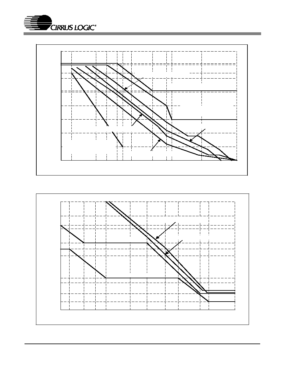
CS61884
58
DS485PP4
1
10
100
1K
10K
0
A
t
t
e
nuat
i
on
i
n
dB
Frequency in Hz
+ 0.5
2
57
1.4K
20
400
40
+ 10
- 10
- 20
- 30
- 50
- 40
- 60
- 19.5
- 6
- 70
100K
AT&T 62411
Minimum Attenuation
ITU G.736
TYP. T1 @ 3.78Hz CF
TYP. E1 @ 1.25 Hz CF
TYP. E1 @ 2.5 Hz CF
TYP. T1 @ 7.56Hz CF
AT&T 62411
Maximum Attenuation
Figure 19. Jitter Transfer Characteristic vs. G.736, TBR 12/13 & AT&T 62411
PEAK
T
O
PEAK
J
I
TTER
(
UI
)
FREQUENCY IN Hz
1
10
1k
100
100k
1.8
4.9
20
300
10k
2.4k
18k
1
.1
10
100
.2
.4
1.5
1000
18
28
138
300
AT&T 62411
ITU G.823
TYP. E1 Performance
TYP. T1 Performance
Figure 20. Jitter Tolerance Characteristic vs. G.823 & AT&T 62411
CS61884
DS485PP4
59
19.7 Master Clock Switching Characteristics
19.8 Transmit Switching Characteristics
19.9 Receive Switching Characteristics
* All parameters guaranteed by production, characterization or design.
Notes: 20. Output load capacitance = 50pF.
21. MCLK is not active.
22. Parameters guaranteed by design and characterization.
Parameter
Symbol
Min.
Typ
Max
Units
MASTER CLOCK (MCLK)
Master Clock Frequency
E1 Modes
MCLK
2.048
MHz
Master Clock Frequency
T1/J1 Modes
MCLK
1.544
MHz
Master Clock Tolerance
-
-100
+100
ppm
Master Clock Duty Cycle
-
40
50
60
%
Parameter
Symbol
Min.
Typ
Max
Units
E1 TCLK Frequency
1/t
pw2
-
2.048
-
MHz
E1 TPOS/TNEG Pulse Width (RZ Mode)
236
244
252
nS
T1/J1 TCLK Frequency
1/t
pw2
-
1.544
-
MHz
TCLK Tolerance (NRZ Mode)
-50
-
50
PPM
TCLK Duty Cycle
t
pwh2
/t
pw2
-
-
90
%
TCLK Pulse Width
20
-
-
nS
TCLK Burst Rate
Note
22
-
-
20
MHz
TPOS/TNEG to TCLK Falling Setup Time (NRZ Mode)
t
su2
25
-
-
nS
TCLK Falling to TPOS/TNEG Hold time (NRZ Mode)
t
h2
25
-
-
nS
TXOE Asserted Low to TX Driver HIGH-Z
-
-
1
µS
TCLK Held Low to Driver HIGH-Z
Note
21
8
12
20
µS
Parameter
Symbol
Min.
Typ
Max
Units
RCLK Duty Cycle
40
50
60
%
E1 RCLK Pulse Width
196
244
328
nS
E1 RPOS/RNEG Pulse Width (RZ Mode
200
244
300
nS
E1 RPOS/RNEG to RCLK rising setup time
t
su
150
244
-
nS
E1 RPOS/RNEG to RCLK hold time
t
h
200
244
-
nS
T1/J1 RCLK Pulse Width
259
324
388
nS
T1/J1 RPOS/RNEG Pulse Width (RZ Mode)
250
324
400
nS
T1/J1 POS/RNEG to RCLK rising setup time
t
su
150
324
-
nS
T1/J1 RPOS/RNEG to RCLK hold time
t
h
200
324
-
nS
RPOS/RNEG Output to RCLK Output (RZ Mode)
-
-
10
nS
Rise/Fall Time, RPOS, RNEG, RCLK, LOS outputs
t
r
, t
f
-
-
85
nS
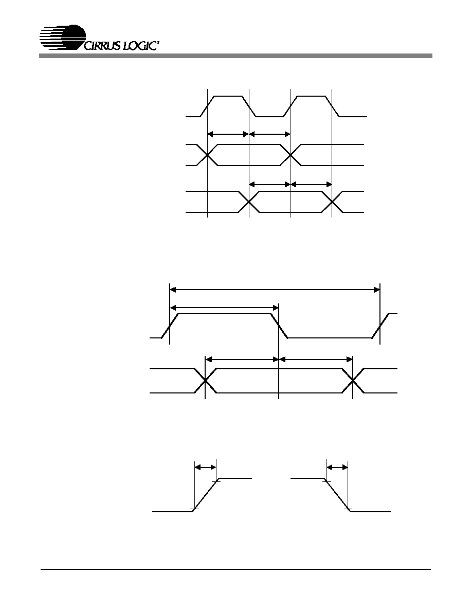
CS61884
60
DS485PP4
RCLK
t
su
RPOS/RNEG
CLKE = 1
t
su
t
h
t
h
RPOS/RNEG
CLKE = 0
Figure 21. Recovered Clock and Data Switching Characteristics
TPOS/TNEG
TCLK
t
pw2
t
pwh2
t
su2
t
h2
Figure 22. Transmit Clock and Data Switching Characteristics
Any Digital Output
10%
90%
t r
t f
10%
90%
Figure 23. Signal Rise and Fall Characteristics
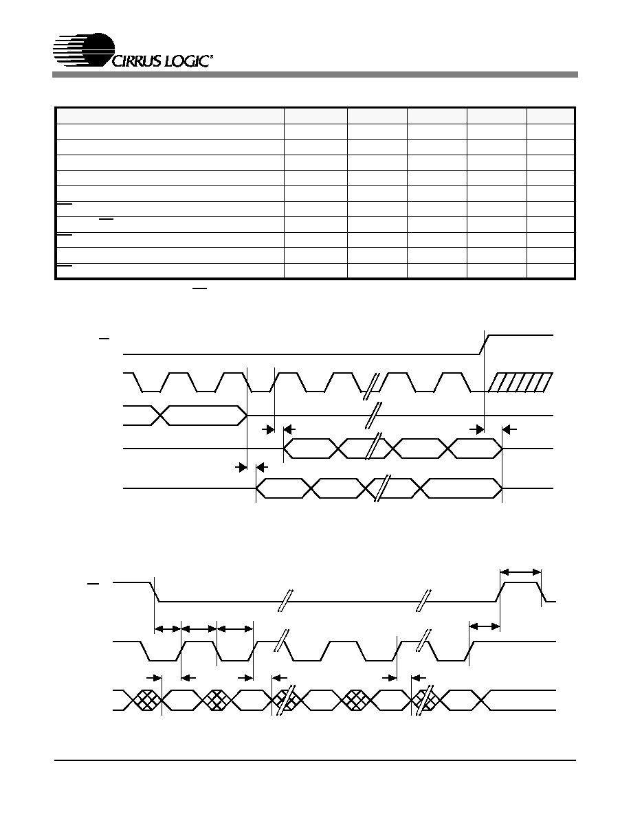
CS61884
DS485PP4
61
19.10 Switching Characteristics - Serial Port
Notes: 23. If SPOL = 0, then CS should return high no sooner than 20 ns after the 16
th
rising edge of SCLK during
a serial port read.
Parameter
Symbol
Min.
Typ.
Max
Unit
SDI to SCLK Setup Time
t
dc
-
20
-
ns
SCLK to SDI Hold Time
t
cdh
-
20
-
ns
SCLK Low Time
t
cl
-
50
-
ns
SCLK High Time
t
ch
-
50
-
ns
SCLK Rise and Fall Time
t
r
, t
f
-
15
-
ns
CS to SCLK Setup Time
t
cc
-
20
-
ns
SCLK to CS Hold Time
Note
23
t
cch
-
20
-
ns
CS Inactive Time
t
cwh
-
70
-
ns
SDO Valid to SCLK
Note
23
t
cdv
-
60
-
ns
CS to SDO High Z
t
cdz
-
50
-
ns
CS
SDI
SCLK
SDO
CLKE=1
LAST ADDR BIT
SDO
CLKE=0
HIGH Z
t
cdv
t
cdv
t
cdz
D0
D1
D0
D6
D1
D6
D7
D7
Figure 24. Serial Port Read Timing Diagram
CS
SCLK
t
cc
SDI
LSB
LSB
MSB
t
ch
t
cl
t
cch
t
cwh
t
dc
t
cdh
t
cdh
Figure 25. Serial Port Write Timing Diagram
CS61884
62
DS485PP4
19.11 Switching Characteristics - Parallel Port (Multiplexed Mode)
* All paramters guaranteed by production, characterization or design.
Parameter
Ref. #
Min.
Typ.
Max
Unit
Pulse Width AS or ALE High
1
25
-
-
ns
Muxed Address Setup Time to AS or ALE Low
2
10
-
-
ns
Muxed Address Hold Time
3
5
-
-
ns
Delay Time AS or ALE to WR, RD or DS
4
5
-
-
ns
CS & R/W Setup Time Before WR, RD or DS Low
5
0
-
-
ns
CS & R/W Hold Time
6
0
-
-
ns
Pulse Width, WR, RD, or DS
7
70
-
-
ns
Write Data Setup Time
8
30
-
-
ns
Write Data Hold Time
9
30
-
-
ns
Output Data Delay Time from RD or DS Low
10
-
-
100
ns
Read Data Hold Time
11
5
-
-
ns
Delay Time WR, RD, or DS to ALE or AS Rise
12
30
-
-
ns
WR or RD Low to RDY Low
13
-
-
55
ns
WR or RD Low to RDY High
14
-
-
100
ns
WR or RD High to RDY HIGH-Z
15
-
-
40
ns
DS Low to ACK High
16
-
-
65
ns
DS Low to ACK Low
17
-
-
100
ns
DS High to ACK HIGH-Z
18
-
-
40
ns

CS61884
DS485PP4
63
ALE
W R
D[7:0]
RDY
HIGH-Z
HIGH-Z
C S
1
12
4
7
6
9
8
3
5
2
13
15
14
ADDRESS
Write Data
Figure 26. Parallel Port Timing - Write; Intel Multiplexed Address / Data Bus Mode
ALE
R D
D[7:0]
RDY
HIGH-Z
HIGH-Z
C S
1
12
4
7
6
3
5
2
13
15
14
11
10
ADDRESS
Read Data
Figure 27. Parallel Mode Port Timing - Read; Intel Multiplexed Address / Data Bus Mode

CS61884
64
DS485PP4
D[7:0]
R/W
DS
AS
Write Data
HIGH-Z
HIGH-Z
ADDRESS
1
5
2
4
3
16
17
18
7
6
CS
8
12
9
ACK
Figure 28. Parallel Port Timing - Write in Motorola Multiplexed Address / Data Bus
D[7:0]
R/W
DS
AS
Read Data
HIGH-Z
HIGH-Z
ADDRESS
1
5
2
4
3
16
17
18
7
6
CS
10
12
11
ACK
Figure 29. Parallel Port Timing - Read in Motorola Multiplexed Address / Data Bus
CS61884
DS485PP4
65
19.12 Switching Characteristics- Parallel Port (Non-multiplexed Mode)
* All paramters guaranteed by production, characterization or design.
Parameter
Ref. #
Min.
Typ.
Max
Unit
Address Setup Time to WR, RD or DS Low
1
10
-
-
ns
Address Hold Time
2
5
-
-
ns
CS & R/W Setup Time Before WR, RD or DS Low
3
0
-
-
ns
CS & R/W Hold Time
4
0
-
-
ns
Pulse Width, WR, RD, or DS
5
70
-
-
ns
Write Data Setup Time
6
30
-
-
ns
Write Data Hold Time
7
30
-
-
ns
Output Data Delay Time from RD or DS
8
-
-
100
ns
Read Data Hold Time
9
5
-
-
ns
WR or RD Low to RDY Low
10
-
-
55
ns
WR, RD or DS Low to RDY High
11
-
-
100
ns
WR, RD or DS High to RDY HIGH-Z
12
-
-
40
ns
DS Low to ACK High
13
-
-
65
ns
DS Low to ACK Low
14
-
-
100
ns
DS High to ACK HIGH-Z
15
-
-
40
ns

CS61884
66
DS485PP4
A[4:0]
D[7:0]
ALE
RDY
WR
(pulled high)
CS
HIGH-Z
1
7
10
HIGH-Z
11
12
2
5
3
4
6
ADDRESS
Write Data
Figure 30. Parallel Port Timing - Write in Intel Non-Multiplexed Address / Data Bus Mode
A[4:0]
D[7:0]
ALE
RDY
RD
(pulled high)
CS
HIGH-Z
1
9
10
HIGH-Z
11
12
2
5
3
4
8
ADDRESS
Read Data
Figure 31. Parallel Port Timing - Read in Intel Non-Multiplexed Address / Data Bus Mode

CS61884
DS485PP4
67
(pulled high)
HIGH-Z
1
7
13
HIGH-Z
14
15
2
5
3
4
6
ADDRESS
Write Data
ACK
D[7:0]
CS
R/W
DS
AS
A[4:0]
Figure 32. Parallel Port Timing - Write in Motorola Non-Multiplexed Address / Data Bus Mode
A[4:0]
D[7:0]
CS
(pulled high)
DS
HIGH-Z
1
9
HIGH-Z
14
15
2
5
3
4
8
ADDRESS
Read Data
AS
ACK
R/W
13
Figure 33. Parallel Port Timing - Read in Motorola Non-Multiplexed Address / Data Bus Mode
CS61884
68
DS485PP4
19.13 Switching Characteristics - JTAG
Parameter
Symbol
Min.
Max
Units
Cycle Time
t
cyc
200
-
nS
TMS/TDI to TCK Rising Setup Time
t
su
50
-
nS
TCK Rising to TMS/TDI Hold Time
t
h
50
-
nS
TCK Falling to TDO Valid
t
dv
-
70
nS
TCK
TMS
TDI
TDO
t
su
t
h
t
cyc
t
dv
Figure 34. JTAG Switching Characteristics

CS61884
DS485PP4
69
20. COMPLIANT RECOMMENDATIONS AND SPECIFICATIONS
AT&T Pub 62411
FCC Part 68
ANSI T1.102
ANSI T1.105
ANSI T1.231
ANSI T1.403
ANSI T1.408
Bell Core TR-TSY-000009
Bell Core GR-253-Core Sonet
Bell Core GR-499-Core
ETSI ETS 300-011
ETSI ETS 300-166
ETSI ETS 300-233
IEEE 1149.1
ETSI TBR 12/13
ITU-T I.431
ITU-T G.703
ITU-T G.704
ITU-T G.706
ITU-T G.732
ITU-T G.735
ITU-T G.736
ITU-T G.742
ITU-T G.772
ITU-T G.775
ITU-T G.783
ITU-T G.823
ITU-T O.151
OFTEL OTR-001
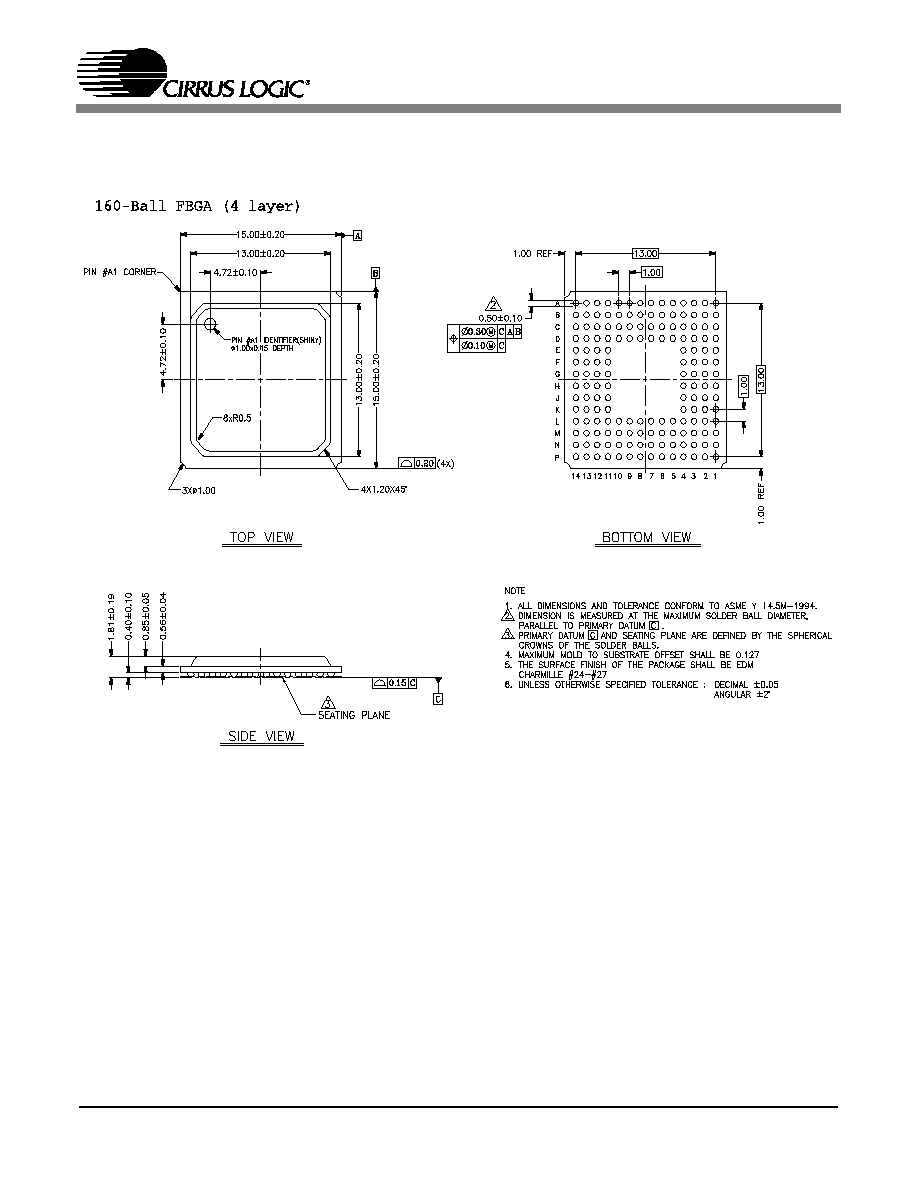
CS61884
70
DS485PP4
21. FBGA PACKAGE DIMENSIONS

CS61884
DS485PP4
71
22. LQFP PACKAGE DIMENSIONS
INCHES
MILLIMETERS
DIM
MIN
NOM
MAX
MIN
NOM
MAX
A
---
0.55
0.063
---
1.40
1.60
A1
0.002
0.004
0.006
0.05
0.10
0.15
B
0.007
0.008
0.011
0.17
0.20
0.27
D
0.854
0.866 BSC
0.878
21.70
22.0 BSC
22.30
D1
0.783
0.787 BSC
0.791
19.90
20.0 BSC
20.10
E
0.854
0.866 BSC
0.878
21.70
22.0 BSC
22.30
E1
0.783
0.787 BSC
0.791
19.90
20.0 BSC
20.10
e*
0.016
0.020
0.024
0.40
0.50 BSC
0.60
0.000∞
4∞
7.000∞
0.00∞
4∞
7.00∞
L
0.018
0.024
0.030
0.45
0.60
0.75
* Nominal pin pitch is 0.50 mm
Controlling dimension is mm.
JEDEC Designation: MS022
144L LQFP PACKAGE DRAWING
E1
E
D1
D
1
e
L
B
A1
A
