| –≠–ª–µ–∫—Ç—Ä–æ–Ω–Ω—ã–π –∫–æ–º–ø–æ–Ω–µ–Ω—Ç: CS7615-KQ | –°–∫–∞—á–∞—Ç—å:  PDF PDF  ZIP ZIP |
Document Outline
- CS7615
- Features
- Description
- TABLE OF CONTENTS
- SPECIFICATIONS & CHARACTERISTICS
- ANALOG CHARACTERISTICS:
- DIGITAL CHARACTERISTICS:
- POWER CONSUMPTION:
- CONTROL PORT CHARACTERISTICS:
- Figure 1. I2C Timing Diagram
- SWITCHING CHARACTERISTICS:
- RECOMMENDED OPERATING CHARACTERISTICS:
- ABSOLUTE MAXIMUM RATINGS:
- GENERAL DESCRIPTION
- Overview
- Figure 3. Typical 4-Chip Digital CCD Camera
- Interfacing the CS7615 with CS7665 or CS7666
- Figure 4. CS7615/CS7665 Interface
- Figure 5. CS7615/CS7666 Interface
- Operation
- Figure 6. CS7615 Output Data Format
- Figure 7. CS7615 Output Data and Clocks
- CCD Timing Generator
- Vertical Timing Specifications
- Table 1. CCD vertical timing specifications
- Figure 8. Vertical Shift Register Signal Timings for Charge Read Out Phase
- Horizontal Timing Specifications
- Table 2. Horizontal timing specifications
- Figure 9. Timing Diagram for Href, HSYNC, Clamp, and Henb
- Figure 10. Vertical Shift Register Signal Timings
- Figure 11. Vertical Shift Register Signal Timings for Charge Read Out Phase
- Figure 12. Charge Read Out Signal Timing
- Figure 13. Electronic Shutter Control Signal Timing
- Description of Operation
- Automatic Gain Control
- Correlated Double Sampling (CDS)
- Analog to Digital Converter
- Black Level Adjust to Code 16 (10-bit Code 64)
- Formatter
- SERIAL CONTROL BUS
- Station Address
- Write Operations
- Table 3. WRITE Format Packet
- Address Set Operation
- Table 4. ADDRESS SET Format Packet Operation
- Read Operations
- Table 5. READ Format Packet.
- REGISTER DESCRIPTIONS
- Low Power Register (20h)
- Operational control #1 Register (24h)
- Gain Registers (25-26h)
- AGC Error Statistic Register (27h):
- AGC Count Statistic Register (28h)
- AGC Target Value Register (29h)
- AGC Maximum Gain Register (2Ah)
- AGC Slew and Speed Register (2Bh)
- AGC Minimum Gain Register (2Ch)
- CCD Signal Alignment Register (2Dh)
- VRST Registers (2Eh, 2Fh)
- Maximum Shutter Exposure Register (30h)
- Operational Control #2 Register (31h)
- Timing Control- Line Number Registers (33h-39h)
- Timing Control-Horizontal Blank Pd Register (40h)
- Timing Control- Line Length Register (41h-42h)
- Timing Control- HSYNC Registers (43h-44h)
- Timing Control - Black Clamp Register (45h)
- Timing Control - HENB Registers (46h-47h)
- Timing Control - V1X Registers (48h-49h)
- Timing Control - V2X Registers (4Ah-4Bh)
- Timing Control - V3X Registers (4Ch-4Dh)
- Timing Control - V4X Registers (4Eh-4Fh):
- Timing Control - Charge Read Out in Odd Field V2X Registers (50h-52h)
- Timing Control - Charge Read Out in Odd Field V3X Registers (53h-55h)
- Timing control - Charge Read Out in Even Field V2X Registers (56h-58h)
- Timing Control - Charge Read Out in Even Field V3X Registers (59h-5Bh)
- Timing Control - Charge Read Out in Even Field V4X Registers (5Ch-5Eh)
- Timing Control - H1X Registers (5Fh-61h)
- Timing Control - VH1X Registers (62h-64h)
- Black Level Adjust Register (68h)
- Version (Minor) Register (69h)
- Version (Major) Register (6Ah)
- Station Address Register (FEh)
- Pin Descriptions
- Power Supply Connections
- Analog Input
- Digital Inputs
- Timing Generator Outputs
- Mosaic Data and clock Outputs
- Table 6. Digital Mosaic Outputs.
- I 2 C Serial Control
- PACKAGE DIMENSIONS

Preliminary Product Information
This document contains information for a new product.
Cirrus Logic reserves the right to modify this product without notice.
1
Copyright
©
Cirrus Logic, Inc. 1998
(All Rights Reserved)
Cirrus Logic, Inc.
Crystal Semiconductor Products Division
P.O. Box 17847, Austin, Texas 78760
(512) 445 7222 FAX: (512) 445 7581
http://www.crystal.com
CS7615
CCD Imager Analog Processor
Features
l
10-Bit A/D Converter
l
Multi-Sync CCD Timing Generator,
handles imagers up to 1000 pixels wide
l
Integrated Correlated Double Sampler
l
38 dB Automatic Analog Gain Control
l
Up to 90 dB Total Gain Adjust Range
l
Closed-Loop "Fuzzy" AGC/Exposure
l
Code 16 Black Level Clamp
l
I
2
C Control Bus
l
4-Phase Vertical CCD Timing Signals
l
No CCD Buffer Amplifier Required
l
Master Clock or Crystal Controlled
Description
The CS7615 is a low-power Analog front-end processor
for standard four-color interline transfer CCD imagers.
The architecture includes a correlated double sampler,
AGC amplifier, black-level clamp, 10-Bit A/D converter,
and a complete multi-sync CCD timing generator. The
analog CCD imager output can be directly connected to
the CS7615 input, which does not require an external
buffer amplifier. The pixel data is double sampled for im-
proved noise performance, and gain adjusted prior to
being digitized by the A/D converter. Feedback from the
A/D converter holds the image black level at code-16
(assumes 8-bit data path), addressing ITU-601 compli-
ance issues. The multi-sync CCD timing generator is
programmed via the I
2
C bus, and can be used with a
wide range of interline transfer CCD imagers up to 1000
pixels wide. The CS7615 supports full ITU-601 compli-
ance for images up to 720 pixels wide, and is compatible
with both NTSC and PAL timing. The CS7615 is de-
signed to be used along with either the CS7665 or
CS7666 Digital Color-Space Processor for CCD Camer-
as, which generates a 4:2:2 component digital video
output.
ORDERING INFORMATION
CS7615-KQ
0∞ to +70∞ C
44-pin TQFP
(10 mm ◊ 10 mm ◊ 1.6 mm)
CCD Output
Master Clock
CDS/AGC
Data Out
PLL
Output
Register
I
2
C
Block
Formatter
A/D
Converter
Black
Level
Timing
Generator
AGC
Controller
CCD Timing Signals
I
2
C Bus
Clocks Out
JUL `98
DS231PP6

CS7615
2
DS231PP6
TABLE OF CONTENTS
ANALOG CHARACTERISTICS: ........................................................................... 3
DIGITAL CHARACTERISTICS: ............................................................................ 3
POWER CONSUMPTION: .................................................................................... 3
CONTROL PORT CHARACTERISTICS: .............................................................. 4
SWITCHING CHARACTERISTICS: ...................................................................... 5
RECOMMENDED OPERATING CHARACTERISTICS: ....................................... 5
ABSOLUTE MAXIMUM RATINGS: ....................................................................... 5
GENERAL DESCRIPTION .................................................................................. 6
Overview ..................................................................................................... 6
Interfacing the CS7615 with CS7665 or CS7666 ....................................... 6
Operation .................................................................................................... 6
CCD Timing Generator ............................................................................... 8
Vertical Timing Specifications ..................................................................... 8
Horizontal Timing Specifications ................................................................. 8
Description of Operation ............................................................................. 9
Automatic Gain Control ............................................................................... 9
Correlated Double Sampling (CDS) .......................................................... 11
Analog to Digital Converter ....................................................................... 15
Black Level Adjust to Code 16 (10-bit Code 64) ....................................... 15
Formatter .................................................................................................. 15
SERIAL CONTROL BUS ................................................................................... 16
Station Address ........................................................................................ 16
Write Operations ................................................................................ 16
Address Set Operation ....................................................................... 16
Read Operations ................................................................................ 16
REGISTER DESCRIPTIONS ............................................................................. 17
PIN DESCRIPTIONS ......................................................................................... 30
PACKAGE DIMENSIONS .................................................................................. 34
CS7615
DS231PP6
3
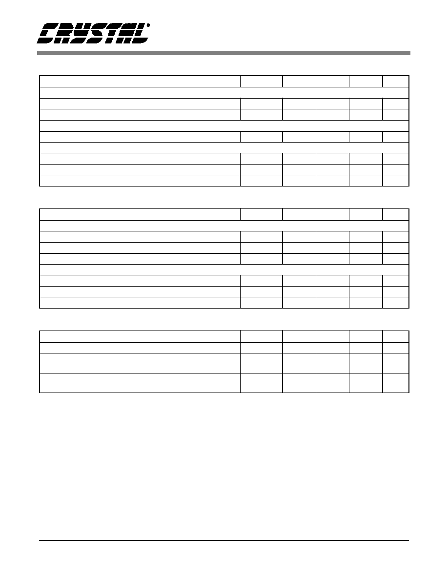
ANALOG CHARACTERISTICS:
(T
A
=25∞ C; V
AA
=V
DD
=5V; Output Load=30pF )
DIGITAL CHARACTERISTICS:
(T
A
=25∞ C; V
AA
=V
DD
=5V; Output Load=30pF )
POWER CONSUMPTION:
(T
A
=25∞ C; V
AA
=V
DD
=5V; Output Load=30pF )
Parameter
Symbol
Min
Typ
Max
Units
Dynamic Performance
Integral Non-Linearity
INL
-
1
-
LSB
Differential Non-Linearity
DNL
-
0.75
-
LSB
Analog Input
Analog Input Capacitance
C
IN
-
10
-
pF
Automatic Gain Control
Maximum Gain
G
MAX
-
20
-
dB
Minimum Gain
G
MIN
-
0
-
dB
Gain Increment
G
-
78.4
117.6
mdB
Parameter
Symbol
Min
Typ
Max
Units
Logic Inputs
High-Level Input Voltage
V
IH
V
DD
-0.8
-
-
V
Low-Level Input Voltage
V
IL
-
-
0.8
V
Input Leakage Current
I
IN
-
-
10
mA
Logic Outputs
High-Level Output Source Current @ V
OH
= V
DD
-0.4V
I
OH
-
-
1
mA
Low-Level Output Sink Current @ V
OL
= 0.4V
I
OL
-
-
1
mA
3-State Leakage Current
I
OZ
-
-
10
µ
A
Parameter
Symbol
Min
Typ
Max
Units
Power Dissipation
P
D
-
650
-
mW
Analog Power Supply Current
Normal Mode
Low-Power Mode
I
AN
I
ALP
-
-
99
63
-
-
mA
mA
DIgital Power Supply Current
Normal Mode
Low-Power Mode
I
DN
I
DLP
-
-
55
22
-
-
mA
mA

CS7615
4
DS231PP6
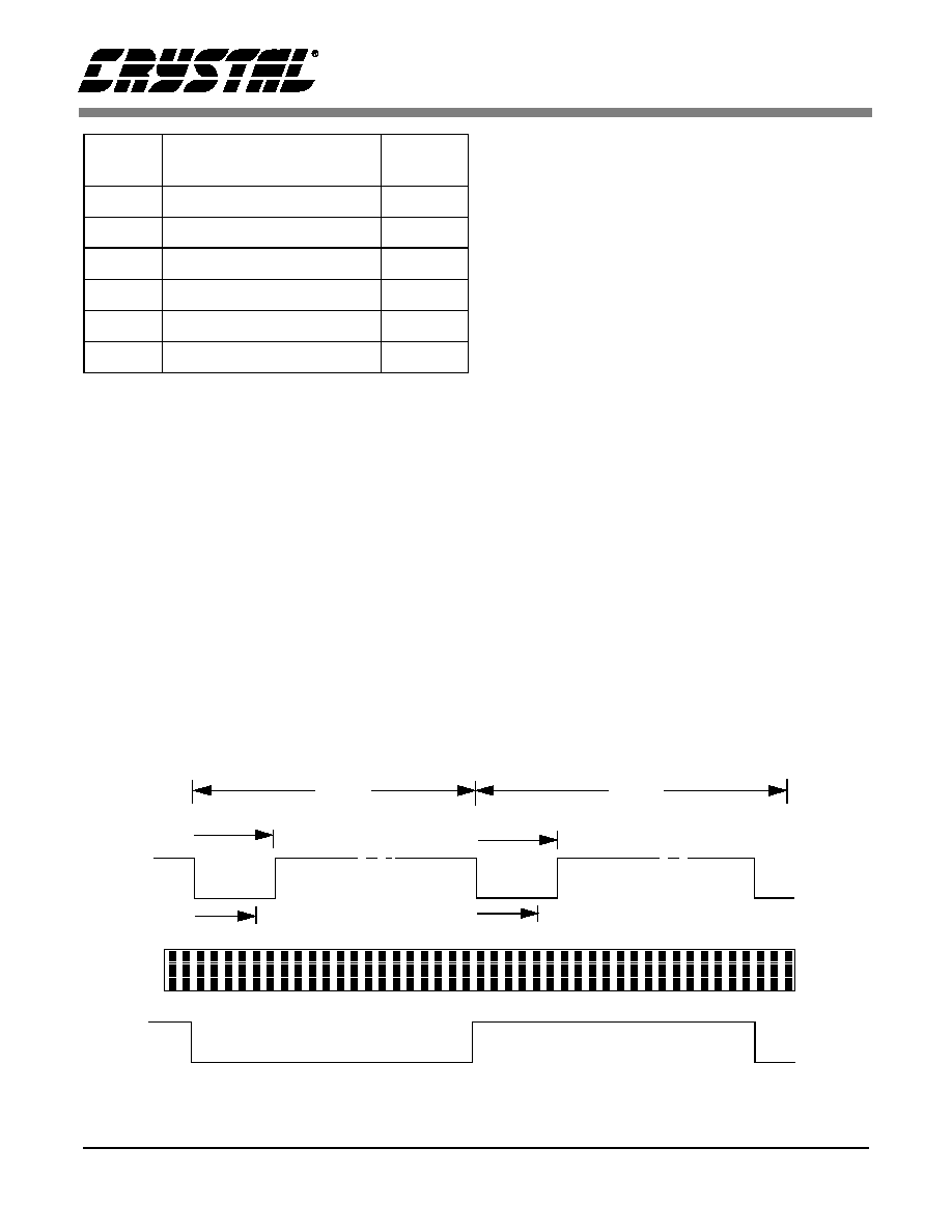
CONTROL PORT CHARACTERISTICS:
(T
A
=25∞ C; V
AA
=V
DD
=5V; Output Load=30pF )
Parameter
Symbol
Min
Typ
Max
Units
SCL Clock Frequency
f
SCL
-
-
100
kHz
Bus Free Time Between Transmissions
t
buf
4.7
-
-
µ
s
Start Condition Hold Time
t
hdst
4.0
-
-
µ
s
Clock Pulse Width
High
Low
t
high
t
low
4.0
4.7
-
-
µ
s
µ
s
Setup TIme for Repeat Start Condition
t
sust
4.7
-
-
µ
s
SDAIN Hold Time from SCL Falling
t
hdd
0
-
-
µ
s
SDAIN Setup Time from SCL Rising
t
sud
0.25
-
-
µ
s
SDAIN and SCL Rise Time
t
r
-
-
1.0
µ
s
SDAIN and SCL Fall Time
t
f
-
-
0.3
µ
s
Setup Time for Stop Condition
t
susp
4.0
-
-
µ
s
t
buf
t
hdst
t hdst
t
low
t
r
t f
t
hdd
t high
t
sud
t
sust
t
susp
Stop
Start
Start
Stop
Repeated
S D A
S C L
Figure 1. I
2
C Timing Diagram

CS7615
DS231PP6
5
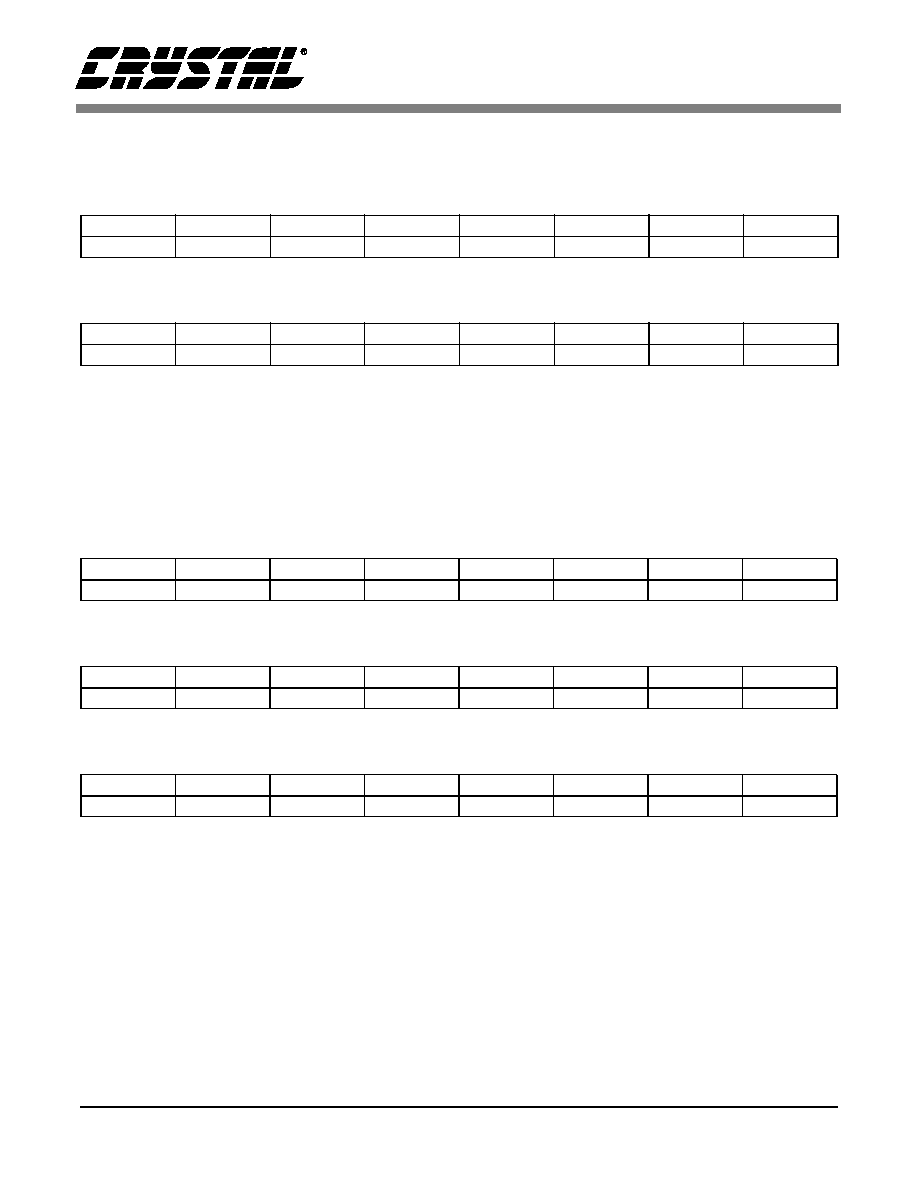
SWITCHING CHARACTERISTICS:
(T
A
=25∞ C; V
SS
=V
DD
=5V; Output Load=30pF )
RECOMMENDED OPERATING CHARACTERISTICS:
ABSOLUTE MAXIMUM RATINGS:
Specifications are subject to change without notice.
Parameter
Symbol
Min
Typ
Max
Units
Crystal Frequency Range
f
CRY
6.75
27
MHz
Crystal Oscillator Duty Cycle
40
60
%
CLKO Frequency
f
pix
6.75
13.5
MHz
CLK2XO Frequency
f
dat
13.5
27
MHz
CLKO duty cycle
50
%
CLK2XO duty cycle
50
%
CLK2XO falling edge to CLKO falling edge
4
8
ns
FR Clock (CCD reset gate clock) Duty Cycle
25
%
H1 Clock
Duty Cycle
50
%
H2 Clock
Duty Cycle
50
%
Parameter
Symbol
Min
Typ
Max
Units
Power Supply Voltage
V
AA
, V
DD
4.5
5.0
5.5
V
GNDA to GNDD Voltage Differential
10
mV
Crystal Frequency Range
6.75
27
MHz
Analog Input AC Range (Figure 2)
V
AC
0
1.65
V
Analog Input DC Offset (Figure 2)
V
DC
12
V
Analog Input Voltage (Figure 2)
A
IN
0
18
V
Parameter
Symbol
Min
Max
Units
Power Supply Voltage
V
AA
, V
DD
-0.3
7.0
V
Digital Input Voltage
GNDD-0.3
(V
DD
)+0.3
V
Analog Input Voltage - AIN only
A
IN
GNDA-(0.3)
20
V
Input Current (except supply pins)
10
mA
Ambient Temperature Range
-0
+70
∞C
Lead Solder Temperature (10sec duration)
+260
∞C
Storage Temperature Range
-65
+150
∞C
GND
V
AIN
V
DC
V
AC
Feedthrough
Level
Figure 2. Analog Input

CS7615
6
DS231PP6
GENERAL DESCRIPTION
Overview
The CS7615 performs the analog functions in a
four chip digital CCD Camera. The four main chips
include the CCD imager, the CS7615 CCD digitiz-
er, the CS7665 or CS7666 color space processor,
and a vertical drive interface-chip for the CCD im-
ager. Several CCD imagers (and their associated
vertical drivers) can be used with the CS7615 digi-
tizer and the CS7665 or CS7666 processor to form
a simple and cost-effective YCrCb output format
digital camera. The block diagram in Figure 3 illus-
trates the system interconnect.
Interfacing the CS7615 with CS7665 or
CS7666
The CS7666 is a direct replacement for the
CS7665. No board or software changes are needed
for existing designs. However, slight changes to
existing hardware and software are necessary to
take advantage of the CS7666. See Figure 4 and 5
and the CS7666 data sheet for more details.
Operation
The CS7615 digitizer is designed to provide all
necessary analog functions and conversion to digi-
tal data of a standard CCD imager output signal as
well as provide all the timing and control signals
for the CCD imager. The architecture includes a
correlated double sampler, variable gain amplifier
with an integrated AGC loop, black level clamp,
10-bit A/D converter, output formatter, and a com-
plete multi-sync CCD timing generator. The output
of the A/D converter ranges from code 004h to
code 3FBh and the formatter adds special end-of-
active-video (EAV) and start-of-active-video
(SAV) codes to each line, making the output of the
CS7615 similar to the description in the ITU-656
recommendation.
CCD
CDS/ADC
IMAGE
PROCESSOR
TIMING
I C
2
I C
2
2
7
9
+5 V
+8 V TO +12 V
DC-DC
CONVERTER
CS7615
CS7665 or CS7666
4:2:2, H.656 VIDEO
I C BUS
2
VERTICAL
DRIVE
512x480
CS4952 or
CS4954
Figure 3. Typical 4-Chip Digital CCD Camera
XTAL
32
33
CS7615
39
4
56
55
CS7665
CLK2x0 CLOCK
CLK0
10-BIT DATA
Figure 4. CS7615/CS7665 Interface
XTAL
33
32 XTALIN
CS7615
39
4
56
52
CS7666
NC
CLK0
10-BIT DATA
55 CLKIN
NC
CCLOKG
Figure 5. CS7615/CS7666 Interface

CS7615
DS231PP6
7
The EAV/SAV code definitions are consistent with
an 8-bit data path. As per the ITU-656 recommen-
dation, the LSB's of the CS7615 are fractional bits
which are not used when delivering 8-bit output da-
ta. In 10-bit mode, all ten digital outputs can be
connected directly to the CS7665.
The output data format from the CS7615 formatter
is shown in Figure 6. The CS7615 also outputs two
clocks, one at the pixel rate and the other at 2◊ the
output pixel data rate (see pin description for
CLK2XO). The output of the formatter is avail-
able at the pins D
O[0..9]
and it transitions at the fall-
ing edge of the pixel rate clock CLKO. Figure 7
shows the basic output timing diagram. The falling
edges of CLKO lag the falling edges of CLK2XO
by 4 to 8 ns and both clocks have approximately
50% duty cycles.
HREF
4T
N
b
T
4T
AV*T
Blanking period
Active video
EAV code (10 bits)
Smpl.
Word
0
3FFh
1
000h
2
000h
3
Binary
1
fv
1
P
3
P
2
P
1
P
0
00
Blank code (10 bits)
Smpl.
Word
4
040h
repeat above word
SAV code (10 bits)
Smpl.
Word
0
3FFh
1
000h
2
000h
3
Binary
1
fv
0
P
3
P
2
P
1
P
0
00
During active video,
f
= field bit; 0 (odd field), 1 (even field)
v
= vertical blanking bit; 0 (active video lines), 1(vertical blanking)
P
3
P
2
P
1
P
0
= error protection bits (as per ITU-656).
T = output pixel period
samples of mosaic data;
during vertical blanking,
040h.
At reset or power down, 040h.
Figure 6. CS7615 Output Data Format

CS7615
8
DS231PP6
CCD Timing Generator
The CCD timing and control signal outputs are dic-
tated by the programmable register settings. This
allows for compatibility with a variety of CCDs.
The HSYNC signal is also output for use in a gen-
lock configuration. The open-drain HCLK can be
used to clock dc-dc voltage converters which are
typically used to generate the CCD imager bias
voltages. The following description explains the
various output signals provided to the vertical driv-
er and CCD as well as the programmable parame-
ters that may be set to control these signals.
HREF* - horizontal reference signal. It stays
high during the active video portion of the line.
HENB* - Horizontal shift register clock enable
signal. Enables H1 and H2 out of analog tim-
ing.
CLAMP* - Black clamp signal provided to the
ADC.
V1X, V2X, V3X, V4X - Vertical register shift
clock. Used both during vertical transfer and
charge read out.
VH1X, VH3X - CCD charge read out pulse.
HCLK - Signal used by the dc - dc converter. In
the normal mode, it is the same as HREF; In
fast mode, it operates at about 16◊ of the hori-
zontal line frequency and is reset at the begin-
ning of HREF.
HSYNC - Horizontal sync signal.
OFDX - Overflow drain control clock. This
signal sets the electronic shutter speed.
VRST - Vertical field reset signal.
VREF* - Vertical reference signal. It is high
during the active video lines.
*Internal signal on the CS7615 - not a chip output.
Vertical Timing Specifications
The CCD array is read out alternately as odd and
even fields with interlaced horizontal lines. Thus
each field has half the total number of horizontal
rows. Table 1 specifies the programmable vertical
timings which are defined in Figure 8. The timings
vary based on odd or even field, 525 or 625 line
CCD, and the manufacturer.
Horizontal Timing Specifications
Each horizontal row of the CCD is divided into
several regions corresponding to the type of pixels
present. Different CCDs have different numbers of
pixels in each region and the timing signals must
take this into account. The different pixel types in-
clude optical black pixels (front and rear), dummy
pixels, active video pixels, and blank video. The
horizontal timing for the CCD is based on main-
taining a fixed 63.5
µ
s horizontal line time.
CLK2XO
CLKO
D
O[0..9]
Figure 7. CS7615 Output Data and Clocks
CS7615
DS231PP6
9
Table 2 specifies all of the programmable timing
parameters related to horizontal timing signals.
These parameters are defined in Figure 9.
Figure 9 shows the timings for HREF, HSYNC,
CLAMP, and HENB. Their relationship to differ-
ent kinds of pixels on each horizontal row output
from the CCD is also shown. The waveforms for
these signals are repeated on every line. The hori-
zontal shift register clocks, H1 and H2, operate at
the CLKO frequency and are active throughout the
horizontal line period except when HENB is high.
Figure 10 shows the timings for the V1X through
V4X signals. The specified waveforms repeat on
every horizontal line except during the charge
transfer line. During this line the CCD charge is
read out and the timing is different as shown in Fig-
ure 11. In addition signals VH1X and VH3X are
also required during charge read out as shown in
Figure 12.
The overflow drain control signal is shown in Fig-
ure 13. The OFDX signal is used to control the
electronic shutter timing of the CCD. Shutter tim-
ing for various settings of the shutter control is de-
scribed in the register section of this document.
Description of Operation
The internal operation of the CS7615 can be sepa-
rated into several distinct blocks. The following
section provides an overview of how these blocks
operate and interact.
Automatic Gain Control
The pixel data entering the CS7615 from the CCD
is scaled as determined by the automatic gain con-
trol loop. By properly applying gain to the signal,
the full range of the A/D converter is used. The in-
VREF*
HREF
FLD
VLO
VLE
VBO: end of VREF
XSO: charge transfer line
XSE: charge transfer line
VBE: end of VREF
1
Not to scale
Figure 8. Vertical Timing Signals -Internal to CS7615
Symbol
Description
Register
VLO
# of lines in odd field
33h, 39h
VLE
# of lines in even field
34h, 39h
VBO
End of VREF line #
36h, 39h
XSO
Charge transfer line #
38h, 39h
VBE
End of VREF line #
35h, 39h
XSE
Charge transfer line #
37h, 39h
Table 1. CCD vertical timing specifications

CS7615
10
DS231PP6
ternal analog gain range is 38 dB in steps of
0.078 dB ideal. Adjustments made in these small
steps should cause no noticeable brightness change
in the image from frame to frame. In addition to the
internal analog gain, the control loop will vary the
shutter speed through the OFDX output from 0 to -
54 dB as it deems necessary.
The AGC algorithm uses a luma or mosaic histo-
gramming technique in which the brightness of
each pixel is binned into one of seven bins. The
number of pixels in a bin will produce an error sig-
nal that is then used to update the gain. The follow-
ing parameters control the loop dynamics and are
programmable to meet the needs of the user.
PAL bit: Selects a PAL or NTSC camera sys-
tem.
AGC Window: Adjusts what portion of the
frame is used for the AGC algorithm.
Luma/Mosaic: Selects whether luma or mosaic
data are used in the histogramming.
HREF
HSYNC
CLAMP
HENB
CCD
OUTPUT
0
HBPD
Active Video
Hsnyr
Hsynf
BC
Hstart
Hend
Optical
black pixels
Inactive
video
Active video
Hlen
Figure 9. Timing Diagram for Href, HSYNC, Clamp, and Henb

CS7615
DS231PP6
11
Flickerless Mode: Restricts the shutter speed to
only flickerless values for the given system and
environment. If the scene is too bright, the
AGC loop will select exposure settings shorter
than the flickerless modes.
PAL Environment: Selects PAL or NTSC envi-
ronment.
Target Value: Adjusts the brightness threshold.
A lower target results in the loop settling to a
lower gain.
Max Gain: Sets a maximum gain value that will
not be exceeded even if the target brightness
has not been met.
Slew: Controls the rate of decay of the gain as
the AGC loop slews because of light intensity
variation.
Speed: Controls the overall loop gain and thus
speed of gain correction.
Min Gain: Sets the minimum on-chip gain al-
lowed. This value should be used if the satura-
tion voltage is less than 1.6V.
Correlated Double Sampling (CDS)
Correlated Double Sampling, as applied to CCD-
based imaging systems, is a method used to remove
low-frequency noise from the output of a CCD im-
ager leaving only the signal of interest. The CDS is
applied prior to amplification by the VGA.
HREF
V1X
V2X
V3X
V4X
V1r
V1f
V2r
V2f
V3f
V3r
V4f
V4r
Figure 10. Vertical Shift Register Signal Timings

CS7615
12
DS231PP6
HREF
V1X
V2X
V3X
V4X
HREF
V1X
V2X
V3X
V4X
V2er
V2ef
V3ef
V3er
V4ef
V4er
(no pulse on V1X)
OD
D FI
ELD
EVEN FI
ELD
LINE #17
LINE #18
LINE #279
LINE #280
Note: line #s shown here are for 525 line systems
V3of
V3or
V2or
V2of
Figure 11. Vertical Shift Register Signal Timings for Charge Read Out Phase

CS7615
DS231PP6
13
HREF
VH1X
VH3X
VH1f
VH1r
LINE #17 and #279
Note: Line #s shown are for 525 line system.
VH3f
VH3r
Figure 12. Charge Read Out Signal Timing
VREF
OFDX
19 H
262 H
or 263 H
Horizontal line count =
Shutter control register value
HREF
OFDX
OFDW
Notes: OFDX remains high when shutter is
set to 00h.
Line #s shown are for 525 line system.
Figure 13. Electronic Shutter Control Signal Timing
CS7615
14
DS231PP6
Symbol
Description
Register
HBPD
Horizontal blanking period
40h
Hlen
Total number of horizontal pixels
41h, 42h
Hsynr
HREF
to
HSYNC
leading edge
43h
Hsynf
HREF
to
HSYNC
trailing edge
44h
BC
HREF
to
CLAMP
leading edge
(clamp trailing edge at Hend)
45h
Hend
HREF
to
HENB
leading edge
46h
Hstart
Hz. clock disable period
47h
V1r
V1 clock leading edge
48h
V1f
V1 clock trailing edge
47h
V2r
V2 clock leading edge
4Ah
V2f
V2 clock trailing edge
4Bh
V3f
V3 clock leading edge
4Ch
V3r
V3 clock trailing edge
4Dh
V4f
V4 clock leading edge
4Eh
V4r
V4 clock trailing edge
4Fh
V2or
V2odd clock leading edge
50h, 52h
V2of
V2odd clock trailing edge
51h, 52h
V3of
V3odd clock leading edge
53h, 55h
V3or
V3odd clock trailing edge
54h
V2er
V2even clock leading edge
56h, 58h
V2ef
V2even clock trailing edge
57h
V3ef
V3even clock leading edge
59h, 5Bh
V3er
V3even clock trailing edge
5Ah
V4ef
V4even clock leading edge
5Ch, 5Eh
V4er
V4even clock trailing edge
5Dh
VH1f
Charge read clock leading edge
5Fh, 61h
VH1r
Charge read clock trailing edge
60h, 61h
VH3f
Charge rd clock leading edge
62h, 64h
VH3r
Charge rd clock trailing edge
63h, 64h
OFDW
OFDW pulse width
65h
Table 2. Horizontal timing specifications

CS7615
DS231PP6
15
Analog to Digital Converter
After the pixel data is double sampled and the ap-
propriate gain has been applied, it is digitized by
the internal 10-bit A/D converter. These resulting
mosaic data are input to the formatter which for-
mats the data before sending it to the chip output.
The output of the A/D converter is also used by the
internal AGC loop in determining the proper gain
setting, and by the black level adjust when reading
the black pixels.
Black Level Adjust to Code 16 (10-bit Code
64)
The output data are adjusted to hold the image
black level at the 8-bit code of 16, in compliance to
the ITU-601 recommendation. During the blanking
periods, the black level adjustment is updated when
over black pixels. The number of black pixels used
is programmable by the user through the I
2
C inter-
face.
Formatter
The formatter adds the necessary EAV/SAV timing
codes to the output data in accordance with the
ITU-656 recommendation.

CS7615
16
DS231PP6
SERIAL CONTROL BUS
The serial control bus protocol is an 8-bit protocol
controlled receiver. To the receiver, the control bus
looks like an 8-bit bi-directional channel down
which short packets are sent or received. Each
source device appears to the receiver as a set of 8-
bit registers, which are addressable to a device
through a station address. Packets are used to write
and read the contents of these device registers.
There are three packet formats: WRITE format,
ADDRESS SET format, and READ format. Each
packet is addressed to a device by its station ad-
dress. The LSB of the station address is the data di-
rection bit. This bit is set LOW in the WRITE and
ADDRESS SET packets, and it is set HIGH for
READ packets. The receiver can read and write to
non-existent registers within the selected device.
WRITE operations will have no effect; READ op-
erations will return a value of 00h.
Station Address
The CS7615 rev A default station address is A8h
for writes and A9h for reads. Subsequent versions
of the CS7615, starting with rev B, will use a de-
fault station address of 68h for writes and 69h for
reads.
The station address can be changed by writing a
new base station address to internal I
2
C register
FEh. Note that the station address register de-
scribes only the 7 MSBs of the CS7615 station ad-
dress. The base write address will need to be right
shifted by one place before being written into the
FEh register.
Write Operations
The WRITE format consists of a three-byte packet.
The first byte is the station address with the data di-
rection bit set LOW to indicate a write. The second
byte is the device register address (0..255). The
third byte is the register data (0..255). No extra
bytes should be sent.
Table 3. WRITE Format Packet
Address Set Operation
The ADDRESS SET format consists of a two-byte
packet which sets the address of a subsequent
READ operation. The first byte of the station Ad-
dress with the LSB (data direction bit) set LOW to
indicate a write operation. The second byte is the
register address (0..255). The ADDRESS SET for-
mat is the same as the WRITE format, without the
register data.
Table 4. ADDRESS SET Format Packet Operation
Read Operations
The READ operation consist of two or more bytes.
The first byte is the station address with the LSB
(data direction bit) set HIGH indicating a read op-
eration. The addressed device then sends one or
more bytes back from the register last addressed by
the previous WRITE operation, or ADDRESS SET
operation.
Table 5. READ Format Packet.
Byte Sequence
WRITE Format Packet Detail
First Byte
Station Address
with LSB Set LOW
Second Byte
Device Register Address (0..255)
Third Byte
Register Data (0..255)
Byte Sequence
ADDRESS SET format
Packet Details
First Byte
Station Address
with LSB Set LOW
Second Byte
Device Register Address (0..255)
Byte Sequence
READ Format Packet Details
First Byte
Station Address with LSB set
HIGH; Source Device then
Returns One Byte of Register
Data (0..255)
Second Byte
Returned data from CS7615

CS7615
DS231PP6
17
REGISTER DESCRIPTIONS
Software Reset Register (00h)
SR4
Setting bit SR4 to logic high will initiate a CS7615 software reset. Software reset resets all the
digital blocks except for I
2
C and the ADC calibration logic. The clocks remain running. This reset
bit automatically clears.
Low Power Register (20h)
PD4
Setting bit PD4 to logic high will place the CS7615 chip in a low power mode. The I
2
C interface
and clock generation circuitry will remain powered up.
Operational control #1 Register (24h)
PAL
Logic high indicates a PAL standard camera system, logic low indicates NTSC. Default = 0.
AGCW
Used to window the portion of the frame to use for AGC. Default = 00.
00 = use entire frame
01 = use center 1/4 area of frame
10 = use center 1/16 area of frame
11 = reserved
AGCDI
Logic high disables CS7615's automatic gain control circuitry. User may manually control gain
through the gain register 25h/26h. Default = 0.
AGCALG
Controls data used in CS7615's AGC loop. Logic high indicates mosaic data, logic low indicates
luma data. Default = 0.
CCDTYP
Logic high signifies that a Type B CCD is being used, logic low signifies a Type A CCD. Default
= 0.
FLCKLS
Logic high restricts shutter to flickerless settings. Default = 0.
PALENV
Logic high when the camera system is being used in a PAL environment, logic low in an NTSC
environment. Default = 0.
R/W
Read/Write
R
Read
W
Write
RES
Reserved
7
6
5
4
3
2
1
0
res
res
res
SR4
res
res
res
res
r
r
r
w
r
r
r
r
7
6
5
4
3
2
1
0
res
res
res
PD4
res
res
res
res
r
r
r
r/w
r
r
r
r
7
6
5
4
3
2
1
0
PAL
AGCW1
AGCW2
AGCDIS
AGCCALG
CCDTYP
FLCKLS
PALENV
r/w
r/w
r/w
r/w
r/w
r/w
r/w
r/w

CS7615
18
DS231PP6
Gain Registers (25-26h)
25h:
26h:
AGC(10:0)
Gain control word for the automatic gain control. This 11 bit word is a 2's compliment number
which has a minimum value of -784 (decimal) (Reg 26h = 04h; Reg 25h = 5F0h) for PAL or -
765d for NTSC (Reg 26h = 05h; Reg 25h = 03) and a maximum value of 484d (Reg 26h = 01h;
Reg 25h = E4h). The gain range is -54 dB to 38 dB in steps of 0.078 dB ideal, 0.12 dB max step
is guaranteed only for chip GAIN. Default is 000h.
AGC Error Statistic Register (27h):
AGCER
The 8 MSBs of the gain error statistic calculated as part of the AGC loop.
AGC Count Statistic Register (28h)
AGCCT
The output of the 1-of-7 block which denotes the bin where the AGC target was met.
AGC Target Value Register (29h)
AGCTG
The target value used in the AGC loop. It denotes the number of pixels that must be exceeded
for an intensity bin to give an output of `1'. Default is 0h.
000=64
100=1024
001=128
101=2048
010=256
110=4096
011=512
111=8192
7
6
5
4
3
2
1
0
AGC10
AGC9
AGC8
AGC7
AGC6
AGC5
AGC4
AGC3
r/w
r/w
r/w
r/w
r/w
r/w
r/w
r/w
7
6
5
4
3
2
1
0
res
res
res
res
res
AGC2
AGC1
AGC0
r
r
r
r
r
r/w
r/w
r/w
7
6
5
4
3
2
1
0
agcer7
agcer6
agcer5
agcer4
agcer3
agcer2
agcer1
agcer0
r
r
r
r
r
r
r
r
7
6
5
4
3
2
1
0
res
agcct6
agcct5
agcct4
agcct3
agcct2
agct1
agcct0
r
r
r
r
r
r
r
r
7
6
5
4
3
2
1
0
res
res
res
res
res
agctg2
agctg1
agctg0
r
r
r
r
r
r/w
r/w
r/w

CS7615
DS231PP6
19
AGC Maximum Gain Register (2Ah)
MGN
Sets the maximum gain allowable if the user chooses to limit the chip gain beyond a certain
value. The range is 0-242, with the actual max gain word being twice this value. Default is F2h.
AGC Slew and Speed Register (2Bh)
SLEW
Sets the rate of decay of gain when the gain target is exceeded in the maximum intensity bin.
Default is 0h.
00 = -8 10 = -32
01 = -16 11 = -64
SPD
Varies the AGC loop gain. The error signal used for correction is multiplied by the speed num-
ber before being added to the accumulator. Default is 0h.
00 = 1x
10 = 4x
01 = 2x
11 = 8x
AGC Minimum Gain Register (2Ch)
MNGN
Sets the minimum gain allowable if the user chooses to limit the chip gain from a certain value.
Default is 00h.
CCD Signal Alignment Register (2Dh)
These signals adjust the edges of H1 or FR with respect to the internal sampling clock.
HR
Adjusts the location of the rising edge of H1.
HF
Adjusts the location of the falling edge of H1.
FRR
Adjusts the location of the rising edge of FR.
FRF
Adjusts the location of the falling edge of FR.
7
6
5
4
3
2
1
0
mgn7
mgn6
mgn5
mgn4
mgn3
mgn2
mgn1
mgn0
r/w
r/w
r/w
r/w
r/w
r/w
r/w
r/w
7
6
5
4
3
2
1
0
res
res
res
res
slew1
slew0
spd1
spd0
r
r
r
r
r/w
r/w
r/w
r/w
7
6
5
4
3
2
1
0
mng7
mng6
mng5
mng4
mng3
mng2
mng1
mng0
r/w
r/w
r/w
r/w
r/w
r/w
r/w
r/w
7
6
5
4
3
2
1
0
HR1
HR0
HF1
HF0
FRR1
FRR0
FRF1
FRF0
r/w
r/w
r/w
r/w
r/w
r/w
r/w
r/w

CS7615
20
DS231PP6
VRST Registers (2Eh, 2Fh)
2Eh:
2Fh:
These parameters are needed only when the VRST input is used.
VRSTN
The line number gets reset to this value on a negative edge of VRST. Default is 004h.
VRSTDY
Logic high denotes VRST will be delayed with respect to the line position. Default = 0 (no delay).
VRSTFLD
Logic high denotes the field is reset to even on a negative edge of VRST, logic low denotes the
field is reset to odd. Default = 0.
Maximum Shutter Exposure Register (30h)
MXSH
If the user chooses to limit the exposure time, the max shutter gain is set to this value. 00h=full
exposure, BFh=min exposure for NTSC, C4h= min exposure for PAL.
Operational Control #2 Register (31h)
BLKDIS
Logic high disables the black level loop. Black level remains at the current value. Default =0.
ADCAL1
Analog-to-digital converter option. When written to a logic high, calibration is immediately en-
tered. This bit goes back low when calibration is complete.
ADCAL2
Analog-to-digital converter option. Logic high results in calibration being done after every frame,
logic low results in calibration only on power up. Default = 0.
CNVFST
Logic high sets the frequency of HCLK to 16◊the line frequency, logic low sets HCLK to 1◊the
line frequency. Default = 0.
7
6
5
4
3
2
1
0
VRSTN8
VRSTN7
VRSTN6
VRSTN5
VRSTN4
VRSTN3
VRSTN2
VRSTN1
r/w
r/w
r/w
r/w
r/w
r/w
r/w
r/w
7
6
5
4
3
2
1
0
res
res
res
res
res
VRSTDY
VRSTFLD
VRSTN0
r
r
r
r
r
r/w
r/w
r/w
7
6
5
4
3
2
1
0
MSXH7
MSXH6
MSXH5
MSXH4
MSXH3
MSXH2
MSXH1
MSXH0
r/w
r/w
r/w
r/w
r/w
r/w
r/w
r/w
7
6
5
4
3
2
1
0
res
res
res
res
BLKDIS
ADCAL1
ADCAL2
CNVFST
r
r
r
r
r/w
r/w
r/w
r/w

CS7615
DS231PP6
21
Timing Control- Line Number Registers (33h-39h)
33h:
34h:
35h:
36h:
37h:
38h:
39h:
VLO
The number of lines in an odd field. Default is 106h.
VLE
The number of lines in an even field. Default is 107h.
VBE
Line number for end of VREF for even field. Default is 013h.
VBO
Line number for end of VREF for odd field. Default is 012h.
XSE
Line number for charge transfer for even field. Default is 011h.
XSO
Line number for charge transfer for odd field. Default is 010h.
7
6
5
4
3
2
1
0
VLO8
VLO7
VLO6
VLO5
VLO4
VLO3
VLO2
VLO1
r/w
r/w
r/w
r/w
r/w
r/w
r/w
r/w
7
6
5
4
3
2
1
0
VLE8
VLE7
VLE6
VLE5
VLE4
VLE3
VLE2
VLE1
r/w
r/w
r/w
r/w
r/w
r/w
r/w
r/w
7
6
5
4
3
2
1
0
VBE8
VBE7
VBE6
VBE5
VBE4
VBE3
VBE2
VBE1
r/w
r/w
r/w
r/w
r/w
r/w
r/w
r/w
7
6
5
4
3
2
1
0
VBO8
VBO7
VBO6
VBO5
VBO4
VBO3
VBO2
VBO1
r/w
r/w
r/w
r/w
r/w
r/w
r/w
r/w
7
6
5
4
3
2
1
0
XSE8
XSE7
XSE6
XSE5
XSE4
XSE3
XSE2
XSE1
r/w
r/w
r/w
r/w
r/w
r/w
r/w
r/w
7
6
5
4
3
2
1
0
XSO8
XSO7
XSO6
XSO5
XSO4
XSO3
XSO2
XSO1
r/w
r/w
r/w
r/w
r/w
r/w
r/w
r/w
7
6
5
4
3
2
1
0
res
res
VLO0
VLE0
VBE0
VBO0
XSE0
XSO0
r
r
r/w
r/w
r/w
r/w
r/w
r/w

CS7615
22
DS231PP6
Timing Control-Horizontal Blank Pd Register (40h)
HBPD
Number of pixel clocks in the horizontal blank period. Default is 70h.
Timing Control- Line Length Register (41h-42h)
41h:
42h:
HLEN
Total number of pixels in line length. Default is 270h.
Timing Control- HSYNC Registers (43h-44h)
43h:
44h:
HSYNR
Number of pixels from HREF to leading edge of HSYNC. Default is 14h.
HSYNF
Number of pixels from HREF to trailing edge of HSYNC. Default is 44h.
Timing Control - Black Clamp Register (45h)
BC
Number of pixels from HREF to leading edge of black clamp. Default is 08h. Black clamp falls
on leading edge of HENB.
7
6
5
4
3
2
1
0
HBPD7
HBPD6
HBPD5
HBPD4
HBPD3
HBPD2
HBPD1
HBPD0
r/w
r/w
r/w
r/w
r/w
r/w
r/w
r/w
7
6
5
4
3
2
1
0
HLEN9
HLEN8
HLEN7
HLEN6
HLEN5
HLEN4
HLEN3
HLEN2
r/w
r/w
r/w
r/w
r/w
r/w
r/w
r/w
7
6
5
4
3
2
1
0
res
res
res
res
res
res
HLEN1
HLEN0
r
r
r
r
r
r
r/w
r/w
7
6
5
4
3
2
1
0
HSYNR7
HSYNR6
HSYNR5
HSYNR4
HSYNR3
HSYNR2
HSYNR1
HSYNR0
r/w
r/w
r/w
r/w
r/w
r/w
r/w
r/w
7
6
5
4
3
2
1
0
HSYNF7
HSYNF6
HSYNF5
HSYNF4
HSYNF3
HSYNF2
HSYNF1
HSYNF0
r/w
r/w
r/w
r/w
r/w
r/w
r/w
r/w
7
6
5
4
3
2
1
0
BC7
BC6
BC5
BC4
BC3
BC2
BC1
BC0
r/w
r/w
r/w
r/w
r/w
r/w
r/w
r/w

CS7615
DS231PP6
23
Timing Control - HENB Registers (46h-47h)
46h:
47h:
HEND
Number of pixels from HREF to leading edge of HENB. Default is 1Ch.
HSTART
Number of pixels from HREF to trailing edge of HENB. Default is 68h.
Timing Control - V1X Registers (48h-49h)
48h:
49h:
V1X is a vertical register shift clock.
V1R
Number of pixels from HREF to leading edge of V1X. Default is 22h.
V1F
Number of pixels from HREF to trailing edge of V1X. Default is 36h.
7
6
5
4
3
2
1
0
HEND7
HEND6
HEND5
HEND4
HEND3
HEND2
HEND1
HEND0
r/w
r/w
r/w
r/w
r/w
r/w
r/w
r/w
7
6
5
4
3
2
1
0
HSTART7
HSTART6
HSTART5
HSTART4
HSTART3
HSTART2
HSTART1
HSTART0
r/w
r/w
r/w
r/w
r/w
r/w
r/w
r/w
7
6
5
4
3
2
1
0
V1R7
V1R6
V1R5
V1R4
V1R3
V1R2
V1R1
V1R0
r/w
r/w
r/w
r/w
r/w
r/w
r/w
r/w
7
6
5
4
3
2
1
0
V1F7
V1F6
V1F5
V1F4
V1F3
V1F2
V1F1
V1F0
r/w
r/w
r/w
r/w
r/w
r/w
r/w
r/w

CS7615
24
DS231PP6
Timing Control - V2X Registers (4Ah-4Bh)
4Ah:
4Bh:
V2X is a vertical register shift clock.
V2R
Number of pixels from HREF to leading edge of V2X. Default is 2Ch.
V2F
Number of pixels from HREF to trailing edge of V2X. Default is 40h.
Timing Control - V3X Registers (4Ch-4Dh)
4Ch:
4Dh:
V3X is a vertical register shift clock.
V3F
Number of pixels from HREF to leading edge of V3X. Default is 1Dh.
V3R
Number of pixels from HREF to trailing edge of V3X. Default is 3Bh.
7
6
5
4
3
2
1
0
V2R7
V2R6
V2R5
V2R4
V2R3
V2R2
V2R1
V2R0
r/w
r/w
r/w
r/w
r/w
r/w
r/w
r/w
7
6
5
4
3
2
1
0
V2F7
V2F6
V2F5
V2F4
V2F3
V2F2
V2F1
V2F0
r/w
r/w
r/w
r/w
r/w
r/w
r/w
r/w
7
6
5
4
3
2
1
0
V3F7
V3F6
V3F5
V3F4
V3F3
V3F2
V3F1
V3F0
r/w
r/w
r/w
r/w
r/w
r/w
r/w
r/w
7
6
5
4
3
2
1
0
V3R7
V3R6
V3R5
V3R4
V3R3
V3R2
V3R1
V3R0
r/w
r/w
r/w
r/w
r/w
r/w
r/w
r/w
CS7615
DS231PP6
25
Timing Control - V4X Registers (4Eh-4Fh):
4Eh:
4Fh:
V4X is a vertical register shift clock.
V4F
Number of pixels from HREF to leading edge of V4X. Default is 29h.
V4R
Number of pixels from HREF to trailing edge of V4X. Default is 45h.
Timing Control - Charge Read Out in Odd Field V2X Registers (50h-52h)
50h:
51h:
52h:
Charge readout timing for V2X in an odd field in number of pixels.
V2OR
From HREF to leading edge of V2X. Default is 185h.
V2OF
From HREF to trailing edge of V2X. Default is 1E9h.
7
6
5
4
3
2
1
0
V4F7
V4F6
V4F5
V4F4
V4F3
V4F2
V4F1
V4F0
r/w
r/w
r/w
r/w
r/w
r/w
r/w
r/w
7
6
5
4
3
2
1
0
V4R7
V4R6
V4R5
V4R4
V4R3
V4R2
V4R1
V4R0
r/w
r/w
r/w
r/w
r/w
r/w
r/w
r/w
7
6
5
4
3
2
1
0
V2OR9
V2OR8
V2OR7
V2OR6
V2OR5
V2OR4
V2OR3
V2OR2
r/w
r/w
r/w
r/w
r/w
r/w
r/w
r/w
7
6
5
4
3
2
1
0
V2OF9
V2OF8
V2OF7
V2OF6
V2OF5
V2OF4
V2OF3
V2OF2
r/w
r/w
r/w
r/w
r/w
r/w
r/w
r/w
7
6
5
4
3
2
1
0
res
res
res
res
V2OF1
V2OF0
V2OR1
V2OR0
r
r
r
r
r/w
r/w
r/w
r/w
CS7615
26
DS231PP6
Timing Control - Charge Read Out in Odd Field V3X Registers (53h-55h)
53h:
54h:
55h:
Charge readout timing for V3X in an odd field in number of pixels.
V3OF
From HREF to leading edge of V3X. Default is 188h.
V3OR
From HREF to trailing edge of V3X. Default is 3Bh.
Timing control - Charge Read Out in Even Field V2X Registers (56h-58h)
56h:
57h:
58h:
Charge readout timing for V2X in an even field in number of pixels.
V2ER
From HREF to leading edge of V2X. Default is 185h.
V2EF
From HREF to trailing edge of V2X. Default is 40h.
7
6
5
4
3
2
1
0
V3OF9
V3OF8
V3OF7
V3OF6
V3OF5
V3OF4
V3OF3
V3OF2
r/w
r/w
r/w
r/w
r/w
r/w
r/w
r/w
7
6
5
4
3
2
1
0
V3OR7
V3OR6
V3OR5
V3OR4
V3OR3
V3OR2
V3OR1
V3OR0
r/w
r/w
r/w
r/w
r/w
r/w
r/w
r/w
7
6
5
4
3
2
1
0
res
res
res
res
res
res
V3OF1
V3OF0
r
r
r
r
r
r
r/w
r/w
7
6
5
4
3
2
1
0
V2ER9
V2ER8
V2ER7
V2ER6
V2ER5
V2ER4
V2ER3
V2ER2
r/w
r/w
r/w
r/w
r/w
r/w
r/w
r/w
7
6
5
4
3
2
1
0
V2EF7
V2EF6
V2EF5
V2EF4
V2EF3
V2EF2
V2EF1
V2EF0
r/w
r/w
r/w
r/w
r/w
r/w
r/w
r/w
7
6
5
4
3
2
1
0
res
res
res
res
res
res
V2ER1
V2ER0
r
r
r
r
r
r
r/w
r/w

CS7615
DS231PP6
27
Timing Control - Charge Read Out in Even Field V3X Registers (59h-5Bh)
59h:
5Ah:
5Bh:
Charge readout timing for V3X in an even field in number of pixels.
V3EF
From HREF to leading edge of V3X. Default is 188h.
V3ER
From HREF to trailing edge of V3X. Default is 3Bh.
Timing Control - Charge Read Out in Even Field V4X Registers (5Ch-5Eh)
5Ch:
5Dh:
5Eh:
Charge readout timing for V4X in an even field in number of pixels.
V4EF
From HREF to leading edge of V4X. Default is 1E9h.
V4ER
From HREF to trailing edge of V4X. Default is 45h.
7
6
5
4
3
2
1
0
V3EF9
V3EF8
V3EF7
V3EF6
V3EF5
V3EF4
V3EF3
V3EF2
r/w
r/w
r/w
r/w
r/w
r/w
r/w
r/w
7
6
5
4
3
2
1
0
V3ER7
V3ER6
V3ER5
V3ER4
V3ER3
V3ER2
V3ER1
V3ER0
r/w
r/w
r/w
r/w
r/w
r/w
r/w
r/w
7
6
5
4
3
2
1
0
res
res
res
res
res
res
V3EF1
V3EF0
r
r
r
r
r
r
r/w
r/w
7
6
5
4
3
2
1
0
V4EF9
V4EF8
V4EF7
V4EF6
V4EF5
V4EF4
V4EF3
V4EF2
r/w
r/w
r/w
r/w
r/w
r/w
r/w
r/w
7
6
5
4
3
2
1
0
V4ER7
V4ER6
V4ER5
V4ER4
V4ER3
V4ER2
V4ER1
V4ER0
r/w
r/w
r/w
r/w
r/w
r/w
r/w
r/w
7
6
5
4
3
2
1
0
res
res
res
res
res
res
V4EF1
V4EF0
r
r
r
r
r
r
r/w
r/w

CS7615
28
DS231PP6
Timing Control - H1X Registers (5Fh-61h)
5Fh:
60h:
61h:
Charge read out timing for VH1X in number of pixels.
VH1F
From HREF to leading edge of VH1X. Default is 18Fh.
VH1R
From HREF to trailing edge of VH1X. Default is 1ADh.
Timing Control - VH1X Registers (62h-64h)
62h:
63h:
64h:
Charge read out timing for VH3X in number of pixels.
VH3F
From HREF to leading edge of VH3X. Default is 1B7h.
VH3R
From HREF to trailing edge of VH3X. Default is 1D5h.
7
6
5
4
3
2
1
0
VH1F9
VH1F8
VH1F7
VH1F6
VH1F5
VH1F4
VH1F3
VH1F2
r/w
r/w
r/w
r/w
r/w
r/w
r/w
r/w
7
6
5
4
3
2
1
0
VH1R9
VH1R8
VH1R7
VH1R6
VH1R5
VH1R4
VH1R3
VH1R2
r/w
r/w
r/w
r/w
r/w
r/w
r/w
r/w
7
6
5
4
3
2
1
0
res
res
res
res
VH1R1
VH1R0
VH1F1
VH1F0
r
r
r
r
r/w
r/w
r/w
r/w
7
6
5
4
3
2
1
0
VH3F9
VH3F8
VH3F7
VH3F6
VH3F5
VH3F4
VH3F3
VH3F2
r/w
r/w
r/w
r/w
r/w
r/w
r/w
r/w
7
6
5
4
3
2
1
0
VH3R9
VH3R8
VH3R7
VH3R6
VH3R5
VH3R4
VH3R3
VH3R2
r/w
r/w
r/w
r/w
r/w
r/w
r/w
r/w
7
6
5
4
3
2
1
0
res
res
res
res
VH3R1
VH3R0
VH3F1
VH3F0
r
r
r
r
r/w
r/w
r/w
r/w

CS7615
DS231PP6
29
Black Level Adjust Register (68h)
BLK
Offset added to input of ADC so that the output of ADC during black pixels is code 64. 00h-FFh
represents a voltage range of 0-186mV. Default is 8Fh. This register is automatically updated
when black level adjust is enabled.
Version (Minor) Register (69h)
The minor version register in the CS7615 rev A is assigned the value 00h. The Rev B device is assigned the value
01h. With each minor version the value is increased by 1.
Version (Major) Register (6Ah)
The major version register in the CS7615 rev A is assigned the value FFh. With each major version the value is
decreased by 1.
Station Address Register (FEh)
STA
CS7615's Station address, 7 MSBs (LSB of complete 8-bit station address determined by
read/write bit).
7
6
5
4
3
2
1
0
BLK7
BLK6
BLK5
BLK4
BLK3
BLK2
BLK1
BLK0
r/w
r/w
r/w
r/w
r/w
r/w
r/w
r/w
7
6
5
4
3
2
1
0
7
6
5
4
3
2
1
0
r
r
r
r
r
r
r
r
7
6
5
4
3
2
1
0
7
6
5
4
3
2
1
0
r
r
r
r
r
r
r
r
7
6
5
4
3
2
1
0
res
STA6
STA5
STA4
STA3
STA2
STA1
STA0
r
r/w
r/w
r/w
r/w
r/w
r/w
r/w

CS7615
30
DS231PP6
PIN DESCRIPTIONS
Power Supply Connections
VAA - Analog power supply, PIN 19, 21.
Nominally +5 volts.
VDD - Digital power supply, PIN 5, 41.
Nominally +5 volts.
1
2
3
4
5
6
7
8
9
10
11
33
32
31
30
29
28
27
26
25
24
23
12 13 14 15 16 17 18 19 20 21 22
44 43 42 41 40 39 38 37 36 35 34
CS7615-KQ
44-pin TQFP
Top View
GNDD
VDD
VH1X
CLKO
DO9(MSB)
DO8
DO7
DO6
DO5
DO4
VDD
GNDD
CLK2XO
GNDA
GNDA
RESET
FCLKIN
GNDA
INTERP
VRST
SCL
SDA
HSYNC
V1X
V2X
OFDX
XTALIN
XTALOUT
HCLK
DO0(LSB)
DO1
DO2
DO3
AIN
GNDA
VAA
FR
VAA
GNDA
H1
H2
V4X
VH3X
V3X

CS7615
DS231PP6
31
GNDA - Analog Ground, PIN 12, 15, 16, 18, 22.
Analog ground reference.
GNDD - Digital Ground, PIN 6, 40.
Digital ground reference.
Analog Input
AIN - Video Input, PIN 17.
CCD output signal.
Digital Inputs
VRST - Vertical sync reset, PIN 10.
Used to reset vertical line counter in genlock mode. VRST is falling edge triggered.
INTERP - Digital Video Horizontal Data Rate Scaler Enable, PIN 11.
Active high logic input sets CLKO output rate to 1◊ non-interpolated data rate, and the
CLK2XO output rate to 2◊ interpolated data rate (5/2◊ CLKO rate). Logic low causes the
CLKO output rate to be the pixel rate, while CLKX2O is set to twice the pixel rate.
FCLKIN - Frequency of crystal input, PIN 13.
Logic input identifying the external crystal as a 1◊ rate or a 2◊ rate crystal. This pin should
be set high for a 1◊ crystal or clock source; logic low for a 2◊ crystal or clock source.
RESET - Master reset, PIN 14.
May be connected to external power-on-reset-circuit. Clears registers to default values. Active
logic high.
XTALIN - Crystal input, PIN 32.
May be 1◊ or 2◊ the data rate.
XTALOUT - Oscillator output to crystal, PIN 33.
If the on-chip oscillator is used, this output connects to the crystal.
Timing Generator Outputs
HSYNC - Horizontal sync signal, PIN 7.
To be used in genlock mode. HSYNC is a rising pulse.

CS7615
32
DS231PP6
FR- Reset gate clock pulse for CCD, PIN 20.
Connect directly to CCD. FR is a rising pulse.
H1- Horizontal shift register clock #1, PIN 23.
Connect directly to CCD.
H2- Horizontal shift register clock #2, PIN 24.
Connect directly to CCD.
V4X- Vertical shift register clock, PIN 25.
Connects to vertical driver.
VH3X- Charge read out pulse, PIN 26.
Connect to vertical driver.
V3X- Vertical shift register clock, PIN 27.
Connects to vertical driver.
VH1X- Charge read out pulse, PIN 28.
Connect to vertical driver.
V1X- Vertical shift register clock, PIN 29.
Connects to vertical driver.
V2X- Vertical shift register clock, PIN 30.
Connects to vertical driver.
OFDX- Charge sweep out pulse for shutter control, PIN 31.
Connect to vertical driver. OFDX is a falling pulse.
HCLK- Horizontal line frequency clock, PIN 34.
Connect to DC-DC converter. HCLK is a falling pulse when it is in "HREF" output mode.
Mosaic Data and clock Outputs
D
O[0..9]
- Digital Mosaic Outputs.
CMOS level Mosaic coded CCD output data.

CS7615
DS231PP6
33
CLKO - Mosaic Output Data Clock, PIN 4.
Main system output clock, used to strobe outgoing digital CCD mosaic data. Data transitions
on the falling edge.
CLK2XO - Mosaic Output Data Interpolation Clock, PIN 39.
Mosaic output data interpolation clock. 2X the CLKO frequency in normal mode (non-
interpolated output data... see INTERP description), and 2.5◊ the CLKO frequency when a 4:5
horizontal data rate scaler is used in the color processor.
I
2
C Serial Control
SDA - Primary I
2
C Data Bus, PIN 8.
Primary I
2
C data bus. Used with SCL to read and write the internal register set.
SCL - Primary I
2
C Clock, PIN 9.
Primary I
2
C Clock. Used with SDA to read and write the internal register set.
Pin Name
Pin Function
Pin Number
D
O0(LSB)
Digital Mosaic Output (LSB)
35
D
O1
Digital Mosaic Output
36
D
O2
Digital Mosaic Output
37
D
O3
Digital Mosaic Output
38
D
O4
Digital Mosaic Output
42
D
O5
Digital Mosaic Output
43
D
O6
Digital Mosaic Output
44
D
O7
Digital Mosaic Output
1
D
O8
Digital Mosaic Output
2
D
O9(MSB)
Digital Mosaic Output (MSB)
3
Table 6. Digital Mosaic Outputs.

CS7615
34
DS231PP6
PACKAGE DIMENSIONS
INCHES
MILLIMETERS
DIM
MIN
MAX
MIN
MAX
A
0.000
0.065
0.00
1.60
A1
0.002
0.006
0.05
0.15
B
0.012
0.018
0.30
0.45
D
0.478
0.502
11.70
12.30
D1
0.404
0.412
9.90
10.10
E
0.478
0.502
11.70
12.30
E1
0.404
0.412
9.90
10.10
e
0.029
0.037
0.70
0.90
L
0.018
0.030
0.45
0.75
0.000
7.000
0.00
7.00
JEDEC # : MS-026
44L TQFP PACKAGE DRAWING
E1
E
D1
D
1
e
L
B
A1
A

∑ Notes ∑