 | –≠–ª–µ–∫—Ç—Ä–æ–Ω–Ω—ã–π –∫–æ–º–ø–æ–Ω–µ–Ω—Ç: CLL130 | –°–∫–∞—á–∞—Ç—å:  PDF PDF  ZIP ZIP |

Clairex Technologies, Inc. 1845 Summit Ave., #404 Plano, Texas 75074-8148
Phone: 972-422-4676 Fax: 972-423-8628 www.clairex.com
CLL Series
Photo-IC Sensors
Digital Output
Clairex
Technologies, Inc
.
March
, 2003
Æ
Clairex reserves the right to make changes at any time to improve design and to provide the best possible product. Page 1 of 4
Case 21
1
2
3
2. VCC
3. GROUND
4. ADJUST
1. OUTPUT
4
0.028 (0.71)
0.048 (1.22)
0.046 (1.17)
0.036 (0.91)
45∞
0.209 (5.31)
0.230 (5.84)
0.060 (1.52) max
0.210 (5.33)
0.500(12.7) min.
0.190 (4.83)
0.187 (4.75)
0.179 (4.55)
0.030 (0.76) max.
0.210 (5.33)
0.500(12.7) min.
0.190 (4.83)
0.187 (4.75)
0.179 (4.55)
0.030 (0.76) max.
0.010 (0.25) max
1
2
3
2. VCC
3. GROUND
4. ADJUST
1. OUTPUT
4
0.028 (0.71)
0.048 (1.22)
0.046 (1.17)
0.036 (0.91)
45∞
0.209 (5.31)
0.230 (5.84)
Case 22
TO-72
CLL130
CLL131
CLL133
TO-72
CLL130W
CLL131W
CLL133W
TO-18
CLL134
CLL135
CLL136
CLL137
TO-18
CLL134W
CLL135W
CLL136W
CLL137W
ALL DIMENSIONS ARE IN INCHES (MILLIMETERS)
features
∑ Output stages:
a. Buffer or inverter
b. Open collector or internal
10K pull-up
∑ Supply voltage 4.5V to 18V
∑ 7:1 user sensitivity adjustment
on CLL130-CLL133 and
CLL130W-CLL133W series
∑ Acceptance angle:
a. ± 15∞ high dome lens can
b. ± 35∞ flat window lens can
∑ Operates to 125∞C
description
The CLL series are monolithic
integrated circuits incorporating a
photodiode, linear amplifier, Schmitt
trigger for hysteresis and pulse
shaping, and digital output with either
10K pull-up or open collector. The
series includes TO-72 four leaded
packages (with user adjustable gain)
and TO-18 three leaded packages in
both high dome and flat window
configurations. Alternate pin-outs
are available. Contact Clairex.
0.170 (4.32)
0.150 (3.75)
Revised 04/10/03
Clairex Technologies, Inc. 1845 Summit Ave., #404 Plano, Texas 75074-8148
Phone: 972-422-4676 Fax: 972-423-8628 www.clairex.com
CLL Series
Photo-IC Sensors
Digital Output
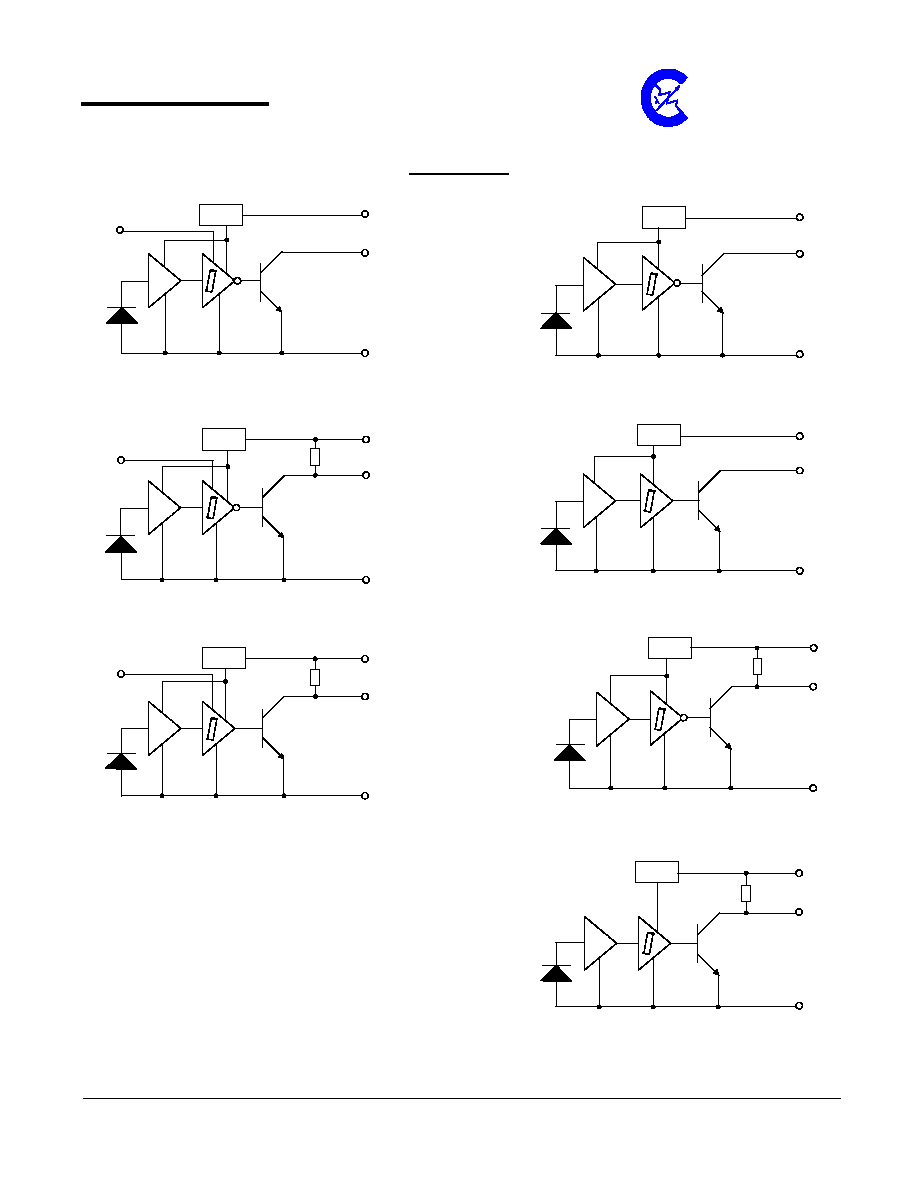
Schematics
Clairex
Technologies, Inc
.
Æ
V
CC
ADJ
V
OUT
GND
CLL133/CLL133W
Open collector ≠ inverter with Adjust
V
CC
ADJ 10k
V
OUT
GND
CLL131/CLL131W
10k pull-up ≠ inverter with Adjust
V
CC
ADJ 10k
V
OUT
GND
CLL130/CLL130W
10k pull-up ≠ buffer with Adjust
V
REG
LA
V
CC
V
OUT
GND
CLL135/CLL135W
Open collector - inverter
V
CC
V
OUT
GND
CLL134/CLL134W
Open collector - buffer
V
REG
LA
V
REG
V
REG
LA
V
REG
LA
V
CC
10k
V
OUT
GND
CLL137/CLL137W
10k pull-up ≠ inverter
V
REG
LA
V
CC
10k
V
OUT
GND
CLL136/CLL136W
10k pull-up ≠ buffer
V
REG
LA
Clairex reserves the right to make changes at any time to improve design and to provide the best possible product. Page 2 of 4
LA
Clairex Technologies, Inc. 1845 Summit Ave., #404 Plano, Texas 75074-8148
Phone: 972-422-4676 Fax: 972-423-8628 www.clairex.com
CLL Series
Photo-IC Sensors
Digital Output
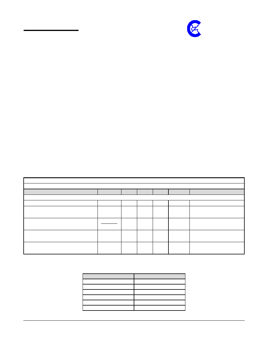
Absolute maximum ratings (T
A
= 25∞C unless otherwise stated)
storage temperature ........................................................................................................ -65∞C to +150∞C
operating
temperature ..................................................................................................... -55∞C to +125∞C
lead soldering temperature
(1)
............................................................................................................240∞C
V
CC
supply voltage...................................................................................................................4.5V to 18V
V
ADJ
(CLL130-CLL133 and CLL130W-CLL133W only) ......................................................................... 3V
V
OUT
(10k pull-up series)
(2)
................................................................................................................ 18V
V
OUT
(open collector series)
(2)
.............................................................................................................. 30V
I
SINK
(3)
................................................................................................................................................ 25mA
Power
dissipation ....................................................................................................................... 250mW
(4)
NOTES:
1. 1/16" from the case for 5 seconds maximum. Maximum temperature can be
260∞C if wave soldering.
2. This rating applies when the output is in the OFF state only.
3. This rating applies when the output is in the ON state only.
4. Derate linearly 2.5mW/∞C from 25∞C free air to T
A
= 125∞C.
5. CLL130-CLL133 and CLL130W-CLL133W photo-IC sensors are tested with the ADJ lead open.
6. Light source is an AlGaAs IRED with peak wavelength at 880nm.
DEFINITIONS:
∑ E
e
(+) is the minimum irradiance required to cause the output to change state.
∑ Buffer: Output is HIGH when input irradiance is >E
e
(+).
∑ Inverter: Output is LOW when input irradiance is >E
e
(+).
electrical characteristics (T
A
= 25∞C unless otherwise noted)
parameter
symbol
min
typ
max
units
test conditions
Operating supply voltage
V
CC
4.5 - 18 V
Positive going threshold
irradiance
(6)
E
e
(+)
0.005
-
0.05 mW/cm
2
4.5V V
CC
18V,
ADJ open
Hysteresis ratio
E
eT
(+)
E
eT
(-)
1.2 - 1.8 operate
point/release
point
Supply current
I
CC
- -
12
mA
4.5V
V
CC
18V, Ee = 0
or 0.5mW, ADJ open
Total acceptance angle
P
-
-
30
70
-
-
deg.
deg.
All non-suffix W parts
All suffix W parts
Gain threshold can be adjusted on the CLL130-CLL133 and CLL130W-CLL133W series by
placing a resistor between the ADJ and GND leads in accordance with the following table.
Decreasing the resistance causes the output to switch at a higher threshold level.
ADJ Resistor
Normalized Threshold
open 1.00
10k 2.00
4.7k 2.75
2.2k 3.75
1k 5.00
Connected to GND
7.25
Clairex
Technologies, Inc
.
Æ
Clairex reserves the right to make changes at any time to improve design and to provide the best possible product. Page 3 of 4
Clairex Technologies, Inc. 1845 Summit Ave., #404 Plano, Texas 75074-8148
Phone: 972-422-4676 Fax: 972-423-8628 www.clairex.com
CLL Series
Photo-IC Sensors
Digital Output
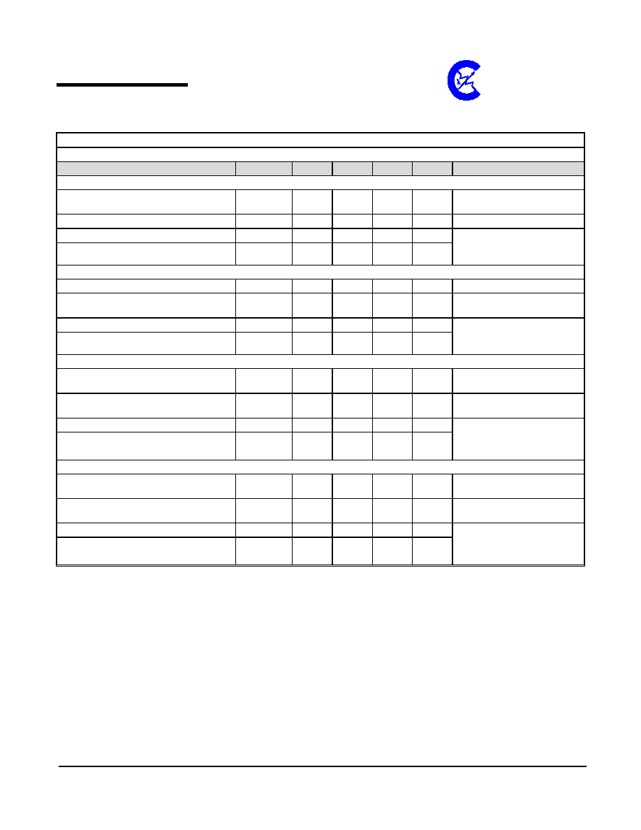
electrical characteristics (T
A
= 25∞C unless otherwise noted)
parameter
symbol
min
typ
max
units
test conditions
CLL130/CLL130W and CLL136/CLL136W (buffer, 10k pull-up)
High state output voltage
V
OH
4.5 - - V
V
CC
= 5.0V,
E
e
(+) 0.5mW/cm
2
Low state output voltage
V
OL
- -
0.4
V
V
CC
= 5.0V, E
e
(+) = 0
Output rise and fall time
t
r
, t
f
-
75
- ns
Propagation delay
t
PHL,
t
PLH
- 5 - µs
V
CC
= 5.0V, E
e
= 0 or
0.5mW/cm
2
, f = 10kHz,
DC = 50%, R
L
= 330
CLL131/CLL131W and CLL137/CLL137W (inverter, 10k pull-up)
High state output voltage
V
OH
4.5 - - V
V
CC
= 5.0V, E
e
(+) = 0
Low state output voltage
V
OL
- -
0.4
V
V
CC
= 5.0V,
E
e
(+) 0.5mW/cm
2
Output rise and fall time
t
r
, t
f
-
75
- ns
Propagation delay
t
PHL,
t
PLH
- 5 - µs
V
CC
= 5.0V, E
e
= 0 or
0.5mW/cm
2
, f = 10kHz,
DC = 50%, R
L
= 330
CLL134/CLL134W (buffer, open collector)
High state output current
I
OH
- -
100
µA
V
CC
= 5.0V, V
OH
= 30V
E
e
(+) 0.5mW/cm
2
Low state output voltage
V
OL
- -
0.4
V
V
CC
= 5.0V, E
e
(+) = 0
R
L
= 330
Output rise and fall time
t
r
, t
f
-
75
- ns
Propagation delay
t
PHL,
t
PLH
- 5 - µs
V
CC
= 5.0V, E
e
= 0 or
0.5mW/cm
2
, f = 10kHz,
DC = 50%, R
L
= 330
CLL133/CLL133W and CLL135/CLL135W (inverter, open collector)
High state output current
I
OH
- -
100
µA
V
CC
= 5.0V, V
OH
= 30V
E
e
(+) = 0
Low state output voltage
V
OL
- -
0.4
V
V
CC
= 5.0V, R
L
= 330
E
e
(+) 0.5mW/cm
2
Output rise and fall time
t
r
, t
f
-
75
- ns
Propagation delay
t
PHL,
t
PLH
- 5 - µs
V
CC
= 5.0V, E
e
= 0 or
0.5mW/cm
2
, f = 10kHz,
DC = 50%, R
L
= 330
NOTE: Due to the high sensitivity of the CLL series, when used in high speed switching
applications, Clairex recommends installing a 0.1µF capacitor between V
CC
and GND.
Clairex reserves the right to make changes at any time to improve design and to provide the best possible product. Page 4 of 4
Clairex
Technologies, Inc
.
Æ