
PRELIMINAR
Y
CPC1017N
Units
Load Voltage
60
V
Load Current
100
mA
Max R
ON
16
Current to operate
1.0
mA
Part #
Description
CPC1017N
4 Pin SOP (100/tube)
CPC1017NTR
4 Pin SOP (2,000/reel)
www.clare.com
DS-CPC1017N-R0A.1
CPC1017N
4 Pin SOP OptoMOS
Æ
Relays
1
Applications
Features
Description
Approvals
Ordering Information
Pin Configuration
Switching Characteristics of
Normally Open (Form A) Devices
CONTROL
LOAD
10ms
10%
10%
90%
+
T
ON
T
OFF
+
+
∑
Design for use in security systems complying with
EN50130-4
∑
Only 1mA of LED curent required to operate
∑
Small 4 Pin SOP Package
∑
TTL/CMOS Compatible input
∑
No Moving Parts
∑
High Reliability
∑
Arc-Free With No Snubbing Circuits
∑
1500V
RMS
Input/Output Isolation/2100V AC peak
∑
No EMI/RFI Generation
∑
Immune to radiated EM fields
∑
SMD Pick & Place, Wave Solderable
∑
Tape & Reel Version Available
∑
Security
∑
Passive Infrared Detectors (PIR)
∑
Data Signalling
∑
Sensor Circuitry
∑
Instrumentation
∑
Multiplexers
∑
Data Acquisition
∑
Electronic Switching
∑
I/O Subsystems
∑
Meters (Watt-Hour, Water, Gas)
∑
Medical Equipment--Patient/Equipment Isolation
∑
Aerospace
∑
Industrial Controls
The CPC1017N is a miniature 1-Form-A solid state
relay in a 4 pin SOP package that employs optically
coupled MOSFET technology to provide 1500V of
input to output isolation. The super efficient MOSFET
switches and photovoltaic die use Clare's patented
OptoMOS architecture. The optically coupled input is
controlled by a highly efficient GaAIAs infrared LED.
The CPC1017N uses Clare's state-of-the-art double
molded vertical construction packaging to produce
the world's smallest relay. The CPC1017N offers
board space savings of at least 20% over the com-
petitor's larger 4 pin SOP relay. It boasts the indus-
tries' lowest input current to operate in its class.
∑
UL Recognized Component
∑
BSI Certified to EN60950
1
2
3
4
+ Control
≠ Control
Load
Load
CPC1017N Pinout

PRELIMINAR
Y
Parameter
Conditions
Symbol
Min
Typ
Max
Units
Output Characteristics @ 25
∞
C
Load Voltage (Peak)
I
L
=1
µA
V
L
-
-
60
V
Load Current (Continuous)
AC Peak
1
I
F
=10mA
I
L
-
-
100
mA
Peak Load Current
10ms
I
LPK
-
-
350
mA
On-Resistance
2
I
L
=100mA
R
ON
-
-
16
Off-State Leakage Current
V
L
=60V
I
LEAK
-
-
1
µA
Switching Speeds
Turn-On
I
F
=5mA, V
L
=10V
T
ON
-
-
10
ms
Turn-Off
I
F
=5mA, V
L
=10V
T
OFF
-
10
ms
Output Capacitance
50V; f=1MHz
C
OUT
-
25
-
pF
Capacitance
Input to Output
-
-
-
1
-
pF
Input Characteristics @ 25
∞
C
Input Control Current
3
I
L
=150mA
I
F
1
-
50
mA
Input Dropout Current
-
I
F
0.3
0.9
-
mA
Input Voltage Drop
I
F
=5mA
V
F
0.9
1.2
1.4
V
Reverse Input Voltage
-
V
R
-
-
5
V
Reverse Input Current
V
R
=5V
I
R
-
-
10
µA
1
Load current derates linearly from 100mA @ 25
o
C to 80mA @ 80
o
C.
2
Measurement taken within 1 second of on time.
3
For applications requiring high temperature operation (greater than 60
o
C) an LED drive current of 3mA is recommended.
www.clare.com
2
CPC1017N
R0A.1
Absolute Maximum Ratings are stress ratings. Stresses in
excess of these ratings can cause permanent damage to
the device. Functional operation of the device at these or
any other conditions beyond those indicated in the opera-
tional sections of this data sheet is not implied. Exposure of
the device to the absolute maximum ratings for an extend-
ed period may degrade the device and effect its reliability.
Absolute Maximum Ratings (@ 25∞ C)
Parameter
Min
Typ
Max Units
Input Power Dissipation
-
-
70
mW
Input Control Current
-
-
50
mA
Peak (10ms)
-
-
1
A
Reverse Input Voltage
-
-
5
V
Total Power Dissipation
-
-
400
1
mW
Isolation Voltage Input
to Output(AC Peak test voltage)
2100
-
-
V
peak
Operational Temperature
-40
-
+85
∞
C
Storage Temperature
-40
-
+125
∞
C
Soldering Temperature
-
-
+220
∞
C
(10 Seconds Max.)
1
Derate Linearly 3.33 mw /
o
C
Electrical Characteristics

CPC1017N
www.clare.com
3
R0A.1
PRELIMINAR
Y
CPC1017N
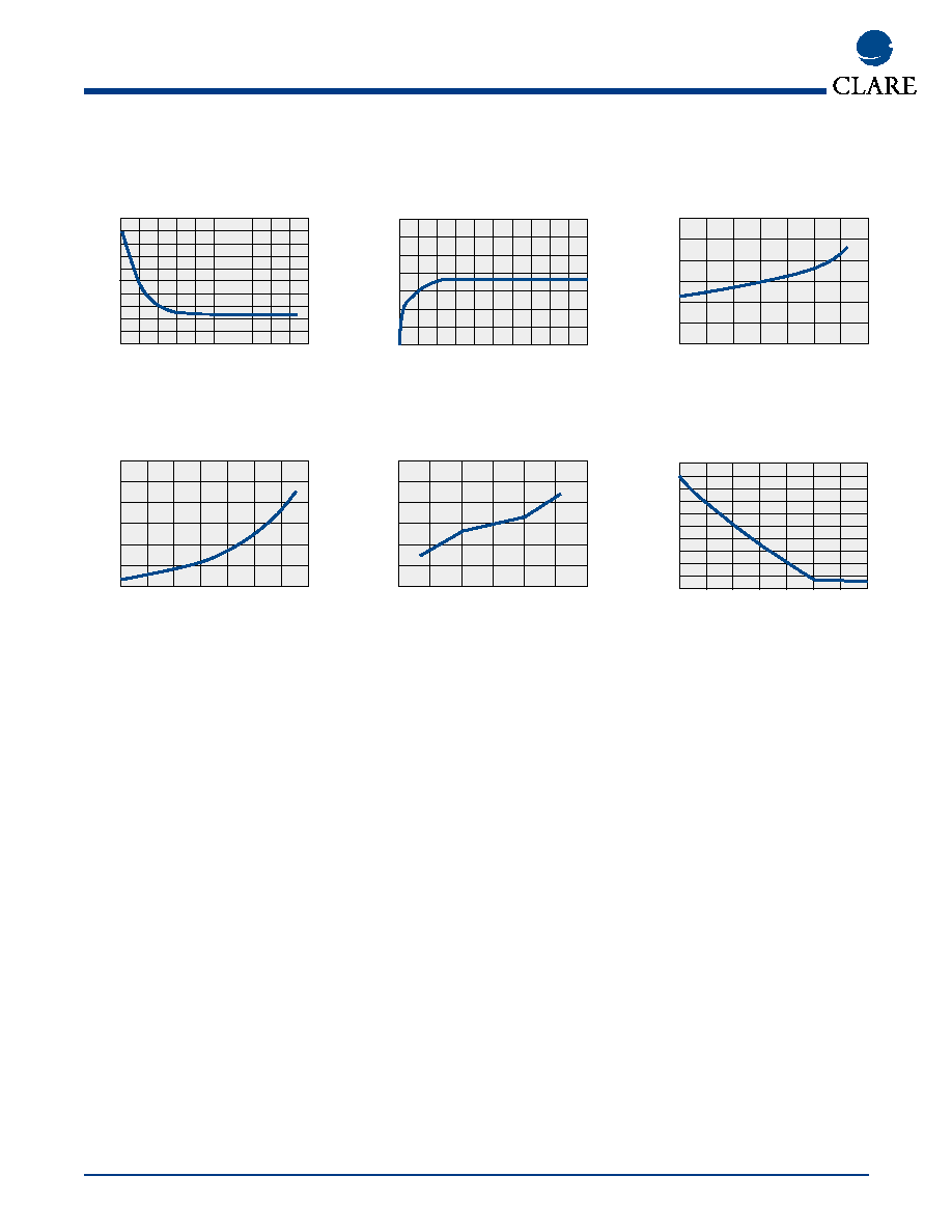
Typical LED Forward Voltage Drop
vs. Temperature
Temperature ( C)
LED Forward Voltage Drop (V)
1.8
1.6
1.4
1.2
1.0
0.8
-40
-20
0
20
40
60
80
120
100
50mA
10mA
5mA
o
CPC1017N
Typical Turn-Off vs. Temperature
(Load Current = 50mA)
Temperature ( C)
Turn-Off (ms)
-40
1.000
0.900
0.800
0.700
0.600
0.500
0.400
0.300
0.200
0.100
0
-20
0
20
40
60
80
100
o
I =5mA
F
I =2mA
F
CPC1017N
Typical Turn-On vs. Temperature
(Load Current = 50mA)
Temperature ( C)
Turn-On (ms)
-40
5.000
4.500
4.000
3.500
3.000
2.500
2.000
1.500
1.000
0.500
0
-20
0
20
40
60
80
100
o
I =5mA
F
I =2mA
F
CPC1017N
Typical Leakage vs. Temperature
(Measured across Pins 3 & 4) I
L
= max rated
Temperature ( C)
Leakage (
µ
A)
-40
0.016
0.014
0.012
0.010
0.008
0.006
0.004
0.002
0
-20
0
20
40
60
80
100
o
CPC1017N
Typical Load Current vs. Temperature
Temperature ( C)
Load Current (mA)
180
160
140
120
100
80
60
40
20
0
-40
-20
0
20
40
60
80
120
100
I =2mA
F
o
I =5mA
F
CPC1017N
Typical Turn-Off Time
(Ambient Temperature = 25 C)
(Load Current = 100mA; I
F
= 5mA)
0.26
0.30
0.34
0.38
0.36
0.32
0.28
Turn-Off (ms)
Device Count (N)
25
20
15
10
5
0
o
CPC1017N
Typical Turn-On Time
(Ambient Temperature = 25 C)
(Load Current = 100mA; I
F
= 5mA)
1.0
1.2
1.4
1.6
1.1
1.3
1.5
Turn-On (ms)
Device Count (N)
25
20
15
10
5
0
o
CPC1017N
Typical I
F
for Switch Dropout
(Ambient Temperature = 25 C)
(Load Current = 100mA)
25
20
15
10
5
0
0.35
0.45
0.55
0.30
0.40
0.50
0.60
LED Current (mA)
Device Count (N)
o
CPC1017N
Typical On-Resistance Distribution
(Ambient Temperature = 25 C)
(Load Current = 100mA)
35
30
25
20
15
10
5
0
On-Resistance (
)
Device Count (N)
o
6.8
6.9
7.1
7.0
7.4
7.2
7.3
CPC1017N
Typical LED Forward Voltage Drop
(Ambient Temperature = 25 C)
I
F
= 5mADC
35
30
25
20
15
10
5
0
1.17
1.19
1.21
1.23
1.25
LED Forward Voltage Drop (V)
Device Count (N)
o
PERFORMANCE DATA*
CPC1017N
Typical I
F
for Switch Operation
(Ambient Temperature = 25 C)
(Load Current = 100mA)
0.35
0.45
0.55
0.30
0.40
0.50
0.60
LED Current (mA)
Device Count (N)
25
20
15
10
5
0
o
CPC1017N
Typical Turn-Off vs. Temperature
(Load Current = 50mA)
Temperature ( C)
Turn-Off (ms)
-40
1.000
0.900
0.800
0.700
0.600
0.500
0.400
0.300
0.200
0.100
0
-20
0
20
40
60
80
100
o
I =5mA
F
I =2mA
F
* The Performance data shown in the graphs above is typical of device performance. For guaranteed parameters not indicated in the written specifications, please contact our application
department.
www.clare.com
4
CPC1017N
R0A.1
PRELIMINAR
Y
CPC1017N
Typical On-Resistance vs. Temperature
(Load Current = 50mA; I
F
= 5mA)
Temperature ( C)
On-Resistance ( )
-40
60
50
40
30
20
10
0
-20
0
20
40
60
80
100
o
CPC1017N
Typical Turn-Off vs. LED Forward Current
(Load Current = 100mA)
LED Forward Current (mA)
Turn-Off (ms)
0
5
10
15
20
25
30
35
40
45
0.7
0.6
0.5
0.4
0.3
0.2
0.1
0
50
CPC1017N
Typical Turn-On vs. LED Forward Current
(Load Current = 100mA; I
F
=5mA)
LED Forward Current (mA)
Turn-On (ms)
0
5
10
15
20
25
30
35
40
45
3.0
2.7
2.4
2.1
1.8
1.5
1.2
0.9
0.6
0.3
0
50
PERFORMANCE DATA*
* The Performance data shown in the graphs above is typical of device performance. For guaranteed parameters not indicated in the written specifications, please contact our application
department.
CPC1017N
Typical I
F
for Switch Operation
vs. Temperature
(Load Current = 50mA)
Temperature ( C)
LED Current (mA)
-40
3.000
2.500
2.000
1.500
1.000
0.500
0
-20
0
20
40
60
80
100
o
CPC1017N
Typical Load Current vs. Load Voltage
(Ambient Temperature = 25 C)
I
F
= 5mA
Load Voltage (V)
Load Current (mA)
150
100
50
0
-50
-100
-150
-3
-2
-1
0
1
2
3
o
CPC1017N
Energy Rating Curve
Time
Load Current (A)
10
µs
1.0
0.9
0.8
0.7
0.6
0.5
0.4
0.3
0.2
0.1
0
1ms
100
µs
100ms
1s
10ms
10s
100s
CPC1017N
www.clare.com
5
R0A.1
PRELIMINAR
Y
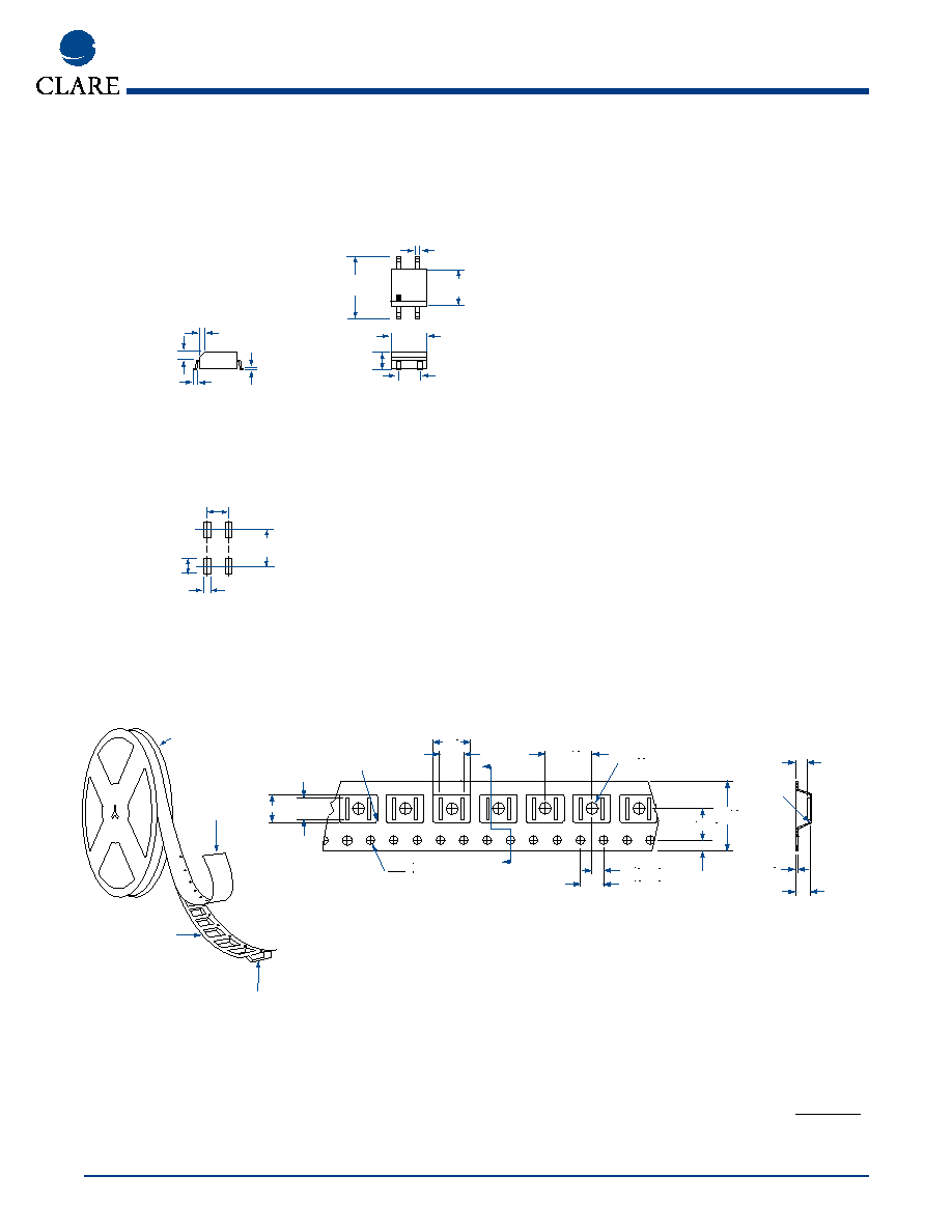
.20 ± .025
(.008 ± .001)
2.54 TYP.
(.100 TYP.)
2.16 MAX.
(.085)
1.02 ± .025
(.040 ± .001)
3.81 ± .08
(.150 ± .003)
6.096 ± .102
(.240 ± .004)
.38 x 45º
(.015 x 45º )
.38 TYP.
(.015 TYP.)
4.09 ± 0.20
(0.161 ± 0.008)
.432 ± .127
(.017 ± .005)
Dimensions
mm
(inches)
MECHANICAL DIMENSIONS
4 Pin SOIC Narrow ("N" Suffix)
PC Board Pattern (Top View)
2.54
± 0.127
(0.100
± 0.005)
5.66
± 0.14
(0.223
± 0.005)
1.448
(0.057)
0.889
(0.035)
4.70 0.15
3.0 R
1.50
1.60
A
A
8.00
2.00 .05
+
_
4.00 .10
+
_
1.5 dia
5.50 .10
+
_
12.00
1.75
.30
.3 R MAX
TYP
2.30 0.15
SECTION A-A
Tape and Reel Packaging for 4 pin SOIC package
330.2 DiA
(13.00")
Top Cover
Tape Thickness
0.102 MAX
(0.004)
3.8
TYP
+
_
4.2
+
_
2.7 0.15
+
_
Embossment
Embossed
Carrier
6.50
0.15
+
_