 | –≠–ª–µ–∫—Ç—Ä–æ–Ω–Ω—ã–π –∫–æ–º–ø–æ–Ω–µ–Ω—Ç: CPC1906Y | –°–∫–∞—á–∞—Ç—å:  PDF PDF  ZIP ZIP |
www.clare.com
DS-CPC1906Y-R03
1
CPC1906Y
Power SIP Relay
Part #
Description
CPC1906Y
Power SIP Package (25 per tube)
CPC1906Y
Units
Blocking Voltage
60
V
Load Current
2
A
rms
On-Resistance
0.3
Applications
Features
Description
Ordering Information
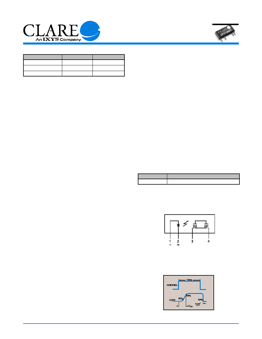
Pin Configuration
∑
Industrial Controls
∑
Motor Control
∑
Robotics
∑
Medical Equipment--Patient/Equipment Isolation
∑
Instrumentation
∑
Multiplexers
∑
Data Acquisition
∑
Electronic Switching
∑
I/O Subsystems
∑
Meters (Watt-Hour, Water, Gas)
∑
IC Equipment
∑
Home Appliances
∑
Power SIP Package
∑
Handle Load Currents Up to 2A
rms
∑
High Reliability
∑
No Moving Parts
∑
Low Drive Power Requirements (TTL/CMOS
Compatible)
∑
Arc-Free With No Snubbing Circuits
∑
2500V
rms
Input/Output Isolation
∑
No EMI/RFI Generation
∑
Machine Insertable, Wave Solderable
Clare and IXYS have combined to bring OptoMOS
Æ
technology, reliability and compact size to a new
family of high power solid state relays. As part of
that family, the CPC1906Y is a 1-Form-A solid state
relay. The CPC1906Y employs optically coupled
MOSFET technology to provide 2500V
rms
of input
to output isolation. The efficient MOSFET switches
and photovoltaic die use Clare's patented OptoMOS
architecture while the input is controlled by a highly
efficient GaAlAs infrared LED. The combination of
low on resistance and high load current handling
capabilities makes the relay suitable for a variety of
high performance switching applications.
CPC1906Y Pinout
Switching Characteristics of Normally
Open (Form A) Devices
Approvals
∑
UL recognized component: File # E69938
∑
Certified to: UL 508
www.clare.com
2
CPC1906Y
R03
Absolute Maximum Ratings are stress ratings. Stresses in
excess of these ratings can cause permanent damage to
the device. Functional operation of the device at conditions
beyond those indicated in the operational sections of this
data sheet is not implied.
Absolute Maximum Ratings (@ 25∞ C)
Parameter
Ratings
Units
Blocking Voltage
60
V
Reverse Input Voltage
5
V
Input control Current
50
mA
Peak (10ms)
1
A
Input Power Dissipation
1
150
mW
Isolation voltage Input to Output
2500
V
rms
Operational Temperature
-40 to +85
∞C
Storage Temperature
-40 to +125
∞C
1
Derate Linearly 3.33 mw / ∫C
Parameter
Conditions
Symbol
Min
Typ
Max
Units
Output Characteristics @ 25∞C
Load Current, Continuous
free air
I
L
-
-
2
A
rms
Peak Load Current
T=10ms
I
LPK
-
-
9
A
rms
On-Resistance
1
I
L
=1A
R
ON
-
0.105
0.3
Off-State Leakage Current
V
L
=60V
I
LEAK
-
-
1
µA
Switching Speeds
Turn-On
I
F
=10mA, V
L
=10V
T
ON
-
3.5
10
ms
Turn-Off
I
F
=10mA, V
L
=10V
T
OFF
-
0.04
5
ms
Output Capacitance
50V, f=1MHz
C
OUT
-
130
-
pF
Input Characteristics @ 25∞C
Input Control Current
I
L
=1A
I
F
10
-
-
mA
Input Dropout Current
-
I
F
0.6
-
-
mA
Input Voltage Drop
I
F
=5mA
V
F
0.9
1.2
1.4
V
Reverse Input Current
V
R
=5V
I
R
-
-
10
µA
Input/Output Characteristics @ 25∞C
Capacitance Input/Output
f=1MHz
I
I/O
I/O
-
2
-
pF
1
Measurement taken within 1 second of on time.
Electrical Characteristics
Parameter
Conditions
Symbol
Min
Typ
Max
Units
Thermal Resistance (junction to case)
-
R
JC
-
1.5
-
∞C/W
Thermal Characteristics
CPC1906Y
www.clare.com
3
R03
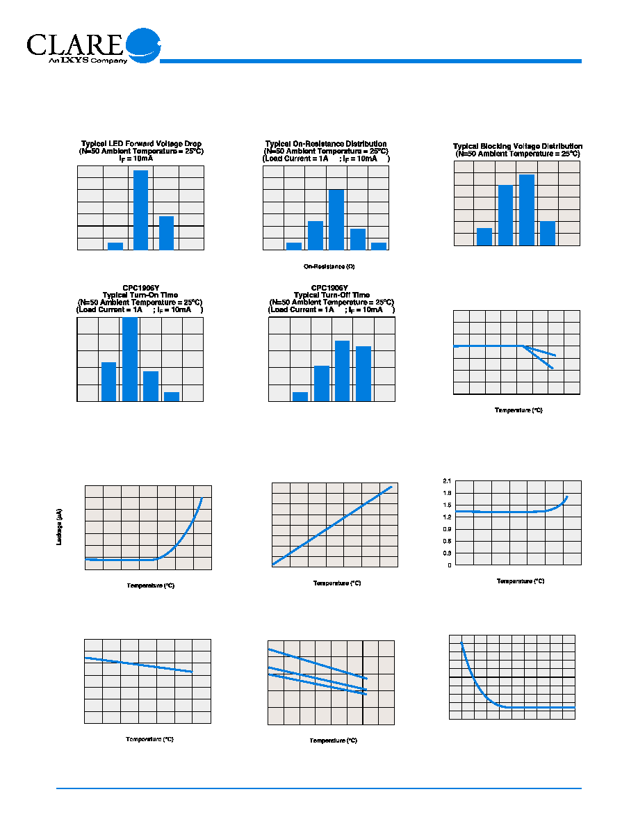
PERFORMANCE DATA*
*The Performance data shown in the graphs above is typical of device performance. For guaranteed parameters not indicated in the written specifi cations, please contact our
application department.
35
30
25
20
15
10
5
0
1.17
1.19
1.21
1.23
1.25
LED Forward Voltage (V)
Device Count (N)
CPC1906Y
DC
35
30
25
20
15
10
5
0
0.103 0.104 0.105
0.107
0.106
0.108
Device Count (N)
CPC1906Y
DC
DC
35
30
25
20
15
10
5
0
66
68
70
67
69
71
Blocking Voltage (V)
Device Count (N)
CPC1906Y
3.0
4.0
5.0
2.5
3.5
4.5
Turn-On (ms)
Device Count (N)
25
20
15
10
5
0
DC
DC
0.033
0.042
0.050
0.033
0.037
0.046
Turn-Off (ms)
Device Count (N)
25
20
15
10
5
0
DC
DC
CPC1906Y
Typical Load Current vs. Temperature
Load Current (A
rm
s
)
3.5
3.0
2.5
2.0
1.5
1.0
0.5
0.0
-40
-20
0
20
40
60
80
120
100
I
F
= 5mA
I
F
= 10mA
CPC1906Y
Typical Leakage vs. Temperature at
Maximum Rated Voltage
(Measured across Pins 3 & 4)
-40
0.035
0.030
0.025
0.020
0.015
0.010
0.005
0
-20
0
20
40
60
80
100
CPC1906Y
Blocking Voltage vs. Temperature
Blocking Voltage (V)
-40
-20
0
20
40
60
80
100
72
71
70
69
68
67
66
65
64
Turn-On (ms)
-40
-20
0
20
40
60
80
100
I
F
= 10mA
CPC1906Y
Typical Turn-On vs. Temperature
(Load Current = 100 mA
DC
)
Turn-Off (ms)
-40
0.70
0.60
0.50
0.40
0.30
0.20
0.10
0
-20
0
20
40
60
80
100
I
F
= 10mA
CPC1906Y
Typical Turn-Off vs. Temperature
(Load Current = 100 mA
DC
)
CPC1906Y
Typical LED Forward Voltage Drop
vs. Temperature
LED Forward Voltage Drop (V)
I
F
= 50mA
I
F
= 10mA
I
F
= 20mA
1.8
1.6
1.4
1.2
1.0
0.8
-40
-20
0
20
40
60
80
120
100
CPC1906Y
Typical Turn-On vs.LED Forward Current
(Load Current = 100 mA
DC
)
LED Forward Current (mA)
Turn-On (ms)
0
5
10 15 20 25 30 35 40 45 50
4.0
3.6
3.2
2.8
2.4
2.0
1.6
1.2
0.8
0.4
0

www.clare.com
4
CPC1906Y
R03
PERFORMANCE DATA*
*The Performance data shown in the graphs above is typical of device performance. For guaranteed parameters not indicated in the written specifi cations, please contact our
application department.
CPC1906Y
Typical Turn-Off vs. LED Forward Current
(Load Current = 100 mA
DC
)
LED Forward Current (mA)
Turn-Off (ms)
0
5
10 15 20 25 30 35 40 45 50
0.09
0.08
0.07
0.06
0.05
0.04
0.03
0.02
0.01
0
CPC1906Y
Typical On-Resistance vs. Temperature
(Load Current = 100 mA
DC
)
-40
-20
0
20
40
60
80
100
I
F
= 10mA
I
F
= 5mA
CPC1906Y
Typical I
F
for Switch Operation
vs. Temperature
(Load Current = 100 mA
DC
)
LED Current (mA)
-40
10.0
9.0
8.0
7.0
6.0
5.0
4.0
3.0
2.0
1.0
0
-20
0
20
40
60
80
100
Load Voltage (V)
Load Current (A)
-0.4
-0.267 -0.133
0.133 0.267
0
0.4
3.75
3.00
2.25
1.50
0.75
0.00
-0.75
-1.50
-2.25
-3.00
-3.75
CPC1906Y
DC
CPC1906Y
Energy Rating Curve
(Free air, no heat sink)
Time
Load Current (A
rm
s
)
16
14
12
10
8
6
4
2
0
1ms
100ms
10s
10ms
1s
100s
Clare, Inc. makes no representations or warranties with respect to the accuracy or completeness of the contents of this publication and reserves the right to make changes to specifications and product
descriptions at any time without notice. Neither circuit patent licenses nor indemnity are expressed or implied. Except as set forth in Clare's Standard Terms and Conditions of Sale, Clare, Inc. assumes no
liability whatsoever, and disclaims any express or implied warranty, relating to its products including, but not limited to, the implied warranty of merchantability, fitness for a particular purpose, or infringement
of any intellectual property right.
The products described in this document are not designed, intended, authorized or warranted for use as components in systems intended for surgical implant into the body, or in other applications intended
to support or sustain life, or where malfunction of Clare's product may result in direct physical harm, injury, or death to a person or severe property or environmental damage. Clare, Inc. reserves the right to
discontinue or make changes to its products at any time without notice.
Specification: DS-CPC1906Y-R03
©Copyright 2005, Clare, Inc.
OptoMOS
Æ
is a registered trademark of Clare, Inc.
Æ
Æ
All rights reserved. Printed in USA.
5/26/05
For additional information please visit our website at: www.clare.com
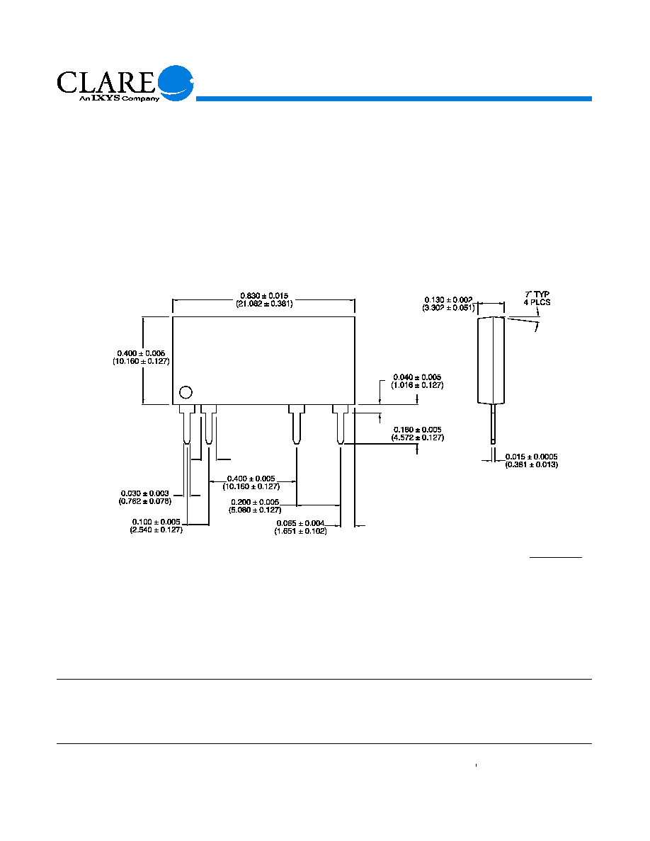
MECHANICAL DIMENSIONS
Dimensions:
inches
(mm)
PIN 1
0.070
(1.778)
PIN 4
Manufacturing Information
Soldering
Recommended soldering processes are limited to
245∫C component body temperature for 10 seconds.
Washing
Clare does not recommend ultrasonic cleaning or the
use of chlorinated solvents.