1
www.clare.com
CPC5604
ANDS-CPC5604-XXX
The CPC5604 is a single package optical Data Access
Arrangement (DAA) device in a low profile surface
mount PCMCIA compatible package. With a few exter-
nal components, the CPC5604 provides a full featured
International 56K capable solution. This device is well
suited for all 56K modems, voice mail systems, fax
machines, computer telephony applications, remote
data access, medical, and security systems. For
International compliance, external passive component
values can be changed or, the CPC5604 can be used
in conjunction with the CPC5601 Programmable Driver
for a host programmable International DAA.
∑
56K Modems/Fax including PCMCIA
∑
Computer Telephony
∑
Voice Mail Systems
∑
Security/alarm systems
∑
Utility Meters
∑
Vending machines
∑
Voice Over IP
∑
Network routers
∑
PBX systems
∑
Home Medical Devices
∑
Plant monitoring equipment
∑
PC Mother Boards
∑
Set Top Boxes (Cable TV Modems)
∑
UL1950/UL1459
∑
EN60950
∑
56K Compatible
∑
Transformerless Optical Design
∑
Complete Ring Detector Circuit
∑
Caller ID Signal Detection
∑
Snoop Circuitry
∑
Integrated Hybrid
∑
Small 32-Pin Plastic Package
∑
PCMCIA Compatible
∑
PCB Space and Cost Savings
∑
compatible with all modem speeds including V.90
∑
FCC compliant
∑
Compatible with U.S. and International dial up
Phone lines
∑
CTR-21 Compliant
Applications
Features
Description
Approvals
Optical Data Access Arrangement I.C.
Ordering Information
Part #
Description
CPC5604A
Data Access Arrangement,
Tape and Reel
CPC5604ATR
Data Access Arrangement,
Tape and Reel
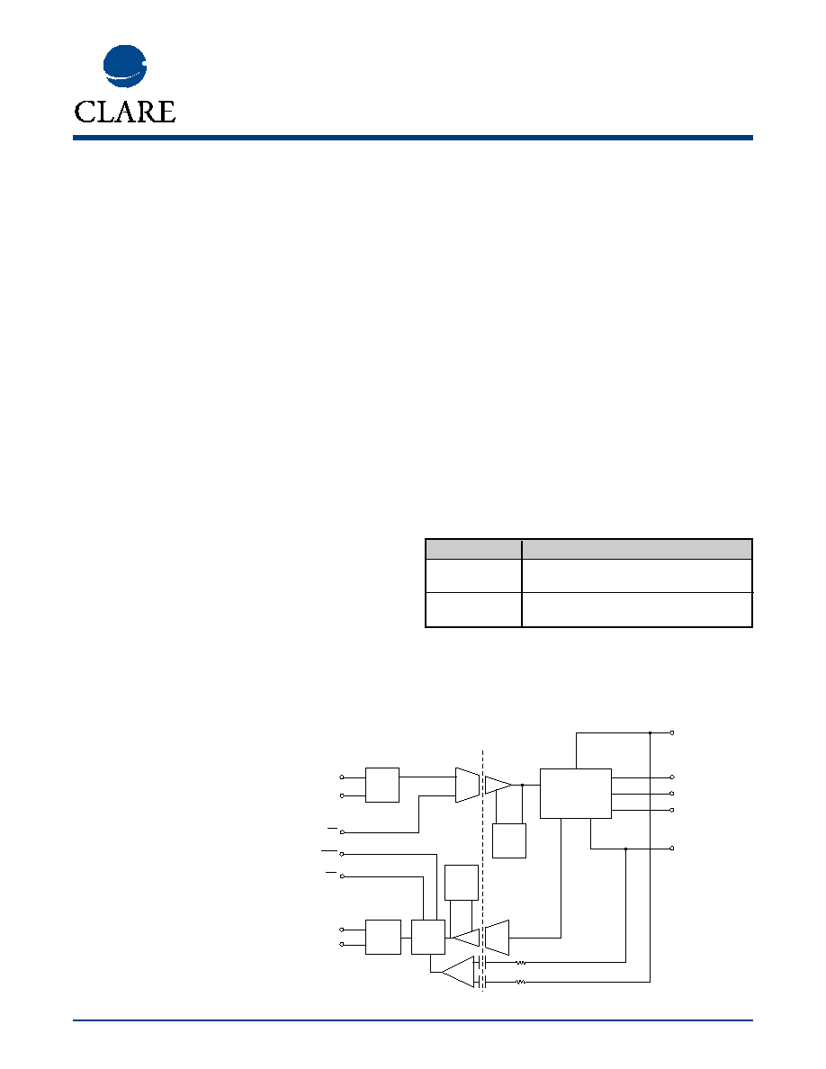
Block Diagram
Transconductance
Stage
2-4 Wire Hybrid
AC/DC Termination
Hookswitch
Isolation Barrier
Vref
AGC
Vref
AGC
Snoop Amplifier
Receive
Isolation
Amplifier
Transmit
Isolation
Amplifier
TIP+
RING-
Transmit
Diff.
Amplifier
Receive
Diff.
Amplifier
CID/
RING
MUX
Tx+
Tx-
OH
RING
CID
Rx+
Rx-
Current Limit Control
AC Impedance Control
VI Slope Control
C
S
C
S
R
SNOOP
R
SNOOP

www.clare.com
2
CPC5604
XXX
Table of Contents
Table 1 - Performance Specifications ........................................................................................................................3
Table 1 - Performance Specifications (Continued) ....................................................................................................4
Table 2 - Package Pinout ..........................................................................................................................................5
Applications ................................................................................................................................................................6
North American Reference Design Schematic ....................................................................................................6
Table 3 - North American Reference Design Bill of Materials....................................................................................7
International Reference Design Schematic................................................................................................................8
Table 4 - International Reference Design Bill of Materials ........................................................................................9
CTR-21 Reference Design Schematic ....................................................................................................................10
Table 5 - Reference Design Schematic Bill of Materials ..........................................................................................11
CTR-21 with Exceptions Reference Design Schematic ..........................................................................................12
Table 6 - CTR-21 with Exceptions Reference Design Bill of Materials ..................................................................13
Introduction ..............................................................................................................................................................14
Ring Detection via Snoop Circuit ........................................................................................................................14
Caller ID (CID) Detection via Snoop Circuit ......................................................................................................14
Hook Switch Control ..........................................................................................................................................14
Transmit Signal ..................................................................................................................................................14
Receive Signal Path ................................................................................................................................................15
Transmit Signal Path ................................................................................................................................................15
Ring Signal Detection ..............................................................................................................................................16
Figure 3 - Caller ID Protocol ....................................................................................................................................17
DC Charcteristics......................................................................................................................................................17
Figure 4 - Outlook DC Resistance Tip/Ring Setup ..................................................................................................18
On-Hook Resistance ................................................................................................................................................18
Current Limiting ........................................................................................................................................................18
CTR-21 Compliance ................................................................................................................................................18
AC Characteristics ....................................................................................................................................................18
Differential and Single Ended Mode ........................................................................................................................19
Receive and Transmit Frequency Response ..........................................................................................................19
Figure 4C - Transmit Frequency Response Setup ..................................................................................................20
Figure 4D - Transmit Frequency Response Tx±......................................................................................................20
Distortion ..................................................................................................................................................................21
Figure 5C - Transmit Distortion Text Tx± to Tip/Ring Setup ....................................................................................22
Figure 5D - Transmit Distortion on Tip/Ring ............................................................................................................22
Trans-Hybrid Loss ....................................................................................................................................................23

CPC5604
www.clare.com
3
XXX
Table of Contents (Continued)
Return Loss ..............................................................................................................................................................24
Snoop Mode Frequency Response..........................................................................................................................25
Snoop Mode Distortion ............................................................................................................................................26
Snoop Mode Common Mode Rejection Ratio (CMRR) ..........................................................................................27
Country Specific Component Values........................................................................................................................28
Interconnection to Rockwell 56K Chipset ................................................................................................................29
Interconnection to Lucent 56K Chipset ....................................................................................................................30
Mechanical Dimensions............................................................................................................................................31

www.clare.com
CPC5604
XXX
Electrical Characteristics
Absolute Maximum Ratings are stress ratings. Stresses
in excess of these ratings can cause permanent damage
to the device. Functional operation of the device at these
or any other conditions beyond those indicated in the
operational sections of this data sheet is not implied.
Exposure of the device to the absolute maximum ratings
for an extended period may degrade the device and effect
its reliability.
4
PARAMETER
MIN
TYP
MAX
UNIT
CONDITION
DC Characteristics
Operating Voltage V
CC
4.75
5
5.25
V
Modem Side
Operating Current I
CC
-
-
15
mA
Modem Side
Operating Voltage V
DD
3.5
-
5.25
V
From Tip and Ring
Operating Current I
DD
-
-
5
mA
Drawn from Tip and Ring
On-Hook Characteristics
DC Resistance (metallic)
10
-
-
M
Tip to Ring, 100VDC Applied
DC Resistance (longitudinal)
10
-
-
M
150VDC Applied from Tip and Ring
to Earth GND
Ring Signal Detection at 68 Hz*
5
-
-
V
Ring Signal Applied to Tip and Ring
Ring Signal Detection at 15 Hz*
28
-
-
V
Ring Signal Applied to Tip and Ring
Snoop Circuit Frequency Response*
600
-
4000
Hz
3dB Corner Frequency
Snoop Circuit CMRR
-
-40
-
dB
120V
RMS
60Hz Common
Mode Signal on Tip/Ring
Ringer Equivalence
-
0.1B
-
REN
-
Longitudinal Balance
60
-
-
dB
Per FCC Part 68.3
Off-Hook Characteristics
AC Impedance*
-
600
-
Tip to Ring
Longitudinal Balance
40
-
-
dB
Tip and Ring to Ground, per FCC part
68.3
Return Loss
-
26
-
dB
Against 600
, 1800Hz

CPC5604
www.clare.com
XXX
3
Table 1 -Performance Specifications (continued)
PARAMETER
MIN
TYP
MAX
UNIT
CONDITION
Transmit/Receive Characteristics
Frequency Response*
30
-
4000
Hz
3dB corner frequency
Trans-Hybrid Loss*
-
30
-
dB
Against 600
resistive, 1800Hz
Transmit Insertion Loss*
-1
0
1
dB
-
Receive Insertion Loss*
-1
0
1
dB
-
Average In-band Noise
-
-100
-
dB
4kHz Flat bandwidth
Harmonic Distortion
-
-
-80
dB
-3dBm, 600Hz, 2nd Harmonic
Transmit Level*
-
-
0
dBm
Single Tone Sine Wave
Receive Level*
-
-
0
dBm
Single Tone Sine Wave
Rx+/Rx- Output Drive Current
-
-
0.5
mA
Sink and Source
Tx+/Tx- Input Impedance
60
90
120
k
-
Isolation Characteristics
Isolation Surge Voltage
1500
-
-
V
SURGE
Line Side to Modem Side
Surge Rise Time
2000
-
-
V/µs
No Damage via T/R
Control Logic (OH, CID, RING)
Input Threshold Voltage
0.8
-
2.0
V
High Level Input Current
-
-
-20
µA
Low Level Input Current
-100
-
-
µA
Output High Voltage
V
CC
-0.4
-
-
V
1M
to Ground
Output Low Voltage
-
-
0.4
V
1M
to VCC
Isolation Voltage
--
-
1500
V
RMS
Tip/Ring Current (continuous)
10
-
120
mA
Total Package Dissipation
--
-
1
W
Operational Temperature
-20
-
+85
∞C
Storage Temperature
-40
-
+125
∞C
Soldering Temperature
(10 seconds Max)
--
-
+220
∞C
Unless Otherwise Noted all Specifications @ 25oC.
* Refer to Typical Application Circuit.