 | –≠–ª–µ–∫—Ç—Ä–æ–Ω–Ω—ã–π –∫–æ–º–ø–æ–Ω–µ–Ω—Ç: CPC7582xC | –°–∫–∞—á–∞—Ç—å:  PDF PDF  ZIP ZIP |
DS-CPC7582-R3.0 10/4/2002
www.clare.com
1
Features
∑
Small 16-pin SOIC or micro-leadframe package
∑
MLP package printed-circuit board footprint is 60
percent smaller than the SOIC version, 70 percent
smaller than 4
th
generation EMR solutions.
∑
Monolithic IC reliability
∑
Low matched R
ON
∑
Eliminates the need for zero cross switching
∑
Flexible switch timing to transition from ringing mode
to talk mode.
∑
Clean, bounce-free switching
∑
Tertiary protection consisting of integrated current
limiting, voltage clamping, and thermal shutdown for
SLIC protection
∑
5 V operation with power consumption < 10 mW
∑
Intelligent battery monitor
∑
Latched logic-level inputs, no external drive circuitry
required
∑
SOIC version is pin compatible with Agere product
Applications
∑
Central office (CO)
∑
Digital Loop Carrier (DLC)
∑
PBX Systems
∑
Digitally Added Main Line (DAML)
∑
Hybrid Fiber Coax (HFC)
∑
Fiber in the Loop (FITL)
∑
Pair Gain System
∑
Channel Banks
Description
The CPC7582 is a monolithic solid-state switch in a
16-pin SOIC or MLP surface-mount package. It
provides the necessary functions to replace two
2-Form-C electro-mechanical relays on traditional
analog and integrated voice and data (IVD) line cards
found in Central Office, Access, and PBX equipment.
The device contains solid state switches for tip and
ring line break, ringing injection/ringing return and test
access. The CPC7582 requires only a +5V supply and
offers break-before-make or make-before-break
switch operation using simple logic-level input control.
The CPC7582xC logic states differ from the
CPC7582xA/B. See "Functional Description" on
page 9 for more information. The CPC7582xC also
has a higher trigger and hold current for the protection
SCR. Specify CPC7582Bx for SOIC or specify
CPC7582Mx for MLP package shipped in tubes. Add
-TR to the part number for tape and reel packaging.
Ordering Information
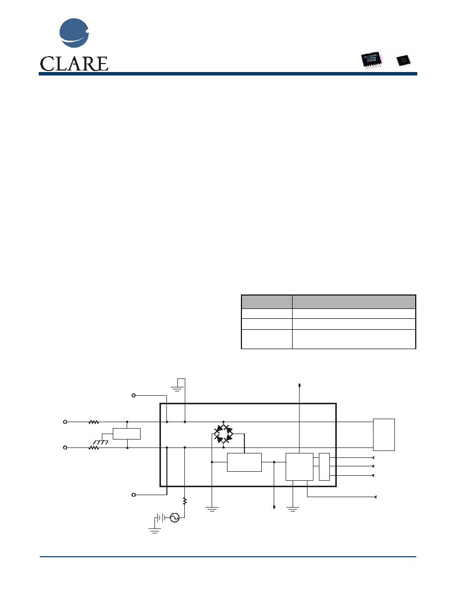
Figure 1. CPC7582 Block Diagram
Part Number
Description
CPC7582xA
6-pole LCAS with protection SCR
CPC7582xB
6-pole LCAS without protection SCR
CPC7582xC
6-pole LCAS with protection SCR and added
logic state
CPC7582
T
LINE
R
LINE
T
BAT
V
DD
R
BAT
D
GND
V
BAT
F
GND
V
REF
IN
ACCESS
IN
RINGING
T
SD
LATCH
3
5
4
14
2
6
7
8
16
1
13
12
15
9
10
11
L
A
T
C
H
Switch
Control
Logic
SCR and
Trip Circuit
(CPC7582xB/C)
Secondary
Protection
+5 Vdc
Tip
Ring
SLIC
X
X
X
X
X
X
SW5
SW6
SW2
SW4
T
TEST
V
BAT
RINGING
300
(min.)
R
TEST
T
RING
SW3
SW1
CPC7582
Line Card Access Switch

CPC7582
2
www.clare.com
R3.0 10/4/2002
1 Specifications . . . . . . . . . . . . . . . . . . . . . . . . . . . . . . . . . . . . . . . . . . . . . . . . . . . . . . . . . . . . . . . . . . . . . . . . . . . . . . . . . . . . . . . . . . . . . . . 3
1.1 Package Pinout . . . . . . . . . . . . . . . . . . . . . . . . . . . . . . . . . . . . . . . . . . . . . . . . . . . . . . . . . . . . . . . . . . . . . . . . . . . . . . . . . . . . . . . . . 3
1.2 Pinout. . . . . . . . . . . . . . . . . . . . . . . . . . . . . . . . . . . . . . . . . . . . . . . . . . . . . . . . . . . . . . . . . . . . . . . . . . . . . . . . . . . . . . . . . . . . . . . . . 3
1.3 Absolute Maximum Ratings (at 25∞ C). . . . . . . . . . . . . . . . . . . . . . . . . . . . . . . . . . . . . . . . . . . . . . . . . . . . . . . . . . . . . . . . . . . . . . . . 4
1.4 Electrical Characteristics, TA = -40∞ C to +85∞ C . . . . . . . . . . . . . . . . . . . . . . . . . . . . . . . . . . . . . . . . . . . . . . . . . . . . . . . . . . . . . . . 4
1.4.1 Power Supply Specifications. . . . . . . . . . . . . . . . . . . . . . . . . . . . . . . . . . . . . . . . . . . . . . . . . . . . . . . . . . . . . . . . . . . . . . . . . . 4
1.4.2 Break Switches, SW1 and SW2 . . . . . . . . . . . . . . . . . . . . . . . . . . . . . . . . . . . . . . . . . . . . . . . . . . . . . . . . . . . . . . . . . . . . . . . 4
1.4.3 Ringing Return Switch, SW3. . . . . . . . . . . . . . . . . . . . . . . . . . . . . . . . . . . . . . . . . . . . . . . . . . . . . . . . . . . . . . . . . . . . . . . . . . 5
1.4.4 Ringing Switch, SW4 . . . . . . . . . . . . . . . . . . . . . . . . . . . . . . . . . . . . . . . . . . . . . . . . . . . . . . . . . . . . . . . . . . . . . . . . . . . . . . . 6
1.4.5 Test Switches, SW5 and SW6 . . . . . . . . . . . . . . . . . . . . . . . . . . . . . . . . . . . . . . . . . . . . . . . . . . . . . . . . . . . . . . . . . . . . . . . . 6
1.5 Additional Electrical Characteristics. . . . . . . . . . . . . . . . . . . . . . . . . . . . . . . . . . . . . . . . . . . . . . . . . . . . . . . . . . . . . . . . . . . . . . . . . . 7
1.6 Protection Circuitry Electrical Specifications . . . . . . . . . . . . . . . . . . . . . . . . . . . . . . . . . . . . . . . . . . . . . . . . . . . . . . . . . . . . . . . . . . . 8
1.7 CPC7582xA/B Truth Table . . . . . . . . . . . . . . . . . . . . . . . . . . . . . . . . . . . . . . . . . . . . . . . . . . . . . . . . . . . . . . . . . . . . . . . . . . . . . . . . 8
1.8 CPC7582xC Truth Table . . . . . . . . . . . . . . . . . . . . . . . . . . . . . . . . . . . . . . . . . . . . . . . . . . . . . . . . . . . . . . . . . . . . . . . . . . . . . . . . . . 9
2 Functional Description. . . . . . . . . . . . . . . . . . . . . . . . . . . . . . . . . . . . . . . . . . . . . . . . . . . . . . . . . . . . . . . . . . . . . . . . . . . . . . . . . . . . . . . . 9
2.1 Introduction . . . . . . . . . . . . . . . . . . . . . . . . . . . . . . . . . . . . . . . . . . . . . . . . . . . . . . . . . . . . . . . . . . . . . . . . . . . . . . . . . . . . . . . . . . . . 9
2.1.1 CPC7582xA/B Logic States . . . . . . . . . . . . . . . . . . . . . . . . . . . . . . . . . . . . . . . . . . . . . . . . . . . . . . . . . . . . . . . . . . . . . . . . . . 9
2.1.2 CPC7582xC Logic States: . . . . . . . . . . . . . . . . . . . . . . . . . . . . . . . . . . . . . . . . . . . . . . . . . . . . . . . . . . . . . . . . . . . . . . . . . . . 9
2.2 Switch Logic. . . . . . . . . . . . . . . . . . . . . . . . . . . . . . . . . . . . . . . . . . . . . . . . . . . . . . . . . . . . . . . . . . . . . . . . . . . . . . . . . . . . . . . . . . . 10
2.2.1 Make-Before-Break Operation - All Versions . . . . . . . . . . . . . . . . . . . . . . . . . . . . . . . . . . . . . . . . . . . . . . . . . . . . . . . . . . . . 10
2.2.2 Make-Before-Break Operation for All Versions (Ringing to Talk Transition). . . . . . . . . . . . . . . . . . . . . . . . . . . . . . . . . . . . . 10
2.2.3 Break-Before-Make Operation - CPC7582xA/B . . . . . . . . . . . . . . . . . . . . . . . . . . . . . . . . . . . . . . . . . . . . . . . . . . . . . . . . . . 10
2.2.4 Break-Before-Make Operation CPC7582xA/B (Ringing to Talk Transition) . . . . . . . . . . . . . . . . . . . . . . . . . . . . . . . . . . . . . 11
2.2.5 Break-Before-Make Operation - All Versions . . . . . . . . . . . . . . . . . . . . . . . . . . . . . . . . . . . . . . . . . . . . . . . . . . . . . . . . . . . . 11
2.2.6 Break-Before-Make Operation for all Version (Ringing to Talk Transition). . . . . . . . . . . . . . . . . . . . . . . . . . . . . . . . . . . . . . 11
2.3 Data Latch . . . . . . . . . . . . . . . . . . . . . . . . . . . . . . . . . . . . . . . . . . . . . . . . . . . . . . . . . . . . . . . . . . . . . . . . . . . . . . . . . . . . . . . . . . . . 12
2.4 TSD . . . . . . . . . . . . . . . . . . . . . . . . . . . . . . . . . . . . . . . . . . . . . . . . . . . . . . . . . . . . . . . . . . . . . . . . . . . . . . . . . . . . . . . . . . . . . . . . . 12
2.5 Ringing Switch Zero-Cross Current Turn Off . . . . . . . . . . . . . . . . . . . . . . . . . . . . . . . . . . . . . . . . . . . . . . . . . . . . . . . . . . . . . . . . . . 12
2.6 Power Supplies . . . . . . . . . . . . . . . . . . . . . . . . . . . . . . . . . . . . . . . . . . . . . . . . . . . . . . . . . . . . . . . . . . . . . . . . . . . . . . . . . . . . . . . . 12
2.7 Battery Voltage Monitor . . . . . . . . . . . . . . . . . . . . . . . . . . . . . . . . . . . . . . . . . . . . . . . . . . . . . . . . . . . . . . . . . . . . . . . . . . . . . . . . . . 12
2.8 Protection. . . . . . . . . . . . . . . . . . . . . . . . . . . . . . . . . . . . . . . . . . . . . . . . . . . . . . . . . . . . . . . . . . . . . . . . . . . . . . . . . . . . . . . . . . . . . 12
2.8.1 Diode Bridge/SCR. . . . . . . . . . . . . . . . . . . . . . . . . . . . . . . . . . . . . . . . . . . . . . . . . . . . . . . . . . . . . . . . . . . . . . . . . . . . . . . . . 12
2.8.2 Current Limiting function . . . . . . . . . . . . . . . . . . . . . . . . . . . . . . . . . . . . . . . . . . . . . . . . . . . . . . . . . . . . . . . . . . . . . . . . . . . . 13
2.9 Temperature Shutdown . . . . . . . . . . . . . . . . . . . . . . . . . . . . . . . . . . . . . . . . . . . . . . . . . . . . . . . . . . . . . . . . . . . . . . . . . . . . . . . . . . 13
2.10 External Protection Elements. . . . . . . . . . . . . . . . . . . . . . . . . . . . . . . . . . . . . . . . . . . . . . . . . . . . . . . . . . . . . . . . . . . . . . . . . . . . . 13
3 Manufacturing Information . . . . . . . . . . . . . . . . . . . . . . . . . . . . . . . . . . . . . . . . . . . . . . . . . . . . . . . . . . . . . . . . . . . . . . . . . . . . . . . . . . . 14
3.1 Mechanical Dimensions . . . . . . . . . . . . . . . . . . . . . . . . . . . . . . . . . . . . . . . . . . . . . . . . . . . . . . . . . . . . . . . . . . . . . . . . . . . . . . . . . . 14
3.1.1 SOIC . . . . . . . . . . . . . . . . . . . . . . . . . . . . . . . . . . . . . . . . . . . . . . . . . . . . . . . . . . . . . . . . . . . . . . . . . . . . . . . . . . . . . . . . . . . 14
3.1.2 MLP. . . . . . . . . . . . . . . . . . . . . . . . . . . . . . . . . . . . . . . . . . . . . . . . . . . . . . . . . . . . . . . . . . . . . . . . . . . . . . . . . . . . . . . . . . . . 14
3.2 Printed-Circuit Board Layout . . . . . . . . . . . . . . . . . . . . . . . . . . . . . . . . . . . . . . . . . . . . . . . . . . . . . . . . . . . . . . . . . . . . . . . . . . . . . . 15
3.2.1 SOIC . . . . . . . . . . . . . . . . . . . . . . . . . . . . . . . . . . . . . . . . . . . . . . . . . . . . . . . . . . . . . . . . . . . . . . . . . . . . . . . . . . . . . . . . . . . 15
3.2.2 MLP. . . . . . . . . . . . . . . . . . . . . . . . . . . . . . . . . . . . . . . . . . . . . . . . . . . . . . . . . . . . . . . . . . . . . . . . . . . . . . . . . . . . . . . . . . . . 15
3.3 Tape and Reel Packaging . . . . . . . . . . . . . . . . . . . . . . . . . . . . . . . . . . . . . . . . . . . . . . . . . . . . . . . . . . . . . . . . . . . . . . . . . . . . . . . . 16
3.3.1 SOIC . . . . . . . . . . . . . . . . . . . . . . . . . . . . . . . . . . . . . . . . . . . . . . . . . . . . . . . . . . . . . . . . . . . . . . . . . . . . . . . . . . . . . . . . . . . 16
3.3.2 MLP. . . . . . . . . . . . . . . . . . . . . . . . . . . . . . . . . . . . . . . . . . . . . . . . . . . . . . . . . . . . . . . . . . . . . . . . . . . . . . . . . . . . . . . . . . . . 16
3.4 Soldering . . . . . . . . . . . . . . . . . . . . . . . . . . . . . . . . . . . . . . . . . . . . . . . . . . . . . . . . . . . . . . . . . . . . . . . . . . . . . . . . . . . . . . . . . . . . . 17
3.4.1 Moisture Reflow Sensitivity . . . . . . . . . . . . . . . . . . . . . . . . . . . . . . . . . . . . . . . . . . . . . . . . . . . . . . . . . . . . . . . . . . . . . . . . . . 17
3.4.2 Reflow Profile . . . . . . . . . . . . . . . . . . . . . . . . . . . . . . . . . . . . . . . . . . . . . . . . . . . . . . . . . . . . . . . . . . . . . . . . . . . . . . . . . . . . 17
3.5 Washing . . . . . . . . . . . . . . . . . . . . . . . . . . . . . . . . . . . . . . . . . . . . . . . . . . . . . . . . . . . . . . . . . . . . . . . . . . . . . . . . . . . . . . . . . . . . . . 17
CPC7582
Rev. 3.0
10/4/2002
www.clare.com
3
1. Specifications
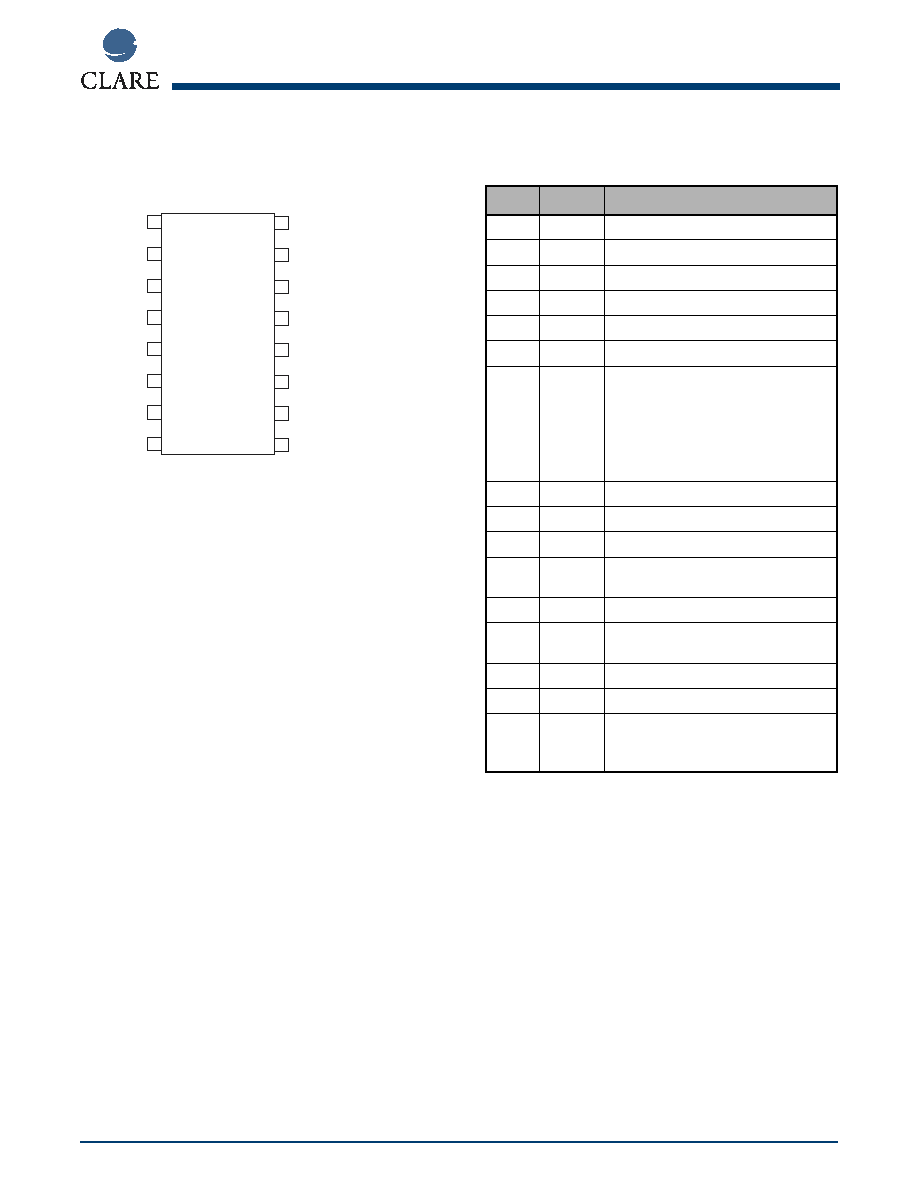
1.1 Package Pinout
1.2 Pinout
CPC7582
1
16
2
15
3
14
4
13
5
12
6
11
7
10
8
9
T
BAT
SD
F
GND
T
LINE
T
RINGING
T
TEST
V
DD
T
D
GND
V
BAT
R
BAT
R
LINE
R
RINGING
R
TEST
LATCH
IN
RINGING
IN
TEST
Pin
Name
Description
1
F
GND
Fault ground
2
T
BAT
Connect to tip on SLIC side
3
T
LINE
Connect to tip on line side
4
T
RINGING
Connect to ringing generator return
5
T
TEST
Connect to test bus tip lead
6
V
DD
+5 V supply
7
T
SD
Temperature shutdown pin. Bi-directional
I/O with internal pullup to V
DD
. Output
function indicates status of thermal
shutdown circuitry. Input function can be
used to set the `all off' mode using an
open-drain type output.
8
D
GND
Digital ground
9
IN
TEST
Logic-level switch control input
10
IN
RINGING
Logic-level switch control input
11
LATCH
Data latch control, active high, transparent
low
12
R
TEST
Connect to test bus ring lead
13
R
RINGING
Connect to ringing generator current
limiting resistor
14
R
LINE
Connect to ring on the line side
15
R
BAT
Connect to ring on the SLIC side
16
V
BAT
Battery voltage supply. Must be capable of
sourcing the trigger current for proper
operation of the protection SCR.
CPC7582
4
www.clare.com
Rev. 3.0 10/4/2002
1.3 Absolute Maximum Ratings (at 25∞ C)
1.4 Electrical Characteristics, T
A
= -40∞ C to +85∞ C
Unless otherwise specified, minimum and maximum
values are production testing requirements. Typical
values are characteristic of the device and are the
result of engineering evaluations. Typical values are
provided for information purposes only and are not
part of the testing requirements.
Absolute maximum ratings are stress ratings. Stresses in
excess of these ratings can cause permanent damage to
the device. Functional operation of the device at these or
any other conditions beyond those indicated in the
operational sections of this data sheet is not implied.
Exposure of the device to the absolute maximum ratings
for an extended period may degrade the device and affect
its reliability.
1.4.1 Power Supply Specifications
1.4.2 Break Switches, SW1 and SW2
Parameter
Minimum Maximum
Unit
Operating temperature
-40
+110
∞C
Storage temperature
-40
+150
∞C
Operating relative humidity
5
95
%
Pin soldering temperature
(10 seconds max)
-
+220
∞C
+5 V power supply (V
DD
)
-0.3
7
V
Battery Supply
-
-85
V
Logic input voltage
-0.3
V
DD
+ 0.3
V
Logic input to switch output
isolation
-
330
V
Switch open contact
isolation (SW1, SW2, SW3,
SW5, SW6)
-
330
V
Switch Open Contact
Isolation (SW4)*
-
480
V
*Ringing supply side of switch limited to ±210 V with respect to ground
Supply
Minimum Typical Maximum
Unit
V
DD
+4.5
+5.0
+5.5
V
V
BAT
1
-19
-
-72
V
1
V
BAT
is used only for internal protection circuitry. If V
BAT
rises above
-10 V, the device will enter the all-off state and will remain in the all-off
state until the battery drops below -15 V.
ESD Rating (Human Body Model)
1000 V
Parameter
Conditions
Symbol
Minimum
Typical
Maximum
Unit
Off-state leakage current
+25∞ C
V
SW
(differential) = -320 V to GND
V
SW
(differential) = +260 V to -60 V
I
SW
-
0.1
1
µ
A
+85∞ C
V
SW
(differential) = -330 V to GND
V
SW
(differential) = +270 V to -60 V
0.3
-40∞ C
V
SW
(differential) = -310 V to GND
V
SW
(differential) = +250 V to -60 V
0.1
R
ON
+25∞ C
I
SW
= ±10 mA, ±40 mA,
R
BAT
and T
BAT
= -2 V
R
ON
-
14.5
-
+85∞ C
20.5
28
-40∞ C
10.5
-
R
ON
match
Per on-resistance test condition of
SW1, SW2.
Magnitude R
ON
SW1 - R
ON
SW2
R
ON
0.15
0.8

CPC7582
Rev. 3.0
10/4/2002
www.clare.com
5
1.4.3 Ringing Return Switch, SW3
DC current limit
+25∞ C
V
SW
(on) = ±10 V
I
SW
-
300
-
mA
+85∞ C
80
160
-
-40∞ C
-
400
425
Dynamic current limit
(t = <0.5
µ
s)
Break switches on, all other switches
off, apply ±1 kV 10/1000
µ
s pulse, with
appropriate protection in place.
-
2.5
-
A
Logic input to switch output isolation
+25∞ C
V
SW
(T
LINE
, R
LINE
) = ±320 V, logic
inputs = gnd
I
SW
-
0.1
1
µ
A
+85∞ C
V
SW
(T
LINE
, R
LINE
) = ±330 V, logic
inputs = gnd
0.3
-40∞ C
V
SW
(T
LINE
, R
LINE
) = ±310 V, logic
inputs = gnd
0.1
dv/dt sensitivity
-
-
200
-
V/
µ
s
Parameter
Conditions
Symbol
Minimum
Typical
Maximum
Unit
Off-state leakage current
+25∞ C
V
SW
(differential) = -320 V to GND
V
SW
(differential) = +260 V to -60 V
I
SW
-
0.1
1
µ
A
+85∞ C
V
SW
(differential) = -330 V to GND
V
SW
(differential) = +270 V to -60 V
0.3
-40∞ C
V
SW
(differential) = -310 V to GND
V
SW
(differential) = +250 V to -60 V
0.1
R
ON
+25∞ C
I
SW
(on) = ±0 mA, ±10 mA
R
ON
-
60
-
+85∞ C
85
100
-40∞ C
45
-
DC current limit
+25∞ C
V
SW
(on) = ±10 V
I
SW
-
135
-
mA
+85∞ C
70
85
-40∞ C
-
210
Dynamic current limit
(t = <0.5
µ
s)
Ringing switches on, all other switches
off, apply ±1 kV 10/1000
µ
s pulse, with
appropriate protection in place.
2.5
A
Logic input to switch output isolation
+25∞ C
V
SW
(T
RINGING
, T
LINE
) = ±320 V, logic
inputs = gnd
I
SW
-
0.1
1
µ
A
+85∞ C
V
SW
(T
RINGING
, T
LINE
) = ±330 V, logic
inputs = gnd
0.3
-40∞ C
V
SW
(T
RINGING
, T
LINE
) = ±310 V, logic
inputs = gnd
0.1
dv/dt sensitivity
-
-
200
-
V/
µ
s
Parameter
Conditions
Symbol
Minimum
Typical
Maximum
Unit
CPC7582
6
www.clare.com
Rev. 3.0 10/4/2002
1.4.4 Ringing Switch, SW4
1.4.5 Test Switches, SW5 and SW6
Parameter
Conditions
Symbol
Minimum
Typical
Maximum
Unit
Off-state leakage current
+25∞ C
V
SW
(differential) = -255 V to +210 V
V
SW
(differential) = +255 V to -210 V
I
SW
-
0.05
1
µ
A
+85∞ C
V
SW
(differential) = -270 V to +210 V
V
SW
(differential) = +270 V to -210 V
0.1
-40∞ C
V
SW
(differential) = -245 V to +210 V
V
SW
(differential) = +245 V to -210 V
0.05
On Voltage
I
SW
(on) = ± 1 mA
-
1.5
3
V
Ringing generator
current to ground during
ringing
V
DD
= 5 V, inputs set for ringing mode
I
RINGING
0.1
0.25
mA
Surge current*
Ringing switches on, all other switches
off, apply ±1 kV 10/1000
µ
s pulse, with
appropriate protection in place.
-
-
2
A
On steady-state current* Inputs set for ringing mode
I
SW
-
150
mA
Release current
-
I
RINGING
300
-
µ
A
R
ON
I
SW
(on) = ±70 mA, ±80 mA
R
ON
10
15
Logic input to switch output isolation
+25∞ C
V
SW
(R
RINGING
, R
LINE
) = ±320 V, logic
inputs = gnd
I
SW
-
0.1
1
µ
A
+85∞ C
V
SW
(R
RINGING
, R
LINE
) = ±330 V, logic
inputs = gnd
0.3
-40∞ C
V
SW
(R
RINGING
, R
LINE
) = ±310 V, logic
inputs = gnd
0.1
dv/dt sensitivity
-
-
200
-
V/
µ
s
*Secondary protection and ringing source current limiting must prevent exceeding this parameter.
Parameter
Conditions
Symbol
Minimum
Typical
Maximum
Unit
Off-state leakage current
+25∞ C
V
SW
(differential) = -320 V to GND
V
SW
(differential) = +260 V to -60 V
I
SW
-
0.1
1
µ
A
+85∞ C
V
SW
(differential) = -330 V to GND
V
SW
(differential) = +270 V to -60 V
0.3
-40∞ C
V
SW
(differential) = -310 V to GND
V
SW
(differential) = +250 V to -60 V
0.1
CPC7582
Rev. 3.0
10/4/2002
www.clare.com
7
1.5 Additional Electrical Characteristics
R
ON
+25∞ C
I
SW(ON)
= ±10 mA, ±40 mA,
T
BAT
= -2 V
R
ON
-
38
-
+85∞ C
46
70
-40∞ C
28
-
DC current limit
+25∞ C
V
SW
(on) = ±10 V
I
SW
-
175
-
mA
+85∞ C
80
110
-
-40∞ C
-
210
250
Dynamic current limit
(t = <0.5
µ
s)
Test switches on, all other switches off,
apply ±1 kV at 10/1000
µ
s pulse, with
appropriate protection in place.
-
2.5
-
A
Logic input to switch output isolation
+25∞ C
V
SW
(T
TEST
, T
LINE
) = ±320 V,
logic inputs = gnd
I
SW
-
0.1
1
µ
A
+85∞ C
V
SW
(T
TEST
, T
LINE
) = ±330 V,
logic inputs = gnd
0.3
-40∞ C
V
SW
(T
TEST
, T
LINE
) = ±310 V,
logic inputs = gnd
0.1
Parameter
Conditions
Symbol
Minimum
Typical
Maximum
Unit
Parameter
Conditions
Symbol
Minimum
Typical
Maximum
Unit
Digital input characteristics
Input low voltage
-
V
IL
-
-
1.5
V
Input high voltage
-
V
IH
3.5
-
-
Input leakage current
(high)
V
DD
= 5.5 V, V
BAT
= -75 V, V
IH
= 5 V
I
IH
-
0.1
1
µ
A
Input leakage current
(low)
V
DD
= 5.5 V, V
BAT
= -75 V, V
IL
= 0 V
I
IL
-
0.1
1
Power requirements
Power consumption in
talk and all-off states
V
DD
= 5 V, V
BAT
= -48 V, measure I
DD
and I
BAT
P
-
5.5
10
mW
Power consumption in
all other states
6.5
10
V
DD
current in talk and
all-off states
V
DD
= 5 V, V
BAT
= -48 V
I
DD
-
1.1
2.0
mA
V
DD
current in all other
states
I
DD
-
1.3
2.0
V
BAT
current in any
state
V
DD
= 5 V, V
BAT
= -48 V
I
BAT
-
0.1
10
µ
A
Temperature Shutdown Requirements (temperature shutdown flag is active low)
Shutdown activation
temperature
-
-
110
125
150
∞C
Shutdown circuit
hysteresis
-
-
10
-
25
∞C

CPC7582
8
www.clare.com
Rev. 3.0 10/4/2002
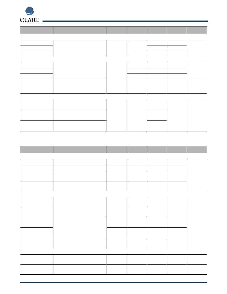
1.6 Protection Circuitry Electrical Specifications
1.7 CPC7582xA/B Truth Table
Parameter
Conditions
Symbol
Minimum
Typical
Maximum
Unit
Parameters Related to the Diodes in the Diode Bridge
Voltage drop at
continuous current
(50/60 Hz)
Apply ± dc current limit of break
switches
Forward
Voltage
-
2.1
3
V
Voltage drop at surge
current
Apply ± dynamic current limit of
break switches
Forward
Voltage
-
5
-
Parameters Related to the Protection SCR
Surge current
-
-
-
-
*
A
Trigger current (+25∞ C)
I
TRIG
-
60 (CPC7582xA, xB)
70 (CPC7582xC)
-
mA
Trigger current (+85∞ C)
-
35 (CPC7582xA, xB)
40 (CPC7582xC)
-
Hold current (+25∞ C)
I
HOLD
-
100 (CPC7582xA, xB)
135 (CPC7582xC)
-
Hold current (+85∞ C)
60 (CPC7582xA, xB)
110 (CPC7582xC)
70 (CPC7582xA, xB)
115 (CPC7582xC)
-
Gate trigger voltage
I
GATE
= I
TRIGGER
**
V
TBAT
or
V
RBAT
V
BAT
-4
-
V
BAT
-2
V
Reverse leakage
current
V
BAT
= -48 V
I
VBAT
-
-
1.0
µ
A
On-state voltage
0.5 A, t = 0.5 ms
V
TBAT
or
V
RBAT
-
-3
-
V
2.0 A, t = 0.5 ms
V
TBAT
or
V
RBAT
-
-5
-
V
*Passes GR1089 and ITU-T K.20 with appropriate secondary protection in place.
**V
BAT
must be capable of sourcing I
TRIGGER
for the internal SCR to activate.
State
IN
RINGING
IN
TEST
LATCH
T
SD
Break
Switches
Ringing
Switches
Test
Switches
Talk
0
0
0
1 or
Floating
1
On
Off
Off
Test
0
1
Off
Off
On
Ringing
1
0
Off
On
Off
All Off
1
1
Off
Off
Off
Latched
X
X
1
Unchanged
All off
X
X
X
0
2
Off
Off
Off
1
If T
SD
is tied high, thermal shutdown is disabled. If T
SD
is left floating, the thermal shutdown mechanism functions normally.
2
Forcing T
SD
to ground overrides the logic input pins and forces an all off state.
CPC7582
Rev. 3.0
10/4/2002
www.clare.com
9
1.8 CPC7582xC Truth Table
2. Functional Description
2.1 Introduction
2.1.1 CPC7582xA/B Logic States
∑
Talk. Break switches SW1 and SW2 closed, ringing
switches SW3 and SW4 open, and test switches
SW5 and SW6 open.
∑
Ringing. Break switches SW1 and SW2 open,
ringing switches SW3 and SW4 closed, and test
switches SW5 and SW6 open.
∑
Test. Break switches SW1 and SW2 open, ringing
switches SW3 and SW4 open, and loop test
switches SW5 and SW6 closed.
∑
All off. Break switches SW1 and SW2 open, ringing
switches SW3 and SW4 open, and test switches
SW5 and SW6 open.
2.1.2 CPC7582xC Logic States:
∑
Talk. Break switches SW1 and SW2 closed, ringing
switches SW3 and SW4 open, and test switches
SW5 and SW6 open.
∑
Ringing. Break switches SW1 and SW2 open,
ringing switches SW3 and SW4 closed, and test
switches SW5 and SW6 open.
∑
Test/Monitor. Break switches SW1 and SW2
closed, ringing switches SW3 and SW4 open, and
test switches SW5 and SW6 closed.
∑
Ringing Test. Break switches SW1 and SW2 open,
ringing switches SW3 and SW4 closed, and test
switches SW5 and SW6 closed.
∑
All off. Break switches SW1 and SW2 open, ringing
switches SW3 and SW4 open, and test switches
SW5 and SW6 open.
The CPC7582 offers break-before-make and make-
before-break switching from the ringing state to the
talk state with simple logic-level input control. Solid-
state switch construction means no impulse noise is
generated when switching during ring cadence or ring
trip, eliminating the need for external zero-cross
switching circuitry. State control is via logic-level input
so no additional driver circuitry is required. The linear
break switches SW1 and SW2 have exceptionally low
R
ON
and excellent matching characteristics. The
ringing switch SW4 has a minimum open contact
breakdown voltage of 480 V. This is sufficiently high,
with proper protection, to prevent breakdown in the
presence of a transient fault condition (i.e., passing
the transient on to the ringing generator).
Integrated into the CPC7582 is an over voltage
clamping circuit, active current limiting, and a thermal
shutdown mechanism to provide protection to the
SLIC device during a fault condition. Positive and
negative surges are reduced by the current limiting
circuitry and hazardous potentials are diverted to
ground via diodes and, in xA/C parts, an integrated
SCR. Power-cross potentials are also reduced by the
current limiting and thermal shutdown circuits.
To protect the CPC7582 from an overvoltage fault
condition, use of a secondary protector is required.
The secondary protector must limit the voltage seen at
the tip and ring terminals to a level below the
maximum breakdown voltage of the switches. To
minimize the stress on the solid-state contacts, use of
a foldback or crowbar type secondary protector is
recommended. With proper selection of the secondary
protector, a line card using the CPC7582BC will meet
all relevant ITU, LSSGR, TIA/EIA and IEC protection
requirements.
The CPC7582 operates from a +5 V supply only. This
gives the device extremely low idle and active power
consumption and allows use with virtually any range of
State
IN
RINGING
IN
TEST
LATCH
T
SD
Break
Switches
Ringing
Switches
Test
Switches
Talk
0
0
0
1 or
Floating
1
On
Off
Off
Test/Monitor
0
1
On
Off
On
Ringing
1
0
Off
On
Off
Ringing Test
1
1
Off
On
On
Latched
X
X
1
Unchanged
All off
X
X
X
0
2
Off
Off
Off
1
If T
SD
is tied high, thermal shutdown is disabled. If T
SD
is left floating, the thermal shutdown mechanism functions normally.
2
Forcing T
SD
to ground overrides the logic input pins and forces an all off state.
CPC7582
10
www.clare.com
Rev. 3.0 10/4/2002
battery voltage. Battery voltage is also used by the
CPC7582 as a reference for the integrated protection
circuit. In the event of a loss of battery voltage, the
CPC7582 enters the all-off state.
2.2 Switch Logic
The CPC7582 provides, when switching from the
ringing state to the talk state, the ability to control the
release timing of the ringing switches SW3 and SW4
relative to the state of the break switches SW1 and
SW2 using simple logic-level inputs. This is referred to
as make-before-break or break-before-make
operation. When the break switch contacts (SW1 and
SW2) are closed (or made) before the ringing switch
contacts (SW3 and SW4) are opened (or broken), this
is referred to as make-before-break operation. Break-
before-make operation occurs when the ringing
contacts (SW3 and SW4) are opened (broken) before
the break switch contacts (SW1 and SW2) are closed
(made). With the CPC7582, the make-before-break
and break-before-make operations can easily be
selected by applying logic-level inputs to the device.
The logic sequences for these modes of operation are
given in "Make-Before-Break Operation for All
Versions (Ringing to Talk Transition)" on page 10,
"Break-Before-Make Operation CPC7582xA/B
(Ringing to Talk Transition)" on page 11, and "Break-
Before-Make Operation for all Version (Ringing to Talk
Transition)" on page 11. Logic states and input control
settings are given in "CPC7582xA/B Truth Table" on
page 8 and "CPC7582xC Truth Table" on page 9.
2.2.1 Make-Before-Break Operation - All Versions
To use make-before-break operation, change the logic
inputs to the talk state immediately following the
ringing state. Application of the talk state opens the
ringing return switch (SW3) as the break switches
(SW1 and SW2) close. The ringing switch (SW4)
remains open until the next zero-crossing of the
ringing supply current. While in the make-before-break
state, ringing potentials in excess of the CPC7582
protection circuitry trigger levels will be diverted to
ground.
2.2.2 Make-Before-Break Operation for All Versions (Ringing to Talk Transition)
2.2.3 Break-Before-Make Operation - CPC7582xA/B
Break-before-make operation of the CPC7582xA/B
can be achieved using two different techniques.
The first method uses manipulation of the IN
RINGING
and IN
TEST
logic inputs as shown in "Break-Before-
Make Operation CPC7582xA/B (Ringing to Talk
Transition)" on page 11.
1.
At the end of the ringing state apply the all off
state (0, 0). This releases the ringing return
switch (SW3) while the ringing switch remains
on, waiting for the next zero current event.
2.
Hold the all off state for at least one-half of a
ringing cycle to assure that a zero crossing event
occurs and that the ringing switch (SW4) has
opened.
Break-before-make operation occurs when the ringing
switch opens before the break switches (SW1 and
SW2) close.
State
IN
RINGING
IN
TEST
LATCH
T
SD
Timing
Break
Switches
Ringing
Return
Switch
(SW3)
Ringing
Switch
(SW4)
Test
Switches
Ringing
1
0
0
Floating
-
Off
On
On
Off
Make-
before-
break
0
0
SW4 waiting for next zero-current
crossing to turn off. Maximum time is
one-half of the ringing cycle. In this
transition state, current that is limited to
the dc break switch current limit value
will be sourced from the ring node of the
SLIC.
On
Off
On
Off
Talk
0
0
Zero-cross current has occurred
On
Off
Off
Off

CPC7582
Rev. 3.0
10/4/2002
www.clare.com
11
2.2.4 Break-Before-Make Operation CPC7582xA/B (Ringing to Talk Transition)
2.2.5 Break-Before-Make Operation - All Versions
The second break-before-make method for the
CPC7582xA/B is also the only method available for
the CPC7582xC. As shown in "CPC7582xA/B Truth
Table" on page 8 and "CPC7582xC Truth Table" on
page 9, the bi-directional T
SD
interface disables all of
the CPC7582 switches when pulled to a logic low.
Although logically disabled, if the ringing switch (SW4)
is active (closed), it will remain closed until the next
current zero crossing event.
As shown in the table "Break-Before-Make Operation
for all Version (Ringing to Talk Transition)" on
page 11, this operation is similar to the one shown in
"Break-Before-Make Operation - All Versions" on
page 11, except in the method used to select the all off
state, and in when the IN
RINGING
and IN
TEST
inputs
are reconfigured for the talk state.
1.
Pull T
SD
to a logic low to end the ringing state.
This opens the ringing return switch (SW3) and
prevents any other switches from closing.
2.
Keep T
SD
low for at least one-half the duration of
the ringing cycle period to allow sufficient time for
a zero crossing current event to occur and for the
circuit to enter the break before make state.
3.
During the T
SD
low period, set the IN
RINGING
and
IN
TEST
inputs to the talk state (0, 0).
4.
Release T
SD
, allowing the internal pull-up to
activate the break switches.
When using T
SD
as an input, the two recommended
states are 0 (overrides logic input pins and forces an
all off state) and float (allows switch control via logic
input pins and the thermal shutdown mechanism is
active). This requires the use of an open-collector type
buffer.
Forcing T
SD
to a logic high disables the thermal
shutdown circuit and is therefore not recommended as
this could lead to device damage or destruction in the
presence of excessive tip or ring potentials.
2.2.6 Break-Before-Make Operation for all Version (Ringing to Talk Transition)
State
IN
RINGING
IN
TEST
LATCH
T
SD
Timing
Break
Switches
Ringing
Return
Switch
(SW3)
Ringing
Switch
(SW4)
Test
Switches
Ringing
1
0
0
Floating
-
Off
On
On
Off
All-Off
1
1
Hold this state for at least one-half of the
ringing cycle. SW4 waiting for zero
current to turn off.
Off
Off
On
Off
Break-
Before-
Make
1
1
SW4 has opened
Off
Off
Off
Off
Talk
0
0
Close Break Switches
On
Off
Off
Off
State
IN
RINGING
IN
TEST
LATCH
T
SD
Timing
Break
Switches
Ringing
Return
Switch
(SW3)
Ringing
Switch
(SW4)
Test
Switches
Ringing
1
0
0
Floating
-
Off
On
On
Off
All-Off
0
0
0
Hold this state for at least one-half of the
ringing cycle. SW4 waiting for zero
current to turn off.
Off
Off
On
Off
Break-
Before-
Make
0
0
SW4 has opened
Off
Off
Off
Off
Talk
0
0
Floating
Close Break Switches
On
Off
Off
Off

CPC7582
12
www.clare.com
Rev. 3.0 10/4/2002
2.3 Data Latch
The CPC7582 has an integrated data latch. The latch
operation is controlled by logic-level input pin 11
(LATCH). The data input of the latch is pin 10
(IN
RINGING
) and pin 9 (IN
TEST
) of the device while the
output of the data latch is an internal node used for
state control. When LATCH control pin is at logic 0,
the data latch is transparent and data control signals
flow directly through to state control. A change in input
will be reflected in the switch state. When LATCH
control pin is at logic 1, the data latch is active and a
change in input control will not affect switch state. The
switches will remain in the position they were in when
the LATCH changed from logic 0 to logic 1 and will not
respond to changes in input as long as the latch is at
logic 1. The T
SD
input is not tied to the data latch.
Therefore, T
SD
is not affected by the LATCH input and
the T
SD
input will override state control.
2.4 T
SD
Setting T
SD
to +5 V allows switch control using the
logic inputs. This setting, however, also disables the
thermal shutdown circuit and is therefore not recom-
mended. When using logic controls via the input pins,
pin 7 (T
SD
) should be allowed to float. As a result, the
two recommended states when using pin 7 (T
SD
) as a
control are 0, which forces the device to the all-off
state, or float, which allows logic inputs to remain
active. This requires the use of an open-collector type
buffer.
2.5 Ringing Switch Zero-Cross Current Turn Off
After the application of a logic input to turn SW4 off,
the ringing switch is designed to delay the change in
state until the next zero-crossing. Once on, the switch
requires a zero-current cross to turn off, and therefore
should not be used to switch a pure DC signal. The
switch will remain in the on state no matter the logic
input until the next zero crossing. These switching
characteristics will reduce and possibly eliminate
overall system impulse noise normally associated with
ringing switches. See application note AN-144,
Impulse Noise Benefits of Line Card Access Switches
. The
attributes of ringing switch SW4 may make it possible
to eliminate the need for a zero-cross switching
scheme. A minimum impedance of 300
in series
with the ringing generator is recommended.
2.6 Power Supplies
Both a +5 V supply and battery voltage are connected
to the CPC7582. CPC7582 switch state control is
powered exclusively by the +5 V supply. As a result,
the CPC7582BC exhibits extremely low power
dissipation during both active and idle states.
The battery voltage is not used for switch control but
rather as a supply for the integrated secondary
protection circuitry. The integrated SCR is designed to
trigger when pin 2 (T
BAT
) or pin 15 (R
BAT
) drops 2 to
4 V below the voltage on pin 16 (V
BAT
). This trigger
prevents a fault induced overvoltage event at the T
BAT
or R
BAT
nodes.
2.7 Battery Voltage Monitor
The CPC7582 also uses the V
BAT
voltage to monitor
battery voltage. If battery voltage is lost, the CPC7582
immediately enters the all-off state. It remains in this
state until the battery voltage is restored. The device
also enters the all-off state if the battery voltage rises
above ≠10 V and remains in the all-off state until the
battery voltage drops below ≠15 V. This battery
monitor feature draws a small current from the battery
(less than 1
µ
A typical) and will add slightly to the
device's overall power dissipation.
2.8 Protection
2.8.1 Diode Bridge/SCR
The CPC7582 uses a combination of current limited
break switches, a diode bridge/SCR clamping circuit,
and a thermal shutdown mechanism to protect the
SLIC device or other associated circuitry from damage
during line transient events such as lightning. During a
positive transient condition, the fault current is
conducted through the diode bridge to ground via
F
GND
. Voltage is clamped to a diode drop above
ground. During a negative transient of 2 to 4 V more
negative than the voltage at V
BAT
, the SCR conducts
and faults are shunted to F
GND
via the SCR or the
diode bridge.
In order for the SCR to crowbar or foldback, the on
voltage (see "Protection Circuitry Electrical
Specifications" on page 8) of the SCR must be less
negative than the V
BAT
voltage. If the V
BAT
voltage is
less negative than the SCR on voltage or if the V
BAT
supply is unable to source the trigger current, the SCR
will not crowbar.
For power induction or power-cross fault conditions,
the positive cycle of the transient is clamped to the
diode drop above ground and the fault current directed
to ground. The negative cycle of the transient will
cause the SCR to conduct when the voltage exceeds

CPC7582
Rev. 3.0
10/4/2002
www.clare.com
13
the V
BAT
voltage by two to four volts, steering the
current to ground.
2.8.2 Current Limiting function
If a lightning strike transient occurs when the device is
in the talk state, the current is passed along the line to
the integrated protection circuitry and limited by the
dynamic current limit response of the active switches
during the talk state. During the talk state, when a
1000V 10/1000
µ
s pulse (GR-1089-CORE lightning) is
applied to the line though a properly clamped external
protector, the current seen at pins 2 (T
BAT
) and pin 15
(R
BAT
) will be a pulse with a typical magnitude of 2.5 A
and a duration of less than 0.5
µ
s.
If a power-cross fault occurs with the device in the talk
state, the current is passed though break switches
SW1 and SW2 on to the integrated protection circuit
and is limited by the dynamic DC current limit
response of the two break switches. The DC current
limit, specified over temperature, is between 80 mA
and 425 mA, and the circuitry has a negative
temperature coefficient. As a result, if the device is
subjected to extended heating due to a power cross
fault, the measured current at pin 3 (T
LINE
) and pin 14
(R
LINE
) will decrease as the device temperature
increases. If the device temperature rises sufficiently,
the temperature shutdown mechanism will activate
and the device will enter the all-off state.
2.9 Temperature Shutdown
The thermal shutdown mechanism will activate when
the device temperature reaches a minimum of 110∞ C,
placing the device in the all-off state regardless of
logic input. During thermal shutdown mode, pin 7
(T
SD
) will read 0 V. Normal output of T
SD
is +V
DD
.
If presented with a short duration transient such as a
lightning event, the thermal shutdown feature will
typically not activate. But in an extended power-cross
transient, the device temperature will rise and the
thermal shutdown will activate forcing the switches to
the all-off state. At this point the current measured at
pin 3 (T
LINE
) and pin 14 (R
LINE
) will drop to zero. Once
the device enters thermal shutdown it will remain in
the all-off state until the temperature of the device
drops below the de-activation level of the thermal
shutdown circuit. This will permit the device to return
to normal operation. If the transient has not passed,
current will flow at the value allowed by the dynamic
DC current limiting of the switches and heating will
begin again, reactivating the thermal shutdown
mechanism. This cycle of entering and exiting the
thermal shutdown mode will continue as long as the
fault condition persists. If the magnitude of the fault
condition is great enough, the external secondary
protector could activate and shunt all current to
ground.
The thermal shutdown mechanism of the CPC7582
can be disable by applying a logic high to pin 7 (T
SD
).
2.10 External Protection Elements
The CPC7582 requires only overvoltage secondary
protection on the loop side of the device. The
integrated protection feature described above negates
the need for protection on the line side. The secondary
protector limits voltage transients to levels that do not
exceed the breakdown voltage or input-output
isolation barrier of the CPC7582. A foldback or
crowbar type protector is recommended to minimize
stresses on the device.
Consult Clare's application note, AN-100, "
Designing
Surge and Power Fault Protection Circuits for Solid
State Subscriber Line Interfaces
" for equations related
to the specifications of external secondary protectors,
fused resistors and PTCs.
CPC7582
14
www.clare.com
Rev. 3.0 10/4/2002
3. Manufacturing Information
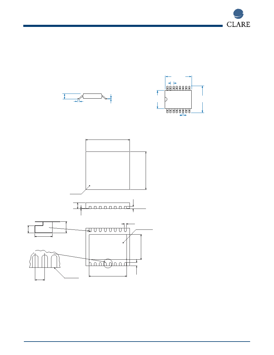
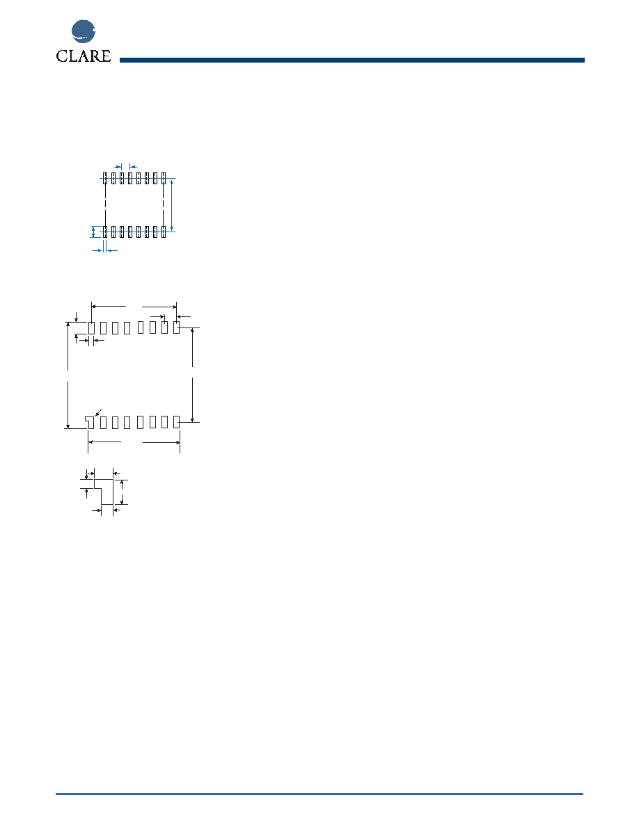
3.1 Mechanical Dimensions
3.1.1 SOIC
3.1.2 MLP
7.40 MIN / 7.60 MAX
(.291 MIN / .299 MAX)
0.23 MIN / 0.32 MAX
(.0091 MIN / .0125 MAX)
1.27
(.050)
2.44 MIN / 2.64 MAX
(.096 MIN / .104 MAX)
0.51 MIN / 1.01 MAX
(.020 MIN / .040 MAX)
10.11 MIN / 10.51 MAX
(.398 MIN / .414 MAX)
0.36 MIN / 0.46 MAX
(.014 MIN / .018 MAX)
10.11 MIN / 10.31 MAX
(.398 MIN / .406 MAX)
16 Pin SOIC (JEDEC Package)
0.55
0.80
0.23
0.55
0.33
(+0.07, -0.05)
0.2
0.80
(±0.10)
0.02
(+0.05, -0)
Terminal Tip
INDEX AREA
SEATING
PLANE
EXPOSED PAD
TOP VIEW
SIDE VIEW
BOTTOM VIEW
16
1
2
7
6
4.0
(±0.05)
6.0
(±0.05)
0.55
(±0.1)
Dimensions in mm
CPC7582
Rev. 3.0
10/4/2002
www.clare.com
15
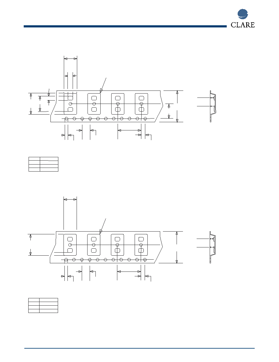
3.2 Printed-Circuit Board Layout
3.2.1 SOIC
3.2.2 MLP
NOTE: For optimum solder joint size, MLP package
printed-circuit board pads should extend no more than
.05 mm past the chip post on the short sides, and no
more than .025 mm past the chip posts on the long
sides.
As the metallic pad on the bottom of the MLP package
is connected to the substrate of the die, Clare
recommends that no printed circuit board traces or
vias be placed under this area to maintain minimum
creepage and clearance values.
PC Board Pattern
(Top View)
1.193
(.047)
9.728
±
.051
(.383
±
.002)
.787
(.031)
1.270
(.050)
0.65
6.1
0.38
0.65
0.38
0.47
0.66
5.75
6.13
0.75 on center
5.35 on center
Detail A
Detail A
All dimensions in mm
Not drawn to scale
CPC7582
16
www.clare.com
Rev. 3.0 10/4/2002
3.3 Tape and Reel Packaging
3.3.1 SOIC
3.3.2 MLP
B0
16.00
7.50
R = .50
2.30
K0
K1
1.30
6.80
3.00
A0
2.00
4.00
2.00
1.50
12.00
6.50
2.70
A0 =
B0 =
K0 =
K1 =
NOTES: 1. ALL DIMENSIONS ARE IN MILLIMETERS AND CARRY TOLERANCES OF EIA
STANDARD 481-2. 2. THE TAPE COMPLIES WITH ALL "NOTES" FOR CONSTANT DIMENSIONS
LISTED ON PAGE 5 OF EIA-481-2.
6.5 mm
10.3 mm
2.3 mm
2.7 mm
B0
16.00
R = .50
1.4
K0
K1
7.40
A0
4.00
2.00
1.50
12.00
6.4
1.4
A0 =
B0 =
K0 =
K1 =
NOTES:1. ALL DIMENSIONS ARE IN MILLIMETERS AND CARRY TOLERANCES OF EIA
STANDARD 481-2. 2. THE TAPE COMPLIES WITH ALL "NOTES" FOR CONSTANT DIMENSIONS
LISTED ON PAGE 5 OF EIA-481-2.
6.4 mm
7.4 mm
1.4 mm
1.4 mm

3.4 Soldering
3.4.1 Moisture Reflow Sensitivity
Clare has characterized the moisture reflow sensitivity
of LCAS products using IPC/JEDEC standard
J-STD-020A. Moisture uptake from atmospheric
humidity occurs by diffusion. During the solder reflow
process, in which the component is attached to the
PCB, the whole body of the component is exposed to
high process temperatures. The combination of
moisture uptake and high reflow soldering
temperatures may lead to moisture induced
delamination and cracking of the component. To
prevent this, this component must be handled in
accordance with IPC/JEDEC standard J-STD-020A
per the labelled moisture sensitivity level (MSL), level
1 for the SOIC package, and level 3 for the MLP
package.
3.4.2 Reflow Profile
The maximum ramp rates, dwell times, and
temperatures of the assembly reflow profile should not
exceed those specified in IPC standard IPC-9502,
table 2. Soldering processes are limited to 220 ∞C
component body temperature.
3.5 Washing
Clare does not recommend ultrasonic cleaning of
LCAS parts.
For additional information please visit
www.clare.com
Clare, Inc. makes no representations or warranties with respect to the accuracy or completeness of the contents of this publication and reserves the right to make
changes to specifications and product descriptions at any time without notice. Neither circuit patent licenses or indemnity are expressed or implied. Except as set
forth in Clare's Standard Terms and Conditions of Sale, Clare, Inc. assumes no liability whatsoever, and disclaims any express or implied warranty relating to its
products, including, but not limited to, the implied warranty of merchantability, fitness for a particular purpose, or infringement of any intellectual property right.
The products described in this document are not designed, intended, authorized, or warranted for use as components in systems intended for surgical implant into
the body, or in other applications intended to support or sustain life, or where malfunction of Clare's product may result in direct physical harm, injury, or death to a
person or severe property or environmental damage. Clare, Inc. reserves the right to discontinue or make changes to its products at any time without notice.
Specifications: DS-CPC7582-R3.0
© Copyright 2002, Clare, Inc.
All rights reserved. Printed in USA.
10/4/2002