 | –≠–ª–µ–∫—Ç—Ä–æ–Ω–Ω—ã–π –∫–æ–º–ø–æ–Ω–µ–Ω—Ç: IAD112N | –°–∫–∞—á–∞—Ç—å:  PDF PDF  ZIP ZIP |
1
www.clare.com
IAD112N
DS-IAD112N-R2
The IAD112N Multifunction Telecom switch combines a
350V Form A relay and two optocouplers in a single pack-
age. The relay uses optically coupled MOSFET technolo-
gy to provide 1500V of input to output isolation. The
efficient MOSFET switch and photovoltaic die use Clare's
patented OptoMOS architecture. The optically coupled
input uses highly efficient GaAIAs infrared LEDs.
IAD112N's allow telecom circuit designers to combine
three discrete functions in a single component. The
IAD112N's small package uses less space than tradition-
al discrete component solutions.
∑
Telecommunications
∑
Telecom Switching
∑
Tip/Ring Circuits
∑
Modem Switching (Laptop, Notebook, Pocket Size)
∑
Hookswitch
∑
Dial Pulsing
∑
Ground Start
∑
Ringer Injection
∑
Instrumentation
∑
Multiplexers
∑
Data Acquisition
∑
Electronic Switching
∑
I/O Subsystems
∑
Meters (Watt-Hour, Water, Gas)
∑
Medical Equipment-Patient/Equipment Isolation
∑
Security
∑
Aerospace
∑
Industrial Controls
∑
UL Recognized: File Number E76270
∑
CSA Certified: File Number LR 43639-12
∑
VDE Compatible
∑
BSI Certified:
∑
BS EN 60950:1992 (BS7002:1992)
Certificate #:7969
∑
BS EN 41003:1993
Certificate #:7969
∑
16 Pin Narrow SOIC Package
∑
Three Functions in One Package
∑
Bi-Directional Current Sensing
∑
Bi-Directional Current Switching
∑
3750V
RMS
Input/Output Isolation
∑
FCC Compatible
∑
No EMI/RFI Generation
∑
Machine Insertable, Wave Solderable
∑
Tape & Reel Versions Available
Applications
Features
Description
Approvals
Integrated Telecom Circuits
Ordering Information
Part #
Description
IAD112N
16 Pin SOIC (Narrow) (50/Tube)
IAD112N
16 Pin SOIC (Narrow) (1000/Reel)
IAD112N
Units
Load Voltage
350
V
Load Current
100
mA
Max R
ON
35
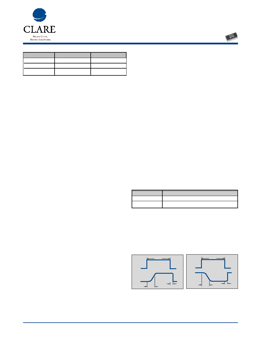
Pin Configuration
Switching Characteristics of
Normally Closed (Form B) Devices
CONTROL
10ms
10%
90%
90%
+
+
T
ON
T
OFF
+
Switching Characteristics of
Normally Open (Form A) Devices
CONTROL
LOAD
10ms
10%
10%
90%
+
T
ON
T
OFF
+
+
www.clare.com
IAD112N
Rev. 2
Absolute Maximum Ratings are stress ratings. Stresses
in excess of these ratings can cause permanent damage
to the device. Functional operation of the device at these
or any other conditions beyond those indicated in the
operational sections of this data sheet is not implied.
Exposure of the device to the absolute maximum ratings
for an extended period may degrade the device and effect
its reliability.
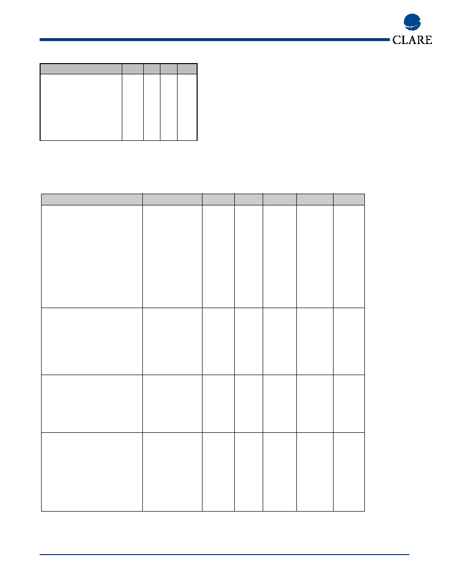
Absolute Maximum Ratings (@ 25∞ C)
2
Parameter
Min
Typ
Max Units
Total Package Dissipation
-
-
1
1
W
Isolation Voltage
Input to Output
3750
-
-
V
RMS
Operational Temperature
-40
-
+85
∞C
Storage Temperature
-40
-
+125
∞C
Soldering Temperature
-
-
+220
∞C
(10 Seconds Max.)
1
Above 25∞ derate linerity 1.67mw/∞C
Electrical Characteristics
Parameter
Conditions
Symbol
Min
Typ
Max
Units
Relay Portion
Output Characteristics @ 25∞C
Load Voltage (Peak)
I
L
= 1µA
V
L
-
-
350
V
Load Current (Continuous)
-
I
L
-
-
100
mA
Peak Load Current
10ms
I
LPK
-
-
350
mA
On-Resistance
I
L
=100mA
R
ON
-
-
35
Off-State Leakage Current
V
L
=350V; T
J
=25∞C
I
LEAK
-
-
1
µA
Switching Speeds
Turn-On
I
F
=5mA, V
L
=10V
T
ON
-
-
3
ms
Turn-Off
I
F
=5mA, V
L
=10V
T
OFF
-
-
3
ms
Output Capacitance
V
L
=50V, f=1MHz
-
-
25
-
pF
Relay Portion
Input Characteristics @ 25∞C
Input Control Current
I
L
=100mA
I
F
5
-
50
mA
Input Dropout Current
I
L
=1mA
I
F
0.4
-
-
mA
Input Voltage Drop
I
F
=5mA
V
F
0.9
1.2
1.4
V
Reverse Input Voltage
-
V
R
-
-
5
V
Reverse Input Current
V
R
=5V
I
R
-
-
10
µA
Detector Portion
Output Characteristics @ 25∞C
Phototransistor Blocking Voltage
I
C
=10µA
BV
CEO
20
50
-
V
Phototransistor Dark Current
VCE=5V, I
F
=0mA
I
CEO
-
50
500
nA
Saturation Voltage
I
C
=2mA, I
F
=16mA
V
SAT
-
0.3
0.5
V
Current Transfer Ratio
I
F
=6mA, V
CE
=0.5V
C
TR
33
-
-
%
Detector Portion
Input Characteristics @ 25∞C
Input Control Current
I
C
=2mA,VCE=0.5V I
F
6
2
-
mA
Input Voltage Drop
IF=5mA
I
CEO
0.9
1.2
1.4
V
Input Current
I
C
=1µA, VCE=5V
-
5
25
-
µA
(Detector must be off)
Input to Output Capacitance
V
L
=50V, f=1MHz
C
I/O
-
3
-
pF
Input to Output Isolation
-
V
I/O
3750
-
-
V
RMS

IAD112N
3
Rev. 2
Dimensions
mm
(inches)
Mechanical Dimensions
.20
± .025
(.008
± .001)
1.27 TYP.
(.050 TYP.)
2.18 MAX.
(.086)
1.01
± .025
(.040
± .001)
3.81
± .05
(.150
± .002)
6.09
± .10
(.240
± .004)
.38 x 45
∞
(.015 x 45
∞)
.38 TYP.
(.015 TYP.)
9.93
± .12
(.391
± .005)
16 Pin SOIC Narrow ("N" Suffix)
PC Board Pattern
(Top View)
1.270
(0.050)
5.080
± .127
(.200
± .005)
1.193
(.047)
.787
(.031)
7.49
(.295)
2.00
(.079)
12.09
(.476)
1.75
(.069)
3.99
(.157)
1.50
(.059)
6.73
(.265)
.41
(.016)
2.30
(.091)
2.70
(.106)
Top Cover
Tape
2.01
(.079)
11.99
(.472)
User Direction of Feed
.05R TYP.
16.00
(.630)
10.30
(.406)
Embossment
Embossed Carrier
Top Cover
Tape Thickness
.10 MAX.
(.004)
6.80
(.268)
6.50
(.256)
3.00
(.118)
1.55
± .102
(.061
± .004)
330.2 DIA.
(13.00)
Tape and Reel Packaging for 8 and 16 Pin Narrow SOIC Package
1
CLARE LOCATIONS
Clare Headquarters
78 Cherry Hill Drive
Beverly, MA 01915
Tel: 1-978-524-6700
Fax: 1-978-524-4900
Toll Free: 1-800-27-CLARE
Clare Micronix Division
145 Columbia
Aliso Viejo, CA 92656-1490
Tel: 1-949-831-4622
Fax: 1-949-831-4628
SALES OFFICES
AMERICAS
Americas Headquarters
Clare
78 Cherry Hill Drive
Beverly, MA 01915
Tel: 1-978-524-6700
Fax: 1-978-524-4900
Toll Free: 1-800-27-CLARE
Eastern Region
Clare
P.O. Box 856
Mahwah, NJ 07430
Tel: 1-201-236-0101
Fax: 1-201-236-8685
Toll Free: 1-800-27-CLARE
Central Region
Clare Canada Ltd.
3425 Harvester Road, Suite 202
Burlington, Ontario L7N 3N1
Tel: 1-905-333-9066
Fax: 1-905-333-1824
Western Region
Clare
1852 West 11th Street, #348
Tracy, CA 95376
Tel: 1-209-832-4367
Fax: 1-209-832-4732
Toll Free: 1-800-27-CLARE
Canada
Clare Canada Ltd.
3425 Harvester Road, Suite 202
Burlington, Ontario L7N 3N1
Tel: 1-905-333-9066
Fax: 1-905-333-1824
EUROPE
European Headquarters
CP Clare nv
Bampslaan 17
B-3500 Hasselt (Belgium)
Tel: 32-11-300868
Fax: 32-11-300890
France
Clare France Sales
Lead Rep
99 route de Versailles
91160 Champlan
France
Tel: 33 1 69 79 93 50
Fax: 33 1 69 79 93 59
Germany
Clare Germany Sales
ActiveComp Electronic GmbH
Mitterstrasse 12
85077 Manching
Germany
Tel: 49 8459 3214 10
Fax: 49 8459 3214 29
Italy
C.L.A.R.E.s.a.s.
Via C. Colombo 10/A
I-20066 Melzo (Milano)
Tel: 39-02-95737160
Fax: 39-02-95738829
Sweden
Clare Sales
Comptronic AB
Box 167
S-16329 SpÂnga
Tel: 46-862-10370
Fax: 46-862-10371
United Kingdom
Clare UK Sales
Marco Polo House
Cook Way
Bindon Road
Taunton
UK-Somerset TA2 6BG
Tel: 44-1-823 352541
Fax: 44-1-823 352797
ASIA/PACIFIC
Asian Headquarters
Clare
Room N1016, Chia-Hsin, Bldg II,
10F, No. 96, Sec. 2
Chung Shan North Road
Taipei, Taiwan R.O.C.
Tel: 886-2-2523-6368
Fax: 886-2-2523-6369
http://www.clare.com
Worldwide Sales Offices
Specification: DS-IAD112N-R2
©Copyright 2000, Clare, Inc.
All rights reserved. Printed in USA.
3/23/01
Clare cannot assume responsibility for use of any circuitry other
than circuitry entirely embodied in this Clare product. No circuit
patent licenses nor indemnity are expressed or implied. Clare
reserves the right to change the specification and circuitry, with-
out notice at any time. The products described in this document
are not intended for use in medical implantation or other direct life
support applications where malfunction may result in direct phys-
ical harm, injury or death to a person.