 | –≠–ª–µ–∫—Ç—Ä–æ–Ω–Ω—ã–π –∫–æ–º–ø–æ–Ω–µ–Ω—Ç: LAA110L | –°–∫–∞—á–∞—Ç—å:  PDF PDF  ZIP ZIP |
www.clare.com
DS-LAA110L-R7.0
1
LAA110L
Dual Pole OptoMOS
Æ
Relays
LAA110L is a Dual 1 Form-A solid state relay that has
two independently controlled optically coupled
MOSFETs with an additional current limiting circuit.
The efficient MOSFET switches and photovoltaic die
use Clare's patented OptoMOS architecture to provide
3750 V
RMS
of input to output isolation. The optically
coupled inputs are controlled by highly efficient
GaAIAs infrared LEDs. Dual pole OptoMOS relays
provide a more compact design solution than discrete
single pole relays in a variety of applications. The dual
pole relays save board space by incorporating both
relays in a single 8-pin package.
∑
Telecom Switching
∑
Tip/Ring Circuits
∑
Modem Switching (Laptop, Notebook, Pocket
Size)
∑
Hookswitch
∑
Dial Pulsing
∑
Ground Start
∑
Ringer Injection
∑
Instrumentation
∑
Multiplexers
∑
Data Acquisition
∑
Electronic Switching
∑
I/O Subsystems
∑
Meters (Watt-Hour, Water, Gas)
∑
Medical Equipment-Patient/Equipment Isolation
∑
Security
∑
Aerospace
∑
Industrial Controls
∑
UL Recognized: File Number E76270
∑
CSA Certified: File Number LR 43639-10
∑
Certified to:
∑
EN 60950
∑
EN 41003
∑
IEC950
∑
AS/NZS3260
∑
Small 8 Pin DIP Package
∑
Current Limit
∑
Low Drive Power Requirements (TTL/CMOS
Compatible)
∑
No Moving Parts
∑
High Reliability
∑
Arc-Free With No Snubbing Circuits
∑
3750V
RMS
Input/Output Isolation
∑
No EMI/RFI Generation
∑
Machine Insertable, Wave Solderable
∑
Surface Mount and Tape & Reel Versions Available
Applications
Features
Description
Approvals
Ordering Information
Part #
Description
LAA110L
8 Pin DIP (50/Tube)
LAA110PL
8 Pin Flatpack (50/Tube)
LAA110PLTR
8 Pin Flatpack (1000/Reel)
LAA110LS
8 Pin Surface Mount (50/Tube)
LAA110LSTR
8 Pin Surface Mount (1000/Reel)
LAA110L
Units
Blocking Voltage
350
V
Load Current
120
mA
Max R
ON
35
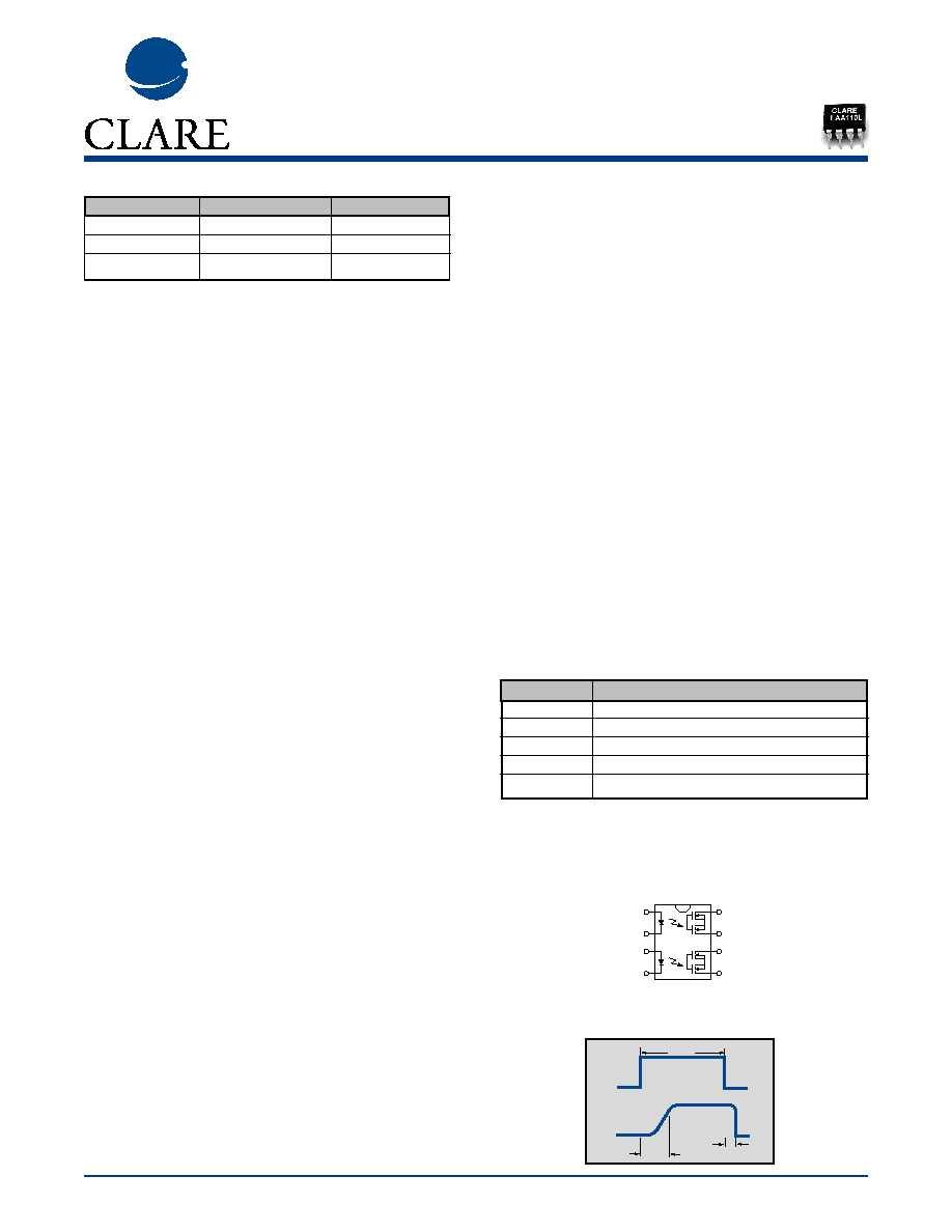
Pin Configuration
CONTROL
LOAD
10ms
10%
10%
90%
+
T
ON
T
OFF
+
+
1
2
3
4
8
7
6
5
+ Control - Switch #1
≠ Control - Switch #1
+ Control - Switch #2
≠ Control - Switch #2
Load - Switch #1
Load - Switch #1
Load - Switch #2
Load - Switch #2
AC/DC Configuration
LAA110L Pinout
Switching Charcteristics of
Normally Open (Form A) Devices

www.clare.com
2
LAA110L
Rev. 7.0
Absolute Maximum Ratings are stress ratings. Stresses in
excess of these ratings can cause permanent damage to
the device. Functional operation of the device at these or
any other conditions beyond those indicated in the opera-
tional sections of this data sheet is not implied. Exposure
of the device to the absolute maximum ratings for an
extended period may degrade the device and effect its
reliability.
Electrical Characteristics
Absolute Maximum Ratings (@ 25∞ C)
Parameter
Min
Typ
Max Units
Input Power Dissipation
-
-
150
1
mW
Input Control Current
-
-
50
mA
Peak (10ms)
-
-
1
A
Blocking Voltage
DC or AC peak
-
-
350
V
Reverse Input Voltage
-
-
5
V
Total Power Dissipation
-
-
800
2
mW
Isolation Voltage
Input to Output
3750
-
-
V
RMS
Operational Temperature
-40
-
+85
∞C
Storage Temperature
-40
-
+125
∞C
Soldering Temperature
(10 Seconds Max.)
DIP Package
-
-
+260
∞C
Flatpack/Surface Mount
Package
-
-
+220
∞C
1
Derate Linearly 1.33 mw/∞C
2
Derate Linearly 6.67 mw/∞C
Parameter
Conditions
Symbol
Min
Typ
Max
Units
Output Characteristics @ 25∞C
Load Current (Continuous)*
-
I
L
-
-
120
mA
Peak Load Current
10ms max
I
LPK
-
-
350
mA
On-Resistance
I
L
=120mA R
ON
-
30
35
Off-State Leakage Current
V
L
=350V
I
LEAK
-
-
1
µA
Switching Speeds
Turn-On
I
F
=5mA, V
L
=10V
T
ON
-
-
3
ms
Turn-Off
I
F
=5mA, V
L
=10V
T
OFF
-
-
3
ms
Output Capacitance
50V; f=1MHz
C
OUT
-
25
-
pF
Load Current Limiting
-
I
CL
130
170
210
mA
Input Characteristics @ 25∞C
Input Control Current
I
L
=120mA
I
F
5
-
50
mA
Input Dropout Current
-
-
0.4
0.7
-
mA
Input Voltage Drop
I
F
=5mA
V
F
0.9
1.2
1.4
V
Reverse Input Voltage
-
V
R
-
-
5
V
Reverse Input Current
V
R
=5V
I
R
-
-
10
µA
Input to Output Capacitance
-
C
I/O
-
3
-
pF
*Note: If both poles operate load current must be derated so as not to exceed the package power dissipation valve.
LAA110L
www.clare.com
3
Rev. 7.0
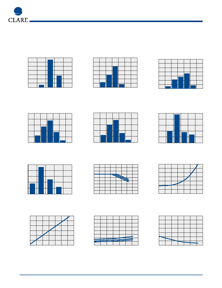
PERFORMANCE DATA*
*The Performance data shown in the graphs above is typical of device performance. For guaranteed parameters not indicated in the written specifications, please contact our application
department.
LAA110L
Typical On-Resistance Distribution
(N=50 Ambient Temperature = 25
∞C)
(Load Current = 120mADC; I
F
= 5mADC)
35
30
25
20
15
10
5
0
On-Resistance (
)
Device Count (N)
17.0
17.8
18.6
19.4
17.4
18.2
19.0
LAA110L
Typical Blocking Voltage Distribution
(N=50 Ambient Temperature = 25
∞C)
35
30
25
20
15
10
5
0
382.8
395.8
408.8
376.3
389.3
402.3
415.3
Blocking Voltage (V)
Device Count (N)
LAA110L
Typical I
F
for Switch Operation
(N=50 Ambient Temperature = 25
∞C)
(Load Current = 120mADC)
LED Current (mA)
Device Count (N)
25
20
15
10
5
0
0.75
1.35
1.95
0.45
1.05
1.65
2.25
LAA110L
Typical I
F
for Switch Dropout
(N=50 Ambient Temperature = 25
∞C)
(Load Current = 120mADC
25
20
15
10
5
0
0.75
1.35
1.95
0.45
1.05
1.65
2.25
LED Current (mA)
Device Count (N)
)
LAA110L
Typical Turn-On Time
(N=50 Ambient Temperature = 25
∞C)
(Load Current = 120mADC; I
F
= 5mADC)
0.25
0.45
0.65
0.15
0.35
0.55
Turn-On (ms)
Device Count (N)
25
20
15
10
5
0
LAA110L
Typical Blocking Voltage
vs. Temperature
Temperature (
∞C)
Blocking Voltage (V
RMS
)
-40
420
410
400
390
380
370
360
-20
0
20
40
60
80
100
LAA110L
Typical Turn-Off Time
(N=50 Ambient Temperature = 25
∞C)
(Load Current = 120mADC; I
F
= 5mADC)
0.025
0.075
0.125
0.175
0.225
Turn-Off (ms)
Device Count (N)
25
20
15
10
5
0
LAA110L
Typical Load Current vs. Temperature
Temperature (
∞C)
Load Current (mA)
180
160
140
120
100
80
60
40
20
0
-40
-20
0
20
40
60
80
120
100
20mA
10mA
5mA
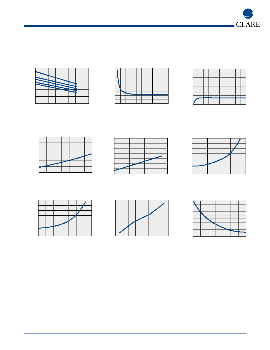
LAA110L
Typical Leakage vs. Temperature
(Measured across Pins 5 & 6 or 7 & 8)
Temperature (
∞C)
Leakage (
µ
A)
-40
0.014
0.012
0.01
0.008
0.006
0.004
0.002
0
-20
0
20
40
60
80
100
LAA110L
Typical Turn-On vs. Temperature
(Load Current = 120mADC)
Temperature (
∞C)
5mA
10mA
20mA
Turn-On (ms)
-40
1.600
1.400
1.200
1.000
0.800
0.600
0.400
0.200
0
-20
0
20
40
60
80
100
LAA110L
Typical Turn-Off vs. Temperature
(Load Current = 120mADC)
Temperature (
∞C)
Turn-Off (ms)
-40
0.700
0.600
0.500
0.400
0.300
0.200
0.100
0
-20
0
20
40
60
80
100
5mA
LAA110L
Typical LED Forward Voltage Drop
(N=50 Ambient Temperature = 25
∞C)
I
F
= 5mADC
35
30
25
20
15
10
5
0
1.17
1.19
1.21
1.23
1.25
LED Forward Voltage Drop (V)
Device Count (N)
www.clare.com
4
LAA110L
Rev. 7.0
PERFORMANCE DATA*
*The Performance data shown in the graphs above is typical of device performance. For guaranteed parameters not indicated in the written specifications, please contact our application
department.
LAA110L
Typical Turn-On vs. LED Forward Current
(Load Current = 120mADC)
LED Forward Current (mA)
Turn-On (ms)
0
5
10
15
20
25
30
35
40
45
0.9
0.8
0.7
0.6
0.5
0.4
0.3
0.2
0.1
0
50
LAA110L
Typical Turn-Off vs. LED Forward Current
(Load Current = 120mADC)
LED Forward Current (mA)
Turn-Off (ms)
0
5
10
15
20
25
30
35
40
45
0.40
0.35
0.30
0.25
0.20
0.15
0.10
0.05
0
50
LAA110L
Typical On-Resistance vs. Temperature
(Load Current = 120mADC; I
F
= 5mADC)
Temperature (
∞C)
On-Resistance (
)
-40
60.000
50.000
40.000
30.000
20.000
10.000
0
-20
0
20
40
60
80
100
LAA110L
Typical On-Resistance vs. Temperature
(Load current = 50mADC Instantaneous)
(I
F
= 5mADC)
Temperature (
∞C)
On-Resistance (
)
-40
60
50
40
30
20
10
-20
0
20
40
60
80
100
LAA110L
Typical I
F
for Switch Operation
vs. Temperature
(Load Current = 120mADC)
Temperature (
∞C)
Current (mA)
-40
3.500
3.000
2.500
2.000
1.500
1.000
0.500
0
-20
0
20
40
60
80
100
LAA110L
Typical I
F
for Switch Dropout
vs. Temperature
(Load Current = 120mADC)
Temperature (
∞C)
LED Current (mA)
-40
3.500
3.000
2.500
2.000
1.500
1.000
0.500
0
-20
0
20
40
60
80
100
LAA110L
Typical Load Current vs. Load Voltage
(Ambient Temperature = 25
∞C)
I
F
= 5mADC
Load Voltage (V)
Load Current (mA)
150
100
50
0
-50
-100
-150
-4
-3
-2
-1
0
1
2
3
4
LAA110L
Energy Rating Curve
Time
Load Current (A)
1.0
0.9
0.8
0.7
0.6
0.5
0.4
0.3
0.2
0.1
0
10
µs
1ms
100ms
10s
100
µs
10ms
1s
100s
LAA110L
Typical LED Forward Voltage Drop
vs. Temperature
Temperature (
∞C)
LED Forward Voltage Drop (V)
1.8
1.6
1.4
1.2
1.0
0.8
-40
-20
0
20
40
60
80
120
100
50mA
30mA
20mA
10mA
5mA

LAA110L
www.clare.com
5
Rev. 7.0
Dimensions
mm
(inches)
MECHANICAL DIMENSIONS
PC Board Pattern
(Top View)
6.350
± .127
(.250
± .005)
2.540
± .127
(.100
± .005)
7.620
± .127
(.300
± .005)
7.620
± .127
(.300
± .005)
8-.800 DIA.
(8-.031 DIA.)
7.239 TYP.
(.285)
3.302
(.130)
7.620
± .254
(.300
± .010)
9.144 TYP.
(.360)
6.350
± .127
(.250
± .005)
9.652
± .381
(.380
± .015)
2.540
± .127
(.100
± .005)
9.144
± .508
(.360
± .020)
.457
± .076
(.018
± .003)
8.077
± .127
(.318
± .005 )
8 Pin DIP Through Hole (Standard)
PC Board Pattern
(Top View)
2.540
± .127
(.100
± .005)
8.763
± .127
(.345
± .005)
1.193
(.047)
.787
(.031)
8 Pin Flatpack ("P" Suffix)
7.620
± .254
(.300
± .010)
2.159 TYP.
(.085)
2.286 MAX.
(.090)
9.398
± .127
(.370
± .005)
6.350
± .127
(.250
± .005)
9.652
± .381
(.380
± .015)
2.540
± .127
(.100
± .005)
8.077
± .127
(.318
± .005)
.457
± .076
(.018
± .003)
.203
(.008)
.635
± .127
(.025)
4.445
± .127
(.175
± .005)
3.302
(.130)
7.620
± .254
(.300
± .010)
6.350
± .127
(.250
± .005)
8.077
± .127
(.318
± .005)
2.540
± .127
(.100
± .005)
9.525
± .254
(.375
± .010)
.457
± .076
(.018
± .003)
.254 TYP.
(.010)
.635 TYP.
(.025)
8 Pin DIP Surface Mount ("S" Suffix)
9.652
± .381
(.380
± .015)
PC Board Pattern
(Top View)
2.540
± .127
(.100
± .005)
8.305
± .127
(.327
± .005)
1.905
± .127
(.075
± .005)
1.498
± .127
(.059
± .005)