 | –≠–ª–µ–∫—Ç—Ä–æ–Ω–Ω—ã–π –∫–æ–º–ø–æ–Ω–µ–Ω—Ç: LBB126PTR | –°–∫–∞—á–∞—Ç—å:  PDF PDF  ZIP ZIP |
1
www.clare.com
LBB126
DS-LBB126-R3
LBB126 is a 250V, 170mA, 15
2-Form-B relay. It fea-
tures lower on-resistance combined with enhanced peak
load current handling capability.
∑
Telecommunications
∑
Telecom Switching
∑
Tip/Ring Circuits
∑
Modem Switching (Laptop, Notebook, Pocket Size)
∑
Hookswitch
∑
Dial Pulsing
∑
Ground Start
∑
Ringer Injection
∑
Instrumentation
∑
Multiplexers
∑
Data Acquisition
∑
Electronic Switching
∑
I/O Subsystems
∑
Meters (Watt-Hour, Water, Gas)
∑
Medical Equipment--Patient/Equipment Isolation
∑
Security
∑
Aerospace
∑
Industrial Controls
∑
Small 8 Pin DIP Package
∑
Low Drive Power Requirements (TTL/CMOS
Compatible)
∑
No Moving Parts
∑
High Reliability
∑
Arc-Free With No Snubbing Circuits
∑
3750V
RMS
Input/Output Isolation
∑
FCC Compatible
∑
VDE Compatible
∑
No EMI/RFI Generation
∑
Machine Insertable, Wave Solderable
∑
Surface Mount and Tape & Reel Versions Available
Applications
Features
Description
DUAL POLE OptoMOS
Æ
Relay
Ordering Information
Part #
Description
LBB126
8 Pin DIP (50/Tube)
LBB126P
8 Pin Flatpack (50/Tube)
LBB126PTR
8 Pin Flatpack (1000/Reel)
LBB126S
8 Pin Surface Mount (50/Tube)
LBB126STR
8 Pin Surface Mount (1000/Reel)
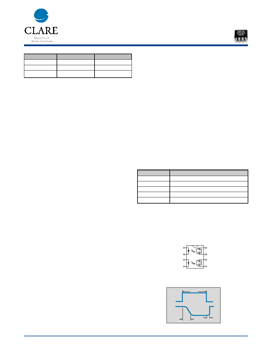
Pin Configuration
LBB126
Units
Load Voltage
250
V
Load Current
170
mA
Max R
ON
15
∑
UL Recognized: File Number E76270
∑
CSA Certified: File Number LR 43639-10
∑
BSI Certified to:
∑
BS EN 60950:1992 (BS7002:1992)
Certificate #: 7344
∑
BS EN 41003:1993
Certificate #: 7344
Approvals
Switching Characteristics of
Normally Closed (Form B) Devices
CONTROL
10ms
10%
90%
90%
+
+
T
ON
T
OFF
+
1
2
3
4
8
7
6
5
+ Control - Switch #1
≠ Control - Switch #1
+ Control - Switch #2
≠ Control - Switch #2
Load - Switch #1
AC/DC Configuration
Load - Switch #1
Load - Switch #2
Load - Switch #2
LBB126 Pinout

www.clare.com
LBB126
Rev. 3
Absolute Maximum Ratings are stress ratings. Stresses
in excess of these ratings can cause permanent damage
to the device. Functional operation of the device at these
or any other conditions beyond those indicated in the
operational sections of this data sheet is not implied.
Exposure of the device to the absolute maximum ratings
for an extended period may degrade the device and effect
its reliability.
Absolute Maximum Ratings (@ 25∞ C)
2
Parameter
Min
Typ
Max Units
Input Power Dissipation
-
-
150
1
mW
Input Control Current
-
-
50
mA
Peak (10ms)
-
-
1
A
Reverse Input Voltage
-
-
5
V
Total Power Dissipation
-
-
800
2
mW
Isolation Voltage
Input to Output
3750
-
-
V
RMS
Operational Temperature
-40
-
+85
∞C
Storage Temperature
-40
-
+125
∞C
Soldering Temperature
DIP Package
-
-
+260
∞C
Flatpack/Surface Mount
Package
-
-
+220
∞C
(10 Seconds Max.)
1
Derate Linearly 1.33 mw/∞C
2
Derate Linearly 6.67 mw/∞C
Electrical Characteristics
PARAMETER
CONDITIONS
SYMBOL
MIN
TYP
MAX
UNITS
Output Characteristics @ 25∞C
Load Voltage (Peak)
-
V
L
-
-
250
V
Load Current* (Continuous)
AC/DC Configuration
-
I
L
-
-
170
mA
Peak Load Current
10ms
I
LPK
-
-
400
mA
On-Resistance
AC/DC Configuration
I
L
=170mA
R
ON
-
10
15
Off-State Leakage Current
V
L
=350V
I
LEAK
-
-
1
µA
Switching Speeds
Turn-On
I
F
=5mA,V
L
=10V
T
ON
-
-
5
ms
Turn-Off
I
F
=5mA,V
L
=10V
T
OFF
-
-
5
ms
Output Capacitance
50V; f=1MHz
C
OUT
-
50
-
pF
Input Characteristics @ 25∞C
Input Control Current
I
L
=170mA
I
F
5
-
50
mA
Input Dropout Current
-
I
F
0.4
0.7
-
mA
Input Voltage Drop
I
F
=5mA
V
F
0.9
1.2
1.4
V
Reverse Input Voltage
-
V
R
-
-
5
V
Reverse Input Current
V
R
=5V
I
R
-
-
10
µA
Common Characteristics @ 25∞C
Input to Output Capacitance
-
C
I/O
-
3
-
pF
Input to Output Isolation
-
V
I/O
3750
-
-
V
RMS
*Note: If both poles operate simulataneously load current must be derated so as not to exceed the package power dissipation value.
LBB126
www.clare.com
Rev. 3
3
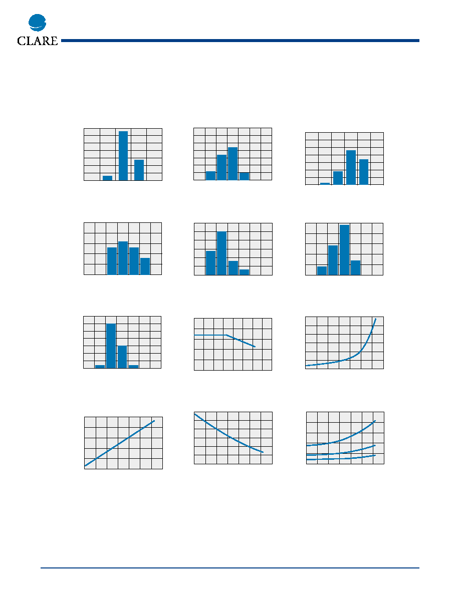
PERFORMANCE DATA*
*The Performance data shown in the graphs above is typical of device performance. For guaranteed parameters not indicated in the written specifications, please contact
our application department.
LBB126
Typical LED Forward Voltage Drop
(N=50 Ambient Temperature = 25
∞
C)
I
F
= 5mADC
35
30
25
20
15
10
5
0
1.17
1.19
1.21
1.23
1.25
LED Forward Voltage Drop (V)
Device Count (N)
LBB126
Typical On-Resistance Distribution
(N=50 Ambient Temperature = 25
∞
C)
(Load Current = 170mADC)
35
30
25
20
15
10
5
0
10.4
11.2
12.0
12.8
10.8
11.6
12.4
On-Resistance (
)
Device Count (N)
LBB126
Typical Blocking Voltage Distribution
(N=50 Ambient Temperature = 25
∞
C)
I
F
=5mADC
35
30
25
20
15
10
5
0
291.25
296.25
301.25
293.75
298.75
303.75
Device Count (N)
LBB126
Typical I
F
for Switch Dropout
(N=50 Ambient Temperature = 25
∞
C)
(Load Current = 170mADC
30
25
20
15
10
5
0
0.63
0.99
1.35
0.45
0.81
1.17
1.53
LED Current (mA)
Device Count (N)
)
LBB126
Typical I
F
for Switch Operation
(N=50 Ambient Temperature = 25
∞
C)
(Load Current = 170mADC)
0.63
0.99
1.35
0.45
0.81
1.17
1.53
LED Current (mA)
Device Count (N)
25
20
15
10
5
0
LBB126
Typical Turn-On Time
(N=50 Ambient Temperature = 25
∞
C)
(Load Current = 170mADC; I
F
= 5mADC)
0.30
0.54
0.78
1.02
0.90
0.66
0.42
Turn-On (ms)
Device Count (N)
25
20
15
10
5
0
LBB126
Typical Turn-Off Time
(N=50 Ambient Temperature = 25
∞
C)
(Load Current = 170mADC; I
F
= 5mADC)
0.625
1.125
1.625
2.125
0.875
1.375
1.875
Turn-Off (ms)
Device Count (N)
35
30
25
20
15
10
5
0
LBB126
Typical Load Current vs. Temperature
Temperature (
∞
C)
Load Current (mA)
250
200
150
100
50
0
-40 -20
0
20
40
60
80
120
100
LBB126
Typical Leakage vs. Temperature
(Measured across Pins 5 & 6 or 7 & 8)
Temperature (
∞
C)
Leakage (
µ
A)
-40
0.030
0.025
0.020
0.015
0.010
0.005
0
-20
0
20
40
60
80
100
LBB126
Typical Blocking Voltage vs. Temperature
I
F
= 5mADC
Blocking Voltage (V
RMS
)
-40
310
305
300
295
290
285
-20
0
20
40
60
80
100
LBB126
Typical Turn-On vs. Temperature
(Load Current = 170mADC)
Temperature (
∞
C)
Turn-On (ms)
-40
1.2
1.0
0.8
0.6
0.4
0.2
0
-20
0
20
40
60
80
100
5mA
LBB126
Typical Turn-Off vs. Temperature
(Load Current = 170mADC)
Temperature (
∞
C)
Turn-Off (ms)
-40
2.5
2.0
1.5
1.0
0.5
0
-20
0
20
40
60
80
100
5mA
10mA
20mA
www.clare.com
4
LBB126
Rev. 3
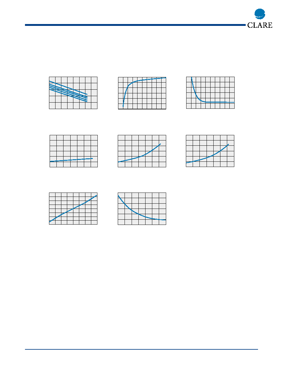
PERFORMANCE DATA*
*The Performance data shown in the graphs above is typical of device performance. For guaranteed parameters not indicated in the written specifications, please contact
our application department.
LBB126
Typical LED Forward Voltage Drop
vs. Temperature
Temperature (
∞
C)
LED Forward Voltage Drop (V)
1.8
1.6
1.4
1.2
1.0
0.8
-40
-20
0
20
40
60
80
120
100
50mA
30mA
20mA
10mA
5mA
LBB126
Typical Turn-On vs. LED Forward Current
(Load Current = 170mADC)
LED Forward Current (mA)
Turn-On (ms)
0
5
10
15
20
25
30
35
40
45
0.634
0.632
0.630
0.628
0.626
0.624
0.622
50
LBB126
Typical Turn-Off vs. LED Forward Current
(Load Current = 170mADC)
LED Forward Current (mA)
Turn-Off (ms)
0
5
10
15
20
25
30
35
40
45
1.2
1.0
0.8
0.6
0.4
0.2
0
50
LBB126
Typical On-Resistance vs. Temperature
(Load Current = 170mADC)
Temperature (
∞
C)
On-Resistance (
)
-40
60
50
40
30
20
10
0
-20
0
20
40
60
80
100
LBB126
Typical I
F
for Switch Operation
vs. Temperature
(Load Current = 170mADC)
Temperature (
∞
C)
LED Current (mA)
-40
3.000
2.500
2.000
1.500
1.000
0.500
0
-20
0
20
40
60
80
100
LBB126
Typical I
F
for Switch Dropout
vs. Temperature
(Load Current = 170mADC)
Temperature (
∞
C)
LED Current (mA)
-40
3.000
2.500
2.000
1.500
1.000
0.500
0
-20
0
20
40
60
80
100
LBB126
Typical Load Current vs. Load Voltage
(Ambient Temperature = 25
∞
C)
Load Voltage (V)
Load Current (mA)
200
150
100
50
0
-50
-100
-150
-200
-2.0
-1.5
-0.5
-1.0
0
0.5
1.5
1.0
2.0
LBB126
Energy Rating Curve
Time
Load Current (A)
10
µ
s
1.2
1.0
0.8
0.6
0.4
0.2
0
1ms
100
µ
s
100ms
1s
10ms
10s
100s
LBB126
www.clare.com
5
Rev. 3
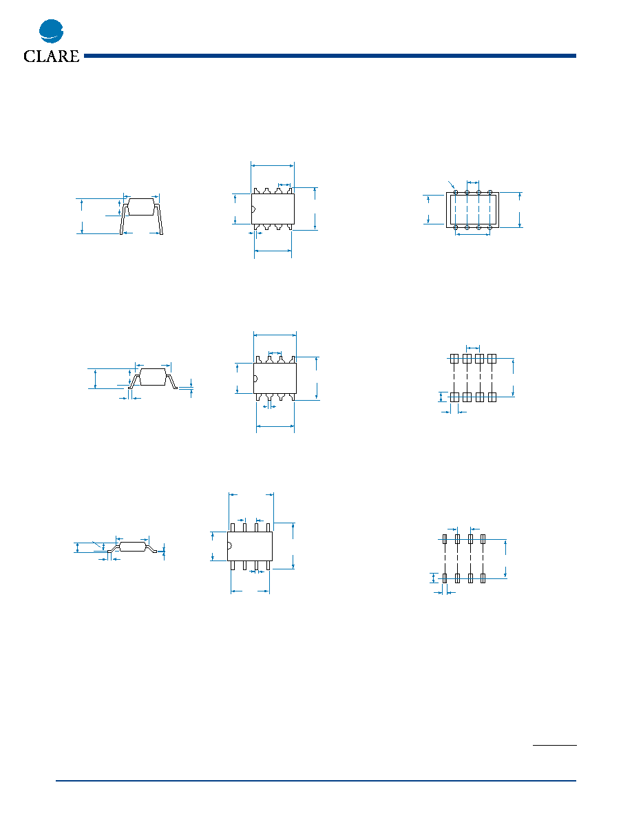
Dimensions
mm
(inches)
Mechanical Dimensions
4.445
±
.127
(.175
±
.005)
3.302
(.130)
7.620
±
.254
(.300
±
.010)
6.350
±
.127
(.250
±
.005)
8.077
±
.127
(.318
±
.005)
2.540
±
.127
(.100
±
.005)
9.525
±
.254
(.375
±
.010)
.457
±
.076
(.018
±
.003)
.254 TYP.
(.010)
.635 TYP.
(.025)
8 Pin DIP Surface Mount ("S" Suffix)
9.652
±
.381
(.380
±
.015)
PC Board Pattern
(Top View)
6.350
±
.127
(.250
±
.005)
2.540
±
.127
(.100
±
.005)
7.620
±
.127
(.300
±
.005)
7.620
±
.127
(.300
±
.005)
8-.800 DIA.
(8-.031 DIA.)
7.239 TYP.
(.285)
3.302
(.130)
7.620
±
.254
(.300
±
.010)
9.144 TYP.
(.360)
6.350
±
.127
(.250
±
.005)
9.652
±
.381
(.380
±
.015)
2.540
±
.127
(.100
±
.005)
9.144
±
.508
(.360
±
.020)
.457
±
.076
(.018
±
.003)
8.077
±
.127
(.318
±
.005 )
8 Pin DIP Through Hole (Standard)
PC Board Pattern
(Top View)
2.540
±
.127
(.100
±
.005)
8.305
±
.127
(.327
±
.005)
1.905
±
.127
(.075
±
.005)
1.498
±
.127
(.059
±
.005)
PC Board Pattern
(Top View)
2.540
±
.127
(.100
±
.005)
8.763
±
.127
(.345
±
.005)
1.193
(.047)
.787
(.031)
8 Pin Flatpack ("P" Suffix)
7.620
±
.254
(.300
±
.010)
2.159 TYP.
(.085)
2.286 MAX.
(.090)
9.398
±
.127
(.370
±
.005)
6.350
±
.127
(.250
±
.005)
9.652
±
.381
(.380
±
.015)
2.540
±
.127
(.100
±
.005)
8.077
±
.127
(.318
±
.005)
.457
±
.076
(.018
±
.003)
.203
(.008)
.635
±
.127
(.025)
www.clare.com
6
LBB126
Rev. 3
Dimensions
mm
(inches)
Mechanical Dimensions
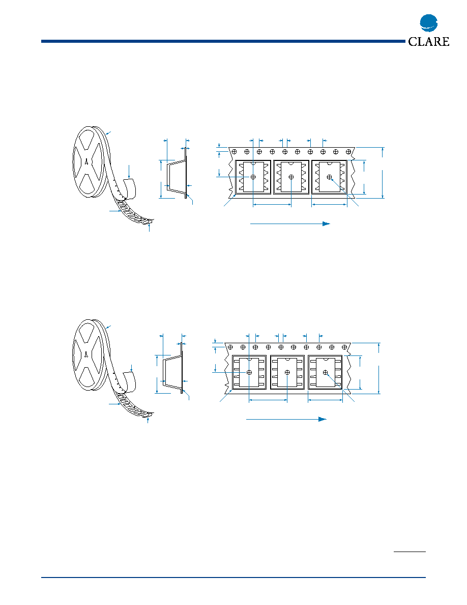
Tape and Reel Packaging for 8 Pin Flatpack Package
7.493
±
.102
(.295
±
.004)
12.090
(.476)
1.753
±
0.102
(.069
±
.004)
3.987
±
.102
(.157
±
.004)
1.498
±
.102
(.059
±
.004)
6.731 MAX.
(.265)
.406 MAX.
(.016)
4.877
(.192)
Top Cover
Tape
2.007
±
.102
(.079
±
.004)
11.988
±
.102
(.472
±
.004)
User Direction of Feed
.050R TYP.
16.002
±
.305
(.630
±
.012)
10.287
(.405)
Embossment
Embossed Carrier
Top Cover
Tape Thickness
.102 MAX.
(.004)
10.287
±
.102
(.405
±
.004)
1.549
±
.102
(.061
±
.004)
330.2 DIA.
(13.00)
1
8
Tape and Reel Packaging for 8 Pin Surface Mount Package
7.493
±
.102
(.295
±
.004)
12.090
(.476)
1.753
±
.102
(.069
±
.004)
3.987
±
.102
(.157
±
.004)
1.498
±
.102
(.059
±
.004)
6.731 MAX.
(.265)
.406 MAX.
(.016)
4.877
(.192)
Top Cover
Tape
2.007
±
.102
(.079
±
.004)
11.989
±
.102
(.472
±
.004)
User Direction of Feed
.050R TYP.
16.002
±
.305
(.630
±
.012)
10.300
(.405)
Embossment
Embossed Carrier
Top Cover
Tape Thickness
.102 MAX.
(.004)
10.300
±
.102
(.405
±
.004)
1.549
±
.102
(.061
±
.004)
330.2 DIA.
(13.00)
1
8

CLARE LOCATIONS
Clare Headquarters
78 Cherry Hill Drive
Beverly, MA 01915
Tel: 1-978-524-6700
Fax: 1-978-524-4900
Toll Free: 1-800-27-CLARE
Clare Micronix Division
145 Columbia
Aliso Viejo, CA 92656-1490
Tel: 1-949-831-4622
Fax: 1-949-831-4628
SALES OFFICES
AMERICAS
Americas Headquarters
Clare
78 Cherry Hill Drive
Beverly, MA 01915
Tel: 1-978-524-6700
Fax: 1-978-524-4900
Toll Free: 1-800-27-CLARE
Eastern Region
Clare
P.O. Box 856
Mahwah, NJ 07430
Tel: 1-201-236-0101
Fax: 1-201-236-8685
Toll Free: 1-800-27-CLARE
Central Region
Clare Canada Ltd.
3425 Harvester Road, Suite 202
Burlington, Ontario L7N 3N1
Tel: 1-905-333-9066
Fax: 1-905-333-1824
Western Region
Clare
1852 West 11th Street, #348
Tracy, CA 95376
Tel: 1-209-832-4367
Fax: 1-209-832-4732
Toll Free: 1-800-27-CLARE
Canada
Clare Canada Ltd.
3425 Harvester Road, Suite 202
Burlington, Ontario L7N 3N1
Tel: 1-905-333-9066
Fax: 1-905-333-1824
EUROPE
European Headquarters
CP Clare nv
Bampslaan 17
B-3500 Hasselt (Belgium)
Tel: 32-11-300868
Fax: 32-11-300890
France
Clare France Sales
Lead Rep
99 route de Versailles
91160 Champlan
France
Tel: 33 1 69 79 93 50
Fax: 33 1 69 79 93 59
Germany
Clare Germany Sales
ActiveComp Electronic GmbH
Mitterstrasse 12
85077 Manching
Germany
Tel: 49 8459 3214 10
Fax: 49 8459 3214 29
Italy
C.L.A.R.E.s.a.s.
Via C. Colombo 10/A
I-20066 Melzo (Milano)
Tel: 39-02-95737160
Fax: 39-02-95738829
Sweden
Clare Sales
Comptronic AB
Box 167
S-16329 SpÂnga
Tel: 46-862-10370
Fax: 46-862-10371
United Kingdom
Clare UK Sales
Marco Polo House
Cook Way
Bindon Road
Taunton
UK-Somerset TA2 6BG
Tel: 44-1-823 352541
Fax: 44-1-823 352797
ASIA/PACIFIC
Asian Headquarters
Clare
Room N1016, Chia-Hsin,
Bldg II, 10F, No. 96, Sec. 2
Chung Shan North Road
Taipei, Taiwan R.O.C.
Tel: 886-2-2523-6368
Fax: 886-2-2523-6369
http://www.clare.com
Worldwide Sales Offices
Specification: DS-LBB126-R3
©Copyright 2000, Clare, Inc.
OptoMOS
Æ
is a registered trademark of Clare, Inc.
All rights reserved. Printed in USA.
2/23/01
Clare cannot assume responsibility for use of any circuitry other
than circuitry entirely embodied in this Clare product. No circuit
patent licenses nor indemnity are expressed or implied. Clare
reserves the right to change the specification and circuitry, with-
out notice at any time. The products described in this document
are not intended for use in medical implantation or other direct life
support applications where malfunction may result in direct phys-
ical harm, injury or death to a person.