 | –≠–ª–µ–∫—Ç—Ä–æ–Ω–Ω—ã–π –∫–æ–º–ø–æ–Ω–µ–Ω—Ç: LCA100STR | –°–∫–∞—á–∞—Ç—å:  PDF PDF  ZIP ZIP |
1
www.clare.com
LCA100
DS-LCA100-R1
LCA100 is a 350V, 120mA, 25
1-Form-A relay. It fea-
tures the lowest on-resistance in an OptoMOS relay with
350V peak load voltage. Current limiting version is also
available. ("L" suffix)
∑
Telecommunications
∑
Telecom Switching
∑
Tip/Ring Circuits
∑
Modem Switching (Laptop, Notebook, Pocket Size)
∑
Hookswitch
∑
Dial Pulsing
∑
Ground Start
∑
Ringer Injection
∑
Instrumentation
∑
Multiplexers
∑
Data Acquisition
∑
Electronic Switching
∑
I/O Subsystems
∑
Meters (Watt-Hour, Water, Gas)
∑
Medical Equipment--Patient/Equipment Isolation
∑
Security
∑
Aerospace
∑
Industrial Controls
∑
UL Recognized: File Number E76270
∑
CSA Certified: File Number LR 43639-10
∑
BSI Certified to:
∑
BS EN 60950:1992 (BS7002:1992)
Certificate #: 7344
∑
BS EN 41003:1993
Certificate #: 7344
∑
Small 6 Pin DIP Package
∑
Low Drive Power Requirements (TTL/CMOS
Compatible)
∑
No Moving Parts
∑
High Reliability
∑
Arc-Free With No Snubbing Circuits
∑
3750V
RMS
Input/Output Isolation
∑
FCC Compatible
∑
VDE Compatible
∑
No EMI/RFI Generation
∑
Machine Insertable, Wave Solderable
∑
Surface Mount and Tape & Reel
Versions Available
Applications
Features
Description
Approvals
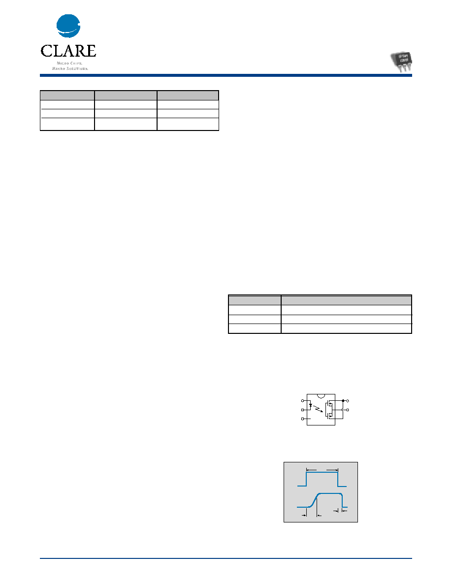
Single Pole OptoMOS
Æ
Relay
Ordering Information
Part #
Description
LCA100
6 Pin DIP (50/Tube)
LCA100S
6 Pin Surface Mount (50/Tube)
LCA100STR
6 Pin Surface Mount (1000/Reel)
LCA100
Units
Load Voltage
350
V
Load Current
120
mA
Max R
ON
25
Pin Configuration
CONTROL
LOAD
10ms
10%
10%
90%
+
T
ON
T
OFF
+
+
Switching Characteristics of
Normally Open (Form A) Devices
1
3
2
4
5
6
+ Control
≠ Control
Do Not Use
+ Load
≠ Load
DC Only Configuration
LCA100/LCA100L Pinout
www.clare.com
LCA100
Rev. 1
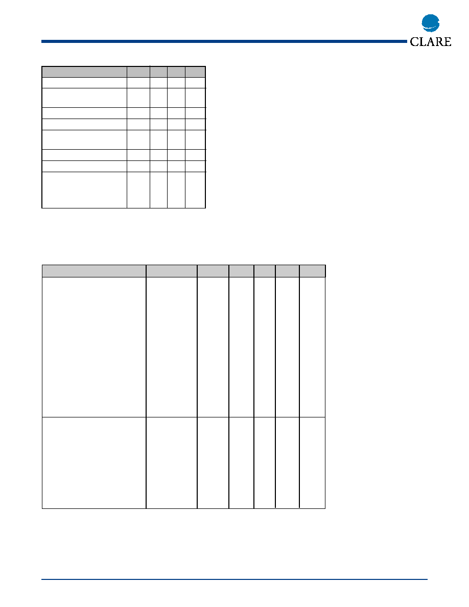
Absolute Maximum Ratings are stress ratings. Stresses
in excess of these ratings can cause permanent damage
to the device. Functional operation of the device at these
or any other conditions beyond those indicated in the
operational sections of this data sheet is not implied.
Exposure of the device to the absolute maximum ratings
for an extended period may degrade the device and effect
its reliability.
Absolute Maximum Ratings (@ 25∞ C)
2
Parameter
Min
Typ
Max Units
Input Power Dissipation
-
-
150
1
mW
Input Control Current
-
-
50
mA
Peak (10ms)
-
-
1
A
Reverse Input Voltage
-
-
5
V
Total Power Dissipation
-
-
800
2
mW
Isolation Voltage
Input to Output
3750
-
-
V
RMS
Operational Temperature
-40
-
+85
∞C
Storage Temperature
-40
-
+125
∞C
Soldering Temperature
(10 Seconds Max.)
DIP Package
-
-
+260
∞C
Surface Mount Package
-
-
+220
∞C
1
Derate Linearly 1.33 mw/∞C
2
Derate Linearly 6.67 mw/∞C
Electrical Characteristics
Parameter
Conditions
Symbol
Min
Typ
Max
Units
Output Characteristics @ 25∞C
Load Voltage (Peak)
-
V
L
-
-
350
V
Load Current (Continuous)
AC/DC Configuration
-
I
L
-
-
120
mA
DC Configuration
-
I
L
-
-
200
mA
Peak Load Current
10ms
I
LPK
-
-
350
mA
On-Resistance
AC/DC Configuration
I
L
=120mA
R
ON
-
-
25
DC Configuration
I
L
=200mA
R
ON
-
-
8
Off-State Leakage Current
V
L
=35OV
I
LEAK
-
-
1
µA
Switching Speeds
Turn-On
I
F
=5mA, V
L
=10V
T
ON
-
-
5
ms
Turn-Off
I
F
=5mA, V
L
=10V
T
OFF
-
5
ms
Output Capacitance
50V; f=1MHz
C
OUT
-
35
-
pF
Input Characteristics @ 25∞C
Input Control Current
I
L
=120mA
I
F
5
-
50
mA
Input Dropout Current
-
I
F
0.4
0.7
-
mA
Input Voltage Drop
I
F
=5mA
V
F
0.9
1.2
1.4
V
Reverse Input Voltage
-
V
R
-
-
5
V
Reverse Input Current
V
R
=5V
I
R
-
-
10
µA
Input to Output Capacitance
-
C
I/O
-
3
-
pF
Input to Output Isolation
-
V
I/O
3750
-
-
V
RMS
LCA100
Rev. 1
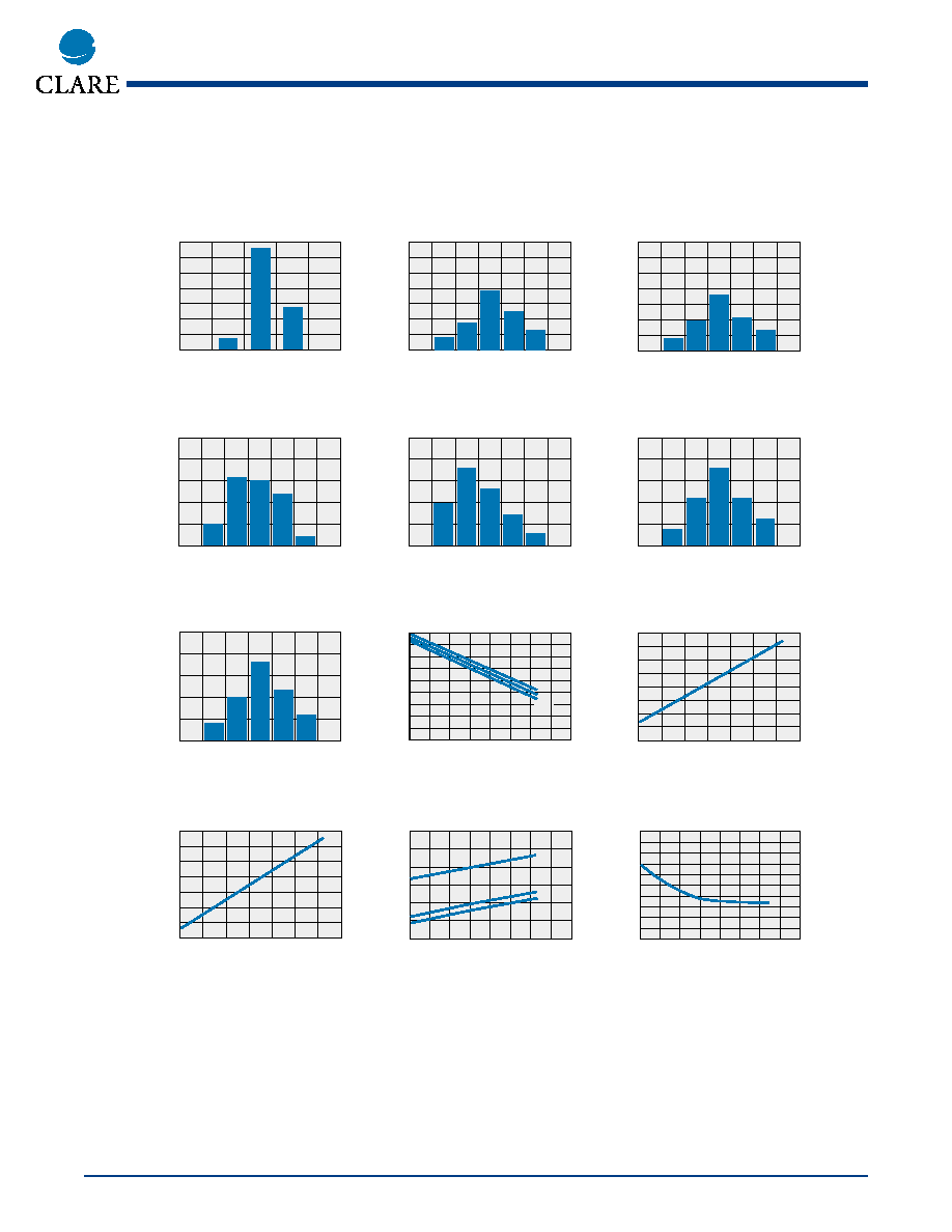
PERFORMANCE DATA*
The Performance data shown in the graphs above is typical of device performance. For guaranteed parameters not indicated in the written specifications, please contact
our application department.
3
LCA100
Typical LED Forward Voltage Drop
(N=50 Ambient Temperature = 25
∞
C)
I
F
= 5mADC
35
30
25
20
15
10
5
0
1.17
1.19
1.21
1.23
1.25
LED Forward Voltage Drop (V)
Device Count (N)
LCA100
Typical On-Resistance Distribution
(N=50 Ambient Temperature = 25
∞
C)
(Load Current = 120mADC)
35
30
25
20
15
10
5
0
13.93
14.17
14.41
14.66
14.05
14.29
14.54
On-Resistance (
)
Device Count (N)
LCA100
Typical Blocking Voltage Distribution
(N=50 Ambient Temperature = 25
∞
C)
35
30
25
20
15
10
5
0
369.8
379.4
388.9
398.4
374.6
384.1
393.7
Blocking Voltage (V)
Device Count (N)
LCA100
Typical I
F
for Switch Operation
(N=50 Ambient Temperature = 25
∞
C)
(Load Current = 120mADC)
0.90
1.00
1.10
0.85
0.95
1.05
1.15
LED Current (mA)
Device Count (N)
25
20
15
10
5
0
LCA100
Typical I
F
for Switch Dropout
(N=50 Ambient Temperature = 25
∞
C)
(Load Current = 120mADC
25
20
15
10
5
0
0.90
1.00
1.10
0.85
0.95
1.05
1.15
LED Current (mA)
Device Count (N)
)
LCA100
Typical Turn-On Time
(N=50 Ambient Temperature = 25
∞
C)
(Load Current = 120mADC; I
F
= 5mADC)
1.72
2.02
2.32
2.61
1.87
2.17
2.46
Turn-On (ms)
Device Count (N)
25
20
15
10
5
0
LCA100
Typical Turn-Off Time
(N=50 Ambient Temperature = 25
∞
C)
(Load Current = 120mADC; I
F
= 5mADC)
0.06
0.10
0.15
0.19
0.17
0.13
0.08
Turn-Off (ms)
Device Count (N)
25
20
15
10
5
0
LCA100
Typical Load Current vs. Temperature
Temperature (
∞
C)
Load Current (mA)
180
160
140
120
100
80
60
40
20
0
-40
-20
0
20
40
60
80
120
100
20mA
10mA
5mA
LCA100
Typical Leakage vs. Temperature
(Measured across Pins 4 & 6)
Temperature (
∞
C)
Leakage (
µ
A)
-40
0.016
0.014
0.012
0.010
0.008
0.006
0.004
0.002
0
-20
0
20
40
60
80
100
LCA100
Typical Blocking Voltage
vs. Temperature
Temperature (
∞
C)
Blocking Voltage (V
RMS
)
-40
410
405
400
395
390
385
380
375
-20
0
20
40
60
80
100
LCA100
Typical Turn-On vs. Temperature
(Load Current = 120mADC)
Temperature (
∞
C)
5mA
10mA
20mA
Turn-On (ms)
-40
3.000
2.500
2.000
1.500
1.000
0.500
0
-20
0
20
40
60
80
100 120
LCA100
Typical Turn-Off vs. Temperature
(Load Current = 100mADC)
Temperature (
∞
C)
Turn-Off (ms)
-40
0.50
0.45
0.40
0.35
0.30
0.25
0.20
0.15
0.10
0.05
0
-20
0
20
40
60
80
100
120
www.clare.com
www.clare.com
4
LCA100
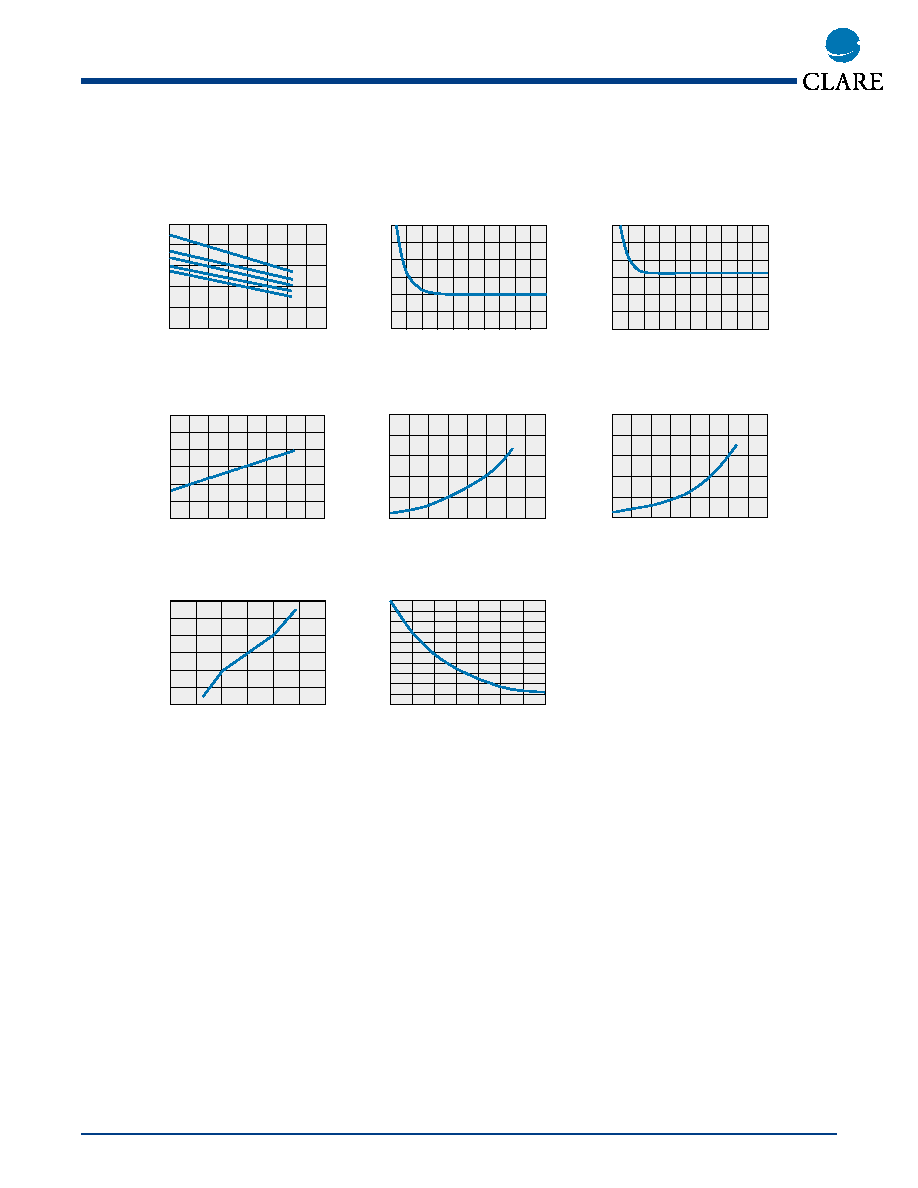
Rev. 1
LCA100
Typical LED Forward Voltage Drop
vs. Temperature
Temperature (
∞
C)
LED Forward Voltage Drop (V)
1.8
1.6
1.4
1.2
1.0
0.8
-40
-20
0
20
40
60
80
120
100
50mA
30mA
20mA
10mA
5mA
LCA100
Typical Turn-On vs. LED Forward Current
(Load Current = 120mADC)
LED Forward Current (mA)
Turn-On (ms)
0
5
10
15
20
25
30
35
40
45
3.0
2.5
2.0
1.5
1.0
0.5
0
50
LCA100
Typical Turn-Off vs. LED Forward Current
(Load Current = 120mADC)
LED Forward Current (mA)
Turn-Off (ms)
0
5
10
15
20
25
30
35
40
45
0.30
0.25
0.20
0.15
0.10
0.05
0
50
LCA100
Typical On-Resistance vs. Temperature
(Load Current = 120mADC; I
F
= 5mADC)
Temperature (
∞
C)
On-Resistance (
)
-40
30
25
20
15
10
5
0
-20
0
20
40
60
80
100 120
LCA100
Typical I
F
for Switch Operation
vs. Temperature
(Load Current = 120mADC)
Temperature (
∞
C)
LED Current (mA)
-40
5.0
4.0
3.0
2.0
1.0
0
-20
0
20
40
60
80
100
120
LCA100
Typical I
F
for Switch Dropout
vs. Temperature
(Load Current = 120mADC)
Temperature (
∞
C)
LED Current (mA)
-40
5.0
4.0
3.0
2.0
1.0
0
-20
0
20
40
60
80
100
120
LCA100
Typical Load Current vs. Load Voltage
(Ambient Temperature = 25
∞
C)
I
F
= 5mADC
Load Voltage (V)
Load Current (mA)
150
100
50
0
-50
-100
-150
-3
-2
-1
0
1
2
3
LCA100
Energy Rating Curve
Time
Load Current (A)
10
µ
s
1.0
0.9
0.8
0.7
0.6
0.5
0.4
0.3
0.2
0.1
0
1ms
100
µ
s
100ms
1s
10ms
10s
100s
PERFORMANCE DATA*
The Performance data shown in the graphs above is typical of device performance. For guaranteed parameters not indicated in the written specifications, please contact
our application department.

LCA100
www.clare.com
5
Rev. 1
Mechanical Dimensions
PC Board Pattern
(Top View)
2.540
±
.127
(.100
±
.005)
8.305
±
.127
(.327
±
.005)
1.905
±
.127
(.075
±
.005)
1.499
±
.127
(.059
±
.005)
4.445
±
.127
(.175
±
.005)
3.302
(.130)
7.620
±
.254
(.300
±
.010)
6.350
±
.127
(.250
±
.005)
8.382
±
.635
(.330
±
.025)
2.540
±
.127
(.100
±
.005)
9.525
±
.254
(.375
±
.010)
.457
±
.076
(.018
±
.003)
.254 TYP.
(.010)
.635 TYP.
(.025)
6 Pin DIP Surface Mount ("S" Suffix)
Tape and Reel Packaging for 6 Pin Surface Mount Package
7.493
±
.102
(.295
±
.004)
12.090
(.476)
330.2 DIA.
(13.00)
1.753
±
.102
(.069
±
.004)
3.987
±
.102
(.157
±
.004)
1.498
±
.102
(.059
±
.004)
6.731 MAX.
(.265)
.406 MAX.
(.016)
4.877
(.192)
Top Cover
Tape
2.007
±
.102
(.079
±
.004)
11.989
±
.102
(.472
±
.004)
User Direction of Feed
.050R TYP.
16.002
±
.305
(.630
±
.012)
10.100
(.398)
Embossment
Embossed Carrier
Top Cover
Tape Thickness
.102 MAX.
(.004)
10.100
±
.102
(.398
±
.004)
1.549
±
.102
(.061
±
.004)
1
6
Dimensions
mm
(inches)
PC Board Pattern
(Top View)
6.350
±
.127
(.250
±
.005)
2.540
±
.127
(.100
±
.005)
7.620
±
.127
(.300
±
.005)
5.080
±
.127
(.200
±
.005)
6-.800 DIA.
(6-.031 DIA.)
6.350
±
.127
(.250
±
.005)
8.382
±
.635
(.330
±
.025)
2.540
±
.127
(.100
±
.005)
9.144
(.360)
.457
±
.076
(.018
±
.003)
6 Pin DIP Through Hole (Standard)
7.239 TYP.
(.285)
3.302
(.130)
7.620
±
.254
(.300
±
.010)
9.144
±
.508
(.360
±
.020)