 | –≠–ª–µ–∫—Ç—Ä–æ–Ω–Ω—ã–π –∫–æ–º–ø–æ–Ω–µ–Ω—Ç: LIA101 | –°–∫–∞—á–∞—Ç—å:  PDF PDF  ZIP ZIP |
1
www.clare.com
LIA101
DS-LIA101-RX
The LIA100 and LIA101 are linear isolation amplifiers that
integrate a linear optocoupler with two op amps in a sin-
gle package. They are available in a 16 Pin SOIC or DIP
package.
∑
Isolated 4-20mA Converter
∑
Medical Sensor Isolation
∑
Switching Power Supply Feedback Circuits
∑
Isolated Temperature/Pressure Sensors
∑
Data Acquisition Equipment
∑
Isolated Motor Controls
∑
UL Recognized: File Number E76270
∑
CSA Certified: File Number LR 43639-10
∑
BSI Certified to:
∑
BS EN 60950:1992 (BS7002:1992)
Certificate #: 7344
∑
BS EN 41003:1993
Certificate #: 7344
∑
Small Size Standard 16 Pin SOIC or DIP Package
∑
0.01% Servo Linearity
∑
5300 VAC Peak Input/Output Isolation Available
∑
Bandwidth
40kHz
∑
Machine Insertable, Wave Solderable
∑
Wide Power Supply Range ±18V
∑
Low Supply Current
Applications
Features
Description
Approvals
Linear Isolation Amplifier
Ordering Information
Part #
Description
LIA101
16 Pin DIP (50/Tube)
LIA101P
16 Pin Flatpack (50/Tube)
LIA101PTR
16 Pin Flatpack (1000/Reel)
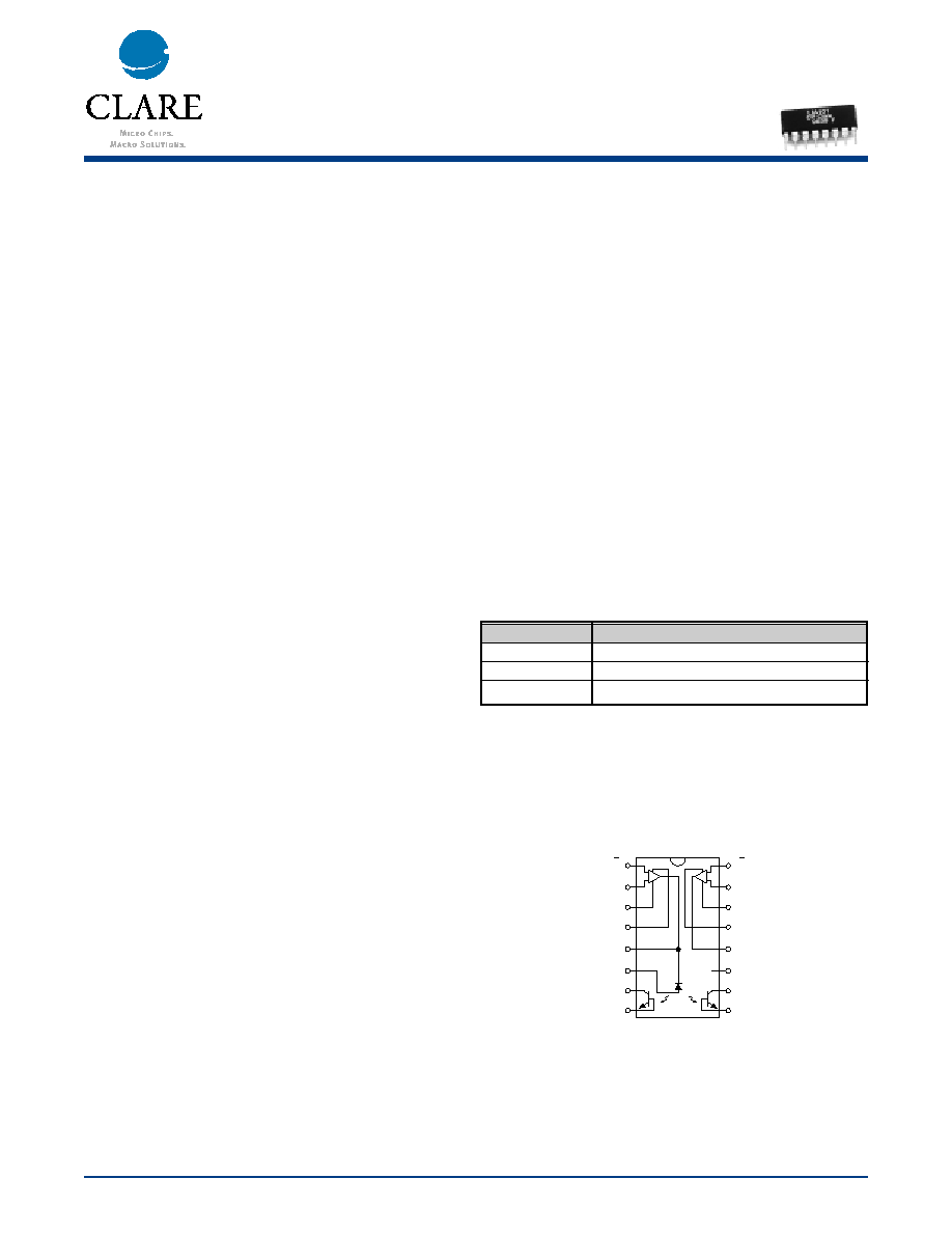
Pin Configuration
LIA100/LIA101 Pinout
+
A1 INPUT
A2 INPUT
V
EE2
V
CC2
V
CC1
V
EE1
Output
N.C.
Output (I
2
)
Comp. (to C
F
)
LED
Servo (I
1
)
+
1
2
3
4
16
15
14
13
5
6
7
8
12
11
10
9

www.clare.com
LIA101
Rev. X
Absolute Maximum Ratings are stress ratings. Stresses
in excess of these ratings can cause permanent damage
to the device. Functional operation of the device at these
or any other conditions beyond those indicated in the
operational sections of this data sheet is not implied.
Exposure of the device to the absolute maximum ratings
for an extended period may degrade the device and effect
its reliability.
Absolute Maximum Ratings (@ 25∞ C)
2
Parameter
Min
Typ
Max Units
Supply Voltages
± 5
-
±18
V
Differential Input Voltage
-
-
± 30
V
Output Short Circuit Duration
Continuous
-
Total Package Dissipation
-
-
11
W
Isolation Voltage
Input to Output
3750
-
-
V
RMS
Operational Temperature
-40
-
+85
∞C
Storage Temperature
-40
-
+125
∞C
Soldering Temperature
DIP Package
-
-
+260
∞C
Surface Mount Package
-
-
+220
∞C
(10 Seconds Max.)
1
Above 25∞C Derate Linearly 1.67mW/∞C
Electrical Characteristics @ TA = +25∞C and
±VCC = 15VDC (unless otherwise specified)
PARAMETERS
CONDITIONS
MIN
TYP
MAX
UNITS
Isolation
Continuous Voltage, AC
-
-
-
3750
V
RMS
Input to Output Leakage Current
1000V
RMS
, 60Hz
-
0.2
-
µA
RMS
Offset Voltage
Output Offset Voltage (VOS)
R
F
=R
IN
=51K
, K3=1.000
-
50
-
mV
Input Grounded T
A
=25∞C
Amplifier Input Impedance
-
-
10
12
|| 3
-
|| pF
VOS/
T Average TC of Input
Offset Voltage
R
S
=50
-
5
-
µV/∞C
(Input and Output Stage)
Common Mode Rejection Ratio, CMRR
60Hz, R
F
=1M
-
100
-
dB
R
IN
=10K
, Gain=100
Input Offset Voltage
R
S
=50
, T
A
=25∞C
-
3
10
mV
Common Mode Range
±12
-
-
V
Frequency Response
Bandwidth
-
-
40
-
kHz
Slew Rate
0-10V Step Input
-
0.3
-
V/µs
Non-Linearity
F
O
=300Hz, -10dBm
-
-
0.01
%
Power Supplies
Input Stage Supply Voltage VCC1, VEE1
-
±5
-
±18
V
Output Stage Supply Voltage VCC2, VEE2
-
±5
-
±18
V
Input (A1) & Output Stage (A2) Supply Current
-
-
5
10
mA
Power Supply Rejection Ratio, PSRR
-
-
80
100
dB
LIA101
www.clare.com
3
Rev. X
PARAMETERS
CONDITIONS
MIN
TYP
MAX
UNITS
LED Parameters
Forward LED Current (IF)
-
-
-
20
mA
LED Forward Voltage Drop (VF)
I
F
=10mA
0.9
1.2
1.4
V
Reverse LED Current
V
R
=5V
-
-
10
µA
Reverse LED Voltage
-
-
-
5
V
Coupled Characteristics
K1, Servo Gain (I1/IF)
I
F
=2-10mA, V
CC
=15V
0.004
0.008
0.030
K2, Forward Gain (I2/IF)
I
F
=2-10mA, V
CC
=15V
0.004
0.008
0.030
K3, Transfer Gain (K2/K1)
I
F
=2-10mA, V
CC
=15V
0.733
1.000
1.072
K3, Temperature Coefficient
Over Temperature Range
-
0.005
-
%/∞C
Temperature Range
Operating
-
-40
-
+85
∞C
Storage
-
-40
-
+125
∞C
Electrical Characteristics @ TA = +25∞C and
±VCC = 15VDC (unless otherwise specified) (Continued)
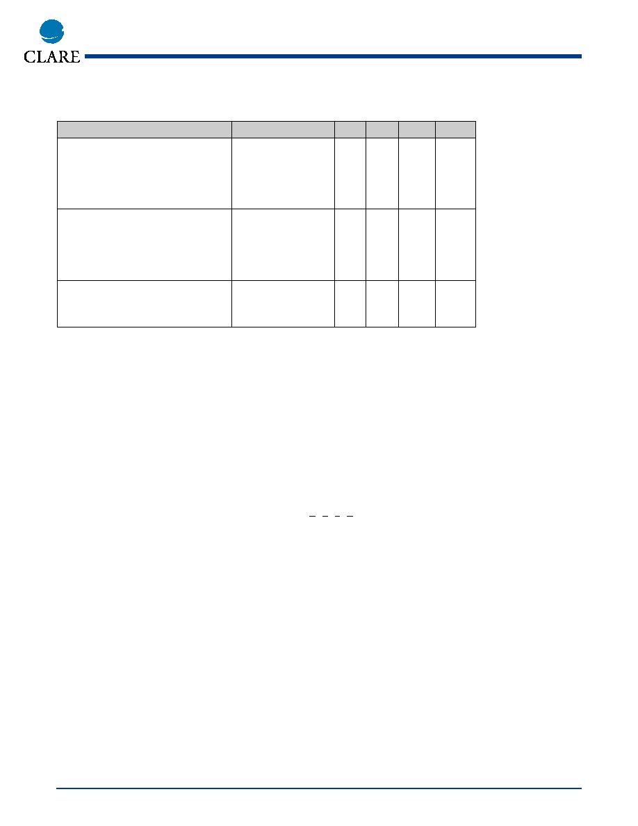
s
The LIA101 Series (through hole) is shipped in anti-static tubes of 25 pieces. The LIA100P Series
(flatpack) is shipped in anti-static tubes of 50 pieces. Each tube will contain one K3 sorted bin.
s
Bin designation marked on each device (A-J).
s
Orders for the LIA100/LIA100P product will be shipped using bins available at the date of the order.
Any bin (A-J) can be shipped.
s
For customers requiring selected bins D E F G we offer part numbers LIA101/LIA101P.
K3 Sorted Bins
Bin A
= 0.550-0.605
Bin B
= 0.606-0.667
Bin C
= 0.668-0.732
Bin D
= 0.733-0.805
Bin E
= 0.806-0.886
Bin F
= 0.887-0.974
Bin G
= 0.975-1.072
Bin H
= 1.073-1.179
Bin I
= 1.180-1.297
Bin J
= 1.298-1.426
4
LIA101
Rev. X
www.clare.com
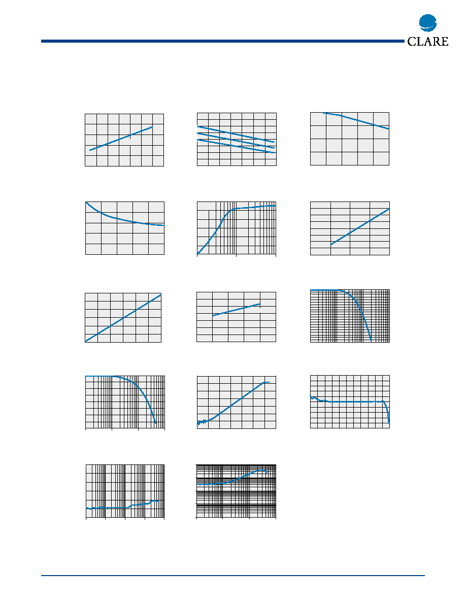
PERFORMANCE DATA*
The Performance data shown in the graphs above is typical of device performance. For guaranteed parameters not indicated in the written specifications, please contact
our application department.
LIA100/LIA101
LED Peak Wavelength vs.
Ambient Temperature
900
890
880
870
860
850
-50
-25
0
25
50
75
100
125
Temperature (
∞
C)
Shift in Wavelength - nm
875nm @ 25
∞
C
LIA100/LIA101
Typical LED Forward Voltage Drop
vs. LED Temperature
1.7
1.6
1.5
1.4
1.3
1.2
1.1
1.0
-40
-20
0
20
40
60
80
100
Temperature (
∞
C)
LED Forward Voltage Drop (V)
20mA
10mA
5mA
LIA100/LIA101
LED Power vs. Time @
Die Temperature of 70
∞
C
0
20000
40000
60000
80000
100000
100
Time (Hours)
LED Power (%)
95
90
85
80
LIA100/LIA101
LED Power vs. Time @
Die Temperature of 150
∞
C
0
20000
40000
60000
80000
100000
100
80
60
40
20
0
Time (Hours)
LED Power (%)
Peak to Peak Output
Swing (V)
0.1
1
10
28
24
20
16
12
8
4
Output Load R
L
(K
)
LIA100/LIA101
Op-Amp Output Voltage
Swing vs. R
L
V
S
=
±
15V
T
A
= 25
∞
C
20
40
35
30
25
20
15
10
5
0
5
10
15
Supply Voltage (
±
V)
Peak to Peak Output
Swing (V)
LIA100/LIA101
Op-amp Output Voltage Swing
vs. Supply Voltage
T
A
= 25
∞
C
R
L
= 2K
0
LIA100/LIA101
Input / Output Leakage Current vs.
RMS Voltage
800
700
600
500
400
300
200
1
1.5
2
2.5
3
3.5
4
RMS Voltage (kV)
Input/Output
Leakage Current (nA)
LIA100/LIA101
Individual Op-Amp Supply Current vs.
Supply Voltage
7
6
5
4
3
2
1
0
0
5
10
15
20
25
Supply Voltage (V)
Supply Current (mA)
T
C
= 25
∞
C
0
-2
-4
-6
-8
-10
-12
-14
-16
-18
-20
1
10
100
1000
Frequency (kHz)
Amplitude (dB)
LIA100/LIA101
Frequency Response
(R
F
= R
IN
= 20k
, C
F
= 20pF) TA = 25
∞
C
100
0
-10
-20
-30
-40
-50
-60
-70
-80
1000
10000
100000
Frequency (Hz)
Phase (Degrees)
LIA100/LIA101
Phase Response
20
0
-20
-40
-60
-80
-100
-120
-120
-100
-80
-60
-40
-20
0
20
Input (dB)
Output (dB)
LIA100/LIA101
Linearity
LIA100/LIA101
Deviation from Perfect Linearity
Output (dB)
Deviation (dB)
-100 -90 -80 -70 -60 -50 -40 -30 -20 -10
0
10
5
4
3
2
1
0
-1
-2
-3
-4
-5
0
10
100
1000
10000
100000
-20
-40
-60
-80
-100
-120
Frequency (Hz)
Noise (dBV)
LIA100/LIA101
Wideband Noise
1
0.1
1
10
100
0.1
0.01
0.001
0.0001
Frequency (kHz)
Percent (%)
LIA100/LIA101
THD + Noise
LIA101
www.clare.com
5
Rev. X
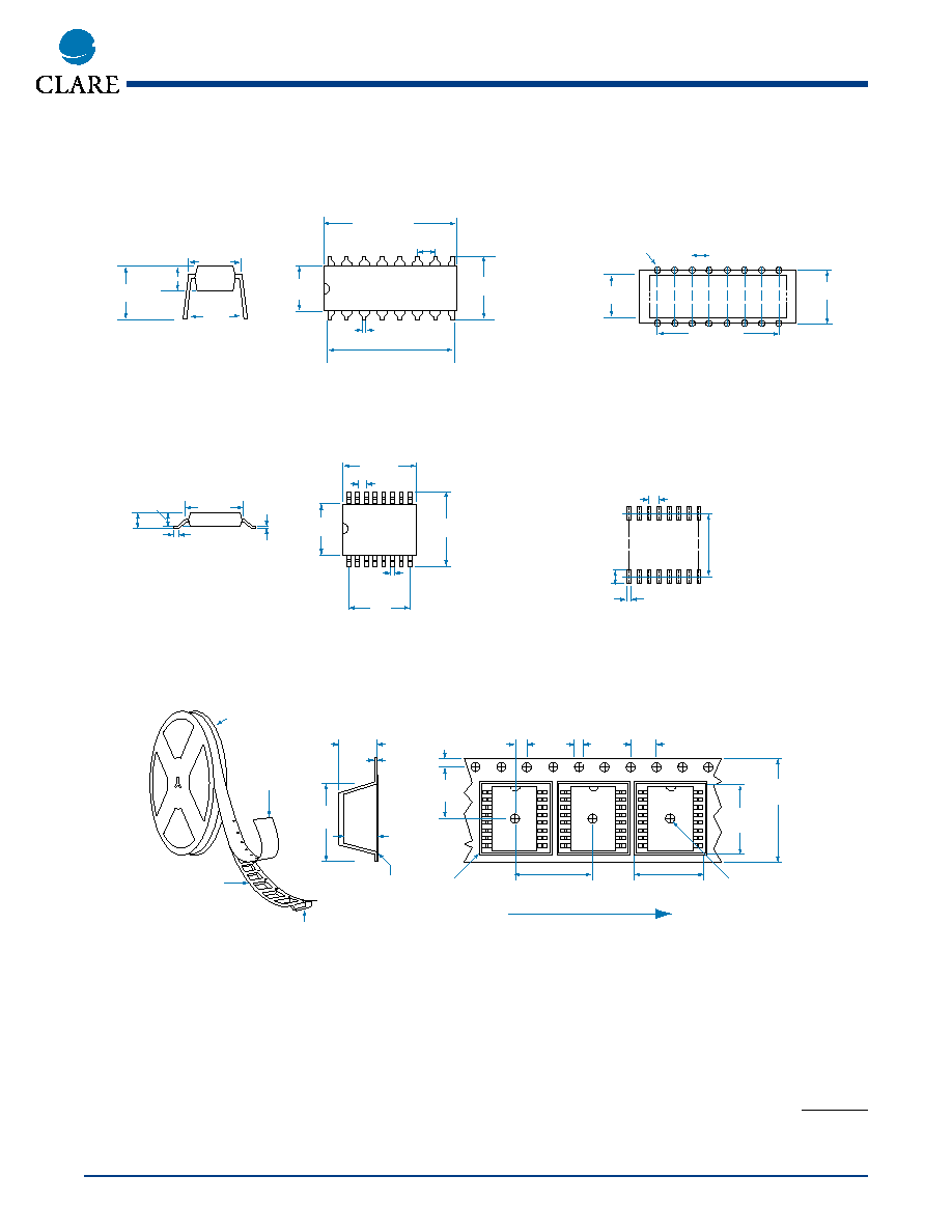
Dimensions
mm
(inches)
Mechanical Dimensions
7.493
±
.051
(.295
±
.002)
7.493
±
.127
(.295
±
.005)
.254
(.010)
1.270 TYP.
(.050)
2.108 MAX.
(.083)
1.981 TYP.
(.078)
1.016
(.040)
10.363
±
.127
(.408
±
.005)
8.890 TYP.
(.350)
.406 TYP.
(.016)
10.160
±
.051
(.400
±
.002)
16 Pin SOIC ("P" Suffix)
PC Board Pattern
(Top View)
1.193
(.047)
9.728
±
.051
(.383
±
.002)
.787
(.031)
1.270
(.050)
Tape and Reel Packaging for 16 Pin SOIC Package
7.493
±
.102
(.295
±
.004)
12.090
(.476)
1.753
±
.102
(.069
±
.004)
3.987
±
.102
(.157
±
.004)
1.498
±
.102
(.059
±
.004)
6.731 MAX.
(.265)
.406 MAX.
(.016)
3.175
(.125)
Top Cover
Tape
2.007
±
.102
(.079
±
.004)
11.989
±
.102
(.472
±
.004)
User Direction of Feed
.050R TYP.
16.002
±
.305
(.630
±
.012)
10.693
±
.025
(.421
±
.001)
Embossment
Embossed Carrier
Top Cover
Tape Thickness
.102 MAX.
(.004)
10.897
±
.025
(.429
±
.001)
1.549
±
.102
(.061
±
.004)
330.2 DIA.
(13.00)
1
16
6.350
±
.127
(.250
±
.005)
19.202
±
.381
(.756
±
.015)
2.540
±
.127
(.100
±
.005)
9.144 TYP.
(.360)
.457
±
.076
(.018
±
.003)
17.780
±
.127
(.700
±
.005)
16 Pin DIP Through Hole (Standard)
7.620 TYP.
(.300)
3.429 TYP.
(.135)
7.620
±
.254
(.300
±
.010)
9.144 TYP.
(.360)
PC Board Pattern
(Top View)
6.350
±
.127
(.250
±
.005)
2.540
±
.127
(.100
±
.005)
7.620
±
.127
(.300
±
.005)
17.780
±
.127
(.700
±
.005)
16-.800 DIA.
(16-.031 DIA.)