 | –≠–ª–µ–∫—Ç—Ä–æ–Ω–Ω—ã–π –∫–æ–º–ø–æ–Ω–µ–Ω—Ç: M-8888 | –°–∫–∞—á–∞—Ç—å:  PDF PDF  ZIP ZIP |

www.clare.com
DS-M8888-R1
M-8888
DTMF Transceiver
1
Features
∑
Advanced CMOS technology for low power con-
sumption and increased noise immunity
∑
Complete DTMF transmitter/receiver in a single
chip
∑
Standard 8051, 8086/8 microprocessor port
∑
Central office quality and performance
∑
Adjustable guard time
∑
Automatic tone burst mode
∑
Call progress mode
∑
Single +5 Volt power supply
∑
20-pin DIP and SOIC packages
∑
2 MHz microprocessor port operation
∑
Inexpensive 3.58 MHz crystal
Applications
∑
Paging systems
∑
Repeater systems/mobile radio
∑
Interconnect dialers
∑
PBX systems
∑
Computer systems
∑
Fax machines
∑
Pay telephone
∑
Credit card verification
Description
The M-8888 is a complete DTMF Transmitter
Receiver that features adjustable guard time, auto-
matic tone burst mode, call progress mode, and a fully
compatible 8051, 8086/8 microprocessor interface.
The receiver portion is based on the industry standard
M-8870 DTMF Receiver, while the transmitter uses a
switched-capacitor digital-to-analog converter for low-
distortion, highly accurate DTMF signaling. Tone
bursts can be transmitted with precise timing by mak-
ing use of the automatic tone burst mode. To analyze
call progress tones, a call progress filter can be select-
ed by an external microprocessor.
Ordering Information
Pin Connections
Block Diagram
Part #
Description
M-8888-01P
20-pin plastic DIP
M-8888-01SM
20-pin plastic SOIC
M-8888-01T
20-pin plastic SOIC,Tape and Reel

www.clare.com
2
M-8888
Rev. 1
ing the amplifier inputs at V
DD
/2. Provisions are made
for the connection of a feedback resistor to the op-amp
output (GS) for gain adjustment. In a single-ended
configuration, the input pins should be connected as
shown in the Single-Ended Input Configuration above.
Differential Input Configuration above shows the nec-
essary connections for a differential input configura-
tion.
Receiver Section
The low and high group tones are separated by apply-
ing the DTMF signal to the inputs of two sixth-order
Single-Ended Input Configuration
Differential Input Configuration
Functional Description
M-8888 functions consist of a high-performance
DTMF receiver with an internal gain setting amplifier
and a DTMF generator that contains a tone burst
counter for generating precise tone bursts and paus-
es. The call progress mode, when selected, allows the
detection of call progress tones. A standard 8051,
8086/8 series microprocessor interface allows access
to an internal status register, two control registers, and
two data registers.
Input Configuration
The input arrangement consists of a differential input
operational amplifier and bias sources (V
REF
) for bias-
Pin Functions
Name
Description
IN+
Noninverting op-amp input.
IN-
Inverting op-amp input.
GS
Gain select. Gives access to output of front end differential amplifier for connection of feedback resistor.
V
REF
Reference voltage output. Nominally V
DD
/2 is used to bias inputs at mid-rail.
V
SS
Negative power supply input.
OSC1
DTMF clock/oscillator input.
OSC2
Clock output. A 3.5795 MHz crystal connected between OSC1 and OSC2 completes the internal oscillator circuit.
TONE
Dual tone multifrequency (DTMF) output.
WR
Write input. A low on this pin when CS is low enables data transfer from the microprocessor. TTL compatible.
CS
Chip select. TTL input (CS = 0 to select the chip).
RS0
Register select input. See Internal Register Functions on page 7. TTL compatible.
RD
Read input. A low on this pin when CS is low enables data transfer to the microprocessor. TTL compatible..
IRQ /CP
Interrupt request to microprocessor (open-drain output). Also, when call progress (CP) mode has been selected and
interrupt enabled, the IRQ/CP pin will output a rectangular wave signal representative of the input signal applied at the
input op-amp. The input signal must be within the bandwidth limits of the call progress filter. See Timing Diagrams on
page 11.
D0-D3
Microprocessor data bus. TTL compatible.
ESt
Early steering output. Presents a logic high once the digital algorithm has detected a valid tone pair (signal condition).
Any momentary loss of signal condition will cause ESt to return to a logic low.
St/GT
Steering input/guard time output (bidirectional). A voltage greater than V
TSt
detected at St causes the device to register
the detected tone pair and update the output latch. A voltage less than V
TSt
frees the device to accept a new tone pair. The
GT output acts to reset the external steering time-constant; its state is a function of ESt and the voltage on St.
V
DD
Positive power supply input.
M-8888
www.clare.com
3
Rev. 1
switched capacitor bandpass filters with bandwidths
that correspond to the low and high group frequencies
listed in the Tone Encoding/Decoding below. The low
group filter incorporates notches at 350 and 440 Hz,
providing excellent dial tone rejection. Each filter out-
put is followed by a single-order switched capacitor fil-
ter that smoothes the signals prior to limiting. Limiting
is performed by high-gain comparators with hysteresis
to prevent detection of unwanted low-level signals.
The comparator outputs provide full-rail logic swings
at the incoming DTMF signal frequencies.
A decoder employs digital counting techniques to
determine the frequencies of the incoming tones, and
to verify that they correspond to standard DTMF fre-
quencies. A complex averaging algorithm protects
against tone simulation by extraneous signals (such
as voice), while tolerating small deviations in frequen-
cy. The algorithm provides an optimum combination of
immunity to talkoff with tolerance to interfering fre-
quencies (third tones) and noise. When the detector
recognizes the presence of two valid tones (referred to
as signal condition), the early steering (ESt) output
goes to an active state. Any subsequent loss of signal
condition will cause ESt to assume an inactive state.
Steering Circuit:
Before a decoded tone pair is registered, the receiver
checks for a valid signal duration (referred to as "char-
acter recognition condition"). This check is performed
by an external RC time constant driven by ESt. A logic
high on ESt causes V
C
(see the Basic Steering Circuit
above) to rise as the capacitor discharges. Provided
that the signal condition is maintained (ESt remains
high) for the validation period (t
GTP
), V
C
reaches the
threshold (V
TSt
) of the steering logic to register the
tone pair, latching its corresponding 4-bit code (see
the Tone Encoding/Decoding on left) into the receive
data register.
At this point the StGT output is activated and drives V
C
to V
DD
. StGT continues to drive high as long as ESt
remains high. Finally, after a short delay to allow the
output latch to settle, the delayed steering output flag
goes high, signaling that a received tone pair has
been registered. It is possible to monitor the status of
the delayed steering flag by checking the appropriate
bit in the status register. If interrupt mode has been
selected, the IRQ/CP pin will pull low when the
delayed steering flag is active.
The contents of the output latch are updated on an
active delayed steering transition. This data is pre-
sented to the 4-bit bidirectional data bus when the
receive data register is read. The steering circuit works
in reverse to validate the interdigit pause between sig-
nals. Thus, as well as rejecting signals too short to be
considered valid, the receiver will tolerate signal inter-
ruptions (dropout) too short to be considered a valid
pause. This capability, together with the ability to
select the steering time constants externally, allows
the designer to tailor performance to meet a wide vari-
ety of system requirements.
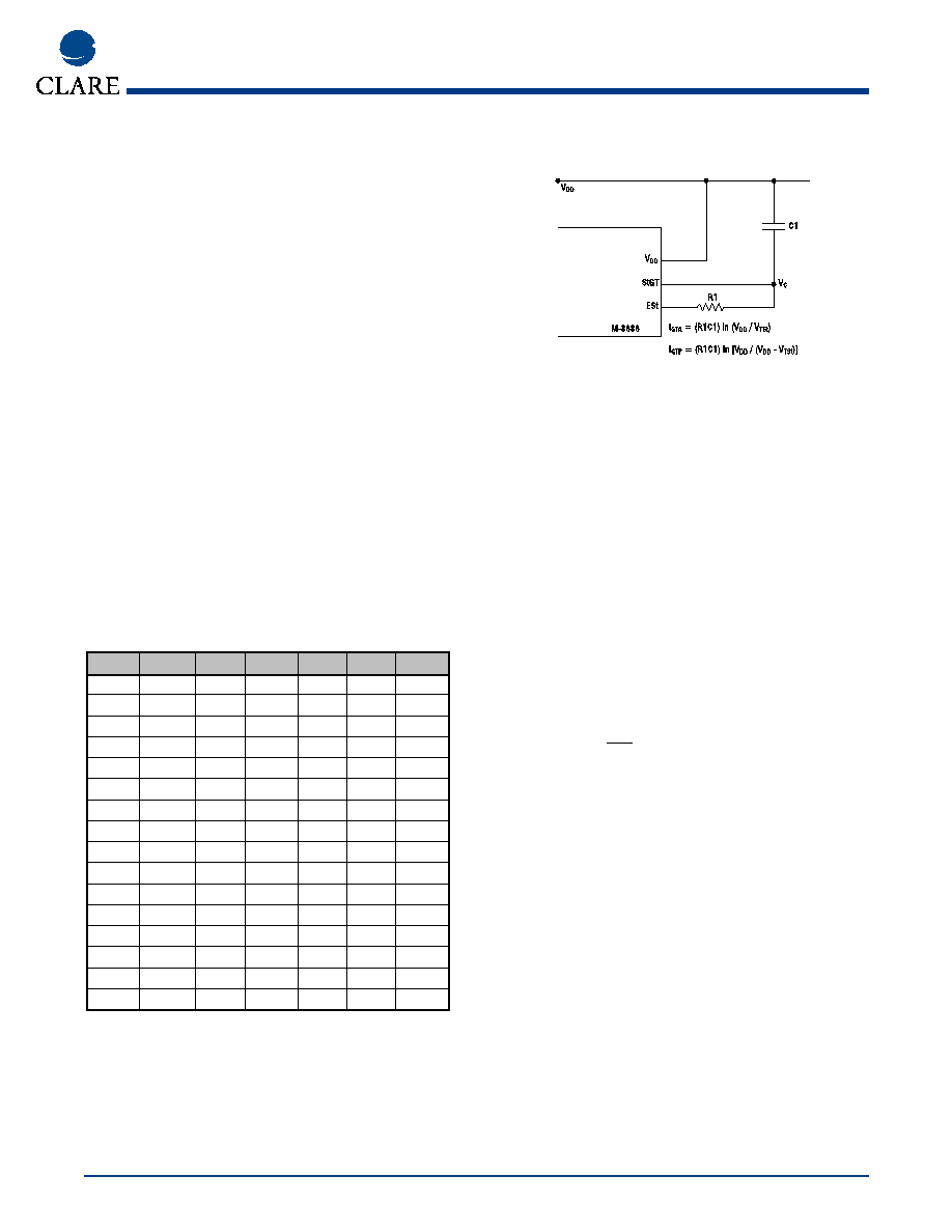
Guard Time Adjustment: The simple steering circuit
shown in the Basic Steering Circuit above is adequate
for most applications. Component values are chosen
according to the formula:
t
REC
= t
DP
+ t
GTP
T
ID
= t
DA
+ t
GTA
Tone Encoding/Decoding
F
LOW
F
HIGH
Digit
D3
D2
D1
D0
697
1209
1
0
0
0
1
697
1336
2
0
0
1
0
697
1477
3
0
0
1
1
770
1209
4
0
1
0
0
770
1336
5
0
1
0
1
770
1477
6
0
1
1
0
852
1209
7
0
1
1
1
852
1336
8
1
0
0
0
852
1477
9
1
0
0
1
941
1336
0
1
0
1
0
941
1209
*
1
0
1
1
941
1477
#
1
1
0
0
697
1633
A
1
1
0
1
770
1633
B
1
1
1
0
852
1633
C
1
1
1
1
941
1633
D
0
0
0
0
0 = logic low, 1 = logic high
Basic Steering Circuit

www.clare.com
4
M-8888
Rev. 1
The value of t
DP
is a device parameter and t
REC
is the
minimum signal duration to be recognized by the
receiver. A value for C1 of 0.1
µF is recommended for
most applications, leaving R1 to be selected by the
designer. Different steering arrangements may be
used to select independently the guard times for tone
present (t
GTP
) and tone absent (t
GTA
). This may be nec-
essary to meet system specifications that place both
accept and reject limits on both tone duration and inter-
digit pause. Guard time adjustment also allows the
designer to tailor system parameters such as talkoff
and noise immunity. Increasing t
REC
improves talkoff
performance since it reduces the probability that tones
simulated by speech will maintain signal condition long
enough to be registered. Alternatively, a relatively short
t
REC
with a long t
DO
would be appropriate for extreme-
ly noisy environments where fast acquisition time and
immunity to tone dropouts are required. Design infor-
mation for guard time adjustment is shown in the
Guard Time Adjustment above.
Call Progress Filter
A call progress (CP) mode can be selected, allowing
the detection of various tones that identify the progress
of a telephone call on the network. The call progress
tone input and DTMF input are common; however, call
progress tones can only be detected when the CP
mode has been selected. DTMF signals cannot be
detected if the CP mode has been selected (see the
Actual Frequencies vs Standard Requirements on
page 5). The Call Progress Response above indicates
the useful detect bandwidth of the call progress filter.
Frequencies presented to the input (IN+ and IN-) that
are within the accept bandwidth limits of the filter are
hard-limited by a high-gain comparator with the
IRQ/CP pin serving as the output. The square wave
output obtained from the schmitt trigger can be ana-
yzed by a microprocessor or counter arrangement to
determine the nature of the call progress tone being
detected. Frequencies in the reject area will not be
detected, and consequently there will be no activity on
IRQ/CP as a result of these frequencies.
DTMF Generator
The DTMF transmitter used in the M-8888 is capable
of generating all 16 standard DTMF tone pairs with low
distortion and high accuracy. All frequencies are
derived from an external 3.58 MHz crystal. The sinu-
soidal waveforms for the individual tones are digitally
synthesized using row and column programmable
dividers and switched capacitor digital-to-analog con-
verters. The row and column tones are mixed and fil-
tered, providing a DTMF signal with low total harmonic
distortion and high accuracy. To specify a DTMF sig-
nal, data conforming to the encoding format shown in
the Tone Encoding/Decoding Table on page 3 must be
written to the transmit data register. Note that this is the
same as the receiver output code. The individual tones
that are generated (f
LOW
and f
HIGH
) are referred to as
low-group and high-group tones. Typically, the high-
group to low-group amplitude ratio (twist) is 2 dB to
compensate for high-group attenuation on long loops.
Operation:
During write operations to the transmit data register, 4-
bit data on the bus is latched and converted to a 2 of 8
code for use by the programmable divider circuitry to
specify a time segment length that will ultimately deter-
mine the tone frequency. The number of time seg-
ments is fixed at 32, but the frequency is varied by
varying the segment length. When the divider reaches
the appropriate count as determined by the input code,
a reset pulse is issued and the counter starts again.
Guard Time Adjustment
Call Progress Response

Control Register A Description
Bit
Name
Function
Description
b0
TOUT
Tone output
A logic 1 enables the tone output. This function can be implemented in either the burst
mode or nonburst mode.
b1
CP/DTMF
Mode control
In DTMF mode (logic 0), the device is capable of generating and receiving DTMF signals.
When the call progress (CP) mode is selected (logic 1), a 6th-order bandpass filter is enabled to allow
call progress tones to be detected. Call progress tones within the specified bandwidth will be presented
at the IRQ/CP pin in rectangular wave format if the IRQ bit has been enabled (b2 = 1). Also, when the
CP mode and burst mode have both been selected, the transmitter will issue DTMF signals with a burst
and pause of 102 ms (typ) duration. This signal duration is twice that obtained from the DTMF transmit-
ter, if DTMF mode had been selected. Note that DTMF signals cannot be decoded when the CP mode
has been selected.
b2
IRQ
Interrupt enable
A logic 1 enables the interrupt mode. When this mode is active and the DTMF mode has
been selected (b1 = 0), the IRQ/CP pin will pull to a logic 0 condition when either (1) a valid DTMF sig-
nal has been received and has been present for the guard time or (2) the transmitter is ready for more
data (burst mode only).
b3
RSEL
Register select
A logic 1 selects control register B on the next write cycle to the control register address. Subsequent
write cycles to the control register are directed back to control register A.
Active Cell
Output Frequency(Hz)
% Error
Specified
Actual
L1
697
699.1
+ 0.30
L2
770
766.2
- 0.49
L3
852
847.4
- 0.54
L4
941
948.0
+ 0.74
H1
1209
1215.9
+ 0.57
H2
1336
1331.7
- 0.32
H3
1447
1471.9
- 0.35
H4
1633
1645.0
+ 0.73
M-8888
www.clare.com
5
Rev. 1
The divider output clocks another counter that
addresses the sinewave lookup ROM. The lookup
table contains codes used by the switched capacitor
D/A converter to obtain discrete and highly accurate
DC voltage levels. Two identical circuits are used to
produce row and column tones, which are then mixed
using a low-noise summing amplifier. The oscillator
described needs no startup time as in other DTMF
generators, since the crystal oscillator is running con-
tinuously, thus providing a high degree of tone burst
accuracy. When there is no tone output signal, the
TONE pin assumes a DC level of 2.5 volts (typically).
A bandwidth limiting filter is incorporated to attenuate
distortion products above 4 KHz.
Burst Mode:
Certain telephony applications require that generated
DTMF signals be of a specific duration, determined
either by the application or by any of the existing
exchange transmitter specifications. Standard DTMF
signal timing can be accomplished by making use of
the burst mode. The transmitter is capable of issuing
symmetric bursts/pauses of predetermined duration.
This burst/pause duration is 51 ms ± 1 ms, a standard
interval for autodialer and central office applications.
After the burst/pause has been issued, the appropriate
bit is set in the status register, indicating that the trans-
mitter is ready for more data.
The timing described in the previous paragraph is
available when the DTMF mode has been selected.
However, when call progress (CP) mode is selected, a
secondary burst/pause time is available that extends
this interval to 102 ms ± 2 ms. The extended interval is
useful when precise tone bursts of longer than 51 ms
duration and 51 ms pause are desired. Note that when
CP mode and burst mode have been selected, DTMF
tones may be transmitted only and not received. In
applications where a nonstandard burst/pause time is
desirable, a software timing loop or external timer can
be used to provide the timing pulses when the burst
mode is disabled by enabling and disabling the trans-
mitter.
The M-8888 is initialized on powerup sequence with
DTMF mode and burst mode selected.
Single-Tone Generation:
A single-tone mode is available whereby individual
tones from the low group or high group can be gener-
ated. This mode can be used for DTMF test equipment
applications, acknowledgment tone generation, and
distortion measurements. Refer to the Control Register
B Description below for details.
Actual Frequencies vs Standard Requirements