Voltage: 250 Volts
Current: 0.2Amp
BAS21
Feature
High Voltage Switching Diode
Surface Mount Package Ideally Suited for
Automatic Insertion
For General Purpose Switching
Applications
Surface Mount Switching Diode
www.comchip.com.tw
COMCHIP
COMCHIP
Rating
Symbol
Value
Units
Continuous Reverse Voltage
V
R
250
V
DC
Peak Forward Current
I
F
200.0
mAdc
Peak Surge Forward Current
I
FSM
(surge)
625
mAdc
Characteristic
Symbol
Max
Units
Total Device Dissipation FR≠ 5 Board(1) T
A
= 25∞C
225.0
mW
Derate above 25∞C
1.8
mW/∞C
Thermal Resistance, Junction to Am bient
R
JA
556.0
∞C/W
Total Device Dissipation Alumina Substrate,(2) T
A
= 25∞C
300
mW
Derate above 25∞C
2.4
mW/∞C
Thermal Resistance, Junction to Am bient
R
JA
417
∞C/W
Junction and Storage Temperature
T
J
, T
stg
≠55 to +150
∞C
Characteristic
Symbol
Min
Max
Units
Reverse Voltage Leakage Current V
R
= 200 Vdc
-
1.0
V
R
= 200 Vdc, TJ = 150∞C
-
100
Reverse Breakdown Voltage (BR = 100 Adc)
V(BR)
250
-
Vdc
Forward Voltage F = 100 mAdc
1000
F = 200 mAdc
1250
Diode Capacitance (V
R
= 0, f = 1.0 MHz))
C
D
5
pF
Reverse Recovery Time (I
F
= IR = 30 mAdc, RL = 100 )
Trr
50
nS
mV
1.FR≠5 = 1.0 X 0.75X 0.062 in. 2.Alumina = 0.4X 0.3X 0.024 in. 99.5% alumina.
P
D
Electrical Characterics
(TA = 25∞C unless otherwise noted)
I
R
VF
Maximum Ratings
Thermal Characteristics
P
D
uAdc
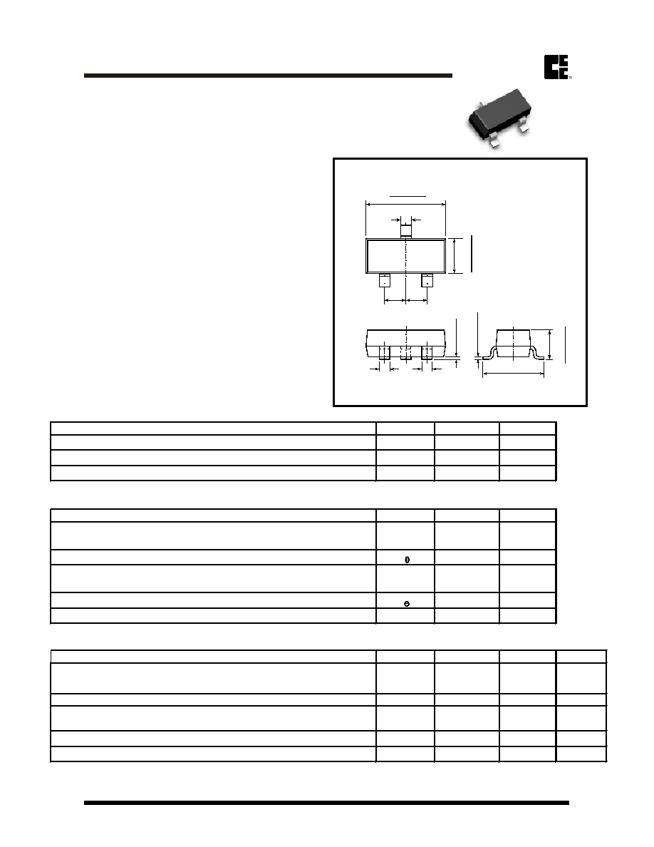
SOT-23
Dimensions in inches (millimeters)
Mechanical Data
Case: SOT -23, Plastic
Terminals : Solderable per NIL-STD -202,
Method 208
Approx. Weight: 0.008 gram
MDS0209006A
Page 1
.037(0.95) .037(0.95)
.00
6
(0
.
1
5
)
max.
.1
19
(3.
0
)
.0
20
(0.
5
)
.0
20
(0.
5
)
Top View
.10
3
(2.6)
.00
6
(
0
.15)
.0
4
4
(1
.
1
0
)
.110 (2.8)
.0
47
(1
.
2
0
)
.00
2
(0
.
0
5)
.0
86
(2.
2
)
.0
3
5
(0
.
9
0
)
.0
20
(0.
5
)
.056 (
1
.4
0)
RATING AND CHARACTERISTIC CURVES (BAS21)
Surface Mount Switching Diode
Surface Mount Switching Diode
www.comchip.com.tw
COMCHIP
COMCHIP
MDS0209006A
Page 2
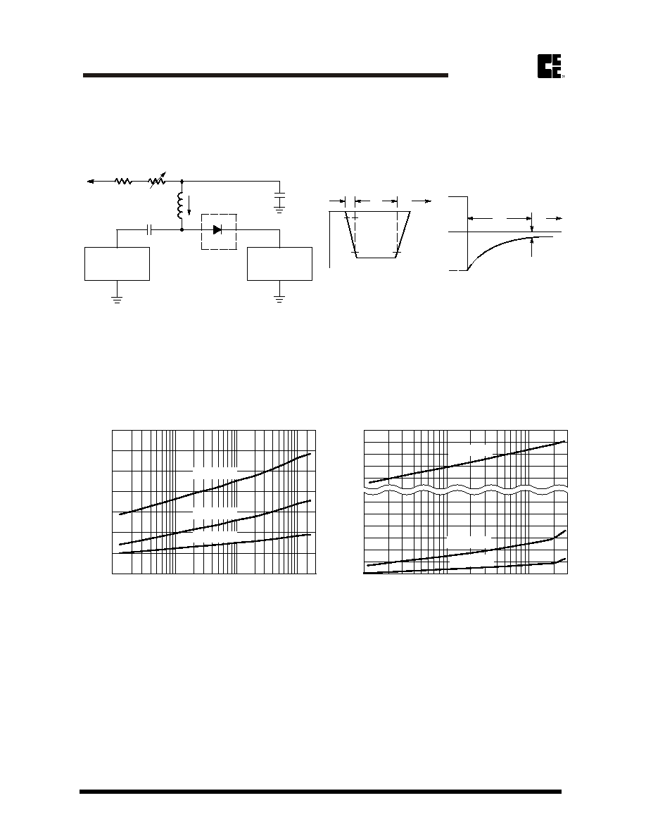
Notes: 1. A 2.0 k
variable resistor adjusted for a Forward Current (IF) of 10 mA.
Notes:
2. Input pulse is adjusted so IR(peak) is equal to 10 mA.
Notes:
3. tp ª trr
+10 V
2 k
820
0.1
µ
F
DUT
VR
100
µ
H
0.1
µ
F
50
utput
P
ulse
Generator
50
Input
S
ampling
Oscilloscope
tr
tp
t
10%
90%
IF
IR
trr
t
I
R(REC) = 1 mA
Output Pulse
(IF = IR = 10 mA; measured
at
I
R(REC) = 1 mA)
IF
Input Signal
Figure 1. Recovery Time Equivalent Test Circuit
Figure 2. Forward Voltage
Figure 3. Reverse Leakage
3500
F
orward
V
oltage (mV)
Forward Current (mA)
2500
1500
500
0
0.2
0.5
2
1
3000
2000
1000
5
10
20
50
100
200
0.1
7000
Reverse
Current
(nA)
Reverse Voltage (V)
5000
3000
5
0
2
1
6000
4000
6
5
10
20
50
100
200
1
2
3
4
TA = 155
∞
C
TA = ≠55
∞
C
TA = 25
∞
C
300
TA = 155
∞
C
TA = 25
∞
C
TA = ≠55
∞
C