Reverse Voltage: 20 - 100 Volts
Forward Current: 1.0 Amp
CDBA120 Thru CDBA1100
GS
Features
Ideal for surface mount applications
Easy pick and place
Plastic package has Underwriters Lab.
flammability classification 94V-0
Built-in strain relief
Low forward voltage drop
Mechanical data
Case: JEDEC DO-214AC molded plastic
Terminals: solderable per MIL-STD-750,
method 2026
Polarity: Color band denotes cathode
end
Mounting position: Any
Approx. weight:0.064 gram
SMD Schottky Barrier Rectifier
SMD Schottky Barrier Rectifier
www.comchip.com.tw
COMCHIP
COMCHIP
Parameter
Max. Repetitive Peak Reverse Voltage
Max. DC Blocking Voltage
Max. RMS Voltage
Peak Surge Forward Current
8.3ms single half sine-wave
superimposed on rate load
( JEDEC method )
Max. Average Forward Current
Max. Instantaneous Forward Current
at 1.0 A
Max. DC Reverse Current at Rated DC
Blocking Voltage Ta=25
Ta=100
Max. Thermal Resistance (Note 1)
Operating Junction Temperature
Storage Temperature
Symbol
V
RRM
V
DC
V
RMS
I
FSM
I o
V
F
I
R
R
JA
R
JL
T j
T
STG
Maximum Ratings and Electrical Characterics
Unit
V
V
V
A
A
V
.
mA
C/W
MDS0208007C
Page 1
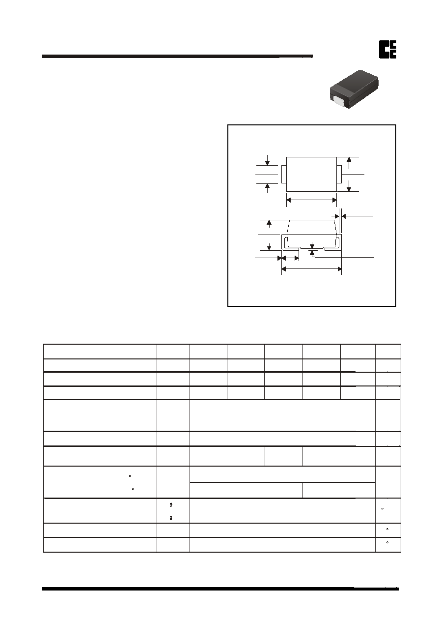
Dimensions in inches and (millimeters)
0.008(0.20)
0.004(0.10)
0.067(1.70)
0.051(1.29)
0.090(2.29)
0.067(1.70)
0.059(1.50)
0.035(0.89)
0.110(2.79)
0.086(2.18)
0.180(4.57)
0.160(4.06)
0.012(0.31)
0.006(0.15)
0.209(5.31)
0.185(4.70)
DO-214AC (SMA)
Note 1: Thermal resistance from junction to ambient and junction to to lead P.C.B. Mounted on 0.2 x 0.2 copper pad areas
CDBA120
GS CDBA1100GS
CDBA180
GS
CDBA160
GS
CDBA140
GS
20
20
14
100
100
70
80
80
56
60
60
42
40
40
28
35
1.0
0.50
0.85
0.70
- 5 0 t o + 1 2 5
88
20
0.5
- 6 5 t o + 1 5 0
5
10
C
C
C
C

50
Rating and Characteristic Curves (CDBA120
GS Thru CDBA1100GS)
Fig. 1 - Reverse Characteristics
Percent of Rated Peak Reverse Voltage (%)
R
e
v
e
r
s
e
C
u
r
r
e
n
t
(
m
A
)
Fig. 4 - Current Derating Curve
0
0.6
1.2
160
20
40
60
80
100
120 140
A
v
e
r
a
g
e
F
o
r
w
a
r
d
C
u
r
r
e
n
t
(
A
)
www.comchip.com.tw
COMCHIP
COMCHIP
0 20 40 60 80 100 120 140 160 180 200
F
o
r
w
a
r
d
C
u
r
r
e
n
t
(
A
)
Forward Voltage (V)
Fig.2 - Forward Characteristics
0.01 0.1 1.0 10 100
50
MDS0208007C
Page 2
Fig. 3 - Junction Capacitance
Reverse Voltage (V)
0.1 0.3 0.5 0.7 0.9 1.1 1.3 1.5 1.7 1.9 2.1
J
u
n
c
t
i
o
n
C
a
p
a
c
i
t
a
n
c
e
(
p
F
)
0
100
150
350
SMD Schottky Barrier Rectifier
SMD Schottky Barrier Rectifier
0.2
0.4
1.0
0.8
300
250
200
P
e
a
k
s
u
r
g
e
F
o
r
w
a
r
d
C
u
r
r
e
n
t
(
A
)
Fig. 5 - Non repetitive forward
surge current
0
10
20
40
30
1 5 10 50 1 00
Number of Cycles at 60Hz
1
100
10
0.1
0.01
1
100
10
0.1
0.01
Tj=75 C
Tj=25 C
Tj=25 C
Pulse width 300uS
4% duty cycle
C
D
B
A
1
2
0-
140
GS
C
D
B
A
1
6
0
-1
1
0
0GS
Tj=25 C
Ambient Temperature ( C)
8.3mS Single Half Sine
Wave JEDEC methode
CDBA180-1100
GS
CDBA160
GS
=1MHz and applied
4VDC reverse voltage
CDBA120-140
GS