
Io = 30mA
V
R
= 40 Volt s
CDBN00340
Features
Designed for mounting on small surface
Extremely thin package
Low stored charge
Majority carrier conduction
Mechanical data
Case: 12063(3216)Standard package,
molded plastic.
Terminals: Solder plated, solderable per
MIL-STD-750, method 2026.
Polarity: Indicated by cathode band.
Mounting position: Any.
Weight: 0.0085 gram. (approximately)
SMD Schottky Barrier Diode
SMD Schottky Barrier Diode
Unit
V
uA
uA
pF
Parameter
Forward voltage
Reverse current
Reverse current
Capacitance between terminals
Conditions
I
F
= 1 mA DC
V
R
= 40 V
V
R
= 30 V
f = 1MHz, and 1 VDC reverse voltage
Symbol
V
F
I
R
I
R
C
T
Min
Typ
2
Max
0.37
1.00
0.50
www.comchip.com.tw
COMCHIP
COMCHIP
Page 1
Parameter
Repetitive peak reverse voltage
Reverse voltage
Average forward current
Forward current, surge peak
Power Dissipation
Storage temperature
Junction temperature
Conditions
8.3 ms single half sine-wave superimposed
on rate load ( JEDEC method )
Symbol
V
RRM
V
R
Io
I
FSM
P
D
T
STG
T j
Min
-40
-40
Max
45
40
30
200
+125
+125
Typ
500
Unit
V
V
mA
mA
mW
0.126(3.20)
0.118(3.00)
0.020(0.50) Typ.
0.063(1.60)
0.055(1.40)
0.043 (1.10)
0.035(0.90)
0.010(R0.25) Typ.
Dimensions in inches and (millimeter)
1206 (3216)
Maximum Rating
( at T
A
= 25 unless otherwise noted )
C
C
C
C
Electrical Characteristics
( at T
A
= 25 unless otherwise noted )
C
C
RDS0208006-C
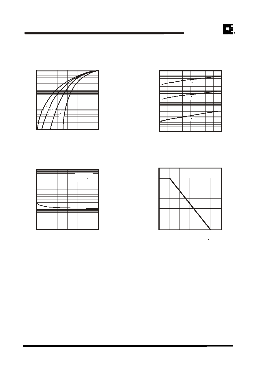
RATING AND CHARACTERISTIC CURVES (CDBN00340)
F
o
r
w
a
r
d
c
u
r
r
e
n
t
(
A
)
Fig. 1 - Forward characteristics
Forward voltage (V)
Reverse voltage (V)
Fig. 1 - Forward characteristics
R
e
v
e
r
s
e
c
u
r
r
e
n
t
(
A
)
Fig. 4 - Derating curve
0
20
40
60
80
100
0
25
50
75
100
125
150
Mounting on glass epoxy PCBs
A
v
e
r
a
g
e
f
o
r
w
a
r
d
c
u
r
r
e
n
t
(
%
)
www.comchip.com.tw
COMCHIP
COMCHIP
Fig. 3 - Capacitance between
terminals characteristics
Reverse voltage (V)
C
a
p
a
c
i
t
a
n
c
e
b
e
t
w
e
e
n
t
e
r
m
i
n
a
l
s
(
p
F
)
0.1
1
10
20
SMD Schottky Barrier Diode
SMD Schottky Barrier Diode
Page 2
30
0
5
10
15
20
25
10u
100u
1m
10m
0.1
0.2
0.4
0.6
0
0.5
0.3
100u
10u
10n
100n
1u
10
20
30
40
0
C
1
2
5
C
7
5
C
2
5
C
-2
5
C
125
C
75
C
25
Ambient temperature ( )
C
C
f = 1 MHz
Ta = 25 C
RDS0208006-C