Reverse Voltage: 50 - 600 Volts
Forward Current: 1.0 Amp
CEFL101 Thru CEFL105
Maximum Ratings and Electrical Characterics
MDS0210022B
Page 1
SMD Efficient Fast Recovery Rectifier
SMD Efficient Fast Recovery Rectifier
Parameter
Max. Repetitive Peak Reverse Voltage
Max. DC Blocking Voltage
Max. RMS Voltage
Peak Surge Forward Current
8.3ms single half sine-wave
superimposed on rate load
( JEDEC method )
Max. Average Forward Current
Max. Instantaneous Forward Current
at 2.0 A
Reverse recovery time
Max. DC Reverse Current at Rated DC
Blocking Voltage Ta=25
Ta=100
Typical. Thermal Resistance (Note 1)
Operating Junction Temperature
Storage Temperature
Symbol
V
RRM
V
DC
V
RMS
I
FSM
I o
V
F
Trr
I
R
R
JL
T j
T
STG
Unit
V
V
V
A
A
V
nS
uA
Note 1: Thermal resistance from junction to lead P.C.B. Mounted on 8.0x8.0 mm copper pad areas.
CEFL CEFL CEFL CEFL CEFL
101 102 103 104 105
50
50
35
600
600
420
100
100
70
1.0
- 5 5 t o + 1 5 0
50
5.0
250
- 5 5 t o + 1 5 0
400
400
280
200
200
140
C/W
C
C
C
C
Features
Ideal for surface mount applications
Easy pick and place
Plastic package has Underwriters Lab.
flammability classification 94V-0
Super fast recovery time for high efficient
Built-in strain relief
Low forward voltage drop
Mechanical Data
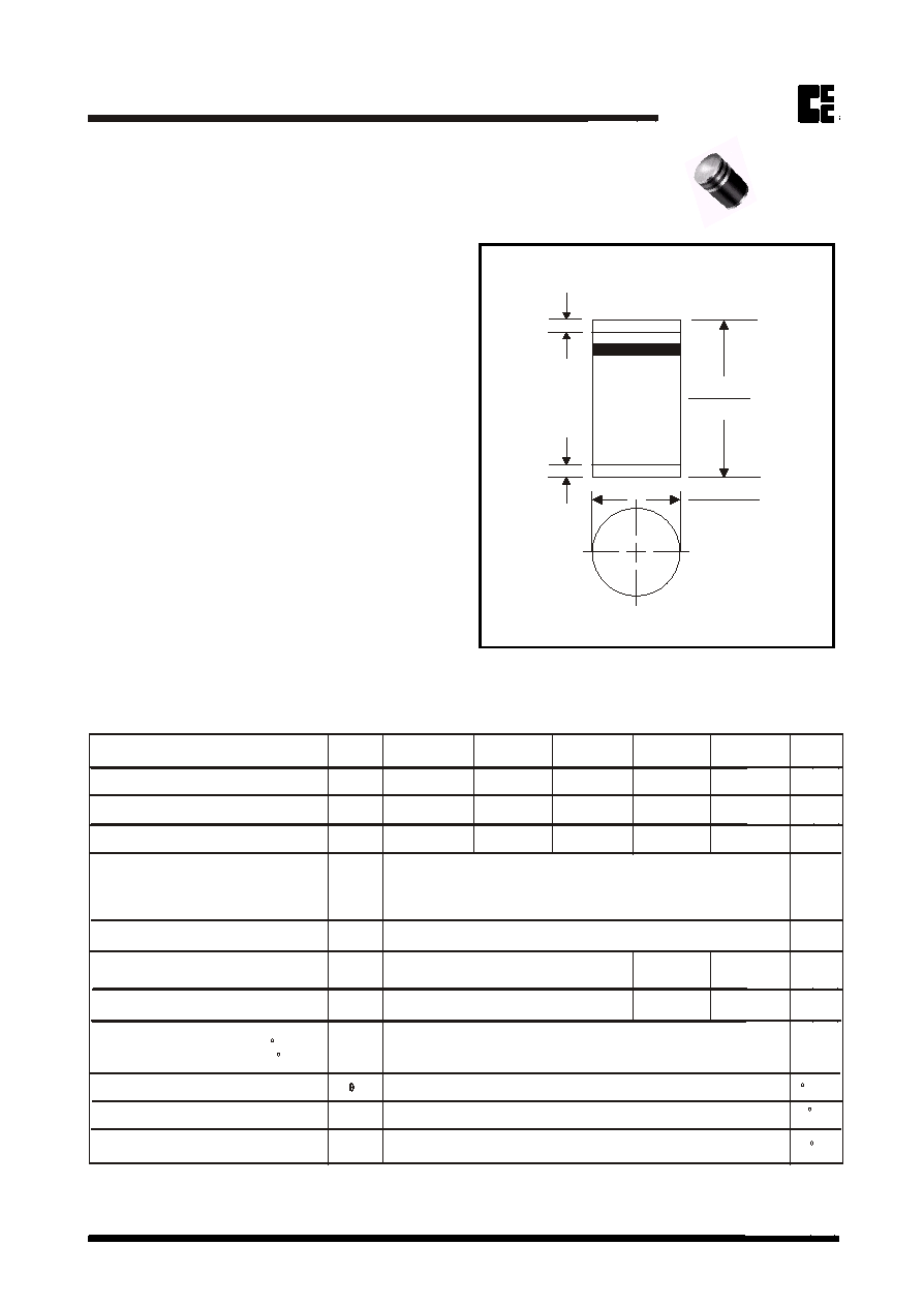
Case: Mini-SMA/SOD-123 molded plastic
Terminals: solderable per MIL-STD-750,
method 2026
Polarity: Color band denotes cathode
end
Mounting position: Any
Approx. Weight:0.116 gram
30
0.875 1.1 1.25
25 35 50
Dimensions in inches and (millimeters)
0.205(5.2)
0.195(4.8)
0.022(0.55)
Max.
0.105(2.67)
0.095(2.40)
DO-213AB (Plastic Melf)
www.comchiptech.com
COMCHIP
COMCHIP
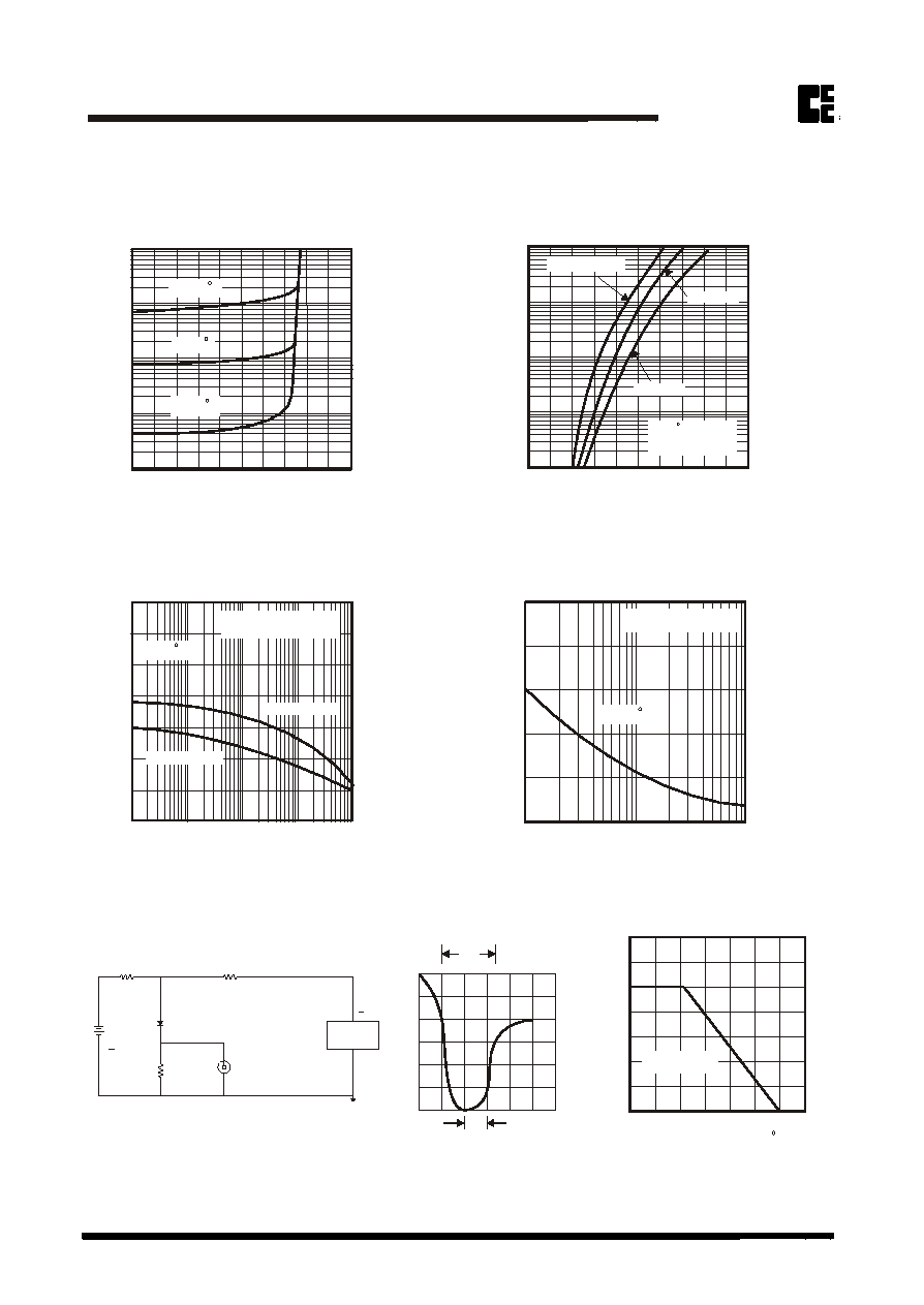
Rating and Characteristic Curves (CEFL101 Thru CEFL105)
F
o
r
w
a
r
d
c
u
r
r
e
n
t
(
A
)
Forward Voltage (V)
Fig.2 - Forward Characteristics
MDS0210022B
Page 2
0 0.2 0.4 0.6 0.8 1.0 1.2 1.4 1.6 1.8 2.0
P
e
a
k
S
u
r
g
e
F
o
r
w
a
r
d
C
u
r
r
e
n
t
(
A
)
Fig. 4 - Non Repetitive Forward
Surge Current
Number of Cycles at 60Hz
SMD Efficient Fast Recovery Rectifier
SMD Efficient Fast Recovery Rectifier
Fig. 6 - Current Derating Curve
Fig. 5 - Test Circuit Diagram and Reverse Recovery Time Characteristics
(+)
(+)
25Vdc
(approx.)
( )
( )
PULSE
GENERATOR
(NOTE 2)
OSCILLISCOPE
(NOTE 1)
1
NON-
INDUCTIVE
W
NOTES: 1. Rise Time= 7ns max., Input Impedance= 1 megohm.22pF.
2. Rise Time= 10ns max., Source Impedance= 50 ohms.
+0.5A
0
-0.25A
-1.0A
|
|
|
|
|
|
|
|
1cm
SET TIME BASE FOR
50 / 10ns / cm
trr
D.U.T.
10
NONINDUCTIVE
50
NONINDUCTIVE
W
W
0
10
20
50
40
30
1 5 10 50 1 00
10
1.0
0.1
0.01
0.001
Single Phase
Half Wave 60Hz
0 15 30 45 60 75 90 105 120 135 150
100
10
1.0
0.1
0. 01
Percent of Rated Peak Reverse Voltage (%)
R
e
v
e
r
s
e
C
u
r
r
e
n
t
(
u
A
)
Fig. 1 - Reverse Characteristics
Tj=25 C
Tj=125 C
Tj=25 C
Pulse width 300uS
4% duty cycle
Tj=25 C
A
v
e
r
a
g
e
F
o
r
w
a
r
d
C
u
r
r
e
n
t
(
A
)
Ambient Temperature ( C)
0 25 50 75 100 125 150 175
2.8
2.4
2.0
1.6
1.2
0.8
0.4
0
8.3mS Single Half Sine
Wave JEDEC methode
Tj=75 C
0.01 0.1 1.0 10 100
Fig. 3 - Junction Capacitance
Reverse Voltage (V)
J
u
n
c
t
i
o
n
C
a
p
a
c
i
t
a
n
c
e
(
p
F
)
CEFL101-103
CEFL105
CEFL104
35
30
25
20
15
10
5
0
f=1MHz and applied
4VDC reverse voltage
Tj=25 C
CEFL101-103
CEFL104-105
www.comchiptech.com
COMCHIP
COMCHIP